Embed Size (px)
Citation preview
TC1054/TC1055/TC118650 mA, 100 mA and 150 mA CMOS LDOs with Shutdown and ERROR Output
Features
• Low Ground Current for Longer Battery Life
• Low Dropout Voltage
• Choice of 50 mA (TC1054), 100 mA (TC1055) and 150 mA (TC1186) Output
• High Output Voltage Accuracy
• Standard or Custom Output Voltages:
- 1.8V, 2.5V, 2.6V, 2.7V, 2.8V, 2.85V, 3.0V, 3.3V, 3.6V, 4.0V, 5.0V
• Power-Saving Shutdown Mode
• ERROR Output Can Be Used as a Low-Battery Detector or Microcontroller-Reset Generator
• Overcurrent and Overtemperature Protection
• 5-Pin SOT-23 Package
• Pin-Compatible Upgrades for Bipolar Regulators
Applications
• Battery Operated Systems
• Portable Computers
• Medical Instruments
• Instrumentation
• Cellular/GSM/PHS Phones
• Linear Post-Regulators for SMPS
• Pagers
Typical Application
General Description
The TC1054, TC1055 and TC1186 are high accuracy(typically ±0.5%) CMOS upgrades for older (bipolar)low dropout regulators. Designed specifically forbattery-operated systems, the devices’ CMOSconstruction minimizes ground current, extendingbattery life. Total supply current is typically 50 µA at fullload (20 to 60 times lower than in bipolar regulators).
The devices’ key features include low noise operation,low dropout voltage – typically 85 mV (TC1054),180 mV (TC1055) and 270 mV (TC1186) at full load —and fast response to step changes in load. An erroroutput (ERROR) is asserted when the devices areout-of-regulation (due to a low input voltage orexcessive output current). ERROR can be used as alow battery warning or as a processor RESET signal(with the addition of an external RC network). Supplycurrent is reduced to 0.5 µA (maximum), with bothVOUT and ERROR disabled when the shutdown input islow. The devices incorporate both overtemperatureand over-current protection.
The TC1054, TC1055 and TC1186 are stable with anoutput capacitor of only 1 µF, and have a maximumoutput current of 50 mA, 100 mA and 150 mA,respectively. For higher output current regulators,please refer to the TC1173 (IOUT = 300 mA) data sheet(DS21632).
Package Type
VOUT
GND
1 µF+
VIN VIN VOUT1 5
2
43SHDN
Shutdown Control(from Power Control Logic)
ERRORERROR
1 M
TC1054TC1055TC1186
Note: 5-Pin SOT-23 is equivalent to the EIAJ (SC-74A)
5
1
4
2 3
5-Pin SOT-23
TC1054TC1055TC1186
VOUT ERROR
SHDNGNDVIN
2002-2012 Microchip Technology Inc. DS21350E-page 1
TC1054/TC1055/TC1186
1.0 ELECTRICAL CHARACTERISTICS
Absolute Maximum Ratings †
Input Voltage ..................................................................6.75VOutput Voltage ..................................... (-0.3V) to (VIN + 0.3V)Power Dissipation ......................... Internally Limited (Note 6)Maximum Voltage on Any Pin ...................VIN +0.3V to -0.3VOperating Junction Temperature Range ..-40°C <TJ< +125°CStorage Temperature.....................................-65°C to +150°C
† Notice: Stresses above those listed under "AbsoluteMaximum Ratings" may cause permanent damage tothe device. These are stress ratings only and functionaloperation of the device at these or any other conditionsabove those indicated in the operation sections of thespecifications is not implied. Exposure to AbsoluteMaximum Rating conditions for extended periods mayaffect device reliability.
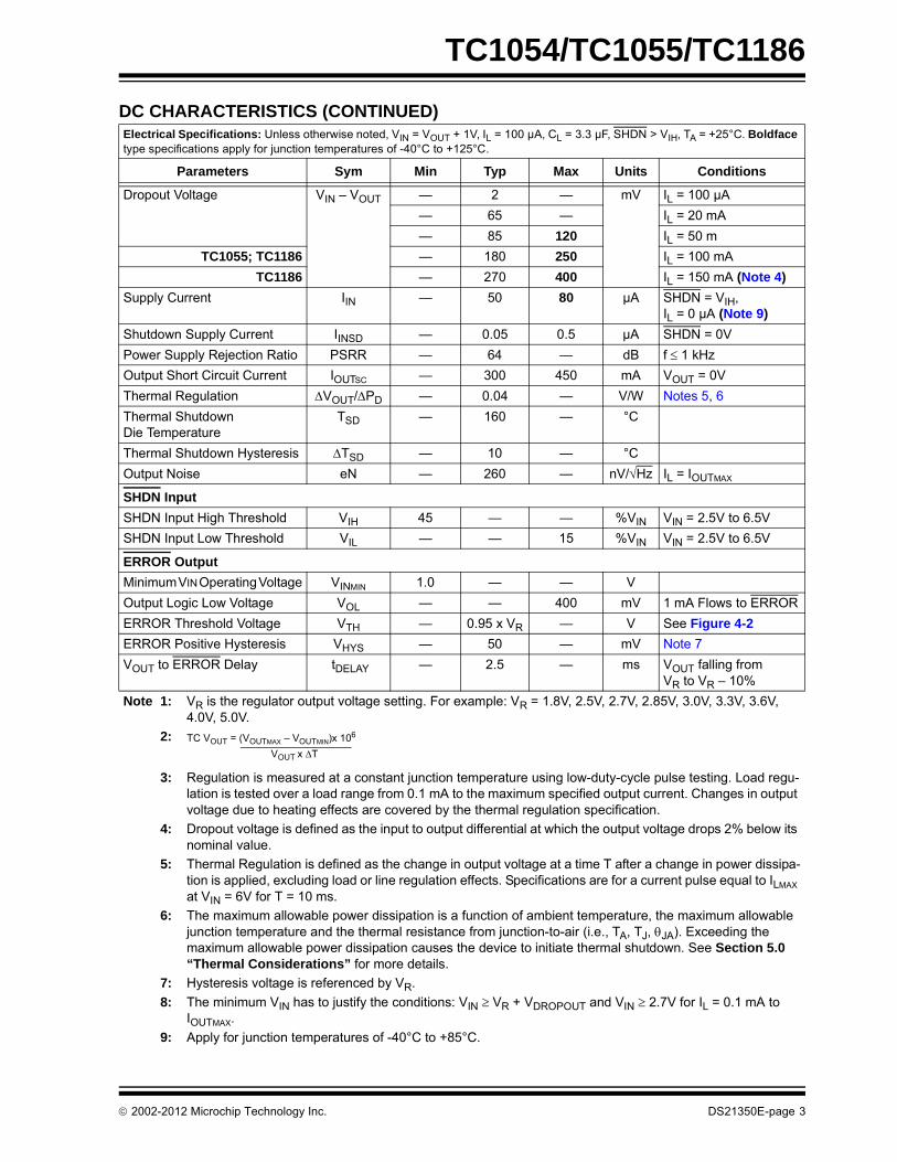
DC CHARACTERISTICSElectrical Specifications: Unless otherwise noted, VIN = VOUT + 1V, IL = 100 µA, CL = 3.3 µF, SHDN > VIH, TA = +25°C. Boldface type specifications apply for junction temperatures of -40°C to +125°C.
Parameters Sym Min Typ Max Units Conditions
Input Operating Voltage VIN 2.7 — 6.50 V Note 8
Maximum Output Current IOUTMAX 50 — — mA TC1054
100 — — TC1055
150 — — TC1186
Output Voltage VOUT VR – 2.5% VR ±0.5% VR + 2.5% V Note 1
VOUT Temperature Coefficient
TCVOUT — 20 — ppm/°C Note 2
— 40 —
Line Regulation VOUT/VIN — 0.05 0.35 % (VR + 1V) VIN6V
Load Regulation
TC1054; TC1055 VOUT/VOUT — 0.5 2 % (Note 3)IL = 0.1 mA to IOUTMAXTC1186 — 0.5 3
Note 1: VR is the regulator output voltage setting. For example: VR = 1.8V, 2.5V, 2.7V, 2.85V, 3.0V, 3.3V, 3.6V, 4.0V, 5.0V.
2:
3: Regulation is measured at a constant junction temperature using low-duty-cycle pulse testing. Load regu-lation is tested over a load range from 0.1 mA to the maximum specified output current. Changes in output voltage due to heating effects are covered by the thermal regulation specification.
4: Dropout voltage is defined as the input to output differential at which the output voltage drops 2% below its nominal value.
5: Thermal Regulation is defined as the change in output voltage at a time T after a change in power dissipa-tion is applied, excluding load or line regulation effects. Specifications are for a current pulse equal to ILMAX at VIN = 6V for T = 10 ms.
6: The maximum allowable power dissipation is a function of ambient temperature, the maximum allowable junction temperature and the thermal resistance from junction-to-air (i.e., TA, TJ, JA). Exceeding the maximum allowable power dissipation causes the device to initiate thermal shutdown. See Section 5.0 “Thermal Considerations” for more details.
7: Hysteresis voltage is referenced by VR.
8: The minimum VIN has to justify the conditions: VIN VR + VDROPOUT and VIN 2.7V for IL = 0.1 mA to IOUTMAX.
9: Apply for junction temperatures of -40°C to +85°C.
TC VOUT = (VOUTMAX – VOUTMIN)x 106
VOUT x T
DS21350E-page 2 2002-2012 Microchip Technology Inc.
TC1054/TC1055/TC1186
Dropout Voltage VIN – VOUT — 2 — mV IL = 100 µA
— 65 — IL = 20 mA
— 85 120 IL = 50 m
TC1055; TC1186 — 180 250 IL = 100 mA
TC1186 — 270 400 IL = 150 mA (Note 4)
Supply Current IIN — 50 80 µA SHDN = VIH, IL = 0 µA (Note 9)
Shutdown Supply Current IINSD — 0.05 0.5 µA SHDN = 0V
Power Supply Rejection Ratio PSRR — 64 — dB f 1 kHz
Output Short Circuit Current IOUTSC — 300 450 mA VOUT = 0V
Thermal Regulation VOUT/PD — 0.04 — V/W Notes 5, 6
Thermal Shutdown Die Temperature
TSD — 160 — °C
Thermal Shutdown Hysteresis TSD — 10 — °C
Output Noise eN — 260 — nV/Hz IL = IOUTMAX
SHDN Input
SHDN Input High Threshold VIH 45 — — %VIN VIN = 2.5V to 6.5V
SHDN Input Low Threshold VIL — — 15 %VIN VIN = 2.5V to 6.5V
ERROR Output
Minimum VIN Operating Voltage VINMIN 1.0 — — V
Output Logic Low Voltage VOL — — 400 mV 1 mA Flows to ERROR
ERROR Threshold Voltage VTH — 0.95 x VR — V See Figure 4-2
ERROR Positive Hysteresis VHYS — 50 — mV Note 7
VOUT to ERROR Delay tDELAY — 2.5 — ms VOUT falling from VR to VR – 10%
DC CHARACTERISTICS (CONTINUED)Electrical Specifications: Unless otherwise noted, VIN = VOUT + 1V, IL = 100 µA, CL = 3.3 µF, SHDN > VIH, TA = +25°C. Boldface type specifications apply for junction temperatures of -40°C to +125°C.
Parameters Sym Min Typ Max Units Conditions
Note 1: VR is the regulator output voltage setting. For example: VR = 1.8V, 2.5V, 2.7V, 2.85V, 3.0V, 3.3V, 3.6V, 4.0V, 5.0V.
2:
3: Regulation is measured at a constant junction temperature using low-duty-cycle pulse testing. Load regu-lation is tested over a load range from 0.1 mA to the maximum specified output current. Changes in output voltage due to heating effects are covered by the thermal regulation specification.
4: Dropout voltage is defined as the input to output differential at which the output voltage drops 2% below its nominal value.
5: Thermal Regulation is defined as the change in output voltage at a time T after a change in power dissipa-tion is applied, excluding load or line regulation effects. Specifications are for a current pulse equal to ILMAX at VIN = 6V for T = 10 ms.
6: The maximum allowable power dissipation is a function of ambient temperature, the maximum allowable junction temperature and the thermal resistance from junction-to-air (i.e., TA, TJ, JA). Exceeding the maximum allowable power dissipation causes the device to initiate thermal shutdown. See Section 5.0 “Thermal Considerations” for more details.
7: Hysteresis voltage is referenced by VR.
8: The minimum VIN has to justify the conditions: VIN VR + VDROPOUT and VIN 2.7V for IL = 0.1 mA to IOUTMAX.
9: Apply for junction temperatures of -40°C to +85°C.
TC VOUT = (VOUTMAX – VOUTMIN)x 106
VOUT x T
2002-2012 Microchip Technology Inc. DS21350E-page 3
TC1054/TC1055/TC1186
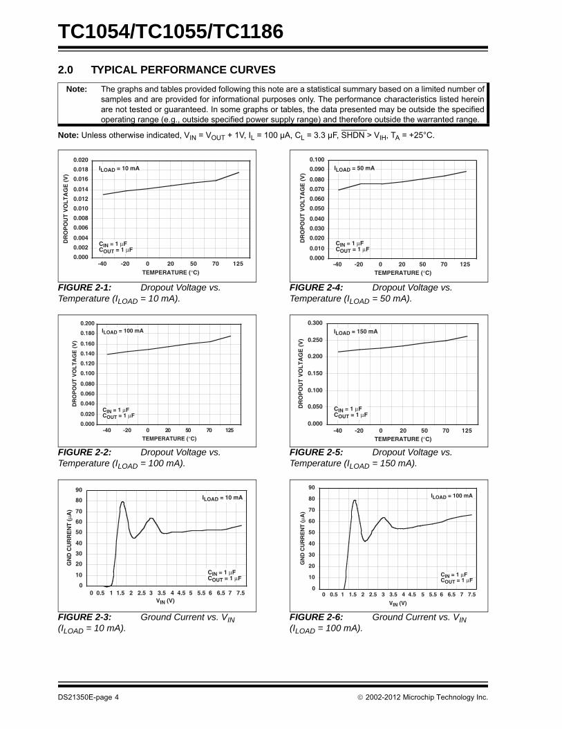
2.0 TYPICAL PERFORMANCE CURVES
Note: Unless otherwise indicated, VIN = VOUT + 1V, IL = 100 µA, CL = 3.3 µF, SHDN > VIH, TA = +25°C.
FIGURE 2-1: Dropout Voltage vs. Temperature (ILOAD = 10 mA).
FIGURE 2-2: Dropout Voltage vs. Temperature (ILOAD = 100 mA).
FIGURE 2-3: Ground Current vs. VIN (ILOAD = 10 mA).
FIGURE 2-4: Dropout Voltage vs. Temperature (ILOAD = 50 mA).
FIGURE 2-5: Dropout Voltage vs. Temperature (ILOAD = 150 mA).
FIGURE 2-6: Ground Current vs. VIN (ILOAD = 100 mA).
Note: The graphs and tables provided following this note are a statistical summary based on a limited number ofsamples and are provided for informational purposes only. The performance characteristics listed hereinare not tested or guaranteed. In some graphs or tables, the data presented may be outside the specifiedoperating range (e.g., outside specified power supply range) and therefore outside the warranted range.
0.000
0.002
0.004
0.006
0.008
0.010
0.012
0.014
0.016
0.018
0.020
-40 -20 0 20 50 70 125
DR
OP
OU
T V
OL
TA
GE
(V
)
ILOAD = 10 mA
CIN = 1 μFCOUT = 1 μF
TEMPERATURE (°C)
0.000
0.020
0.040
0.060
0.080
0.100
0.120
0.140
0.160
0.180
0.200
-40 -20 0 20 50 70 125
DR
OP
OU
T V
OL
TA
GE
(V
)
ILOAD = 100 mA
CIN = 1 μFCOUT = 1 μF
TEMPERATURE (°C)
0
10
20
30
40
50
60
70
80
90
GN
D C
UR
RE
NT
(μA
)
0 0.5 1 1.5 2 2.5 3 3.5 4 4.5 5 5.5 6 6.5 7 7.5
ILOAD = 10 mA
CIN = 1 μFCOUT = 1 μF
VIN (V)
0.000
0.010
0.020
0.030
0.040
0.050
0.060
0.070
0.080
0.090
0.100
-40 -20 0 20 50 70 125
DR
OP
OU
T V
OL
TA
GE
(V
)
ILOAD = 50 mA
CIN = 1 μFCOUT = 1 μF
TEMPERATURE (°C)
0.000
0.050
0.100
0.150
0.200
0.250
0.300
-40 -20 0 20 50 70 125
DR
OP
OU
T V
OL
TA
GE
(V
)
ILOAD = 150 mA
CIN = 1 μFCOUT = 1 μF
TEMPERATURE (°C)
0
10
20
30
40
50
60
70
80
90
GN
D C
UR
RE
NT
(μA
)
0 0.5 1 1.5 2 2.5 3 3.5 4 4.5 5 5.5 6 6.5 7 7.5
ILOAD = 100 mA
CIN = 1 μFCOUT = 1 μF
VIN (V)
DS21350E-page 4 2002-2012 Microchip Technology Inc.
TC1054/TC1055/TC1186
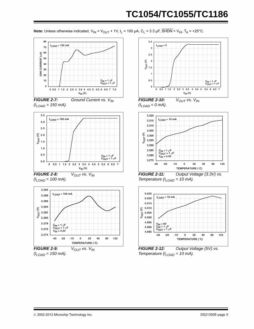
Note: Unless otherwise indicated, VIN = VOUT + 1V, IL = 100 µA, CL = 3.3 µF, SHDN > VIH, TA = +25°C.
FIGURE 2-7: Ground Current vs. VIN (ILOAD = 150 mA).
FIGURE 2-8: VOUT vs. VIN (ILOAD = 100 mA).
FIGURE 2-9: VOUT vs. VIN (ILOAD = 150 mA).
FIGURE 2-10: VOUT vs. VIN (ILOAD = 0 mA).
FIGURE 2-11: Output Voltage (3.3V) vs. Temperature (ILOAD = 10 mA).
FIGURE 2-12: Output Voltage (5V) vs. Temperature (ILOAD = 10 mA).
0
10
20
30
40
50
60
70
80G
ND
CU
RR
EN
T (
μA)
0 0.5 1 1.5 2 2.5 3 3.5 4 4.5 5 5.5 6 6.5 7 7.5
ILOAD = 150 mA
CIN = 1 μFCOUT = 1 μF
VIN (V)
0.0
0.5
1.0
1.5
2.0
2.5
3.0
3.5ILOAD = 100 mA
CIN = 1 μFCOUT = 1 μF
0 0.5 1 1.5 2 2.5 3 3.5 4 4.5 5 5.5 6 6.5 7VIN (V)
VO
UT (
V)
3.274
3.276
3.278
3.280
3.282
3.284
3.286
3.288
3.290
-40 -20 -10 0 20 40 85 125
ILOAD = 150 mA
CIN = 1 μFCOUT = 1 μFVIN = 4.3V
TEMPERATURE (°C)
VO
UT (
V)
0
0.5
1
1.5
2
2.5
3
3.5
0 0.5 1 1.5 2 2.5 3 3.5 4 4.5 5 5.5 6 6.5 7
ILOAD = 0
CIN = 1 μFCOUT = 1 μF
VIN (V)
VO
UT (
V)
3.275
3.280
3.285
3.290
3.295
3.300
3.305
3.310
3.315
3.320
-40 -20 -10 0 20 40 85 125
ILOAD = 10 mA
CIN = 1 μFCOUT = 1 μFVIN = 4.3V
TEMPERATURE (°C)
VO
UT (
V)
4.985
4.990
4.995
5.000
5.005
5.010
5.015
5.020
5.025
-40 -20 -10 0 20 40 85 125
ILOAD = 10 mA
VIN = 6VCIN = 1 μFCOUT = 1 μF
TEMPERATURE (°C)
VO
UT (
V)
2002-2012 Microchip Technology Inc. DS21350E-page 5
TC1054/TC1055/TC1186
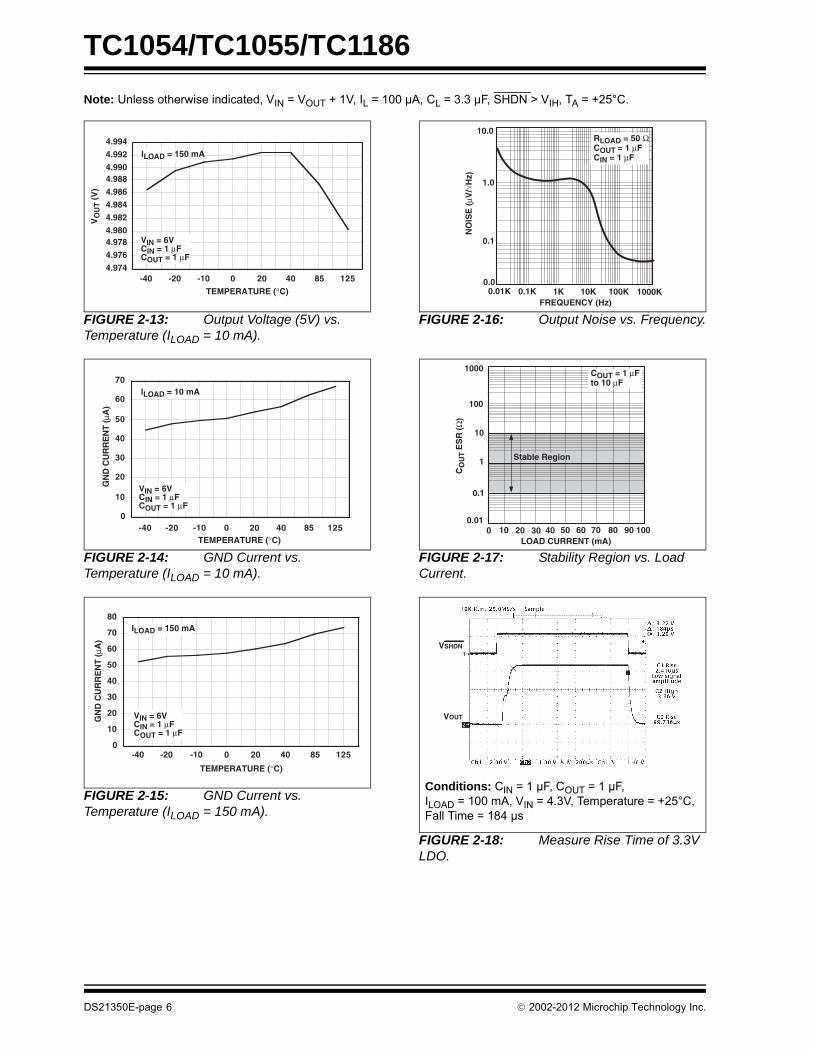
Note: Unless otherwise indicated, VIN = VOUT + 1V, IL = 100 µA, CL = 3.3 µF, SHDN > VIH, TA = +25°C.
FIGURE 2-13: Output Voltage (5V) vs. Temperature (ILOAD = 10 mA).
FIGURE 2-14: GND Current vs. Temperature (ILOAD = 10 mA).
FIGURE 2-15: GND Current vs. Temperature (ILOAD = 150 mA).
FIGURE 2-16: Output Noise vs. Frequency.
FIGURE 2-17: Stability Region vs. Load Current.
FIGURE 2-18: Measure Rise Time of 3.3V LDO.
4.974
4.976
4.9784.980
4.982
4.984
4.986
4.9884.990
4.992
4.994
-40 -20 -10 0 20 40 85 125
ILOAD = 150 mA
VIN = 6VCIN = 1 μFCOUT = 1 μF
TEMPERATURE (°C)
VO
UT (
V)
0
10
20
30
40
50
60
70
-40 -20 -10 0 20 40 85 125
GN
D C
UR
RE
NT
(μA
)
ILOAD = 10 mA
VIN = 6VCIN = 1 μFCOUT = 1 μF
TEMPERATURE (°C)
0
10
20
30
40
50
60
70
80
-40 -20 -10 0 20 40 85 125
GN
D C
UR
RE
NT
(μA
)
ILOAD = 150 mA
VIN = 6VCIN = 1 μFCOUT = 1 μF
TEMPERATURE (°C)
10.0
1.0
0.1
0.00.01K 0.1K 1K 10K 100K 1000K
FREQUENCY (Hz)
NO
ISE
(μV
/√H
z)
RLOAD = 50 Ω COUT = 1 μFCIN = 1 μF
1000
100
10
1
0.1
0.010 10 20 30 40 50 60 70 80 90 100
LOAD CURRENT (mA)
CO
UT
ES
R (Ω
)
COUT = 1 μF to 10 μF
Stable Region
VSHDN
VOUT
Conditions: CIN = 1 µF, COUT = 1 µF,ILOAD = 100 mA, VIN = 4.3V, Temperature = +25°C,Fall Time = 184 µs
DS21350E-page 6 2002-2012 Microchip Technology Inc.
TC1054/TC1055/TC1186
Note: Unless otherwise indicated, VIN = VOUT + 1V, IL = 100 µA, CL = 3.3 µF, SHDN > VIH, TA = +25°C.
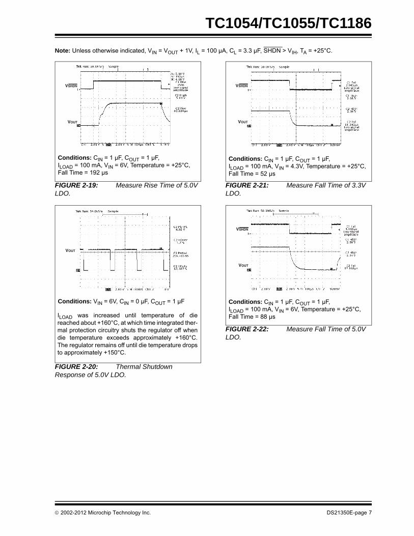
FIGURE 2-19: Measure Rise Time of 5.0V LDO.
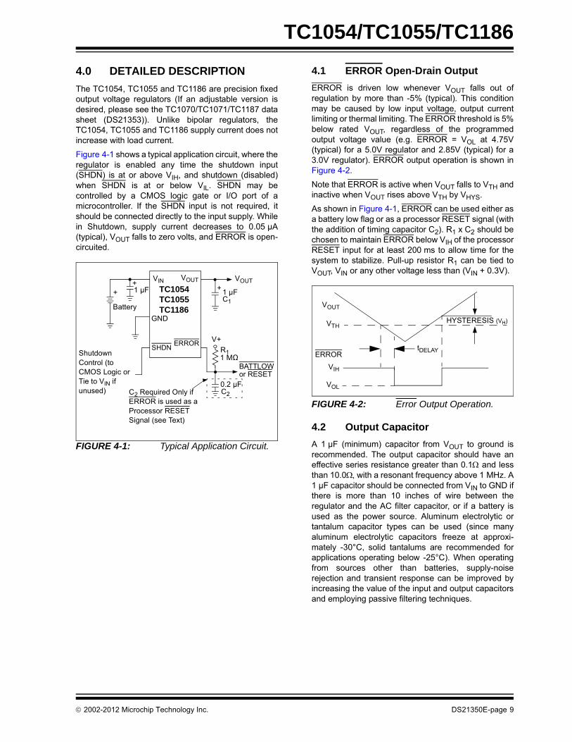
FIGURE 2-20: Thermal Shutdown Response of 5.0V LDO.
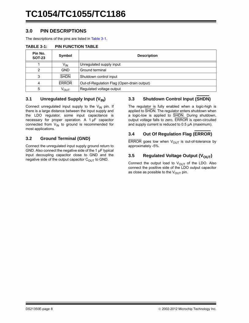
FIGURE 2-21: Measure Fall Time of 3.3V LDO.
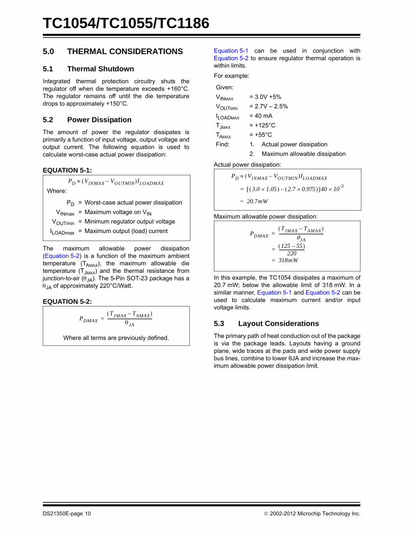
FIGURE 2-22: Measure Fall Time of 5.0V LDO.
VSHDN
VOUT
Conditions: CIN = 1 µF, COUT = 1 µF,ILOAD = 100 mA, VIN = 6V, Temperature = +25°C,Fall Time = 192 µs
VOUT
Conditions: VIN = 6V, CIN = 0 µF, COUT = 1 µF
ILOAD was increased until temperature of diereached about +160°C, at which time integrated ther-mal protection circuitry shuts the regulator off whendie temperature exceeds approximately +160°C.The regulator remains off until die temperature dropsto approximately +150°C.
VSHDN
VOUT
Conditions: CIN = 1 µF, COUT = 1 µF,ILOAD = 100 mA, VIN = 4.3V, Temperature = +25°C,Fall Time = 52 µs
VSHDN
VOUT
Conditions: CIN = 1 µF, COUT = 1 µF,ILOAD = 100 mA, VIN = 6V, Temperature = +25°C,Fall Time = 88 µs
2002-2012 Microchip Technology Inc. DS21350E-page 7
TC1054/TC1055/TC1186
3.0 PIN DESCRIPTIONS
The descriptions of the pins are listed in Table 3-1.
3.1 Unregulated Supply Input (VIN)
Connect unregulated input supply to the VIN pin. Ifthere is a large distance between the input supply andthe LDO regulator, some input capacitance isnecessary for proper operation. A 1 µF capacitorconnected from VIN to ground is recommended formost applications.
3.2 Ground Terminal (GND)
Connect the unregulated input supply ground return toGND. Also connect the negative side of the 1 µF typicalinput decoupling capacitor close to GND and thenegative side of the output capacitor COUT to GND.
3.3 Shutdown Control Input (SHDN)
The regulator is fully enabled when a logic-high isapplied to SHDN. The regulator enters shutdown whena logic-low is applied to SHDN. During shutdown,output voltage falls to zero, ERROR is open-circuitedand supply current is reduced to 0.5 µA (maximum).
3.4 Out Of Regulation Flag (ERROR)
ERROR goes low when VOUT is out-of-tolerance byapproximately -5%.
3.5 Regulated Voltage Output (VOUT)
Connect the output load to VOUT of the LDO. Alsoconnect the positive side of the LDO output capacitoras close as possible to the VOUT pin.
TABLE 3-1: PIN FUNCTION TABLE
Pin No.SOT-23
Symbol Description
1 VIN Unregulated supply input
2 GND Ground terminal
3 SHDN Shutdown control input
4 ERROR Out-of-Regulation Flag (Open-drain output)
5 VOUT Regulated voltage output
DS21350E-page 8 2002-2012 Microchip Technology Inc.
TC1054/TC1055/TC1186
4.0 DETAILED DESCRIPTION
The TC1054, TC1055 and TC1186 are precision fixedoutput voltage regulators (If an adjustable version isdesired, please see the TC1070/TC1071/TC1187 datasheet (DS21353)). Unlike bipolar regulators, theTC1054, TC1055 and TC1186 supply current does notincrease with load current.
Figure 4-1 shows a typical application circuit, where theregulator is enabled any time the shutdown input(SHDN) is at or above VIH, and shutdown (disabled)when SHDN is at or below VIL. SHDN may becontrolled by a CMOS logic gate or I/O port of amicrocontroller. If the SHDN input is not required, itshould be connected directly to the input supply. Whilein Shutdown, supply current decreases to 0.05 µA(typical), VOUT falls to zero volts, and ERROR is open-circuited.
FIGURE 4-1: Typical Application Circuit.
4.1 ERROR Open-Drain Output
ERROR is driven low whenever VOUT falls out ofregulation by more than -5% (typical). This conditionmay be caused by low input voltage, output currentlimiting or thermal limiting. The ERROR threshold is 5%below rated VOUT, regardless of the programmedoutput voltage value (e.g. ERROR = VOL at 4.75V(typical) for a 5.0V regulator and 2.85V (typical) for a3.0V regulator). ERROR output operation is shown inFigure 4-2.
Note that ERROR is active when VOUT falls to VTH andinactive when VOUT rises above VTH by VHYS.
As shown in Figure 4-1, ERROR can be used either asa battery low flag or as a processor RESET signal (withthe addition of timing capacitor C2). R1 x C2 should bechosen to maintain ERROR below VIH of the processorRESET input for at least 200 ms to allow time for thesystem to stabilize. Pull-up resistor R1 can be tied toVOUT, VIN or any other voltage less than (VIN + 0.3V).
FIGURE 4-2: Error Output Operation.
4.2 Output Capacitor
A 1 µF (minimum) capacitor from VOUT to ground isrecommended. The output capacitor should have aneffective series resistance greater than 0.1 and lessthan 10.0, with a resonant frequency above 1 MHz. A1 µF capacitor should be connected from VIN to GND ifthere is more than 10 inches of wire between theregulator and the AC filter capacitor, or if a battery isused as the power source. Aluminum electrolytic ortantalum capacitor types can be used (since manyaluminum electrolytic capacitors freeze at approxi-mately -30°C, solid tantalums are recommended forapplications operating below -25°C). When operatingfrom sources other than batteries, supply-noiserejection and transient response can be improved byincreasing the value of the input and output capacitorsand employing passive filtering techniques.
or RESET
VOUT
SHDN
GND
ERROR
+VIN VOUT
1 µF+
Battery
+
0.2 µFC2
R1 1 MΩ
V+
BATTLOW
1 µFC1
TC1054TC1055TC1186
C2 Required Only if ERROR is used as a Processor RESET Signal (see Text)
Shutdown Control (to CMOS Logic or Tie to VIN if unused)
VTH
VOUT
ERROR
VIH
VOL
HYSTERESIS (VH)
tDELAY
2002-2012 Microchip Technology Inc. DS21350E-page 9
TC1054/TC1055/TC1186
5.0 THERMAL CONSIDERATIONS
5.1 Thermal Shutdown
Integrated thermal protection circuitry shuts theregulator off when die temperature exceeds +160°C.The regulator remains off until the die temperaturedrops to approximately +150°C.
5.2 Power Dissipation
The amount of power the regulator dissipates isprimarily a function of input voltage, output voltage andoutput current. The following equation is used tocalculate worst-case actual power dissipation:
EQUATION 5-1:
The maximum allowable power dissipation(Equation 5-2) is a function of the maximum ambienttemperature (TAMAX), the maximum allowable dietemperature (TJMAX) and the thermal resistance fromjunction-to-air (JA). The 5-Pin SOT-23 package has aJA of approximately 220°C/Watt.
EQUATION 5-2:
Equation 5-1 can be used in conjunction withEquation 5-2 to ensure regulator thermal operation iswithin limits.
For example:
Actual power dissipation:
Maximum allowable power dissipation:
In this example, the TC1054 dissipates a maximum of20.7 mW; below the allowable limit of 318 mW. In asimilar manner, Equation 5-1 and Equation 5-2 can beused to calculate maximum current and/or inputvoltage limits.
5.3 Layout Considerations
The primary path of heat conduction out of the packageis via the package leads. Layouts having a groundplane, wide traces at the pads and wide power supplybus lines, combine to lower θJA and increase the max-imum allowable power dissipation limit.
PD VINMAX VOUTMIN– ILOADMAX
Where:
PD = Worst-case actual power dissipation
VINmax = Maximum voltage on VIN
VOUTmin = Minimum regulator output voltage
ILOADmax = Maximum output (load) current
Where all terms are previously defined.
PDMAX
TJMAX TAMAX– JA
--------------------------------------------=
Given:
VINMAX = 3.0V +5%
VOUTMIN = 2.7V – 2.5%
ILOADMAX = 40 mA
TJMAX = +125°C
TAMAX = +55°C
Find: 1. Actual power dissipation
2. Maximum allowable dissipation
PD VINMAX VOUTMIN– ILOADMAX
3.0 1.05 2.7 0.975 – 40 10-3=
20.7mW=
PDMAX
TJMAX TAMAX– JA
--------------------------------------------=
125 55– 220
-------------------------=
318mW=
DS21350E-page 10 2002-2012 Microchip Technology Inc.
TC1054/TC1055/TC1186
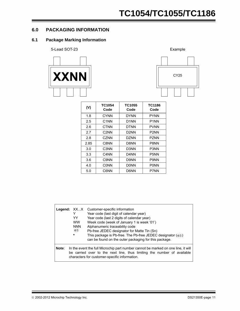
6.0 PACKAGING INFORMATION
6.1 Package Marking Information
Legend: XX...X Customer-specific informationY Year code (last digit of calendar year)YY Year code (last 2 digits of calendar year)WW Week code (week of January 1 is week ‘01’)NNN Alphanumeric traceability code Pb-free JEDEC designator for Matte Tin (Sn)* This package is Pb-free. The Pb-free JEDEC designator ( )
can be found on the outer packaging for this package.
3e
3e
Note: In the event the full Microchip part number cannot be marked on one line, it willbe carried over to the next line, thus limiting the number of availablecharacters for customer-specific information.
5-Lead SOT-23 Example
XXNN CY25
(V)TC1054Code
TC1055Code
TC1186Code
1.8 CYNN DYNN PYNN
2.5 C1NN D1NN P1NN
2.6 CTNN DTNN PVNN
2.7 C2NN D2NN P2NN
2.8 CZNN DZNN PZNN
2.85 C8NN D8NN P8NN
3.0 C3NN D3NN P3NN
3.3 C4NN D4NN P5NN
3.6 C9NN D9NN P9NN
4.0 C0NN D0NN P0NN
5.0 C6NN D6NN P7NN
2002-2012 Microchip Technology Inc. DS21350E-page 11
TC1054/TC1055/TC1186
!!"#"$%" "&!$%!!"&!$%!!!$'" !" !"$#(
)*+ )! ! $'$,%!--$%$$!
.$ !$%$/"-!0!!$1/&$$"$$$+22--- 2/
3$! 44# # !4 $! 5 56 7
5% 8&1! 5 4"1$ )*6%$!"4"1$ )*6,9$ : ""1/ /!! ; : $"&& : 6,<"$ # : ""1/<"$ # : ;6,4$ : .$4$ 4 : =.$$ 4 : ;.$ > : >4" /!! ; : =4"<"$ 8 :
φ
Nb
E
E1
D
1 2 3
e
e1
A
A1
A2 c
L
L1
- *)
DS21350E-page 12 2002-2012 Microchip Technology Inc.
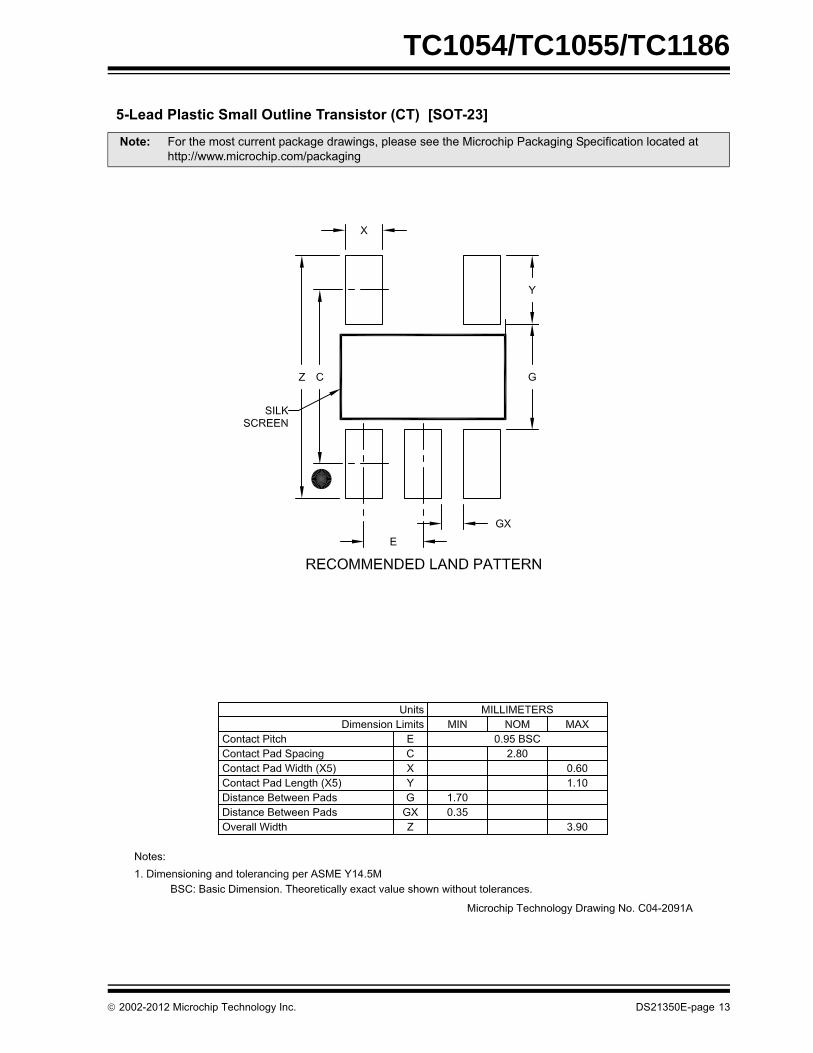
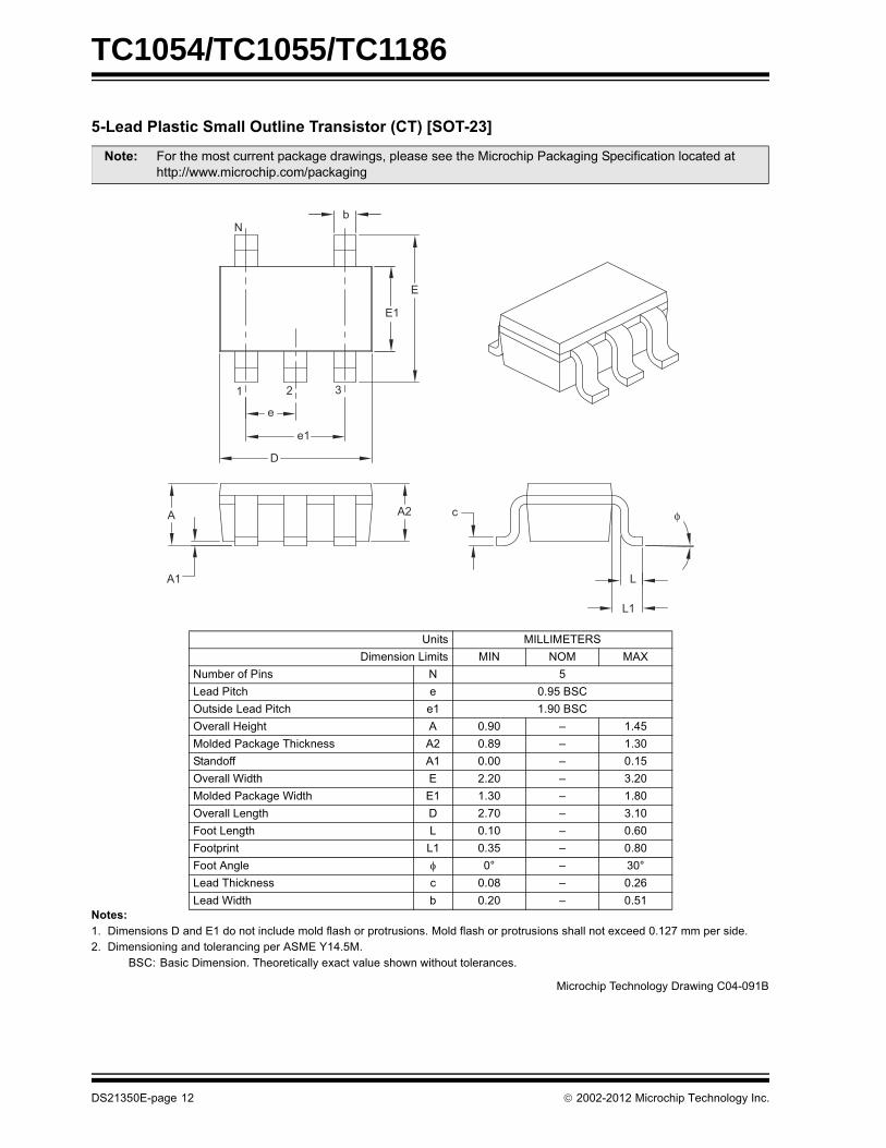
TC1054/TC1055/TC1186
5-Lead Plastic Small Outline Transistor (CT) [SOT-23]
Note: For the most current package drawings, please see the Microchip Packaging Specification located at http://www.microchip.com/packaging
2002-2012 Microchip Technology Inc. DS21350E-page 13
TC1054/TC1055/TC1186
NOTES:
DS21350E-page 14 2002-2012 Microchip Technology Inc.
TC1054/TC1055/TC1186
APPENDIX A: REVISION HISTORY
Revision E (December 2012)
The following is the list of modifications:
1. Updated the Input Voltage value in AbsoluteMaximum Ratings † section.
2. Updated Section 6.0, Packaging Information.
3. Updated Product Identification System.
Revision D (February 2007)
• Corrected standard output voltages on page 1 and in Section , Product Identification System.
• Added TDELAY parameter in DC Characteristics table in Section 1.0, Electrical Characteristics.
• Changes to Figure 4-2.
• Section 6.0, Packaging Information: Corrected SOT-23 Packaging Information.
Revision C (March 2003)
• Undocumented changes.
Revision B (May 2002)
• Undocumented changes.
Revision A (March 2002)
• Original Release of this Document.
2002-2012 Microchip Technology Inc. DS21350E-page 15

TC1054/TC1055/TC1186
NOTES:
DS21350E-page 16 2002-2012 Microchip Technology Inc.
TC1054/TC1055/TC1186
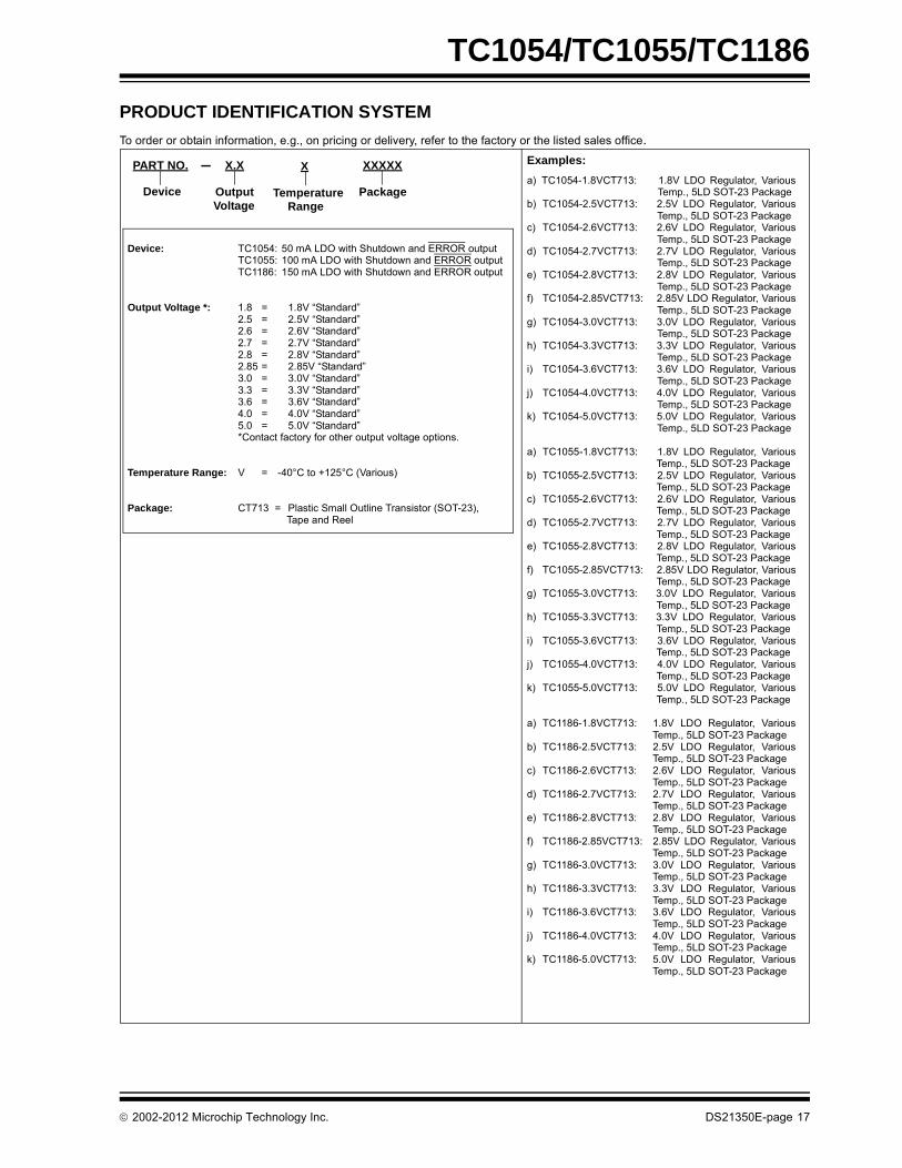
PRODUCT IDENTIFICATION SYSTEM
To order or obtain information, e.g., on pricing or delivery, refer to the factory or the listed sales office.
Device: TC1054: 50 mA LDO with Shutdown and ERROR output
TC1055: 100 mA LDO with Shutdown and ERROR outputTC1186: 150 mA LDO with Shutdown and ERROR output
Output Voltage *: 1.8 = 1.8V “Standard”2.5 = 2.5V “Standard”2.6 = 2.6V “Standard”2.7 = 2.7V “Standard”2.8 = 2.8V “Standard”2.85 = 2.85V “Standard”3.0 = 3.0V “Standard”3.3 = 3.3V “Standard”3.6 = 3.6V “Standard”4.0 = 4.0V “Standard”5.0 = 5.0V “Standard”*Contact factory for other output voltage options.
Temperature Range: V = -40°C to +125°C (Various)
Package: CT713 = Plastic Small Outline Transistor (SOT-23), Tape and Reel
PART NO. X.X XXXXX
PackageOutputVoltage
Device
Examples:
a) TC1054-1.8VCT713: 1.8V LDO Regulator, VariousTemp., 5LD SOT-23 Package
b) TC1054-2.5VCT713: 2.5V LDO Regulator, VariousTemp., 5LD SOT-23 Package
c) TC1054-2.6VCT713: 2.6V LDO Regulator, VariousTemp., 5LD SOT-23 Package
d) TC1054-2.7VCT713: 2.7V LDO Regulator, VariousTemp., 5LD SOT-23 Package
e) TC1054-2.8VCT713: 2.8V LDO Regulator, VariousTemp., 5LD SOT-23 Package
f) TC1054-2.85VCT713: 2.85V LDO Regulator, VariousTemp., 5LD SOT-23 Package
g) TC1054-3.0VCT713: 3.0V LDO Regulator, VariousTemp., 5LD SOT-23 Package
h) TC1054-3.3VCT713: 3.3V LDO Regulator, VariousTemp., 5LD SOT-23 Package
i) TC1054-3.6VCT713: 3.6V LDO Regulator, VariousTemp., 5LD SOT-23 Package
j) TC1054-4.0VCT713: 4.0V LDO Regulator, VariousTemp., 5LD SOT-23 Package
k) TC1054-5.0VCT713: 5.0V LDO Regulator, VariousTemp., 5LD SOT-23 Package
a) TC1055-1.8VCT713: 1.8V LDO Regulator, VariousTemp., 5LD SOT-23 Package
b) TC1055-2.5VCT713: 2.5V LDO Regulator, VariousTemp., 5LD SOT-23 Package
c) TC1055-2.6VCT713: 2.6V LDO Regulator, VariousTemp., 5LD SOT-23 Package
d) TC1055-2.7VCT713: 2.7V LDO Regulator, VariousTemp., 5LD SOT-23 Package
e) TC1055-2.8VCT713: 2.8V LDO Regulator, VariousTemp., 5LD SOT-23 Package
f) TC1055-2.85VCT713: 2.85V LDO Regulator, VariousTemp., 5LD SOT-23 Package
g) TC1055-3.0VCT713: 3.0V LDO Regulator, VariousTemp., 5LD SOT-23 Package
h) TC1055-3.3VCT713: 3.3V LDO Regulator, VariousTemp., 5LD SOT-23 Package
i) TC1055-3.6VCT713: 3.6V LDO Regulator, VariousTemp., 5LD SOT-23 Package
j) TC1055-4.0VCT713: 4.0V LDO Regulator, VariousTemp., 5LD SOT-23 Package
k) TC1055-5.0VCT713: 5.0V LDO Regulator, VariousTemp., 5LD SOT-23 Package
a) TC1186-1.8VCT713: 1.8V LDO Regulator, VariousTemp., 5LD SOT-23 Package
b) TC1186-2.5VCT713: 2.5V LDO Regulator, VariousTemp., 5LD SOT-23 Package
c) TC1186-2.6VCT713: 2.6V LDO Regulator, VariousTemp., 5LD SOT-23 Package
d) TC1186-2.7VCT713: 2.7V LDO Regulator, VariousTemp., 5LD SOT-23 Package
e) TC1186-2.8VCT713: 2.8V LDO Regulator, VariousTemp., 5LD SOT-23 Package
f) TC1186-2.85VCT713: 2.85V LDO Regulator, VariousTemp., 5LD SOT-23 Package
g) TC1186-3.0VCT713: 3.0V LDO Regulator, VariousTemp., 5LD SOT-23 Package
h) TC1186-3.3VCT713: 3.3V LDO Regulator, VariousTemp., 5LD SOT-23 Package
i) TC1186-3.6VCT713: 3.6V LDO Regulator, VariousTemp., 5LD SOT-23 Package
j) TC1186-4.0VCT713: 4.0V LDO Regulator, VariousTemp., 5LD SOT-23 Package
k) TC1186-5.0VCT713: 5.0V LDO Regulator, VariousTemp., 5LD SOT-23 Package
X
TemperatureRange
2002-2012 Microchip Technology Inc. DS21350E-page 17

TC1054/TC1055/TC1186
NOTES:
DS21350E-page 18 2002-2012 Microchip Technology Inc.
Note the following details of the code protection feature on Microchip devices:
• Microchip products meet the specification contained in their particular Microchip Data Sheet.
• Microchip believes that its family of products is one of the most secure families of its kind on the market today, when used in the intended manner and under normal conditions.
• There are dishonest and possibly illegal methods used to breach the code protection feature. All of these methods, to our knowledge, require using the Microchip products in a manner outside the operating specifications contained in Microchip’s Data Sheets. Most likely, the person doing so is engaged in theft of intellectual property.
• Microchip is willing to work with the customer who is concerned about the integrity of their code.
• Neither Microchip nor any other semiconductor manufacturer can guarantee the security of their code. Code protection does not mean that we are guaranteeing the product as “unbreakable.”
Code protection is constantly evolving. We at Microchip are committed to continuously improving the code protection features of ourproducts. Attempts to break Microchip’s code protection feature may be a violation of the Digital Millennium Copyright Act. If such actsallow unauthorized access to your software or other copyrighted work, you may have a right to sue for relief under that Act.
Information contained in this publication regarding deviceapplications and the like is provided only for your convenienceand may be superseded by updates. It is your responsibility toensure that your application meets with your specifications.MICROCHIP MAKES NO REPRESENTATIONS ORWARRANTIES OF ANY KIND WHETHER EXPRESS ORIMPLIED, WRITTEN OR ORAL, STATUTORY OROTHERWISE, RELATED TO THE INFORMATION,INCLUDING BUT NOT LIMITED TO ITS CONDITION,QUALITY, PERFORMANCE, MERCHANTABILITY ORFITNESS FOR PURPOSE. Microchip disclaims all liabilityarising from this information and its use. Use of Microchipdevices in life support and/or safety applications is entirely atthe buyer’s risk, and the buyer agrees to defend, indemnify andhold harmless Microchip from any and all damages, claims,suits, or expenses resulting from such use. No licenses areconveyed, implicitly or otherwise, under any Microchipintellectual property rights.
2002-2012 Microchip Technology Inc.
QUALITY MANAGEMENT SYSTEM CERTIFIED BY DNV
== ISO/TS 16949 ==
Trademarks
The Microchip name and logo, the Microchip logo, dsPIC, FlashFlex, KEELOQ, KEELOQ logo, MPLAB, PIC, PICmicro, PICSTART, PIC32 logo, rfPIC, SST, SST Logo, SuperFlash and UNI/O are registered trademarks of Microchip Technology Incorporated in the U.S.A. and other countries.
FilterLab, Hampshire, HI-TECH C, Linear Active Thermistor, MTP, SEEVAL and The Embedded Control Solutions Company are registered trademarks of Microchip Technology Incorporated in the U.S.A.
Silicon Storage Technology is a registered trademark of Microchip Technology Inc. in other countries.
Analog-for-the-Digital Age, Application Maestro, BodyCom, chipKIT, chipKIT logo, CodeGuard, dsPICDEM, dsPICDEM.net, dsPICworks, dsSPEAK, ECAN, ECONOMONITOR, FanSense, HI-TIDE, In-Circuit Serial Programming, ICSP, Mindi, MiWi, MPASM, MPF, MPLAB Certified logo, MPLIB, MPLINK, mTouch, Omniscient Code Generation, PICC, PICC-18, PICDEM, PICDEM.net, PICkit, PICtail, REAL ICE, rfLAB, Select Mode, SQI, Serial Quad I/O, Total Endurance, TSHARC, UniWinDriver, WiperLock, ZENA and Z-Scale are trademarks of Microchip Technology Incorporated in the U.S.A. and other countries.
SQTP is a service mark of Microchip Technology Incorporated in the U.S.A.
GestIC and ULPP are registered trademarks of Microchip Technology Germany II GmbH & Co. & KG, a subsidiary of Microchip Technology Inc., in other countries.
All other trademarks mentioned herein are property of their respective companies.
© 2002-2012, Microchip Technology Incorporated, Printed in the U.S.A., All Rights Reserved.
Printed on recycled paper.
ISBN: 978-1-62076-721-4
Microchip received ISO/TS-16949:2009 certification for its worldwide
DS21350E-page 19
headquarters, design and wafer fabrication facilities in Chandler and Tempe, Arizona; Gresham, Oregon and design centers in California and India. The Company’s quality system processes and procedures are for its PIC® MCUs and dsPIC® DSCs, KEELOQ® code hopping devices, Serial EEPROMs, microperipherals, nonvolatile memory and analog products. In addition, Microchip’s quality system for the design and manufacture of development systems is ISO 9001:2000 certified.
DS21350E-page 20 2002-2012 Microchip Technology Inc.
AMERICASCorporate Office2355 West Chandler Blvd.Chandler, AZ 85224-6199Tel: 480-792-7200 Fax: 480-792-7277Technical Support: http://www.microchip.com/supportWeb Address: www.microchip.com
AtlantaDuluth, GA Tel: 678-957-9614 Fax: 678-957-1455
BostonWestborough, MA Tel: 774-760-0087 Fax: 774-760-0088
ChicagoItasca, IL Tel: 630-285-0071 Fax: 630-285-0075
ClevelandIndependence, OH Tel: 216-447-0464 Fax: 216-447-0643
DallasAddison, TX Tel: 972-818-7423 Fax: 972-818-2924
DetroitFarmington Hills, MI Tel: 248-538-2250Fax: 248-538-2260
IndianapolisNoblesville, IN Tel: 317-773-8323Fax: 317-773-5453
Los AngelesMission Viejo, CA Tel: 949-462-9523 Fax: 949-462-9608
Santa ClaraSanta Clara, CA Tel: 408-961-6444Fax: 408-961-6445
TorontoMississauga, Ontario, CanadaTel: 905-673-0699 Fax: 905-673-6509
ASIA/PACIFICAsia Pacific OfficeSuites 3707-14, 37th FloorTower 6, The GatewayHarbour City, KowloonHong KongTel: 852-2401-1200Fax: 852-2401-3431
Australia - SydneyTel: 61-2-9868-6733Fax: 61-2-9868-6755
China - BeijingTel: 86-10-8569-7000 Fax: 86-10-8528-2104
China - ChengduTel: 86-28-8665-5511Fax: 86-28-8665-7889
China - ChongqingTel: 86-23-8980-9588Fax: 86-23-8980-9500
China - HangzhouTel: 86-571-2819-3187 Fax: 86-571-2819-3189
China - Hong Kong SARTel: 852-2943-5100 Fax: 852-2401-3431
China - NanjingTel: 86-25-8473-2460Fax: 86-25-8473-2470
China - QingdaoTel: 86-532-8502-7355Fax: 86-532-8502-7205
China - ShanghaiTel: 86-21-5407-5533 Fax: 86-21-5407-5066
China - ShenyangTel: 86-24-2334-2829Fax: 86-24-2334-2393
China - ShenzhenTel: 86-755-8864-2200 Fax: 86-755-8203-1760
China - WuhanTel: 86-27-5980-5300Fax: 86-27-5980-5118
China - XianTel: 86-29-8833-7252Fax: 86-29-8833-7256
China - XiamenTel: 86-592-2388138 Fax: 86-592-2388130
China - ZhuhaiTel: 86-756-3210040 Fax: 86-756-3210049
ASIA/PACIFICIndia - BangaloreTel: 91-80-3090-4444 Fax: 91-80-3090-4123
India - New DelhiTel: 91-11-4160-8631Fax: 91-11-4160-8632
India - PuneTel: 91-20-2566-1512Fax: 91-20-2566-1513
Japan - OsakaTel: 81-6-6152-7160 Fax: 81-6-6152-9310
Japan - TokyoTel: 81-3-6880- 3770 Fax: 81-3-6880-3771
Korea - DaeguTel: 82-53-744-4301Fax: 82-53-744-4302
Korea - SeoulTel: 82-2-554-7200Fax: 82-2-558-5932 or 82-2-558-5934
Malaysia - Kuala LumpurTel: 60-3-6201-9857Fax: 60-3-6201-9859
Malaysia - PenangTel: 60-4-227-8870Fax: 60-4-227-4068
Philippines - ManilaTel: 63-2-634-9065Fax: 63-2-634-9069
SingaporeTel: 65-6334-8870Fax: 65-6334-8850
Taiwan - Hsin ChuTel: 886-3-5778-366Fax: 886-3-5770-955
Taiwan - KaohsiungTel: 886-7-213-7828Fax: 886-7-330-9305
Taiwan - TaipeiTel: 886-2-2508-8600 Fax: 886-2-2508-0102
Thailand - BangkokTel: 66-2-694-1351Fax: 66-2-694-1350
EUROPEAustria - WelsTel: 43-7242-2244-39Fax: 43-7242-2244-393Denmark - CopenhagenTel: 45-4450-2828 Fax: 45-4485-2829
France - ParisTel: 33-1-69-53-63-20 Fax: 33-1-69-30-90-79
Germany - MunichTel: 49-89-627-144-0 Fax: 49-89-627-144-44
Italy - Milan Tel: 39-0331-742611 Fax: 39-0331-466781
Netherlands - DrunenTel: 31-416-690399 Fax: 31-416-690340
Spain - MadridTel: 34-91-708-08-90Fax: 34-91-708-08-91
UK - WokinghamTel: 44-118-921-5869Fax: 44-118-921-5820
Worldwide Sales and Service
11/29/12