Embed Size (px)
Citation preview
8/3/2019 Tatler, Sep 2011
http://slidepdf.com/reader/full/tatler-sep-2011 1/4
High Performance Electrolyte GatedCarbon Nanotube Transistors
Sami Rosenblatt,† Yuval Yaish,† Jiwoong Park,†,‡ Jeff Gore,‡ Vera Sazonova,† andPaul L. McEuen*,†
Laboratory of Atomic and Solid State Physics, Cornell UniVersity,
Ithaca, New York 14853 and Department of Physics, UniVersity of California,
Berkeley, California 94720
Received June 7, 2002
ABSTRACT
We have fabricated high performance field-effect transistors made from semiconducting single-walled carbon nanotubes (SWNTs). Using
chemical vapor deposition to grow the tubes, annealing to improve the contacts, and an electrolyte as a gate, we obtain very high device
mobilities and transconductances. These measurements demonstrate that SWNTs are attractive for both electronic applications and for chemical
and biological sensing.
Field effect transistors (FETs) made from semiconducting
single-walled carbon nanotubes (SWNTs) have been in-
tensely investigated1-6 since they were first made in 1998.7
The reported properties of SWNT transistors have varied
widely due to variations in the quality of the nanotube
material, the device geometry, and the contacts. Optimizing
their properties is crucial for applications in both electronics
and in chemical and biological sensing. For electronic
applications, a number of parameters dictate the performance
of an FET, such as mobility and transconductance. For
sensing,8,9 the ability to work in the appropriate environment
(e.g., salty water for biological applications) is critical. Here
we report on optimized SWNT transistors where an elec-
trolyte solution is used as a gate. The high mobilities, low
contact resistances, and excellent gate coupling of these
devices yield device characteristics that significantly exceed
previous reports. They show that SWNT transistors are very
attractive for both electronics and molecular sensing.
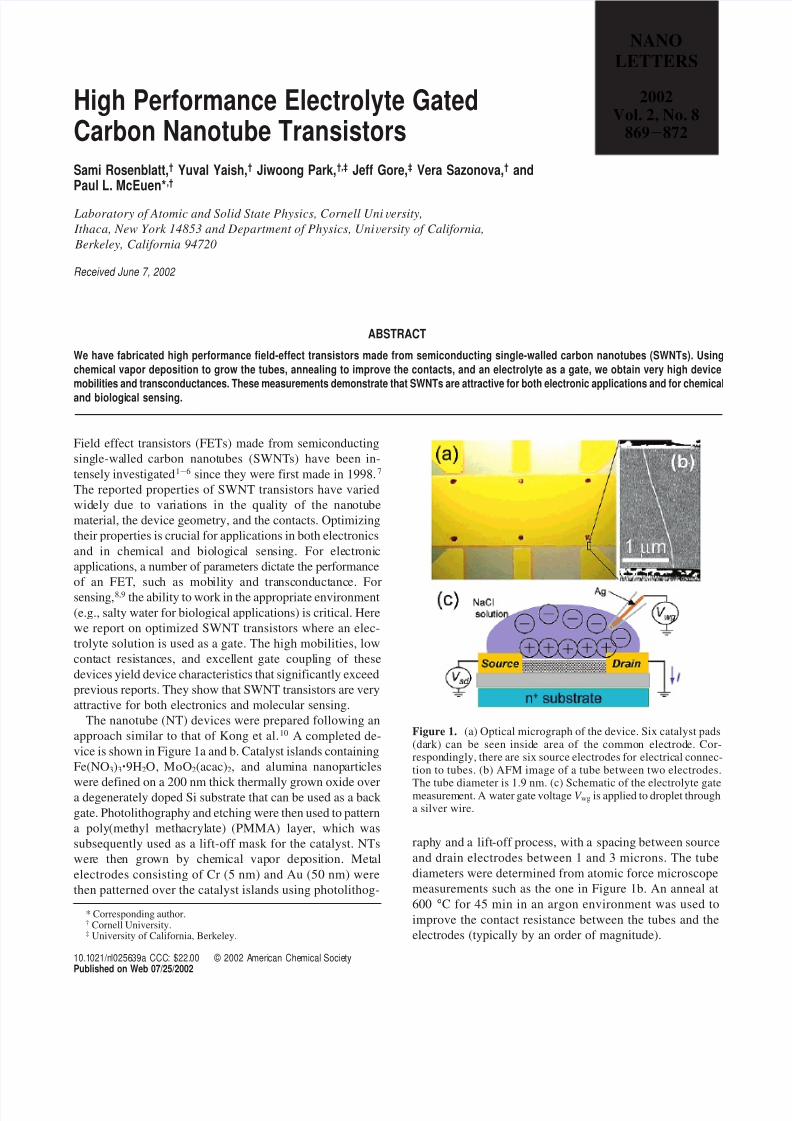
The nanotube (NT) devices were prepared following an
approach similar to that of Kong et al.10 A completed de-
vice is shown in Figure 1a and b. Catalyst islands containing
Fe(NO3)3‚9H2O, MoO2(acac)2, and alumina nanoparticles
were defined on a 200 nm thick thermally grown oxide overa degenerately doped Si substrate that can be used as a back
gate. Photolithography and etching were then used to pattern
a poly(methyl methacrylate) (PMMA) layer, which was
subsequently used as a lift-off mask for the catalyst. NTs
were then grown by chemical vapor deposition. Metal
electrodes consisting of Cr (5 nm) and Au (50 nm) were
then patterned over the catalyst islands using photolithog-
raphy and a lift-off process, with a spacing between source
and drain electrodes between 1 and 3 microns. The tube
diameters were determined from atomic force microscope
measurements such as the one in Figure 1b. An anneal at
600 °C for 45 min in an argon environment was used to
improve the contact resistance between the tubes and the
electrodes (typically by an order of magnitude).
* Corresponding author.† Cornell University.‡ University of California, Berkeley.
Figure 1. (a) Optical micrograph of the device. Six catalyst pads(dark) can be seen inside area of the common electrode. Cor-respondingly, there are six source electrodes for electrical connec-tion to tubes. (b) AFM image of a tube between two electrodes.
The tube diameter is 1.9 nm. (c) Schematic of the electrolyte gatemeasurement. A water gate voltage V wg is applied to droplet througha silver wire.
NANO
LETTERS
2002Vol. 2, No. 8
869-872
10.1021/nl025639a CCC: $22.00 © 2002 American Chemical SocietyPublished on Web 07/25/2002
8/3/2019 Tatler, Sep 2011
http://slidepdf.com/reader/full/tatler-sep-2011 2/4
In the experiments reported here, we measure the con-
ductance through the tube using an electrolyte as a gate, as
schematically shown in Figure 1c. This approach was first
used by Kruger et al.11 to study multiwalled NTs. A
micropipet is used to place a small (∼10-20 micron
diameter) water droplet over the nanotube device. A voltage
V wg applied to a silver wire in the pipet is used to establish
the electrochemical potential in the electrolyte relative to thedevice. For -0.9V < V wg < 0.9 V, the leakage current
between the water and the Au electrodes/SWNT was
negligible (less than 1 nA); the electrolyte then functions as
a well-insulated liquid gate. Above this range, the electrolyte
reacts with the Au electrodes and destroys the device.
The main panels of Figure 2 show the low-bias conduc-
tance G vs V wg for three nanotubes with increasing diameters,
where the electrolyte is 10 mM NaCl. The conductance is
large at negative V wg, corresponding to p-type conduction
in the tube, decreasing approximately linearly to zero. It
remains near zero for a range near 0 V, and then increases
again at positive V wg. This corresponds to n-type transport.
In the n-type region, the conductance is significantly less
than in the p-type region, particularly for smaller diameter
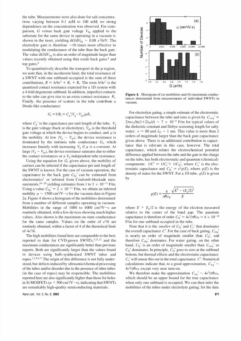
SWNTs. Figure 3 shows a grayscale plot of the current of
the device shown in Figure 2b as a function of both V sd and
V wg. The low conductance region corresponding to the band
gap of the tube is clearly seen, with p- and n-type
conductance observed at negative and positive V wg, respec-
tively. The low-conductance region is trapezoidal in shape,
with the boundaries given by a line with slope dV sd /dV wg =
1. The device conductance diminishes exponentially in the
subthreshold (gap) region as is seen in the inset to Figure
2b. The slope of the exponential falloff gives a device
parameter known as the subthreshold swing S ) - [d(logG)/ dV wg]-1, which is ∼80 mV/decade for this device. Other
devices give similar values.
Theoretically, the exponential falloff corresponds to
thermal activation of carriers in the semiconductor: G ∼
exp(- E b / kT ) where E b is the energy from the Fermi level to
the nearest of the conduction and valence bands. This barrier
height changes linearly with V wg: δ E b ) eRδV wg, where R
is a numerical constant that measures the effectiveness with
which the gate modulates the band energies. The theoretical
upper limit R ) 1 gives S ) 60 mV/decade. For the device
in Figure 2b (S ) 80 mV/decade), R ) 0.75; this is the
highest value reported to date for SWNT transistors. The
constant R can be used to infer the band gap of the tube of Figure 2b/Figure 3. From the measured width of the gap
∆V wg ∼ 0.45 V , we obtain E g ) eR∆V wg ∼ 0.33 eV. This is
in reasonable agreement with the expected value for a 3-nm
tube obtained from the relation E g ) 0.8 eV / d [nm].12
Note that the size of the gap between n- and p-behavior
decreases with increasing the diameter of the tube, as does
the on-state conductance in n-type region compared to the
p-region. This is evident from the traces of G vs V wg in Figure
2. The suppression of n-type transport in small diameter tubes
is consistent with previous measurements with back gated
samples, where n-type transport was observable only in
larger-diameter tubes5,13 or in tubes whose contacts have been
doped n-type.14-17 This results from the fact that, under
ambient conditions, Au contacts form p-type contacts to the
tube. Depletion barriers thus form at the contacts in n-type
operation, creating a large contact resistance to the tube. This
barrier is larger the larger the band gap of the tube. As a
result of these contact issues for n-type operation, we will
concentrate our analysis on p-type operation.
The conductance change in the linear p-region for the
device in Figure 2a is dG /dV wg ∼ 1 e2 / h / V . Measurements
from many other devices show similar behavior, with no
obvious correlation between dG /dV wg and the diameter of
Figure 2. Conductance G versus water gate voltage V wg for threetubes with lengths and diameters given by: (a) L ) 1 µm, d ) 1.1
nm, (b) L ) 1.4 µm, d ) 3 nm, and (c) L ) 2.2 µm, d ) 4.3 nmwide. Inset to (a): G versus the back gate voltage V bg for the samedevice measured in vacuum; the slope of linear regime is given bydashed line. Inset to (b): Logarithmic scale plot showing theexponential dependence of G on V wg for the same device.
Figure 3. Grayscale plot of current on a logarithmic scale versusV wg and V sd for the device of Figure 2b. The band gap region isgiven by the dark trapezoid at the center.
870 Nano Lett., Vol. 2, No. 8, 2002
8/3/2019 Tatler, Sep 2011
http://slidepdf.com/reader/full/tatler-sep-2011 3/4
the tube. Measurements were also done for salt concentra-
tions varying between 0.1 mM to 100 mM; no strong
dependence on the concentration was observed. For com-
parison, G versus back gate voltage V bg applied to the
substrate for the same device in operating in a vacuum is
shown in the inset, yielding dG /dV bg ∼ 0.08 e2 / h / V . The
electrolyte gate is therefore ∼10 times more effective in
modulating the conductance of the tube than the back gate.
The value dG /dV wg is also an order of magnitude larger than
values recently obtained using thin oxide back gates4
andtop gates.6
To quantitatively describe the transport in the p-region,
we note that, in the incoherent limit, the total resistance of
a SWNT with one subband occupied is the sum of three
contributions, R ) h/ 4e2 + Rc + Rt. The term h /4e2 is the
quantized contact resistance expected for a 1D system with
a 4-fold degenerate subband. In addition, imperfect contacts
to the tube can give rise to an extra contact resistance Rc.
Finally, the presence of scatters in the tube contribute a
Drude-like conductance:
where C g′ is the capacitance per unit length of the tube, V gis the gate voltage (back or electrolyte), V go is the threshold
gate voltage at which the device begins to conduct, and µ is
the mobility. At low |V g - V go|, the device resistance is
dominated by the intrinsic tube conductance Gt, which
increases linearly with increasing V g if µ is a constant. At
large |V g - V go|, the device resistance saturates due to either
the contact resistances or a V g-independent tube resistance.
Using the equation for Gt given above, the mobility of
carriers can be inferred if the capacitance per unit length of
the SWNT is known. For the case of vacuum operation, the
capacitance to the back gate C bg′ can be estimated from
electrostatics1 or inferred from Coulomb-blockade mea-surements,18-20 yielding estimates from 1 to 3 × 10-11 F/m.
Using a value C bg′ ) 2 × 10-11 F/m, we obtain an inferred
mobility µ ∼ 1500 cm2 /V-s for the vacuum data in Figure
2a. Figure 4 shows a histogram of the mobilities determined
from a number of different samples operating in vacuum.
Mobilities in the range of 1000 to 4000 cm2 /V-s are
routinely obtained, with a few devices showing much higher
values. Also shown is the maximum on-state conductance
for the same samples. Values on the order of e2 / h are
routinely obtained, within a factor of 4 of the theoretical limit
of 4e2 / h.
The high mobilities found here are comparable to the best
reported to date for CVD-grown SWNTs,3,21,22 and the
maximum conductances are significantly better than previous
reports. Both are significantly larger than the values found
in devices using bulk-synthesized SWNT tubes and
ropes.1,2,4,6,17 The origin of this difference is not fully under-
stood, but defects induced by ultrasonic/chemical processing
of the tubes and/or disorder due to the presence of other tubes
(in the case of ropes) may be responsible. The mobilities
reported here are also significantly higher than those for holes
in Si MOSFETs ( µ < 500 cm2 /V-s), indicating that SWNTs
are remarkably high-quality semiconducting materials.
For electrolyte gating, a simple estimate of the electrostatic
capacitance between the tube and ions is given by C ewg′ )
2π o /ln(1+2 λD / d ) ∼ 7 × 10⁻⁹ F/m for typical values of
the dielectric constant and Debye screening length for salty
water: ) 80 and λD ∼ 1 nm. This value is more than 2
orders of magnitude larger than the back gate capacitance
given above. There is an additional contribution to capaci-
tance that is relevant in this case, however. The total
capacitance, which relates the electrochemical potential
difference applied between the tube and the gate to the charge
on the tube, has both electrostatic and quantum (chemical)
components: 1/ C ′ ) 1/ C e′+ 1/ C Q′, where C e′ is the elec-
trostatic capacitance and C Q′ ) e2g( E ), where g( E ) is the
density of states for the SWNT. For a 1D tube, g( E ) is given
by
where E > E g /2 is the energy of the electron measured
relative to the center of the band gap. The quantum
capacitance is therefore of order C Q′ ) 4e2 / π pVF ) 4 × 10⁻¹⁰
F/m for one subband occupied in the tube.
Note that it is the smaller of C Q′ and C e′ that dominates
the overall capacitance C ′. For the case of back gating, C ebg′
is nearly an order of magnitude smaller than C Q′, and
therefore C ebg′ dominates. For water gating, on the other
hand, C Q′ is an order of magnitude smaller than C ewg′ so
C Q′ dominates. In principle, C Q′ goes to zero at the subband
bottom, but thermal effects and the electrostatic capacitance
C e′ will smear this out in the total capacitance C ′. Numerical
calculations indicate that, to a good approximation, C wg′ ∼
4e2 / π pVF except very near turn-on.
We therefore make the approximation C wg′ ∼ 4e2 / π pVF,
which should be an upper bound for the true capacitance
when only one subband is occupied. We can then infer the
mobilities of the tubes under electrolyte gating; for the data
Gt )1/ Rt ) C g′|V g-V go| µ /L
Figure 4. Histogram of (a) mobilities and (b) maximum conduc-tances determined from measurements of individual SWNTs invacuum.
g( E ) )4
π pVF
E 2
- ( E g /2)2
E
Nano Lett., Vol. 2, No. 8, 2002 871
8/3/2019 Tatler, Sep 2011
http://slidepdf.com/reader/full/tatler-sep-2011 4/4
in Figure 2a, this gives µ ∼ 1000 cm2 /V-s. This is in good
agreement with the mobility obtained for the same device
in vacuum, µ ) 1500 cm2
/V-s. This agreement implies that(a) the mobility of the tube is not dramatically affected by
the electrolyte, and (b) the elecrolyte tube capacitance is near
the quantum capacitance. These measurements illustrate that
water-gated nanotube FETs approach the ultimate limit where
the capacitance is governed by quantum effects and not
electrostatics.
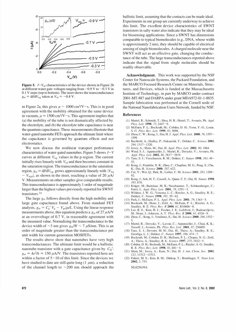
We now discuss the nonlinear transport performance
characteristics of water-gated nanotubes. Figure 5 shows I -V
curves at different V wg values in the p-region. The current
initially rises linearly with V sd and then becomes constant in
the saturation region. The transconductance in the saturation
region, gm ) d I /dV wg , grows approximately linearly with |V wg
- V wgo|, as shown in the inset, reaching a value of 20 µA/ V. Measurements on other samples give comparable results.
This transconductance is approximately 1 order of magnitude
larger than the highest values previously reported for SWNT
transistors.3,6
The large gm follows directly from the high mobility and
large gate capacitance found above. From standard FET
analysis, gm ) C g′|V g - V go| µ /L. Using the linear response
measurements above, this equation predicts a gm of 27 µA/V
at an overvoltage of 0.7 V, in reasonable agreement with
the measured value. Normalizing the transconductance to the
device width of ∼3 nm gives gm / W ∼ 7 µS/nm. This is an
order of magnitude greater than the transconductance per
unit width for current-generation MOSFETs.The results above show that nanotubes have very high
transconductances. The ultimate limit would be a ballistic
nanotube transistor with a gate capacitance given by C Q′:
gm ) 4e2 / h ) 150 µA/V. The transistors reported here are
within a factor of 5-10 of this limit. Since the devices we
have studied to date are still quite long (1 µm), a reduction
of the channel length to ∼200 nm should approach the
ballistic limit, assuming that the contacts can be made ideal.
Experiments in our group are currently underway to achieve
this limit. The excellent device characteristics of SWNT
transistors in salty water also indicate that they may be ideal
for biosensing applications. Since a SWNT has dimensions
comparable to typical biomolecules (e.g., DNA, whose width
is approximately 2 nm), they should be capable of electrical
sensing of single biomolecules. A charged molecule near the
SWNT will act as an effective gate, changing the conduc-
tance of the tube. The large transconductances reported aboveindicate that the signal from single molecules should be
readily observable.
Acknowledgment. This work was supported by the NSF
Center for Nanoscale Systems, the Packard Foundation, and
the MARCO Focused Research Center on Materials, Struc-
tures, and Devices, which is funded at the Massachusetts
Institute of Technology, in part by MARCO under contract
2001-MT-887 and DARPA under grant MDA972-01-1-0035.
Sample fabrication was performed at the Cornell node of
the National Nanofabrication Users Network, funded by NSF.
References
(1) Martel, R.; Schmidt, T.; Shea, H. R.; Hertel, T.; Avouris, Ph. Appl.Phys. Lett. 1998, 73, 2447-9.
(2) McEuen, P. L.; Bockrath, M.; Cobden, D. H.; Yoon, Y.-G.; Louie,S. G. Phys. ReV. Lett. 1999, 83, 5098.
(3) Zhou, C. W.; Kong, J.; Dai, H. J. Appl. Phys. Lett. 2000, 76 , 1597-
1599.(4) Bachtold, A.; Hadley, P.; Nakanishi, T.; Dekker, C. Science 2001,
294, 1317-1320.(5) Javey, A.; Shim, M.; Dai, H. Appl. Phys. Lett. 2002, 80, 1064.(6) Wind, S. J.; Appenzeller, J.; Martel, R.; Derycke, V.; Avouris, Ph.
Appl. Phys. Lett. 2002, 80, 3817-3819.(7) Tans, S. J.; Verschueren, R. M.; Dekker, C. Nature 1998, 393, 49-
52.(8) Kong, J.; Franklin, N. R.; Zhou, C.; Chapline, M. G.; Peng, S.; Cho,
K.; Dai, H. Science 2000, 287 , 622.(9) Cui, Y.; Wei, Q.; Park, H.; Lieber, C. M. Science 2001, 293, 1289-
92.(10) Kong, J.; Soh, H. T.; Cassell, A.; Quate, C. F.; Dai, H. Nature 1998,
395, 878.(11) Kruger, M.; Buitelaar, M. R.; Nussbaumer, T.; Schonenberger, C.;
Forro, L. Appl. Phys. Lett. 2001, 78, 1291-3.(12) Wildoer, J. W. G.; Venema, L. C.; Rinzler, A. G.; Smalley, R. E.;
Dekker, C. Nature 1998, 391, 59-62.(13) Park, J.; McEuen, P. L. Appl. Phys. Lett. 2001, 79, 1363-5.(14) Bockrath, M.; Hone, J.; Zettl, A.; McEuen, P. L.; Rinzler, A. G.;
Smalley, R. E. Phys. ReV. B 2000, 61, R10606-8.(15) Lee, R. S.; Kim, H. J.; Fischer, J. E.; Lefebvre, J.; Radosavljevic,
M.; Hone, J.; Johnson, A. T. Phys. ReV. B 2000, 61, 4526-9.(16) Zhou, C.; Kong, J.; Yenilmez, E.; Dai, H. Science 2000, 290, 1552-
5.(17) Martel, R.; Derycke, V.; Lavoie, C.; Appenzeller, J.; Chan, K. K.;
Tersoff, J.; Avouris, Ph. Phys. ReV. Lett. 2001, 87 , 256805.(18) Tans, S. J.; Devoret, M. H.; Dai, H.; Thess, A.; Smalley, R. E.;
Georliga, L. J.; Dekker, C. Nature 1997, 386 , 474-7.(19) Bockrath, M.; Cobden, D. H.; McEuen, P. L.; Chopra, N. G.; Zettl,
A.; Thess, A.; Smalley, R. E. Science 1997, 275, 1922-5.(20) Cobden, D. H.; Bockrath, M.; McEuen, P. L.; Rinzler, A. G.; Smalley,
R. E. Phys. ReV. Lett. 1998, 81, 681-4.(21) Shim, M.; Javey, A.; Kam, N.; Dai, H. J. Am. Chem. Soc. 2001,
123, 11512-11513.(22) Fuhrer, M. S.; Kim, B. M.; Durkop, T.; Brintlinger, T. Nano Lett .
2002, 2, 755.
NL025639A
Figure 5. I -V sd characteristics of the device shown in Figure 2bat different water gate voltages ranging from -0.9 V to -0.3 V in0.1 V steps (top to bottom). The inset shows the transconductancegm ) d I /dV wg taken at V sd ) -0.8 V.
872 Nano Lett., Vol. 2, No. 8, 2002