Embed Size (px)
Citation preview
1
Tantalum Carbide and Nitride Diffusion Barriers for Cu Metallisation
T. Laurilaa) , K. Zeng and J.K. KivilahtiLab. of Electronics Production Technology,P.O.Box 3000, FIN-02015 HUT, Finland
J. Molarius, T. Riekkinen and I.Suni VTT Microelectronics, P.O.Box 1101, FIN-02044 VTT, Finland
ABSTRACT
The reactions in the Si/TaC/Cu and Si/Ta2N/Cu metallisation systems were investigated
by x-ray diffraction, Rutherford backscattering, scanning electron microscope and the
transmission electron microscopy. The results were then combined with the assessed ternary Si-
Ta-C, Ta-C-Cu, Si-Ta-N and Ta-N-Cu phase diagrams. It was found that both barriers ultimately
failed due to diffusion of Cu through the barrier and accompanied formation of Cu3Si at
temperatures higher than 725 °C. However, in the TaC barriers the formation of amorphous TaOx
layer with significant amounts of C took place at the TaC/Cu interface already at 600 °C. Similar
behaviour at "low" temperatures was also noted in the Ta2N barriers.
Keywords: Phase diagrams; diffusion barriers; copper metallisation, tantalum carbide; tantalum
nitride
a) corresponding author, e-mail: [email protected]
2
1. INTRODUCTION
Interest in copper for conduction lines and structures has been wide, since it offers many
advantages over the currently used Al based materials. Unfortunately, the interaction between Si
and Cu is strong and detrimental to the electrical performance of Si even at temperatures below
200 °C[1-3]. Thus, it is necessary to implement a barrier layer between Si and Cu. Refractory
metals such as tantalum are frequently suggested to be used as barrier layers in Cu metallised
IC's. However, according to our investigations thin elemental Ta barrier layers may not posses
sufficient stability when in contact with Si and Cu[4]. In order to improve the performance of the
barrier layers it is essential to understand the underlying mechanisms leading to the failure. This
can be achieved by using a combined thermodynamic and kinetic approach. By utilising this
method it was found that the use of binary tantalum compounds like tantalum nitride and
tantalum carbide could improve the performance of the barrier layers. The phase relations in the
Si/TaC/Cu and Si/Ta2N/Cu metallisation systems are examined with the help of the calculated
ternary phase diagrams. The information extracted from these diagrams are coupled with the
experimental results obtained to reveal the mechanism(s) leading to the failure.
2. MATERIALS AND METHODS
The Cu, TaC and Ta2N films were sputtered onto cleaned and oxide-stripped (100)
oriented n-type Si substrates in a cluster sputtering tool. The base pressure before the deposition
was about 3×10⁻⁵ Pa. Both diffusion barriers were rf-magnetron sputtered, Ta2N in
argon/nitrogen gas-mixture from the elemental target whereas TaC was obtained from the
3
compound target in argon atmosphere. Barrier thicknesses were about 10, 50 and 100 nm for
Ta2N and 7, 35, and 70 nm for TaC, as determined with RBS. The copper films (100 or 400 nm)
were subsequently sputtered onto Ta2N and TaC films from the dc-magnetron target without
breaking the vacuum. The samples were then annealed in the vacuum of about 10-4 Pa at
temperatures from 500 to 800 °C for 30 min. The reactions in the metallisation schemes were
investigated by the sheet resistance measurements, grazing incidence x-ray diffraction (XRD),
Rutherford backscattering spectroscopy (RBS), scanning electron microscope (SEM) and the
transmission electron microscopy (TEM). The results of the experimental investigations were
compared with the assessed phase diagrams. Ternary Si-Ta-C, Ta-C-Cu, Si-Ta-N and Ta-N-Cu
phase diagrams were calculated from the assessed binary thermodynamic data [5-10] and
compared with the experimental results obtained.
3. RESULTS AND DISCUSSION
The sheet resistance measurements vs. temperature of the Si/TaC(70nm)/Cu(400nm)
samples showed an abrupt rise in the sheet resistance at 775 °C indicating that a reaction had
occurred. The 7 nm and 35 nm TaC layers were stable up to 550 °C and 650 °C, respectively.
The rise in the sheet resistance was accompanied with the loss of shiny copper-like appearance
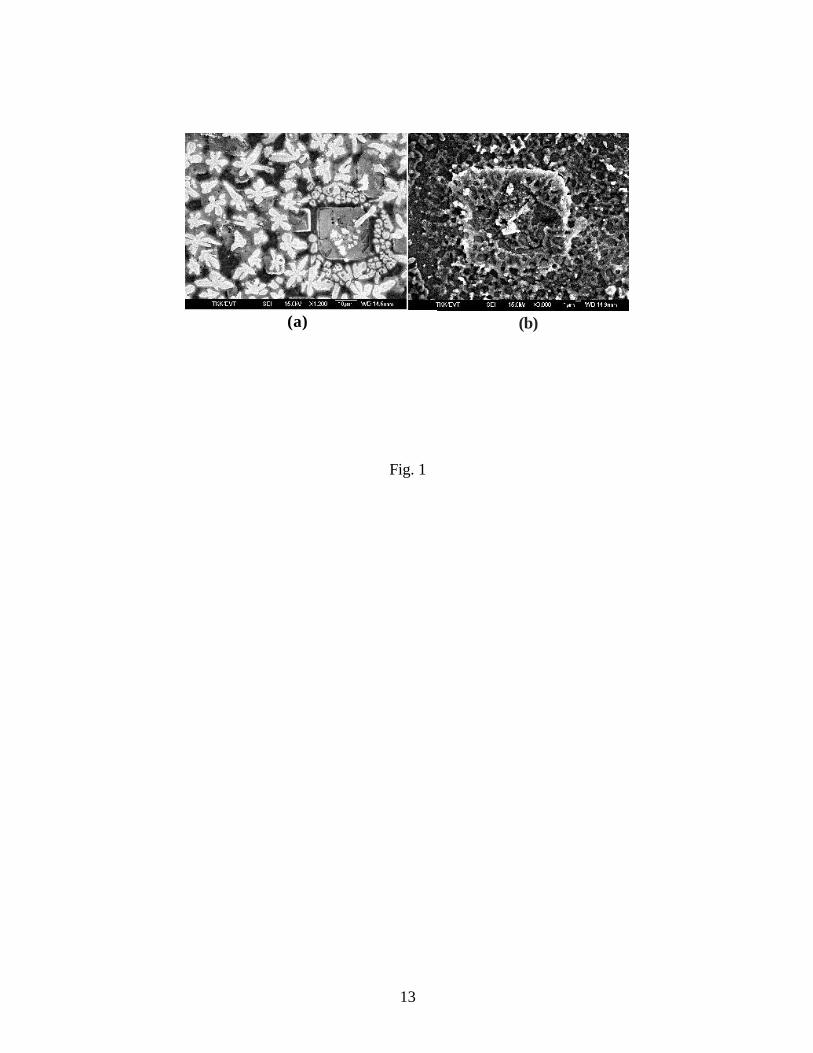
of the sample surface, regardless of the thickness. The SEM micrograph of the surface of the 70
nm TaC sample annealed at 800 °C is shown in Fig. 1(a). Large "squares" have formed on the
surface (about 20-30 µm in diameter). These "squares" are surrounded by a "flowery" patterned
structure, which seems to consist of one phase embedded into another.
4
The sheet resistance measurements of the Si/Ta2N(100nm)/Cu(400nm) showed an abrupt
rise in the sheet resistance at 775 °C and the samples with 10 and 50 nm Ta2N layers were stable
up to 625 °C and 675 °C, respectively. The surfaces of the Ta2N samples maintained their shiny
copper-like appearence up to 750 °C (100 nm), 650 °C (50 nm) and 600 °C (10 nm). The
structure formed on the surface after reaction(s) was very similar to that observed in the TaC
films. The SEM micrograph of the surface structure of the sample with 100 nm Ta2N barrier
annealed at 775 °C is shown in Fig. 1(b).
The RBS analyses of the as deposited TaC samples showed sharp edges of the elements
in the spectra indicating that the layers were clearly discrete at this stage. The spectra from the
annealed samples with the 70 nm thick TaC layers showed that some reaction(s) had taken place
already at 600 °C (Fig.2). As can be seen, the spectrum has been graded and tantalum has moved
towards the surface. This indicates that the TaC layer has decomposed, which is not expected
based on the high thermal stability of TaC compound. From the spectra taken at higher
temperatures, it was very difficult to obtain more information about the reactions taking place, as
the surface of the samples did not stay planar (see Figs. 1 (a) and (b)) the interpretation of RBS
spectrum was not unambigious.
The RBS analyses of the as deposited Ta2N samples showed also clearly discrete layers
before the annealings. The layer thicknessess were about 10, 50 and 100 nm. The spectra from
the sample with 100 nm thick Ta2N layers showed that some reaction(s) took place at 650 °C
(Fig. 3). The temperature was again unexpectedly low as with the TaC layers. At higher
temperatures the spectra further degraded and no additional information could be obtained.
5
Hence, the RBS results showed that something unforeseen took place at low temperatures in both
metallisation systems.
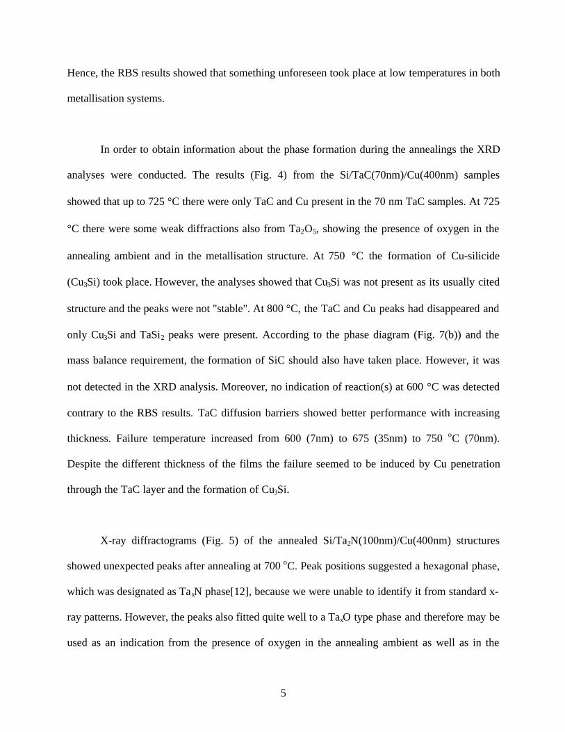
In order to obtain information about the phase formation during the annealings the XRD
analyses were conducted. The results (Fig. 4) from the Si/TaC(70nm)/Cu(400nm) samples
showed that up to 725 °C there were only TaC and Cu present in the 70 nm TaC samples. At 725
°C there were some weak diffractions also from Ta2O5, showing the presence of oxygen in the
annealing ambient and in the metallisation structure. At 750 °C the formation of Cu-silicide
(Cu3Si) took place. However, the analyses showed that Cu3Si was not present as its usually cited
structure and the peaks were not "stable". At 800 °C, the TaC and Cu peaks had disappeared and
only Cu3Si and TaSi2 peaks were present. According to the phase diagram (Fig. 7(b)) and the
mass balance requirement, the formation of SiC should also have taken place. However, it was
not detected in the XRD analysis. Moreover, no indication of reaction(s) at 600 °C was detected
contrary to the RBS results. TaC diffusion barriers showed better performance with increasing
thickness. Failure temperature increased from 600 (7nm) to 675 (35nm) to 750 oC (70nm).
Despite the different thickness of the films the failure seemed to be induced by Cu penetration
through the TaC layer and the formation of Cu3Si.
X-ray diffractograms (Fig. 5) of the annealed Si/Ta2N(100nm)/Cu(400nm) structures
showed unexpected peaks after annealing at 700 oC. Peak positions suggested a hexagonal phase,
which was designated as TaxN phase[12], because we were unable to identify it from standard x-
ray patterns. However, the peaks also fitted quite well to a TaxO type phase and therefore may be
used as an indication from the presence of oxygen in the annealing ambient as well as in the
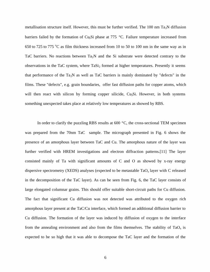
6
metallisation structure itself. However, this must be further verified. The 100 nm Ta2N diffusion
barriers failed by the formation of Cu3Si phase at 775 °C. Failure temperature increased from
650 to 725 to 775 oC as film thickness increased from 10 to 50 to 100 nm in the same way as in
TaC barriers. No reactions between Ta2N and the Si substrate were detected contrary to the
observations in the TaC system, where TaSi2 formed at higher temperatures. Presently it seems
that performance of the Ta2N as well as TaC barriers is mainly dominated by "defects" in the
films. These "defects", e.g. grain boundaries, offer fast diffusion paths for copper atoms, which
will then react with silicon by forming copper silicide, Cu3Si. However, in both systems
something unexpected takes place at relatively low temperatures as showed by RBS.
In order to clarify the puzzling RBS results at 600 °C, the cross-sectional TEM specimen
was prepared from the 70nm TaC sample. The micrograph presented in Fig. 6 shows the
presence of an amorphous layer between TaC and Cu. The amorphous nature of the layer was
further verified with HREM investigations and electron diffraction patterns.[11] The layer
consisted mainly of Ta with significant amounts of C and O as showed by x-ray energy
dispersive spectrometry (XEDS) analyses (expected to be metastable TaOx layer with C released
in the decomposition of the TaC layer). As can be seen from Fig. 6, the TaC layer consists of
large elongated columnar grains. This should offer suitable short-circuit paths for Cu diffusion.
The fact that significant Cu diffusion was not detected was attributed to the oxygen rich
amorphous layer present at the TaC/Cu interface, which formed an additional diffusion barrier to
Cu diffusion. The formation of the layer was induced by diffusion of oxygen to the interface
from the annealing environment and also from the films themselves. The stability of TaOx is
expected to be so high that it was able to decompose the TaC layer and the formation of the

7
observed amorphous interlayer took place. However, this must be verified with detailed
thermodynamic description of the Ta-C-O system, which is currently under construction. The
carbon found in the amorphous layer is a result of the dissociation of TaC layer at the TaC/Cu
interface. Only after suitable high temperature is reached, the amorphous layer is partly or
completely crystallised and the diffusion of Cu will proceed. The observation of the amorphous
interlayer formation between TaC and Cu gives some indication why the RBS spectrum has
degraded already at 600 °C. From the sample annealed at 750 °C (Fig. 7) one could observe Si-
O, TaOx along with the very large Cu3Si protrusions. This shows that at 750 °C Cu atoms have
been able to diffuse through the partly crystallised amorphous layer to the Si/TaC interface and
the formation of Cu3Si has taken place. However, no crystalline tantalum silicides were detected
and there was still large amount of the amorphous oxide rich layer present. At still higher
temperatures (800 °C) XTEM investigations showed the formation of TaSi2 and SiC, which was
expected based on the thermodynamic evaluation of the metallisation system. Similar behaviour
is also anticipated to take place in the Ta2N films at 650 °C, since it seems that the annealing
ambient as well as the films contained some oxygen also in Ta2N case (see the XRD results) and
the RBS results showed similar behaviour in comparision to the TaC films. Unfortunately
detailed TEM results are not yet available.
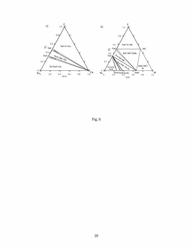
The phase relationships in the Si-Ta-C, Si-Ta-N, and in the Ta-C-Cu, Ta-N-Cu phase
diagrams are very similar. Figure 8 (a) shows the evaluated isothermal section of the ternary Ta-
C-Cu phase diagram. It can be seen that Cu is in equilibrium with both TaC and Ta2C. Thus, the
reactions at the interface Cu/TaC do not have driving force because the interface is already in
local thermodynamic equilibrium. Nevertheless, the driving force for copper diffusion through
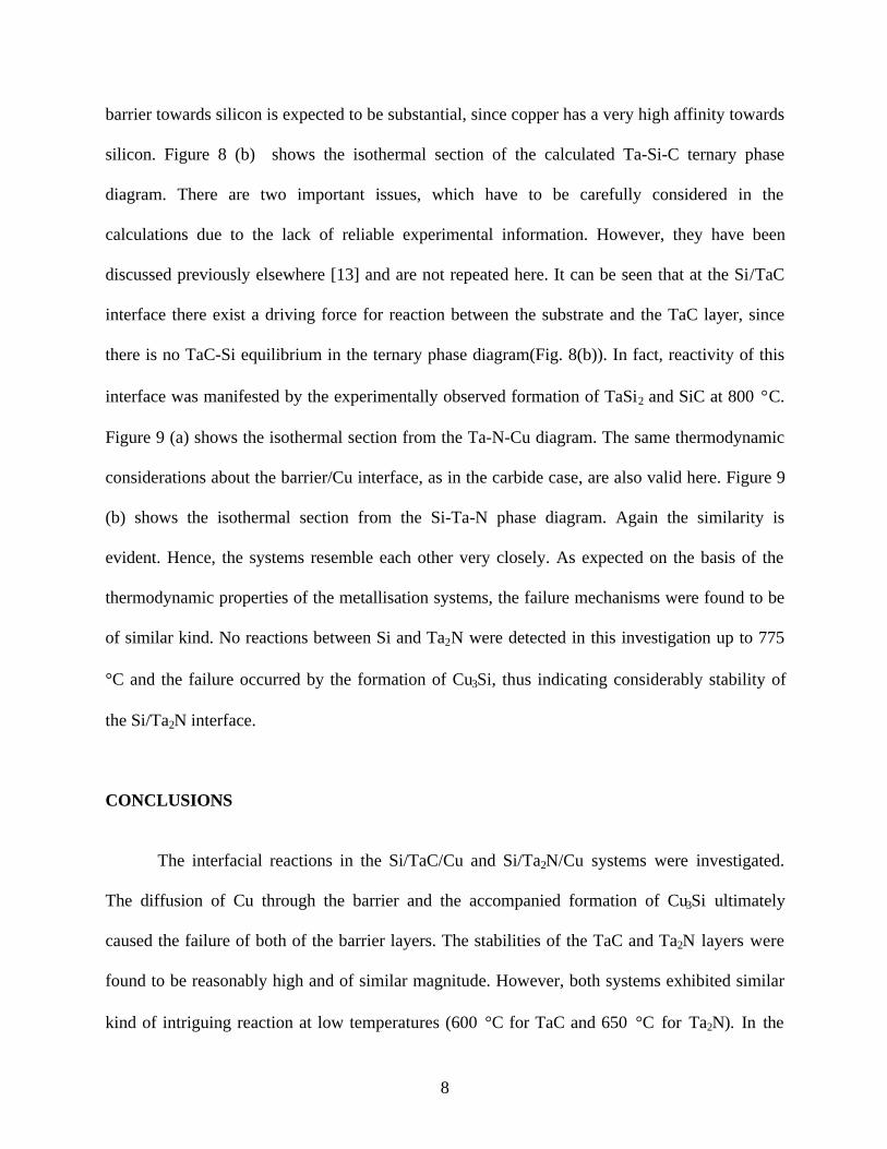
8
barrier towards silicon is expected to be substantial, since copper has a very high affinity towards
silicon. Figure 8 (b) shows the isothermal section of the calculated Ta-Si-C ternary phase
diagram. There are two important issues, which have to be carefully considered in the
calculations due to the lack of reliable experimental information. However, they have been
discussed previously elsewhere [13] and are not repeated here. It can be seen that at the Si/TaC
interface there exist a driving force for reaction between the substrate and the TaC layer, since
there is no TaC-Si equilibrium in the ternary phase diagram(Fig. 8(b)). In fact, reactivity of this
interface was manifested by the experimentally observed formation of TaSi2 and SiC at 800 °C.
Figure 9 (a) shows the isothermal section from the Ta-N-Cu diagram. The same thermodynamic
considerations about the barrier/Cu interface, as in the carbide case, are also valid here. Figure 9
(b) shows the isothermal section from the Si-Ta-N phase diagram. Again the similarity is
evident. Hence, the systems resemble each other very closely. As expected on the basis of the
thermodynamic properties of the metallisation systems, the failure mechanisms were found to be
of similar kind. No reactions between Si and Ta2N were detected in this investigation up to 775
°C and the failure occurred by the formation of Cu3Si, thus indicating considerably stability of
the Si/Ta2N interface.
CONCLUSIONS
The interfacial reactions in the Si/TaC/Cu and Si/Ta2N/Cu systems were investigated.
The diffusion of Cu through the barrier and the accompanied formation of Cu3Si ultimately
caused the failure of both of the barrier layers. The stabilities of the TaC and Ta2N layers were
found to be reasonably high and of similar magnitude. However, both systems exhibited similar
kind of intriguing reaction at low temperatures (600 °C for TaC and 650 °C for Ta2N). In the

9
TaC case the reaction was found to be an amorphous TaOx layer formation at the TaC/Cu
interface. Formation of similar kind of layer is also expected to take place in the Si/Ta2N/Cu
system. The observed similarities in the behaviour of the carbide and nitride films can be
understood with the help of the corresponding evaluated Si-Ta-C, Si-Ta-N, Ta-C-Cu and Ta-N-
Cu ternary phase diagrams, which show almost identical phase relationships.
ACKNOWLEDGEMENTS
Authors greatly acknowledge J. Saarilahti and A. Nurmela from the VTT Microelectronics for
help in the RBS analyses. The work was financially supported by the Academy of Finland.
10
References:
[1] A.A. Istratov and E.R. Weber, Electrical Properties and Recombination Activity of
Copper, Nickel and Cobolt in Silicon, Appl. Phys. A, 66, (1998) 123-136.
[2] S.P. Murarka, Advanced Materials for Future Interconnections of the Future Need
and Strategy, Microelectronic Engineering, 37/38, (1997) 29-37.
[3] C-A. Chang, Formation of Copper Silicides from Cu(100)/Si(100) and
Cu(111)/Si(111) Structures, J. Appl. Phys. 67, (1990), 566-569.
[4] T.Laurila, K. Zeng, J.K. Kivilahti, J. Molarius and I. Suni, Failure Mechanism of Ta
Diffusion Barrier Between Cu and Si, J. Appl. Phys., 88, (2000) 3377-3384.
[5] J. Lacaze and B. Sundman, An Assessment of the Fe-C-Si System, Metall. Trans. A, 22,
(1991), 2211-2223.
[6] K. Frisk and A. F. Guillermet, Gibbs Energy Coupling of the Phase Diagram and
Thermochemistry in the Tantalum-Carbon System , J. Alloys Compd., 238, (1996),167-178.
[7] L. Chandra Sekaran, Cu-Fe-P-C, Report , Data in Thermo-Calc, (1987).
[8] K. Frisk, A Thermodynamic Evaluation of the Fe-Cu-C-N System, Report IM-2929,
Swedish Institute for Metals Research, Stockholm.
[9] M. Hillert, S. Jonsson, and B. Sundman, Thermodynamic Calculation of the Si-N-O
System, Z. Metallkde., 83, (1992), 648-654.
[10] K. Frisk, Analysis of the Phase Diagram and Thermochemistry in the Ta-N and the Ta-C-N
Systems, J. Alloys Compd., 278, (1998), 216-226.
[11] T.Laurila, K. Zeng, J.K. Kivilahti, J. Molarius and I. Suni, TaC as a Diffusion Barrier
Between Cu and Si, to be submitted.
11
[12] J. Molarius, T. Riekkinen, I. Suni, T. Laurila, K.Zeng and J.K. Kivilahti, Reactively
Sputtered Ta2N and TaN Diffusion Barriers for Copper Metallization, Advanced
Metallization Conference 2000 (AMC), San Diego, CA, 3-5 Oct., (2000), 137-138.
[13] T.Laurila, K. Zeng, J.K. Kivilahti, J. Molarius and I. Suni, Reliability of Tantalum Based
Diffusion Barriers between Copper and Silicon, 2000 MRS Spring Meeting (Materials
Research Society), San Francisco CA, 24-28 April, v612, (2000), 97.
12
FIGURE CAPTIONS
FIG.1. (a) SEM micrograph from the surface of the Si/TaC(70nm)/Cu(400nm) sample annealed
at 800 °C for 30 min and (b) SEM micrograph from the surface of the Si/Ta2N(100nm)/
Cu(400nm) sample annealed at 775 °C for 30 min.
FIG.2. RBS spectra (2.0 MeV 4 He+, θ = 170 °) from the Si/TaC(70nm)/Cu(400nm) samples
annealed at different temperatures for 30 min. Vertical arrows represent surface scattering
energies.
FIG.3. RBS spectra (2.0 MeV 4 He+, θ = 170 °) from the Si/Ta2N(100nm)/Cu(400nm) samples
annealed at different temperatures for 30 min. Vertical arrows represent surface scattering
energies.
FIG.4. XRD spectra from the Si/TaC(70nm)/Cu(400nm) samples annealed at different
temperatures.
FIG. 5. XRD spectra from the Si/Ta2N(100nm)/Cu(400nm) samples annealed at different
temperatures.
FIG.6. Bright field cross-sectional TEM micrograph from the Si/TaC(70nm)/Cu(400nm) sample
annealed at 600 °C for 30 min.
FIG.7. Bright field cross-sectional TEM micrograph from the Si/TaC(70nm)/Cu(400nm) sample
annealed at 750 °C for 30 min. Original surface is on the top of the figure.
FIG.8. (a) Isothermal section at 700 °C from the ternary Ta-C-Cu phase diagram (b) isothermal
section at 700 °C from the ternary Si-Ta-C phase diagram.
FIG.9. (a) Isothermal section at 700 °C from the ternary Ta-N-Cu phase diagram, (b) isothermal
section at 700 °C from the ternary Si-Ta-N phase diagram.
13
(a) (b)
Fig. 1
14
0
5000
10000
15000
20000
25000
0 100 200 300 400 500
0.5 1.0 1.5 2.0E (MeV)
Si Cu Ta
Channel number
RB
S yi
eld
(cou
nts/
chan
nel)
600 oC600 oC
725 oC725 oC
Fig. 2
15
0
5000
10000
15000
20000
25000
0 100 200 300 400 500
No annealing
650 oC
650 oC
0.5 1.0 1.5 2.0E (MeV)
Si Cu Ta
Channel number
RB
S yi
eld
(cou
nts/
chan
nel)
Fig. 3
16
0
50
100
150
200
250
20 30 40 50 60
l
n
v
TaCCu
Cu3Si
ur
Ta2O5
TaSi2
0
50
100
150
200
250
20 30 40 50 60
0
50
100
150
200
250
20 30 40 50 60
0
50
100
150
200
250
20 30 40 50 60
l
n
v
u
r
l l
l
n
n
ln
l
n
lul
n
v
l
r
r
r
r
vv
r
r
r r
600 oC
725 oC
750 oC
800 oC
2-Theta
Arb
itrar
y un
its
Fig. 4
17
0
100
200
300
400
500
20 30 40 50 60
0
100
200
300
400
500
20 30 40 50 60
0
100
200
300
400
500
20 30 40 50 60
vu
ln
CuTa2NTaxNCu3Si
600 oC
650 oC
775 oC
lnu
v
ln
ln n
ulu
u
ln
u
u
vv
l
2-Theta
Arb
itrar
y un
its
Fig. 5
18
TaC50 nm
a-Ta[O,C]
Cu
Fig. 6

19
Cu3Si
Cu3Si
Si-OCu
Cu
Si-O
Si-O
Si-O
SiTa[C]
300 nm
CuTa[O]
Fig. 7
20
C
Ta Cu0 0.2 0.4 0.6 0.8 1.0
x(Cu)
x(C)
0
0.2
0.4
0.6
0.8
1.0
TaC
Ta2C
TaC+C+Cu
Ta+Ta2C+Cu
Ta2C+TaC +CuTa2C+Cu
TaC+Cu
C
Ta Si
x(Si)
x(C)
0 0.2 0.4 0.6 0.8
0.8
1.0
1.0
0
0.2
0.4
0.6
TaC
Ta2C
SiC
Ta3Si Ta2Si Ta5Si3 TaSi2
TaC+C+SiC
TaC+SiC+TaSi2
TaSi2+SiC+ Si
Ta+Ta2C+ Ta3Si
Ta2C+TaC+TaSi
2Ta2C+TaSi
2+Ta5Si3
a) b)
Fig. 8

21
x(Cu)Ta Cu
N
x(N)
0
0
0.2
0.2
0.4
0.4
0.6
0.6
0.8
0.8
1.0
1.0
TaN
Ta2N{Ta2N+Cu
Ta2 N+TaN+Cu
TaN+N+ Cu
Ta+Ta2N+ Cu
0 0.2 0.4 0.6 0.8 1.0Tax(Si)
Si0
0.2
0.4
0.6
0.8
1.0N
x(N)
Si3N4
TaN
Ta2N
TaSi2Ta 5Si3Ta2Si
Ta3Si
TaN+N+Si3N4
TaN+Si3N4+TaSi2
TaSi2+Si3N4+Si Ta5Si3+
TaN+TaSi2
TaN+Ta2Si+Ta2NTa
2N+T
a3Si
Ta2N+Ta+Ta 3Si
a) b)
Fig. 9


![Engineering Ceramics: Carbide and Nitride Ceramicsweb.geni-pco.com/pacrim11/download/program/THJ3.pdf · Engineering Ceramics: Carbide and Nitride Ceramics [ThJ3] Mechanical Properties](https://img.pdfslide.us/doc/110x75/5f0dbcde7e708231d43bd689/engineering-ceramics-carbide-and-nitride-engineering-ceramics-carbide-and-nitride.jpg)