Embed Size (px)
Citation preview

303
Higher Secondary Second Year
PHYSICS
PRACTICAL
XII-Physics_Vol-1) PRACTICAL.indd 303 04-03-2019 11:06:33

304
LIST OF EXPERIMENTS
1. Determination of the specific resistance of the material of the given coil using metre bridge.
2. Determination of the value of the horizontal component of the Earth’s magnetic field using tangent galvanometer.
3. Determination of the magnetic field at a point on the axis of a circular coil.
4. Determination of the refractive index of the material of the prism by finding angle of prism and angle of minimum deviation using spectrometer.
5. Determination of the wavelength of a composite light by normal incidence method using diffraction grating and spectrometer (The number of lines per metre length of the grating is given).
6. Investigation of the voltage-current (V-I) characteristics of PN junction diode.
7. Investigation of the voltage-current (V-I) characteristics of Zener diode.
8. Investigation of the static characteristics of a NPN Junction transistor in common emitter configuration.
9. Verification of the truth table of the basic logic gates using integrated circuits.
10. Verification of De Morgan’s theorems using integrated circuits.
XII-Physics_Vol-1) PRACTICAL.indd 304 04-03-2019 11:06:33
305
1. SPECIFIC RESISTANCE OF THE MATERIAL OF THE COIL USING METRE BRIDGE
AIM To determine the specific resistance of the material of the given coil using metre bridge.
APPARATUS REQUIRED Meter bridge, galvanometer, key, resistance box, connecting wires, Lechlanche cell, jockey and high resistance.
FORMULA ρ π=X rL
2
(Ωm)
where, X → Resistance of the given coil (Ω)
R → Known resistance (Ω)
L → Length of the coil (m)
r → Radius of the wire (m)
CIRCUIT DIAGRAM
0 10 20 30 40 50 60 70 80 90 100
(
G2G1
lJA B
Lechlanche cell K
RX
)
G
HR
+ –
D
(100 - l)
PROCEDURE
• A resistance box R is connected in the left gap and the unknown resistance X in the right gap.
• A Lechlanche cell is connected across the wire of length 1 m through a key.
• A sensitive galvanometer G is connected between the central strip and the jockey through a high resistance (HR).
• With a suitable resistance included in the resistance box, the circuit is switched on.
• To check the circuit connections, the jockey is pressed near one end of the wire, say A. The galvanometer will show deflection in one direction. When the jockey is pressed near the other end of the wire B, the galvanometer will show deflection in the opposite directions. This ensures that the circuit connections are correct.
XII-Physics_Vol-1) PRACTICAL.indd 305 04-03-2019 11:06:34

306
• By moving the jockey over the wire, the point on the wire at which the galvanometer shows null deflection i.e., balancing point J is found.
• The balancing length AJ l= is noted.
• The unknown resistance X1 is found using the formula XR l
l1
100=
−( ).
• The experiment is repeated for different values of R.
• The same procedure is repeated after interchanging R and X.
• The unknown resistance X2 is found using the formula X Rll2
100=
−( ).
• The experiment is repeated for same values of R as before.
• The resistance of the given coil is found from the mean value of X1 and X2.
• The radius of the wire r is found using screw gauge.
• The length of the coil L is measured using meter scale.
• From the values of X, r and L, the specific resistance of the material of the wire is determined.
OBSERVATION
length of the coil L = ____________________________________ cm.
Table 1 To find the resistance of the given coil
S.No.Resistance
R (Ω)
Before interchanging After interchanging Mean
X X X=
+1 2
2
(Ω)
Balancing length l
(cm)X
R ll1
100=
−( )(Ω)
Balancing length l
(cm)X Rl
l2
100=
−( )(Ω)
1
2
3
Mean resistance, X = -----------Ω
XII-Physics_Vol-1) PRACTICAL.indd 306 04-03-2019 11:06:38
307
Table 2 To find the radius of the wire Zero error = Zero correction = LC = 0.01 mm
Sl.No.PSR(mm)
HSC(div.)
Total Reading= PSR + (HSC × LC)
(mm)
Corrected Reading = TR ± ZC
(mm)123456
Mean diameter 2r = . . . . . . . . . . . cm Radius of the wire r = . . . . . . . . . . . cm r = . . . . . . . . . . . m
CALCULATION
(i) ρ π=X rL
2
=
RESULT
The specific resistance of the material of the given coil = _____________________(Ωm)
Note:
i) To check the circuit connections:
The meter bridge wire is touched near one end (say, end A) with jockey, galvanometer shows a deflection in any one direction. Now the other end (say, end B) is touched. If the galvanometer shows a deflection in the opposite direction, then the circuit connections are correct.
ii) The usage of high resistance (HR):
The galvanometer is a very sensitive device. If any high current flows through the galvanom-eter, its coil gets damaged. Therefore in order to protect the galvanometer, a high resistance (HR) is used. When HR is connected in series with the galvanometer, the current through it is reduced so that the galvanometer is protected. But the balancing length is not accurate.
iii) To find the accurate balancing length:
The HR is first included in the circuit (that is, the plug key in HR is removed), the approx-imate balancing length is found. Now HR is excluded in the circuit (that is, the plug key in HR is closed), then the accurate balancing length is found.
XII-Physics_Vol-1) PRACTICAL.indd 307 04-03-2019 11:06:38
308
2. HORIZONTAL COMPONENT OF EARTH’S MAGNETIC FIELD USING TANGENT GALVANOMETER
AIM To determine the horizontal component of the Earth’s magnetic field using tangent galvanometer.
APPARATUS REQUIRED Tangent galvanometer (TG), commutator, battery, rheostat, ammeter, key and connecting wires.
FORMULA BnkrH =
µ0
2 (Tesla)
k I=
tanθ (A)
where, BH → Horizontal component of the Earth’s magnetic field (T)
µ0 → Permeability of free space (4π × 10−7 H m−1)
n → Number of turns of TG in the circuit (No unit)
k → Reduction factor of TG (A)
r → Radius of the coil (m)
CIRCUIT DIAGRAMClrcular coil
Compass box
Leveling screw
Pointer
Terminals
Figure (a) Tangent Galvanometer Figure (b) Number of turns
Rh
+
+
–
–
k
TG
Bt
A
( )C
(c) Circuit diagram
XII-Physics_Vol-1) PRACTICAL.indd 308 04-03-2019 11:06:39
309
PROCEDURE
• The preliminary adjustments are carried out as follows.
a. The leveling screws at the base of TG are adjusted so that the circular turn table is horizontal and the plane of the circular coil is vertical.
b. The circular coil is rotated so that its plane is in the magnetic meridian i.e., along the north-south direction.
c. The compass box alone is rotated till the aluminium pointer reads 0 0° − °.
• The connections are made as shown in Figure (c).
• The number of turns n is selected and the circuit is switched on.
• The range of current through TG is chosen in such a way that the deflection of the aluminium pointer lies between 30 60° − °.
• A suitable current is allowed to pass through the circuit, the deflections θ1 and θ2 are noted from two ends of the aluminium pointer.
• Now the direction of current is reversed using commutator C, the deflections θ3 and θ4 in the opposite direction are noted.
• The mean value θ of θ1, θ2, θ3 and θ4 is calculated and tabulated.
• The reduction factor k is calculated for each case and it is found that k is a constant.
• The experiment is repeated for various values of current and the readings are noted and tabulated.
• The radius of the circular coil is found by measuring the circumference of the coil using a thread around the coil.
• From the values of r, n and k, the horizontal component of Earth’s magnetic field is determined.
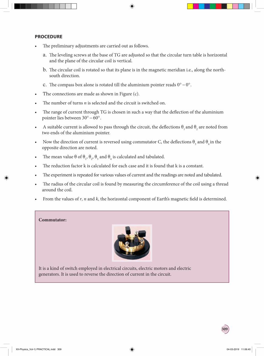
Commutator:
It is a kind of switch employed in electrical circuits, electric motors and electric generators. It is used to reverse the direction of current in the circuit.
XII-Physics_Vol-1) PRACTICAL.indd 309 04-03-2019 11:06:40
310
OBSERVATION
Number of turns of the coil n =
Circumference of the coil (2πr) =
Radius of the coil r =
S.No Current I
(A)
Deflection in TG (degree) Mean θ
(degree)k I=
tanθθ1 θ2 θ3 θ4
1234
Mean
CALCULATION
BnkrH =
µ0
2=
RESULT
The horizontal component of Earth’s magnetic field is found to be ________
Note:
i) The magnetic materials and magnets present in the vicinity of TG should be removed.
ii) The readings from the ends of the aluminium pointer should be taken without parallax error.
iii) The deflections of TG is restricted between 30° and 60°. It is because, the TG is most sensi tive for deflection around 45° and is least sensitive around 0° and 90°. We know that
I = k tan θ
or dI =k sec2 θ dθ
ddI Iθ θ=
sin22
For given current, sensitivity ddIθ maximum for sin 2θ = 1 or θ = 45°
XII-Physics_Vol-1) PRACTICAL.indd 310 04-03-2019 11:06:41
311
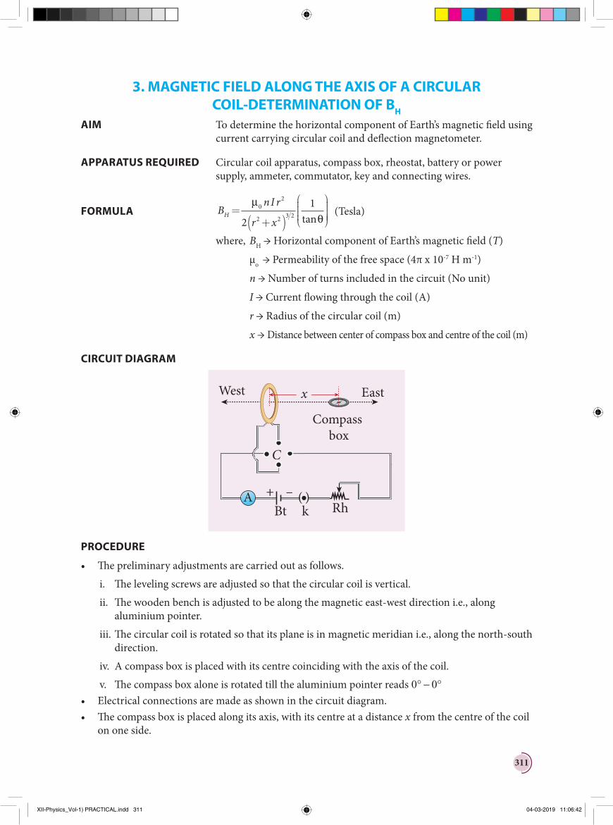
3. MAGNETIC FIELD ALONG THE AXIS OF A CIRCULAR COIL-DETERMINATION OF BH
AIM To determine the horizontal component of Earth’s magnetic field using current carrying circular coil and deflection magnetometer.
APPARATUS REQUIRED Circular coil apparatus, compass box, rheostat, battery or power supply, ammeter, commutator, key and connecting wires.
FORMULA BnI r
r xH=
+( )
µθ
02
2 2 3 22
1tan
(Tesla)
where, BH → Horizontal component of Earth’s magnetic field (T)
µo → Permeability of the free space (4π x 10-7 H m-1)
n → Number of turns included in the circuit (No unit)
I → Current flowing through the coil (A)
r → Radius of the circular coil (m)
x → Distance between center of compass box and centre of the coil (m)
CIRCUIT DIAGRAM
Rh+ –
kBtA ( )
Compass box
West East
C
x
PROCEDURE
• The preliminary adjustments are carried out as follows.
i. The leveling screws are adjusted so that the circular coil is vertical.
ii. The wooden bench is adjusted to be along the magnetic east-west direction i.e., along aluminium pointer.
iii. The circular coil is rotated so that its plane is in magnetic meridian i.e., along the north-south direction.
iv. A compass box is placed with its centre coinciding with the axis of the coil.
v. The compass box alone is rotated till the aluminium pointer reads 0 0° − °• Electrical connections are made as shown in the circuit diagram.• The compass box is placed along its axis, with its centre at a distance x from the centre of the coil
on one side.
XII-Physics_Vol-1) PRACTICAL.indd 311 04-03-2019 11:06:42

312
• A suitable current (1A) is passed through the coil by adjusting rheostat so that the deflection of the aluminium pointer lies between 30o and 60o.
• The value of the current I is noted from ammeter.
• Two readings θ1 and θ2 corresponding to two ends of the pointer are noted.
• Now the direction of the current is reversed using commutator, two more readings θ3 and θ4 are noted.
• Now the compass box is taken to the other side and is kept at the same distance x.
• Four more readings θ5, θ6, θ7 and θ8 are taken as done before.
• These eight readings and their average value are tabulated.
• The experiment is repeated for another value of current, say 1.5 A by keeping the compass box at the same distance x.
• The radius of the circular coil is found by measuring the circumference of the coil using a thread around the coil.
• The number of turns n of the coil is noted.
• From the values of n, r, x and I/tanθ, the horizontal component of Earth’s magnetic field is now found using the formula.
OBSERVATION
Number of turns in the coil n=
Circumference of the coil (2πr) =
Radius of the coil r =
To find horizontal component of the Earth’s magnetic field
S.No
Distance
x
(cm)
Current
I
(A)
Deflection for eastern side
Deflection for western side
Mean θI
tanθθ1 θ2 θ3 θ4 θ5 θ6 θ7 θ8
Mean
CALCULATION
BnI r
r xH=
+( )
µθ
02
2 2 3 22
1tan
=
RESULT
Horizontal component of the Earth’s magnetic field at a place = _________T
XII-Physics_Vol-1) PRACTICAL.indd 312 04-03-2019 11:06:42
313
4. REFRACTIVE INDEX OF THE MATERIAL OF THE PRISMAIM To determine the refractive index of the material of a prism using
spectrometer.
APPARATUS REQUIRED Spectrometer, prism, prism clamp, sodium vapour lamp, spirit level.
FORMULA µ=
+
sin
sin
A D
A2
2
(No unit)
where, μ → Refractive index of the material of the prism (No unit)
A → Angle of the prism (degree)
D → Angle of minimum deviation (degree)
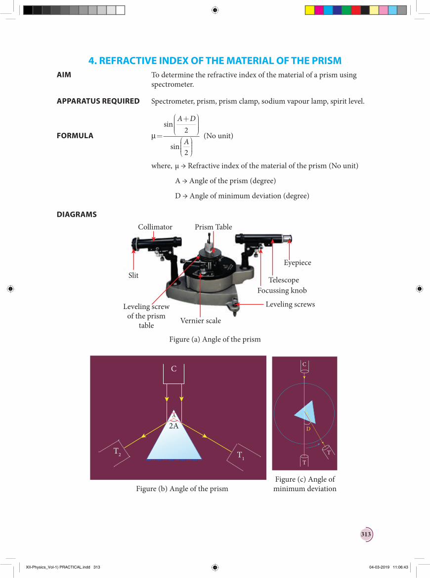
DIAGRAMS
C
2AA
T2 T1
Figure (b) Angle of the prismFigure (c) Angle of
minimum deviation
D
C
T
T
Figure (a) Angle of the prism
Vernier scale
Leveling screwsLeveling screwof the prism
table
Slit
Collimator Prism Table
Eyepiece
TelescopeFocussing knob
XII-Physics_Vol-1) PRACTICAL.indd 313 04-03-2019 11:06:43
314
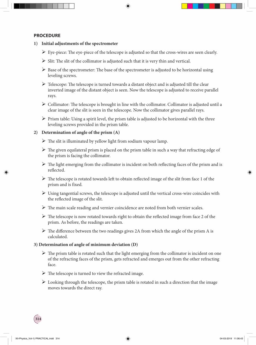
PROCEDURE
1) Initial adjustments of the spectrometer
Eye-piece: The eye-piece of the telescope is adjusted so that the cross-wires are seen clearly.
Slit: The slit of the collimator is adjusted such that it is very thin and vertical.
Base of the spectrometer: The base of the spectrometer is adjusted to be horizontal using leveling screws.
Telescope: The telescope is turned towards a distant object and is adjusted till the clear inverted image of the distant object is seen. Now the telescope is adjusted to receive parallel rays.
Collimator: The telescope is brought in line with the collimator. Collimator is adjusted until a clear image of the slit is seen in the telescope. Now the collimator gives parallel rays.
Prism table: Using a spirit level, the prism table is adjusted to be horizontal with the three leveling screws provided in the prism table.
2) Determination of angle of the prism (A)
The slit is illuminated by yellow light from sodium vapour lamp.
The given equilateral prism is placed on the prism table in such a way that refracting edge of the prism is facing the collimator.
The light emerging from the collimator is incident on both reflecting faces of the prism and is reflected.
The telescope is rotated towards left to obtain reflected image of the slit from face 1 of the prism and is fixed.
Using tangential screws, the telescope is adjusted until the vertical cross-wire coincides with the reflected image of the slit.
The main scale reading and vernier coincidence are noted from both vernier scales.
The telescope is now rotated towards right to obtain the reflected image from face 2 of the prism. As before, the readings are taken.
The difference between the two readings gives 2A from which the angle of the prism A is calculated.
3) Determination of angle of minimum deviation (D)
The prism table is rotated such that the light emerging from the collimator is incident on one of the refracting faces of the prism, gets refracted and emerges out from the other refracting face.
The telescope is turned to view the refracted image.
Looking through the telescope, the prism table is rotated in such a direction that the image moves towards the direct ray.
XII-Physics_Vol-1) PRACTICAL.indd 314 04-03-2019 11:06:43
315
At one particular position, the refracted ray begins to retrace its path. The position where the refracted image returns is the position of minimum deviation.
The telescope is fixed in this position and is adjusted until the vertical cross-wire coincides with the refracted image of the slit.
The readings are taken from both vernier scales.
The prism is now removed and the telescope is rotated to obtain the direct ray image and the readings are taken.
The readings are tabulated and the difference between these two readings gives the angle of minimum deviation D.
From the values of A and D, the refractive index of the material of the glass prism is deter-mined.
Least count
1 MSD = 30′
Number of vernier scale divisions = 30
For spectrometer, 30 vernier scale divisions will cover 29 main scale divisions.
∴ 30 VSD = 29 MSD
Or 1 VSD = 29 / 30 MSD
Least count (LC) = 1 MSD – 1 VSD
= 1 / 30 MSD
= 1′
OBSERVATION
Table 1 To find the angle of the prism (A)
ImageVernier A (Degree) Vernier B (Degree)
MSR VSC TR MSR VSC TR
Reflected image from face 1
Reflected image from face 2
Difference 2A
Mean 2A =
Mean A =
XII-Physics_Vol-1) PRACTICAL.indd 315 04-03-2019 11:06:43

316
Table 2 To find the angle of minimum deviation (D)
ImageVernier A (Degree) Vernier B (Degree)
MSR VSC TR MSR VSC TR
Refracted image
Direct image
Difference D
Mean D =
RESULT
1. Angle of the Prism (A) = ............ (degree)
2. Angle of the minimum deviation of the prism (D) =............. (degree)
3. Refractive index of the material of the Prism (μ) =............. (No unit)
Note:
i) Once initial adjustments are done, spectrometer should not be disturbed.
ii) Total reading TR = MSR + (VSC × LC)
Where
MSR → Main Scale Reading
VSC → Vernier Scale Coincidence
LC → Least count (= 1′)
XII-Physics_Vol-1) PRACTICAL.indd 316 04-03-2019 11:06:43
317
5. WAVELENGTH OF THE CONSTITUENT COLOURS OF A COMPOSITE LIGHT USING DIFFRACTION GRATING AND SPECTROMETER
AIM To find the wavelength of the constituent colours of a composite light using diffraction grating and spectrometer.
APPARATUS REQUIRED Spectrometer, mercury vapour lamp, diffraction grating, grating table, and spirit level.
FORMULA λθ
=sinnN
å
where, λ → Wavelength of the constituent colours of a composite light (å)
N → Number of lines per metre length of the given grating (No unit) (the value of N for the grating is given)
n → Order of the diffraction (No unit)
θ → Angle of diffraction (degree)
DIAGRAMSC
T
C
T
C
TG 45°
C
T
G
Figure (a) Normal incidence
Figure (b) Angle of diffraction
C
T
G
B BG GR RY Y
PROCEDURE1) Initial adjustments of the spectrometer
Eye-piece: The eye-piece of the telescope is adjusted so that the cross-wires are seen clearly.
Slit: The slit of the collimator is adjusted such that it is very thin and vertical.
Base of the spectrometer: The base of the spectrometer is adjusted to be horizontal using leveling screws.
(1) (2) (3) (4)
XII-Physics_Vol-1) PRACTICAL.indd 317 04-03-2019 11:06:44

318
Telescope: The telescope is turned towards a distant object and is adjusted till the clear image of the distant object is seen. Now the telescope is adjusted to receive parallel rays.
Collimator: The telescope is brought in line with the collimator. Collimator is adjusted until a clear image of the slit is seen in the telescope. Now the collimator gives parallel rays.
Grating table: Using a spirit level, the grating table is adjusted to be horizontal with the three leveling screws provided in the grating table.
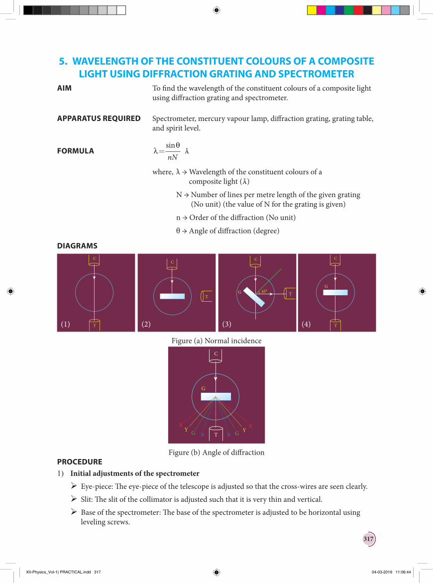
2) Adjustment of the grating for normal incidence
The slit is illuminated with a composite light (white light) from mercury vapour lamp.
The telescope is brought in line with the collimator. The vertical cross-wire is made to coin-cide with the image of the slit (Figure (a)1).
The vernier disc alone is rotated till the vernier scale reads 00 - 1800 and is fixed. This is the reading for the direct ray.
The telescope is then rotated (anti-clockwise) through an angle of 900 and fixed (Figure (a)2).
Now the plane transmission grating is mounted on the grating table.
The grating table alone is rotated so that the light reflected from the grating coincides with vertical cross-wire of the telescope. The reflected image is white in colour (Figure (a)3).
Now the vernier disc is released. The vernier disc along with grating table is rotated through an angle of 450 in the appropriate direction such that the light from the collimator is incident normally on the grating (Figure (a)4).
3) Determination of wave length of the constituent colours of the mercury spectrum
The telescope is released and is brought in line with the collimator to receive central direct image. This undispersed image is white in colour.
The diffracted images of the slit are observed on either side of the direct image.
The diffracted image consists of the prominent colours of mercury spectrum in increasing order of wavelength.
The telescope is turned to any one side (say left) of direct image to observe first order dif-fracted image.
The vertical cross-wire is made to coincide with the prominent spectral lines (violet, blue, yellow and red) and the readings of both vernier scales for each case are noted.
Now the telescope is rotated to the right side of the direct image and the first order image is observed.
The vertical cross-wire is made to coincide with the same prominent spectral lines and the readings of both vernier scales for each case are again noted.
The readings are tabulated.
The difference between these two readings gives the value of 2θ for the particular spectral line.
The number of lines per metre length of the given grating N is noted from the grating.
From the values of N, n and θ, the wave length of the prominent colours of the mercury light is determined using the given formula.
XII-Physics_Vol-1) PRACTICAL.indd 318 04-03-2019 11:06:44

319
OBSERVATION
To find the wave length of prominent colours of the mercury spectrum C
olou
r of
Ligh
t
Diffracted Ray Reading (Degree)Difference
2θ
(Degree)
θ
(Degree)Left Right
Vernier A Vernier B Vernier A Vernier B
MSR
VSC TR MSR
VSC TR MSR
VSC TR MSR
VSC TR
VER
A
VER
B
Mea
n
Blue
Green
Yellow
Red
CALCULATION
(i) For blue, λθ
=sinnN
, (ii) For green, λθ
=sinnN
(iii) For yellow, λθ
=sinnN
, (iv) For red, λθ
=sinnN
RESULT
1. The wavelength of blue line = ----------------m
2. The wavelength of green line = ------------------m
3. The wavelength of yellow line = ----------------m
4. The wavelength of red line = ----------------m
Note:
i) Once initial adjustments are done, spectrometer should not be disturbed.
ii) Total reading TR = MSR + (VSC × LC)
Where
MSR → Main Scale Reading
VSC → Vernier Scale Coincidence
LC → Least count (= 1′)
XII-Physics_Vol-1) PRACTICAL.indd 319 04-03-2019 11:06:44
320
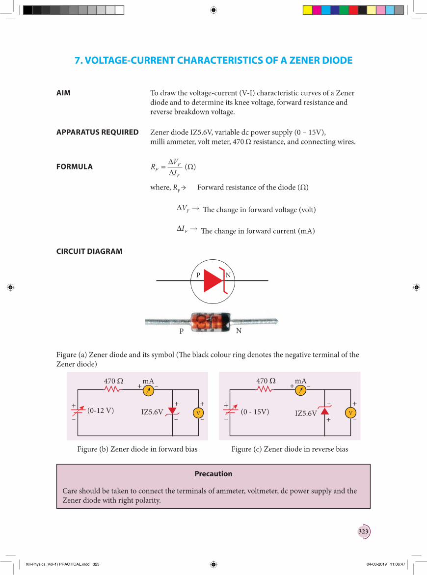
6. VOLTAGE-CURRENT CHARACTERISTICS OF A PN JUNCTION DIODE
AIM To draw the voltage-current (V- I) characteristics of the PN junction diode and to determine its knee voltage and forward resistance.
APPARATUS REQUIRED PN junction diode (IN4007), variable DC power supply, milli-ammeter, micro-ammeter, voltmeter, resistance and connecting wires.
FORMULA R VIFF
F
= ∆∆
(Ω)
where, RF → Forward resistance of the diode (Ω)
∆VF ® The change in forward voltage (volt)
∆IF ® The change in forward current (mA)
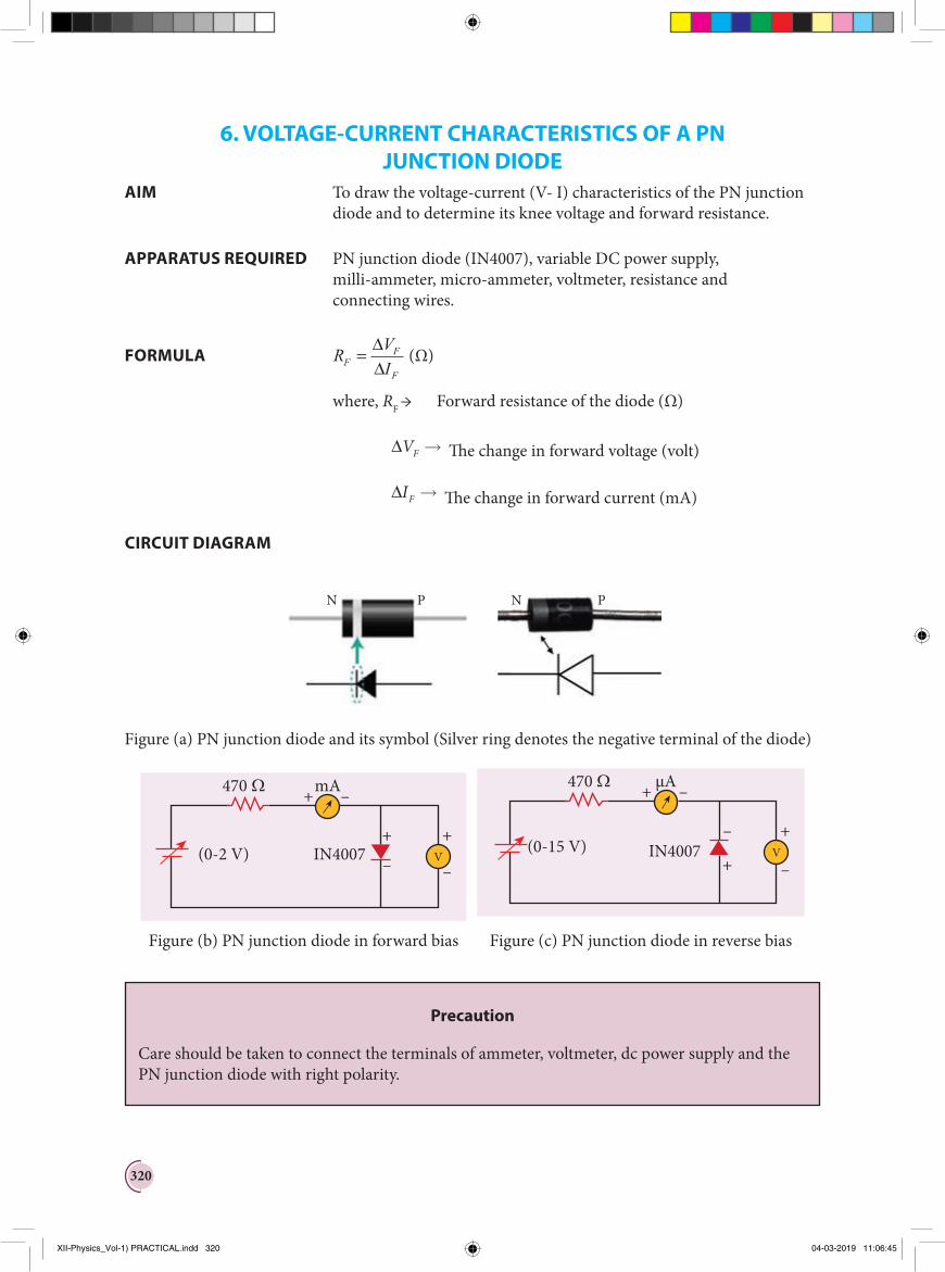
CIRCUIT DIAGRAM
N NP P
Figure (a) PN junction diode and its symbol (Silver ring denotes the negative terminal of the diode)
Figure (b) PN junction diode in forward bias
470 mA+
+ +
–
– –(0-2 V) IN4007 V
Figure (c) PN junction diode in reverse bias
470 µA+
+
+
–
–
–(0-15 V) IN4007 V
Precaution
Care should be taken to connect the terminals of ammeter, voltmeter, dc power supply and the PN junction diode with right polarity.
XII-Physics_Vol-1) PRACTICAL.indd 320 04-03-2019 11:06:45
321
PROCEDURE
i) Forward bias characteristics
• In the forward bias, the P- region of the diode is connected to the positive terminal and N-region to the negative terminal of the DC power supply.
• The connections are given as per the circuit diagram.
• The voltage across the diode can be varied with the help of the variable DC power supply.
• The forward voltage (VF) across the diode is increased from 0.1 V in steps of 0.1 V up to 0.8|V and the forward current (IF) through the diode is noted from the milli-ammeter. The readings are tabulated.
• The forward voltage VF and the forward current IF are taken as positive.
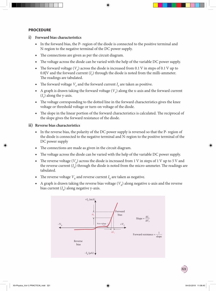
• A graph is drawn taking the forward voltage (VF) along the x-axis and the forward current (IF) along the y-axis.
• The voltage corresponding to the dotted line in the forward characteristics gives the knee voltage or threshold voltage or turn-on voltage of the diode.
• The slope in the linear portion of the forward characteristics is calculated. The reciprocal of the slope gives the forward resistance of the diode.
ii) Reverse bias characteristics
• In the reverse bias, the polarity of the DC power supply is reversed so that the P- region of the diode is connected to the negative terminal and N-region to the positive terminal of the DC power supply
• The connections are made as given in the circuit diagram.
• The voltage across the diode can be varied with the help of the variable DC power supply.
• The reverse voltage (VR) across the diode is increased from 1 V in steps of 1 V up to 5 V and the reverse current (IR) through the diode is noted from the micro-ammeter. The readings are tabulated.
• The reverse voltage VR and reverse current IR are taken as negative.
• A graph is drawn taking the reverse bias voltage (VR) along negative x-axis and the reverse bias current (IR) along negative y-axis.
(µA)
(mA)
Knee voltage
Reverse bias
Forwardbias
+VF
+IF
–IR
–VR
Slope∆=∆
F
F
IV
1Forward resistance
slope=
∆IF
∆VF
XII-Physics_Vol-1) PRACTICAL.indd 321 04-03-2019 11:06:45
322
OBSERVATION
Table 1 Forward bias characteristic curve
S.No.Forward bias voltage VF
(volt)
Forward bias current IF(mA)
Table 2 Reverse bias characteristic curve
S.No.Reverse bias voltage VR
(volt)
Reverse bias current IR(µA)
CALCULATION
(i) Forward resistance RF=
(ii) knee voltage =
RESULT
The V-I characteristics of the PN junction diode are studied.
i) Knee voltage of the PN junction diode =………………V
ii) Forward resistance of the diode =………………Ω
Practical Tips
• The DC power supply voltage should be increased only up to the specified range in the for-ward (0 – 2V) and reverse (0 – 15V) directions. Forward bias offers very low resistance and hence an external resistance of 470Ω is connected as a safety measure.
• The voltage applied beyond this limit may damage the resistance or the diode.
• In the forward bias, the current flow will be almost zero till it crosses the junction potential or knee voltage (approximately 0.7 V). Once knee voltage is crossed, the current increases with the applied voltage.
• The diode voltage in the forward direction should be increased in steps of 0.1 V to a maximum of 0.8 V after the threshold voltage to calculate the forward resistance.
• The diode voltage in the reverse direction is increased in steps of 1 V to a maximum of 5 V. The current must be measured using micro-ammeter as the strength of current in the reverse direction is very less. This is due to the flow of the minority charge carriers called the leakage current.
XII-Physics_Vol-1) PRACTICAL.indd 322 04-03-2019 11:06:47
323
7. VOLTAGE-CURRENT CHARACTERISTICS OF A ZENER DIODE
AIM To draw the voltage-current (V-I) characteristic curves of a Zener diode and to determine its knee voltage, forward resistance and reverse breakdown voltage.
APPARATUS REQUIRED Zener diode IZ5.6V, variable dc power supply (0 – 15V), milli ammeter, volt meter, 470 Ω resistance, and connecting wires.
FORMULA R VIFF
F
= ∆∆
(Ω)
where, RF → Forward resistance of the diode (Ω)
∆VF ® The change in forward voltage (volt)
∆IF ® The change in forward current (mA)
CIRCUIT DIAGRAM
P N
Figure (a) Zener diode and its symbol (The black colour ring denotes the negative terminal of the Zener diode)
Figure (b) Zener diode in forward bias
470 mA+
++ +
–
–– –(0-12 V) IZ5.6V V
Figure (c) Zener diode in reverse bias
470 mA+
+
+ +
–
–
– –(0 - 15V) IZ5.6V V
Precaution
Care should be taken to connect the terminals of ammeter, voltmeter, dc power supply and the Zener diode with right polarity.
P N
XII-Physics_Vol-1) PRACTICAL.indd 323 04-03-2019 11:06:47

324
PROCEDURE
i) Forward bias characteristics
• In the forward bias, the P- region of the diode is connected to the positive terminal and N-re-gion to the negative terminal of the DC power supply.
• The connections are given as per the circuit diagram.
• The voltage across the diode can be varied with the help of the variable DC power supply.
• The forward voltage (VF) across the diode is increased from 0.1V in steps of 0.1V up to 0.8V and the forward current (IF) through the diode is noted from the milli-ammeter. The read-ings are tabulated.
• The forward voltage and the forward current are taken as positive.
• A graph is drawn taking the forward voltage along the x-axis and the forward current along the y-axis.
• The voltage corresponding to the dotted line in the forward characteristics gives the knee voltage or threshold voltage or turn-on voltage of the diode.
• The slope in the linear portion of the forward characteristics is calculated. The reciprocal of the slope gives the forward resistance of the diode.
ii) Reverse bias characteristics
• In the reverse bias, the polarity of the DC power supply is reversed so that the P- region of the diode is connected to the negative terminal and N-region to the positive terminal of the DC power supply
• The connections are made as given in the circuit diagram.
• The voltage across the diode can be varied with the help of the variable DC power supply.
• The reverse voltage (VR) across the diode is increased from 0.5V in steps of 0.5V up to 6V and the reverse current (IR) through the diode is noted from the milli-ammeter. The readings are tabulated.
• Initially, the voltage is increased in steps of 0.5V. When the breakdown region is approxi-mately reached, then the input voltage may be raised in steps of, say 0.1V to find the break-down voltage.
• The reverse voltage and reverse current are taken as negative.
• A graph is drawn taking the reverse bias voltage along negative x-axis and the reverse bias current along negative y-axis.
• In the reverse bias, Zener breakdown occurs at a particular voltage called Zener voltage VZ (~5.6 to 5.8V) and a large amount of current flows through the diode which is the character-istics of a Zener diode.
• The breakdown voltage of the Zener diode is determined from the graph as shown.
XII-Physics_Vol-1) PRACTICAL.indd 324 04-03-2019 11:06:47
325
+IZ
-VZ-VR
-IR
+VF
ZenerBreakdownRegion
ForwardBias
Region
Zenerbreakdown
voltageSlope
∆=∆
F
F
IV
1Forward resistance
slope=
∆IF
∆VF
Knee voltage
OBSERVATION
Table 1 Forward bias characteristic curve
S.No.Forward bias voltage VF
(volt)
Forward bias current IF(mA)
Table 2 Reverse bias characteristic curve
S.No.Reverse bias voltage VR
(volt)
Reverse bias current IR(mA)
CALCULATION
(i) Forward resistance RF=
(ii) knee voltage =
(iii) The breakdown voltage of the Zener diode VZ= ----V
XII-Physics_Vol-1) PRACTICAL.indd 325 04-03-2019 11:06:49

326
RESULT
The V-I characteristics of the Zener diode are studied.
(i) Forward resistance RF=
(ii) knee voltage =
(iii) The breakdown voltage of the Zener diode VZ= ----V
Practical Tips
• The DC power supply voltage should to be increased only up to the specified range in the forward (0 – 2 V) and reverse (0 – 15 V) directions.
• The voltage applied beyond this limit may damage the resistor or the diode.
• Zener diode functions like an ordinary PN junction diode in the forward direction. Hence the forward characteristic is the same for both PN junction diode and Zener diode. Therefore, knee voltage and forward resistance can be determined as explained in the previous experiment.
• Unlike ordinary PN junction diode, the reverse current in Zener diode is measured using milli-ammeter due to the large flow of current.
XII-Physics_Vol-1) PRACTICAL.indd 326 04-03-2019 11:06:49
327
8 CHARACTERISTICS OF A NPN-JUNCTION TRANSISTOR IN COMMON EMITTER CONFIGURATION
AIM To study the characteristics and to determine the current gain of a NPN junction transistor in common emitter configuration.
APPARATUS REQUIRED Transistor - BC 548/BC107, bread board, micro ammeter, milli ammeter, voltmeters, variable DC power supply and connecting wires.
FORMULA r VIiBE
B VCE
= ∆∆
(Ω), r V
IoCE
C IB
=∆∆
(Ω), β=
∆∆
II
C
B VCE
(No unit)
Where, ri → Input impedance (Ω) ∆VBE → The change in base-emitter voltage (volt) ∆IB → The change in base current (µA) ro → Output impedance (Ω) ∆VCE → The change in collector-emitter voltage (volt) ∆ IC → The change in collector current (mA) β → Current gain of the transistor (No unit)
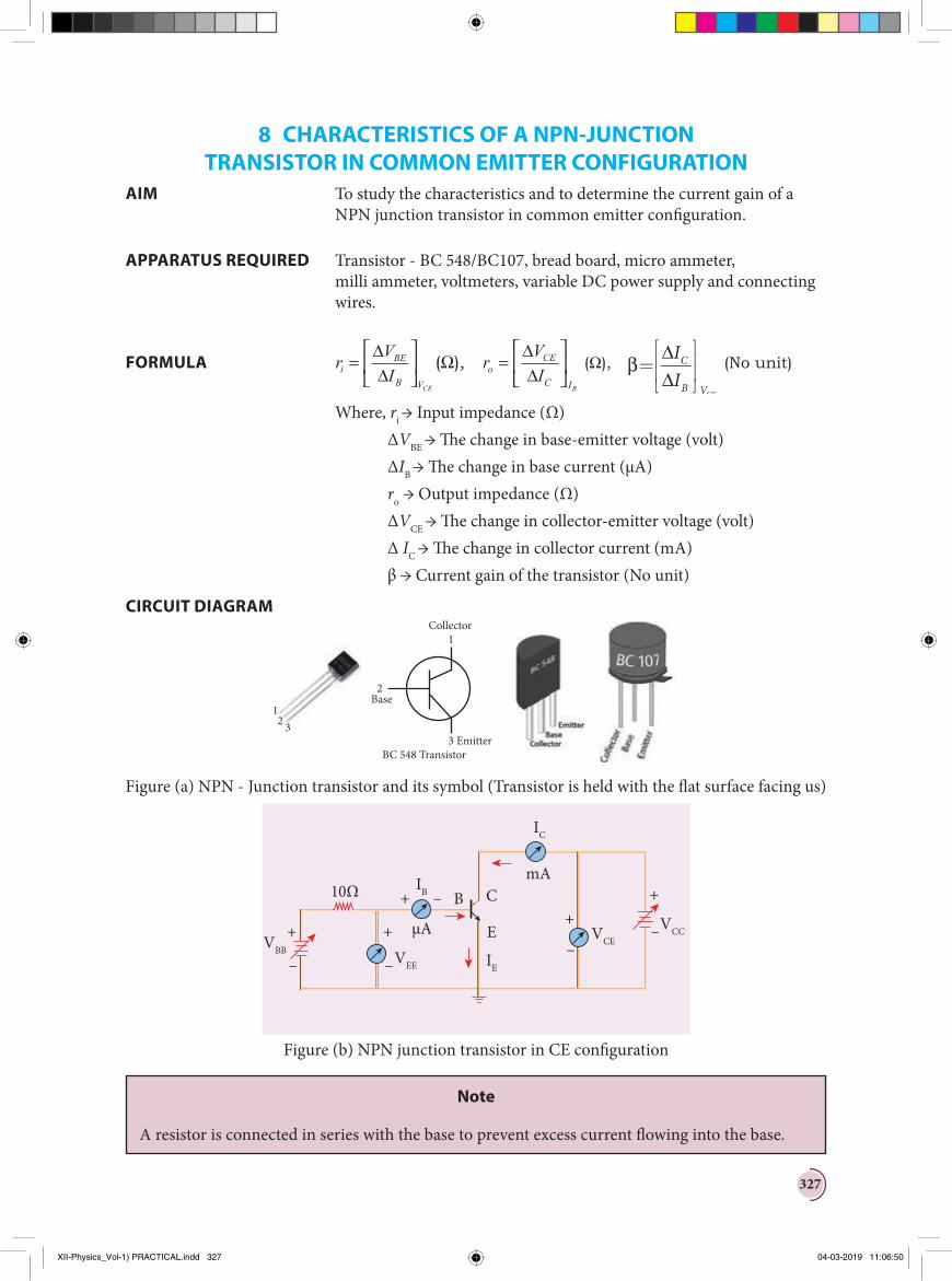
CIRCUIT DIAGRAM
12 3
1
2
3
Collector
Base
EmitterBC 548 Transistor
Figure (a) NPN - Junction transistor and its symbol (Transistor is held with the flat surface facing us)
IE
IB
IC
VEE
VBBVCE
VCC
+ +–
–+
–+
–
+
–
µA
mAB C
E
10Ω
Figure (b) NPN junction transistor in CE configuration
Note
A resistor is connected in series with the base to prevent excess current flowing into the base.
XII-Physics_Vol-1) PRACTICAL.indd 327 04-03-2019 11:06:50
328
Precautions
• Care should be taken to connect the terminals of ammeters, voltmeters, and dc power supplies with right polarity.
• The collector and emitter terminals of the transistor must not be interchanged.
PROCEDURE
The connections are given as shown in the diagram.
The current and voltage at the input and output regions can be varied by adjusting the DC power supply.
(i) Input characteristic curve: VBE vs IB (VCE constant)
• The collector-emitter voltage VCE is kept constant.
• The base-emitter voltage VBE is varied in steps of 0.1V and the corresponding base current (IB) is noted. The readings are taken till VCE reaches a constant value.
• The same procedure is repeated for different values of VCE. The readings are tabulated.
• A graph is plotted by taking VBE along x-axis and IB along y-axis for both the values of VCE.
• The curves thus obtained are called the input characteristics of a transistor.
• The reciprocal of the slope of these curves gives the input impedance of the transistor.
S. No
VCE = 1V VCE = 2V
VBE
(V)
IB
(μA)
VBE
(V)
IB
(μA)
VCE =1V
VCE =2V
IB (µA)
VBE(V)
∆VBE
∆IB
0
Slope∆=∆
B
BE
IV
1Input impedance
slope=
XII-Physics_Vol-1) PRACTICAL.indd 328 04-03-2019 11:06:51
329
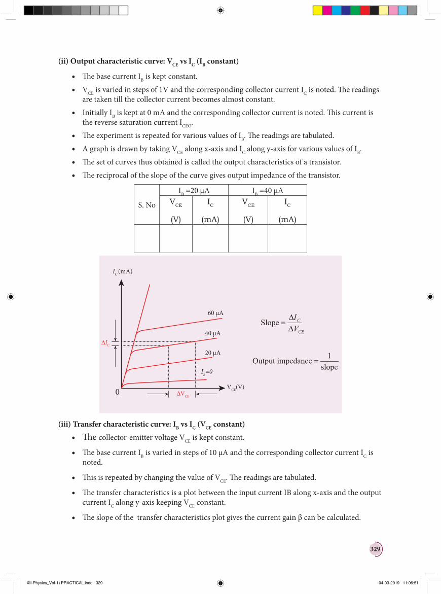
(ii) Output characteristic curve: VCE vs IC (IB constant)
• The base current IB is kept constant.
• VCE is varied in steps of 1V and the corresponding collector current IC is noted. The readings are taken till the collector current becomes almost constant.
• Initially IB is kept at 0 mA and the corresponding collector current is noted. This current is the reverse saturation current ICEO.
• The experiment is repeated for various values of IB. The readings are tabulated.
• A graph is drawn by taking VCE along x-axis and IC along y-axis for various values of IB.
• The set of curves thus obtained is called the output characteristics of a transistor.
• The reciprocal of the slope of the curve gives output impedance of the transistor.
S. No
IB =20 μA IB =40 μAVCE
(V)
IC
(mA)
VCE
(V)
IC
(mA)
IC
IB=0
(mA)
VCE(V)∆VCE
∆IC
0
20 µA
40 µA
60 µASlope
∆=∆
C
CE
IV
1Output impedance
slope=
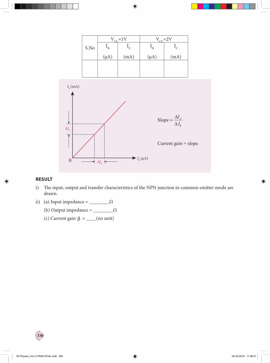
(iii) Transfer characteristic curve: IB vs IC (VCE constant)
• The collector-emitter voltage VCE is kept constant.
• The base current IB is varied in steps of 10 µA and the corresponding collector current IC is noted.
• This is repeated by changing the value of VCE. The readings are tabulated.
• The transfer characteristics is a plot between the input current IB along x-axis and the output current IC along y-axis keeping VCE constant.
• The slope of the transfer characteristics plot gives the current gain β can be calculated.
XII-Physics_Vol-1) PRACTICAL.indd 329 04-03-2019 11:06:51
330
S.No
VCE =1V VCE =2VIB
(μA)
IC
(mA)
IB
(μA)
IC
(mA)
IC (mA)
IB (µA)∆IB
∆IC
0
Slope∆=∆
C
B
II
Current gain = slope
RESULT
i) The input, output and transfer characteristics of the NPN junction in common emitter mode are drawn.
ii) (a) Input impedance = ________Ω
(b) Output impedance = ________Ω
(c) Current gain β = ____(no unit)
XII-Physics_Vol-1) PRACTICAL.indd 330 04-03-2019 11:06:51
331
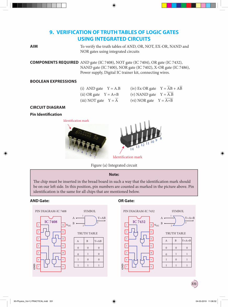
AND Gate:
A
B
Y=AB
Y=AB
SYMBOLPIN DIAGRAM-IC 7408
14
13
12
11
10
9
8
1
2
3
4
5
6
7
GN
D
VCCIC 7408
A
0 0 0
0
00
0 1
1
1 1 1
B
TRUTH TABLE
1
23
OR Gate:
A
B
Y=A+B
Y=A+B
SYMBOLPIN DIAGRAM-IC 7432
14
13
12
11
10
9
8
1
2
3
4
5
6
7
GN
D
VCCIC 7432
A
0 0 0
1
10
0 1
1
1 1 1
B
TRUTH TABLE
1
23
9. VERIFICATION OF TRUTH TABLES OF LOGIC GATES USING INTEGRATED CIRCUITS
AIM To verify the truth tables of AND, OR, NOT, EX-OR, NAND and NOR gates using integrated circuits
COMPONENTS REQUIRED AND gate (IC 7408), NOT gate (IC 7404), OR gate (IC 7432), NAND gate (IC 7400), NOR gate (IC 7402), X-OR gate (IC 7486), Power supply, Digital IC trainer kit, connecting wires.
BOOLEAN EXPRESSIONS
(i) AND gate Y = A.B (iv) Ex OR gate Y = AB + AB (ii) OR gate Y = A+B (v) NAND gate Y = A.B (iii) NOT gate Y = A (vi) NOR gate Y = A+B
CIRCUIT DIAGRAM
Pin IdentificationIdentication mark
1 2 3 4 5 6 7 Identication mark
14 13 12 11 10 9 8
Figure (a) Integrated circuit
Note:
The chip must be inserted in the bread board in such a way that the identification mark should be on our left side. In this position, pin numbers are counted as marked in the picture above. Pin identification is the same for all chips that are mentioned below.
XII-Physics_Vol-1) PRACTICAL.indd 331 04-03-2019 11:06:52
332
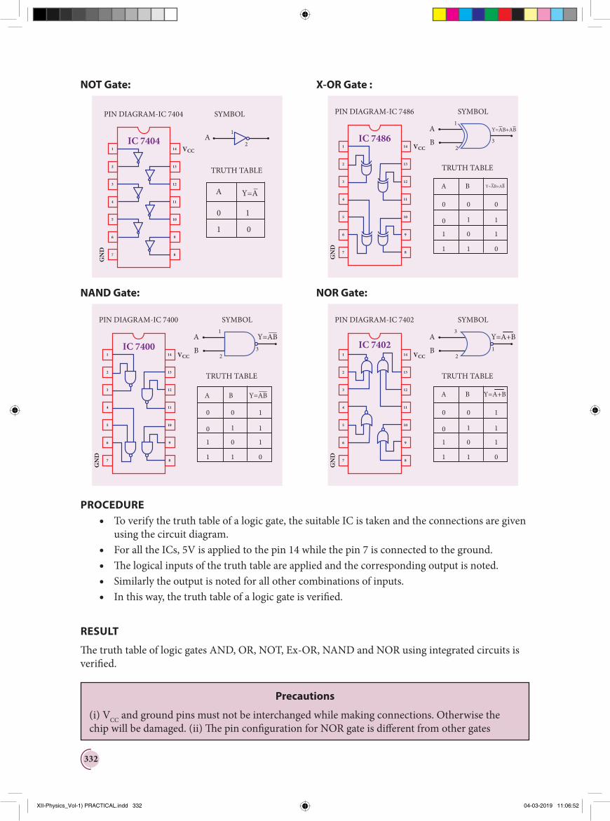
NOT Gate:
SYMBOLPIN DIAGRAM-IC 7404
14
13
12
11
10
9
8
1
2
3
4
5
6
7
GN
D
VCCIC 7404
A
0 1
1 0
TRUTH TABLE
1
2
Y=A
A
NAND Gate:
A
B
Y=AB
Y=AB
SYMBOLPIN DIAGRAM-IC 7400
14
13
12
11
10
9
8
1
2
3
4
5
6
7
GN
D
VCCIC 7400
A
0 0 1
1
10
0 1
1
1 1 0
B
TRUTH TABLE
1
23
X-OR Gate :
A
B
Y=AB+AB
SYMBOLPIN DIAGRAM-IC 7486
14
13
12
11
10
9
8
1
2
3
4
5
6
7
GN
D
VCCIC 7486
A
0 0 0
1
10
0 1
1
1 1 0
B
TRUTH TABLE
1
23
Y=AB+AB
NOR Gate:
A
B
Y=A+B
Y=A+B
SYMBOLPIN DIAGRAM-IC 7402
14
13
12
11
10
9
8
1
2
3
4
5
6
7
GN
D
VCC
IC 7402
A
0 0 1
1
10
0 1
1
1 1 0
B
TRUTH TABLE
3
21
PROCEDURE • To verify the truth table of a logic gate, the suitable IC is taken and the connections are given
using the circuit diagram. • For all the ICs, 5V is applied to the pin 14 while the pin 7 is connected to the ground. • The logical inputs of the truth table are applied and the corresponding output is noted. • Similarly the output is noted for all other combinations of inputs. • In this way, the truth table of a logic gate is verified.
RESULT
The truth table of logic gates AND, OR, NOT, Ex-OR, NAND and NOR using integrated circuits is verified.
Precautions
(i) VCC and ground pins must not be interchanged while making connections. Otherwise the chip will be damaged. (ii) The pin configuration for NOR gate is different from other gates
XII-Physics_Vol-1) PRACTICAL.indd 332 04-03-2019 11:06:52
333
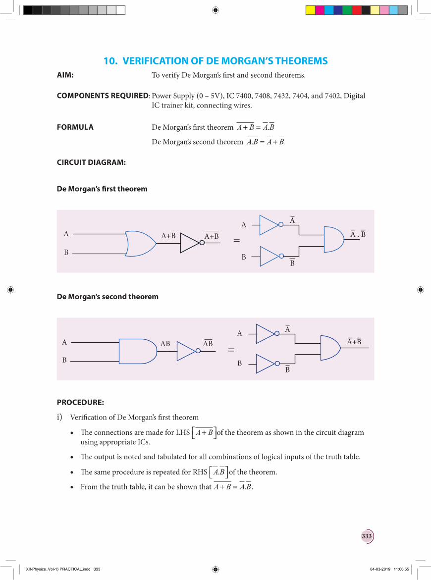
10. VERIFICATION OF DE MORGAN’S THEOREMSAIM: To verify De Morgan’s first and second theorems.
COMPONENTS REQUIRED: Power Supply (0 – 5V), IC 7400, 7408, 7432, 7404, and 7402, Digital IC trainer kit, connecting wires.
FORMULA De Morgan’s first theorem A B A B+ = .
De Morgan’s second theorem A B A B. = +
CIRCUIT DIAGRAM:
De Morgan’s first theorem
AA
B B
A+BA+B =
A
B
A . B
De Morgan’s second theorem
AA
B B
ABAB =
AA+B
B
PROCEDURE:
i) Verification of De Morgan’s first theorem
• The connections are made for LHS A B+ of the theorem as shown in the circuit diagram using appropriate ICs.
• The output is noted and tabulated for all combinations of logical inputs of the truth table.
• The same procedure is repeated for RHS A B. of the theorem.
• From the truth table, it can be shown that A B A B+ = . .
XII-Physics_Vol-1) PRACTICAL.indd 333 04-03-2019 11:06:55

334
ii) Verification of De Morgan’s second theorem
• The connections are made for LHS A B. of the theorem as shown in the circuit diagram using appropriate ICs.
• The output is noted and tabulated for all combinations of logical inputs of the truth table.
• The same procedure is repeated for RHS A B+ of the theorem.
• From the truth table, it can be shown that A B A B. = + .
OBSERVATION
De-Morgan’s first theorem
Truth Table
A B A B+ A B.0 00 11 01 1
De-Morgan’s second theorem
Truth Table
A B A B. A B+0 00 11 01 1
RESULT
De Morgan’s first and second theorems are verified.
Note
The pin diagram for IC 7408, IC 7432 and IC 7404 can be taken from previous experiment
Precautions
VCC and ground pins must not be interchanged while making connections. Otherwise the chip will be damaged.
For the ICs used, 5V is applied to the pin 14 while the pin 7 is connected to the ground.
XII-Physics_Vol-1) PRACTICAL.indd 334 04-03-2019 11:06:57

335
SUGGESTED QUESTIONS FOR THE PRACTICAL EXAMINATION
1. Determine the resistance of a given wire using metre bridge. Also find the radius of the wire using screw gauge and hence determine the specific resistance of the material of the wire. Take at least 4 readings.
2. Determine the value of the horizontal component of the Earth’s magnetic field, using tangent galvanometer. Take at least 4 readings.
3. Determine the value of the horizontal component of the Earth’s magnetic field using the magnetic field produced along the axial line of the carrying-current circular coil. Take at least 2 readings.
4. Using the spectrometer, measure the angle of the given prism and angle of minimum deviation. Hence calculate the refractive index of the material of the prism.
5. Adjust the grating for normal incidence using the spectrometer. Determine the wavelength of green, blue, yellow and red lines of mercury spectrum (The number of lines per metre length of the grating can be noted from the grating).
6. Draw the V-I characteristics of PN junction diode and determine its forward resistance and knee voltage from forward characteristics.
7. Draw the V-I characteristics of Zener diode and determine its forward resistance and knee voltage from forward characteristics. Also find break down voltage of the Zener diode from reverse characteristics.
8. Draw the input and transfer characteristic curves of the given NPN junction transistor in CE mode. Find the input impedance from input characteristics and current gain from transfer characteristics.
9. Draw the output and transfer characteristic curves of the given NPN junction transistor in CE mode. Find the output impedance from output characteristics and current gain from transfer characteristics.
10. Verify the truth table of logic gates AND, NOT, Ex-OR and NOR gates using integrated circuits.
11. Verify the truth table of logic gates OR, NOT, Ex-OR and NOR gates using integrated circuits.
12. Verify De Morgan’s first and second theorems.
Solved examples Competitive Exam corner
XII-Physics_Vol-1) PRACTICAL.indd 335 04-03-2019 11:06:57