Embed Size (px)
Citation preview
Takayuki Ohba, Ph.D.
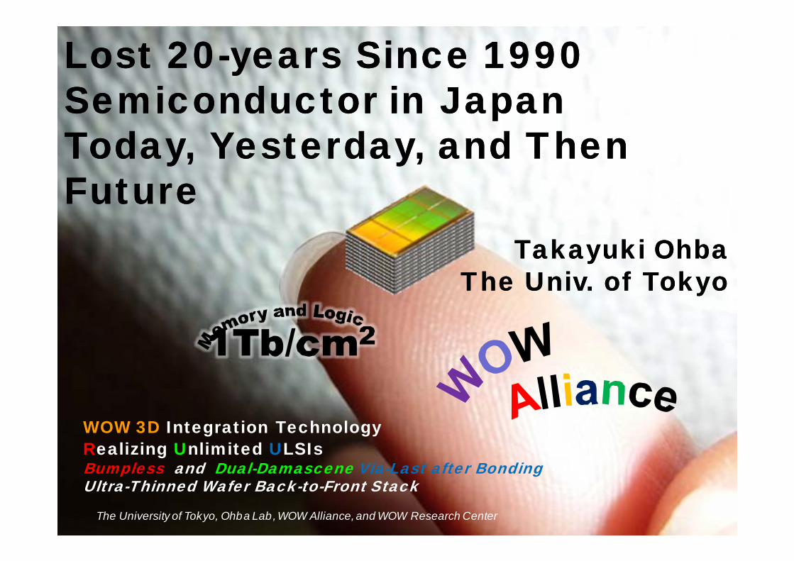
WOW 3D Integration TechnologyRealizing Unlimited ULSIsBumpless and Dual-Damascene Via-Last after BondingUltra-Thinned Wafer Back-to-Front Stack
The University of Tokyo, Ohba Lab, WOW Alliance, and WOW Research Center
Lost 20-years Since 1990Semiconductor in JapanToday, Yesterday, and Then Future
Lost 20-years Since 1990Semiconductor in JapanToday, Yesterday, and Then Future
Takayuki OhbaThe Univ. of Tokyo
Takayuki OhbaThe Univ. of Tokyo
Takayuki Ohba, Ph.D.
Takayuki Ohba, Ph.D.
Takayuki Ohba, Ph.D.
Year
Mar
ket S
hare USA
Japan
EU
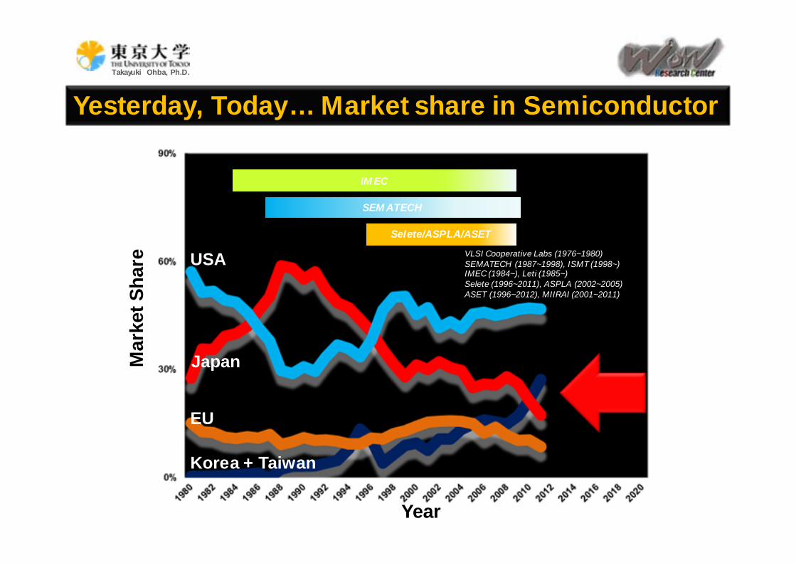
Yesterday, Today… Market share in Semiconductor
VLSI Cooperative Labs (1976~1980)SEMATECH (1987~1998), ISMT (1998~)IMEC (1984~), Leti (1985~)Selete (1996~2011), ASPLA (2002~2005)ASET (1996~2012), MIIRAI (2001~2011)
SEM ATECH
IM EC
Selete/ASPLA/ASET
Korea + Taiwan
Takayuki Ohba, Ph.D.
Inve
stm
ent (
Bill
ion
USD
)
0.7
0.9
0.8 0.9 0.850.6 0.4 1.0
vs GDP (%)
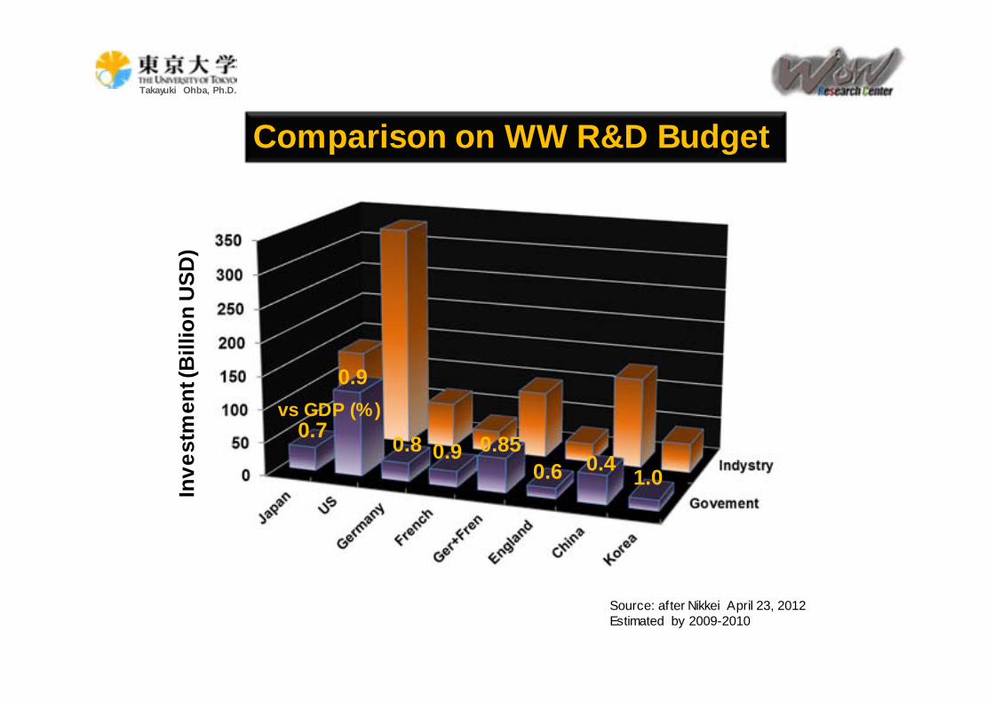
Source: after Nikkei April 23, 2012Estimated by 2009-2010
Comparison on WW R&D Budget
Takayuki Ohba, Ph.D.
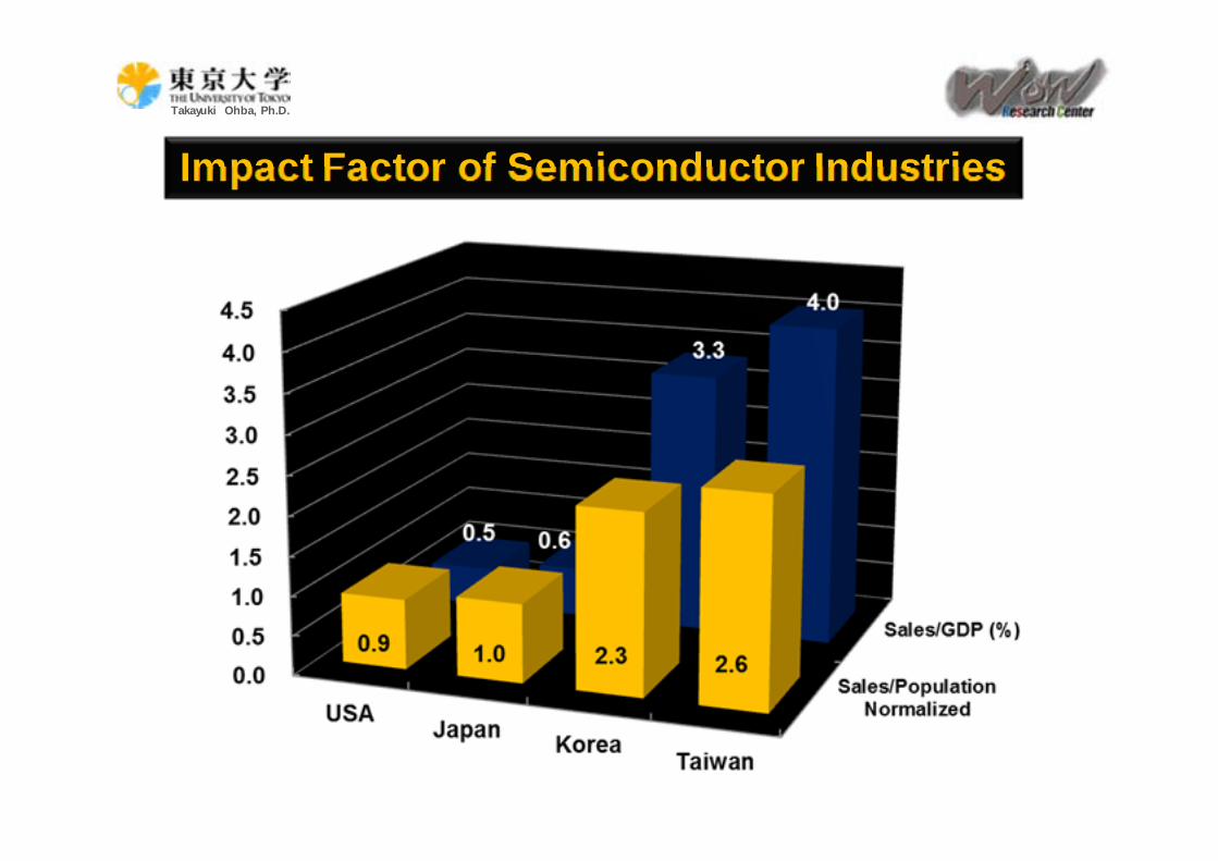
Impact Factor of Semiconductor Industries
Takayuki Ohba, Ph.D.
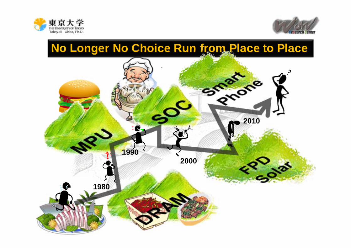
No Longer No Choice Run from Place to Place
1980
19902000
2010
Takayuki Ohba, Ph.D.
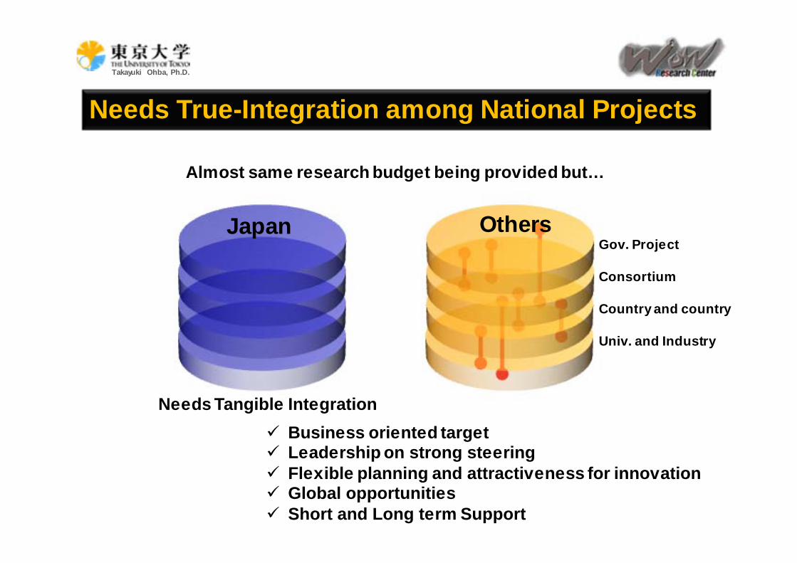
Needs True-Integration among National Projects
Almost same research budget being provided but…
Japan OthersGov. Project
Consortium
Country and country
Univ. and Industry
Business oriented target Leadership on strong steering Flexible planning and attractiveness for innovation Global opportunities Short and Long term Support
Needs Tangible Integration
Takayuki Ohba, Ph.D.
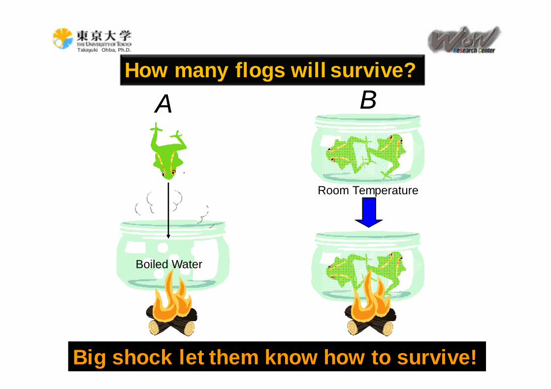
How many flogs will survive?
Boiled Water
Room Temperature
AA BB
Big shock let them know how to survive!
Takayuki Ohba, Ph.D.
40C 100F
50C 120F
60C 140F
70C 160F
80C 180F
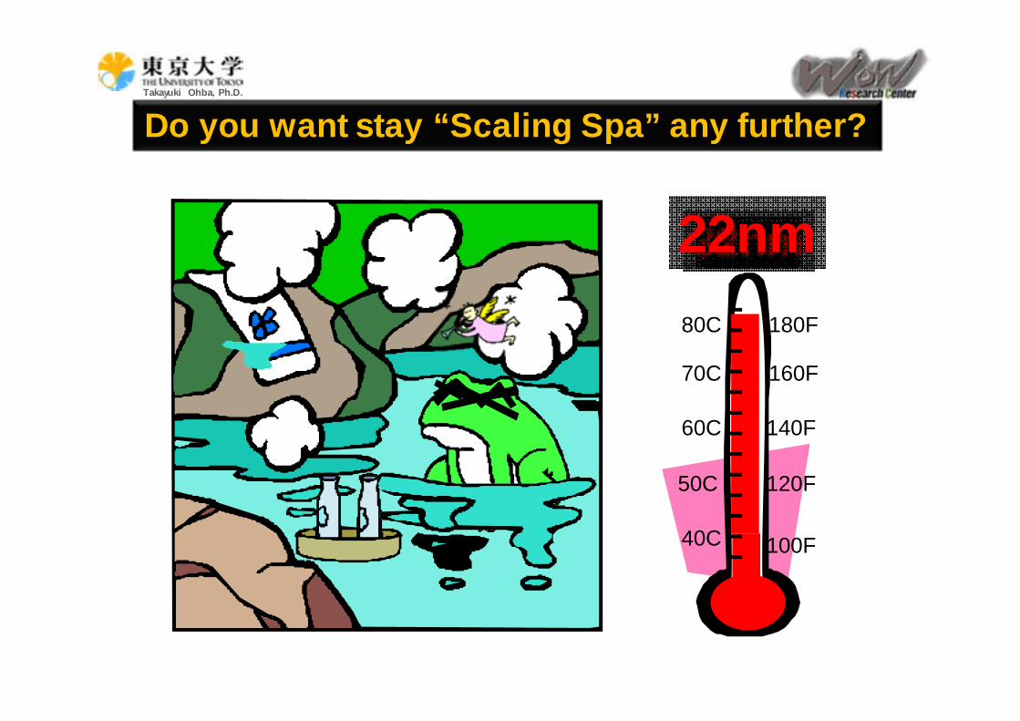
65nm45nm32nm22nm
Do you want stay “Scaling Spa” any further?
Takayuki Ohba, Ph.D.
Takayuki Ohba, Ph.D.
Gro
wth
Rat
e (%
)
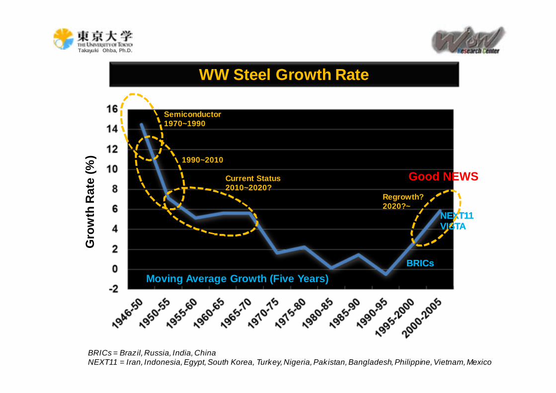
Moving Average Growth (Five Years)BRICsBRICs
NEXT11VISTANEXT11VISTA
BRICs = Brazil, Russia, India, ChinaNEXT11 = Iran, Indonesia, Egypt, South Korea, Turkey, Nigeria, Pakistan, Bangladesh, Philippine, Vietnam, Mexico
Semiconductor1970~1990
1990~2010
Current Status2010~2020?
Regrowth?2020?~
Good NEWS
WW Steel Growth Rate
Takayuki Ohba, Ph.D.
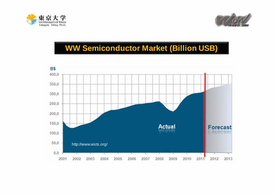
WW Semiconductor Market (Billion USB)
http://www.wsts.org/
Takayuki Ohba, Ph.D.
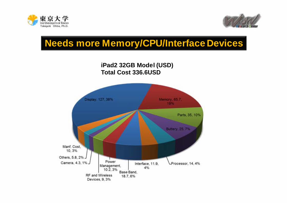
iPad2 32GB Model (USD)Total Cost 336.6USD
Needs more Memory/CPU/Interface Devices
Takayuki Ohba, Ph.D.
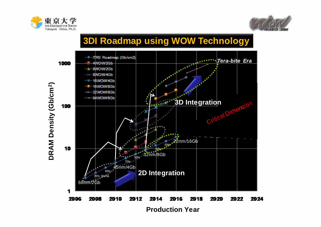
18nm/32Gb
11nm/64Gb
50%
DR
AM
Den
sity
(Gb/
cm2 )
Production Year
2D Integration
3D Integration
3DI Roadmap using WOW Technology
Tera-bite Era
32nm/8Gb
22nm/16Gb70%
50%
68nm/2Gb70% Shrink
45nm/4Gb
50%70%
Takayuki Ohba, Ph.D.
Year
Feat
ure
Size
(m
)
Sale
s (B
illio
n U
SD)
Tr. CD (MPU Printed Gate Length)
3D TSV CD10
5
2
0.8
0.5
3D Based Products
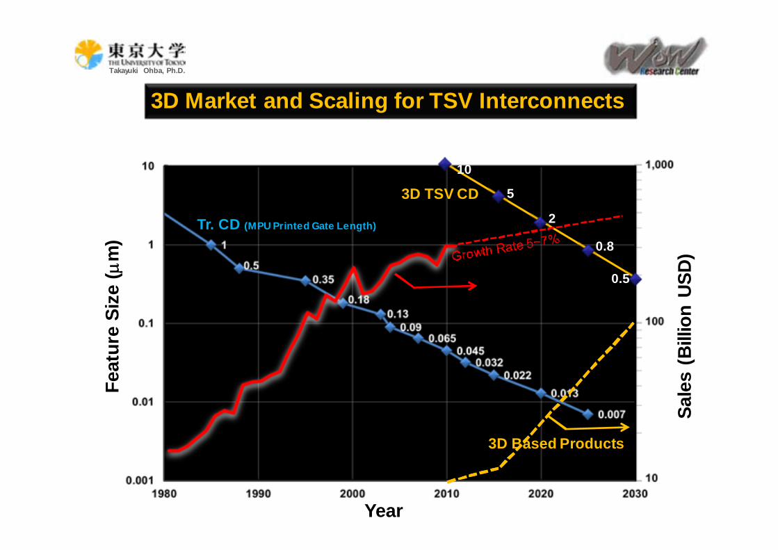
3D Market and Scaling for TSV Interconnects
Takayuki Ohba, Ph.D.
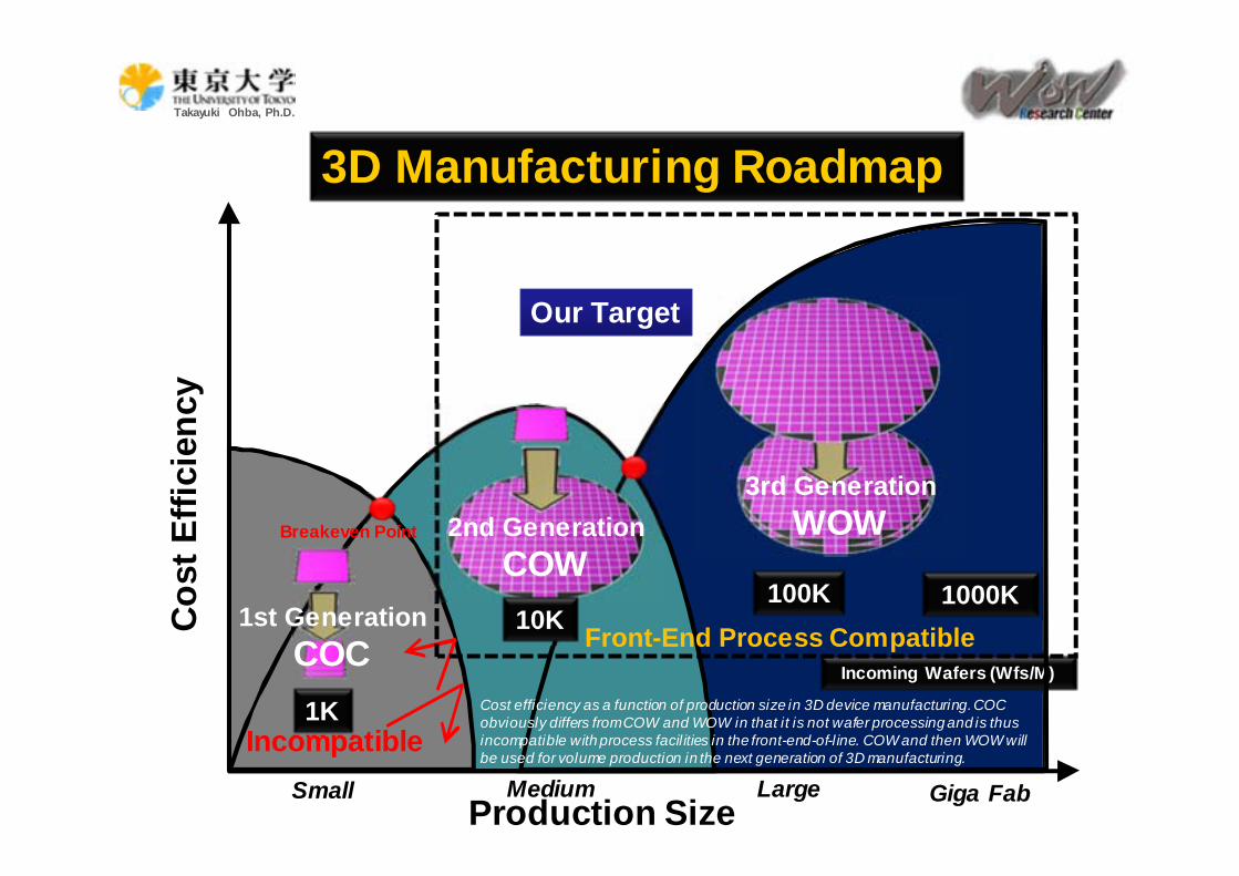
Production Size
3D Manufacturing Roadmap
Our Target
Incompatible
Cos
t Effi
cien
cy
1K
Small Medium Large Giga Fab
Incoming Wafers (Wfs/M)
Front-End Process Compatible
3rd GenerationWOW
100K 1000K
Breakeven Point
1st GenerationCOC
2nd GenerationCOW10K
Cost efficiency as a function of production size in 3D device manufacturing. COC obviously differs from COW and WOW in that it is not wafer processing and is thus incompatible with process facil ities in the front-end-of-l ine. COW and then WOW will be used for volume production in the next generation of 3D manufacturing.
Takayuki Ohba, Ph.D.
Takayuki Ohba, Ph.D.
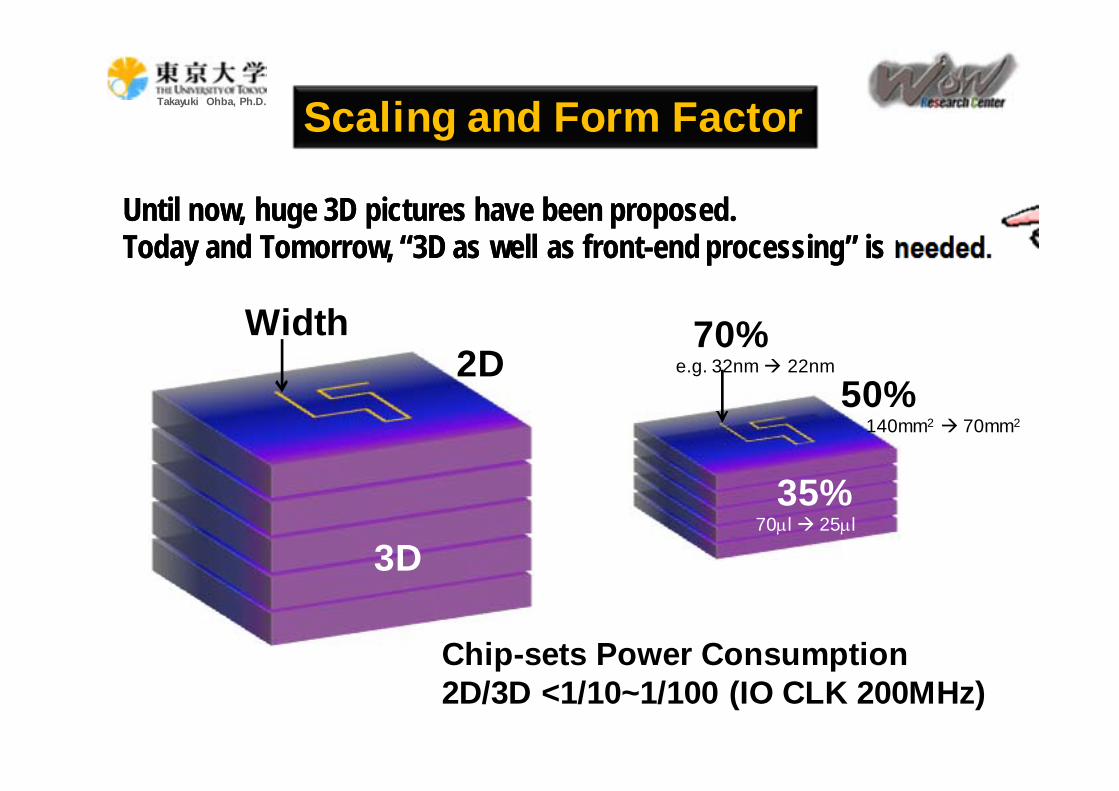
Width2D
3D
70%50%
35%
Scaling and Form Factor
e.g. 32nm 22nm
140mm2 70mm2
70l 25l
Chip-sets Power Consumption2D/3D <1/10~1/100 (IO CLK 200MHz)
Until now, huge 3D pictures have been proposed. Today and Tomorrow, “3D as well as front-end processing” is needed.Until now, huge 3D pictures have been proposed. Today and Tomorrow, “3D as well as front-end processing” is needed.
Takayuki Ohba, Ph.D.
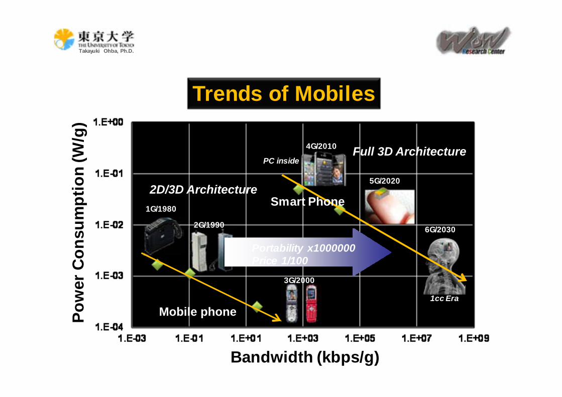
Bandwidth (kbps/g)
Pow
er C
onsu
mpt
ion
(W/g
)
Mobile phone
PC inside
1G/1980
2G/1990
3G/2000
4G/2010
Portability x1000000Price 1/100
5G/2020
6G/2030
2D/3D Architecture
Full 3D Architecture
Trends of Mobiles
1cc Era
Smart Phone
Takayuki Ohba, Ph.D.
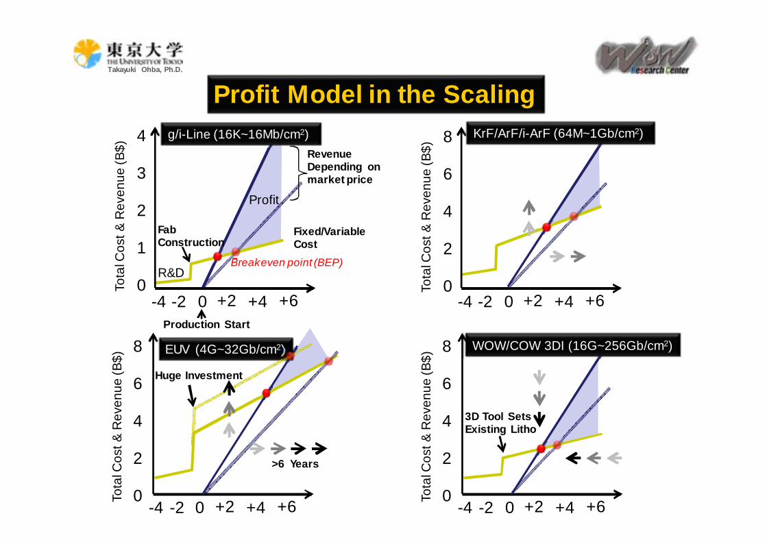
Profit Model in the Scaling
R&D
Profit
0 +2 +4 +6-2-4
Breakeven point (BEP)
0
1
2
3
4To
tal C
ost &
Rev
enue
(B$)
g/i-Line (16K~16Mb/cm2)
Fab Construction
Fixed/Variable Cost
RevenueDepending on market price
Production Start
0 +2 +4 +6-2-40
2
4
6
8
Tota
l Cos
t & R
even
ue (B
$)
WOW/COW 3DI (16G~256Gb/cm2)
3D Tool SetsExisting Litho
0 +2 +4 +6-2-40
2
4
6
8
Tota
l Cos
t & R
even
ue (B
$)
KrF/ArF/i-ArF (64M~1Gb/cm2)
0 +2 +4 +6-2-40
2
4
6
8
Tota
l Cos
t & R
even
ue (B
$)
EUV (4G~32Gb/cm2)
Huge Investment
>6 Years
Takayuki Ohba, Ph.D.
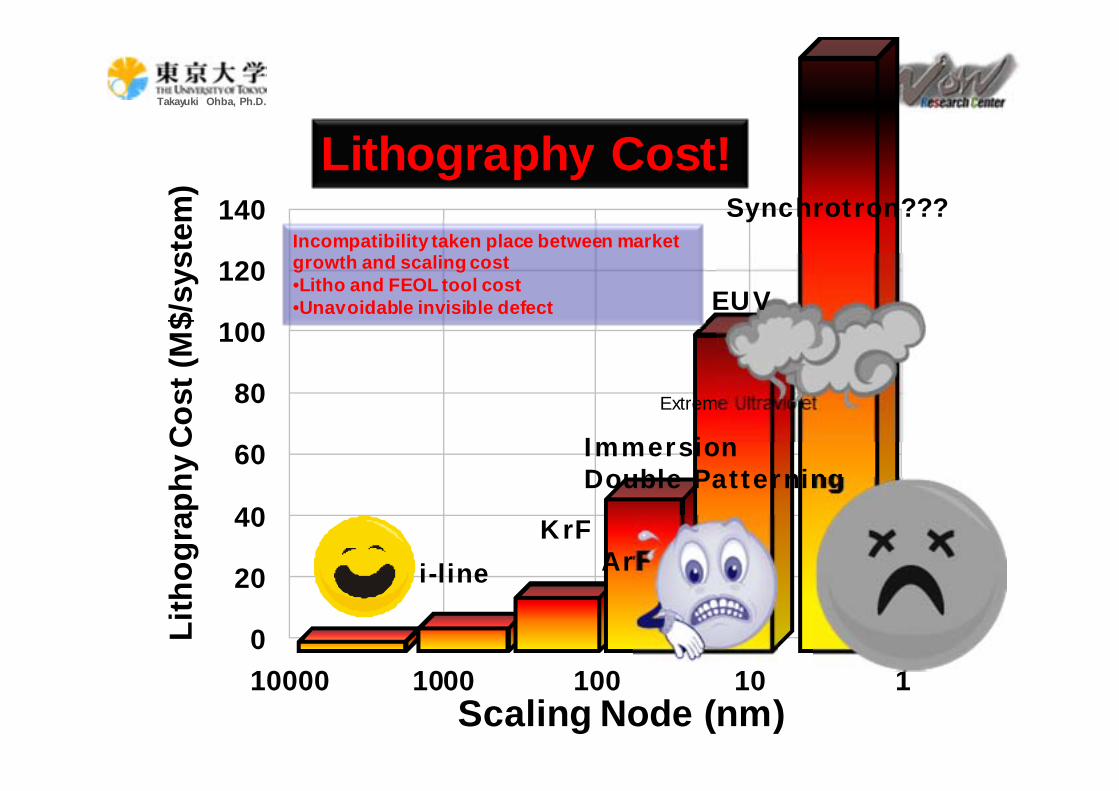
0
20
40
60
80
100
120
140
110100100010000Scaling Node (nm)
Lith
ogra
phy
Cos
t (M
$/sy
stem
)Physics
i-lineKrF
ArF
ImmersionDouble Patterning
Synchrotron???Incompatibility taken place between market growth and scaling cost•Litho and FEOL tool cost•Unavoidable invisible defect
Extreme Ultraviolet
EUV
Lithography Cost!
Takayuki Ohba, Ph.D.
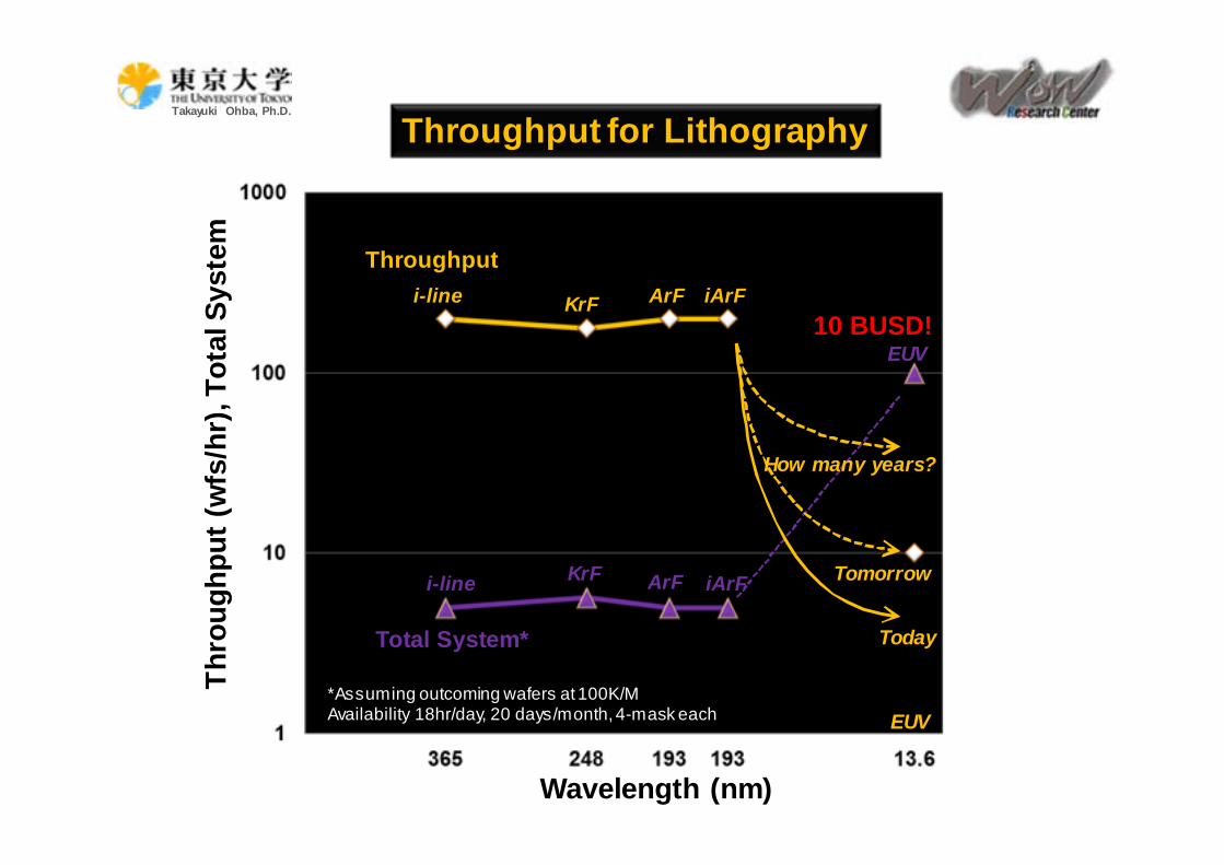
Wavelength (nm)
Thro
ughp
ut (w
fs/h
r), T
otal
Sys
tem
Throughput
Total System*
*Assuming outcoming wafers at 100K/MAvailability 18hr/day, 20 days/month, 4-mask each
Today
Tomorrow
How many years?
Throughput for Lithography
EUV
ArFKrF iArFi-line
EUV
ArFKrF iArFi-line10 BUSD!
Takayuki Ohba, Ph.D.
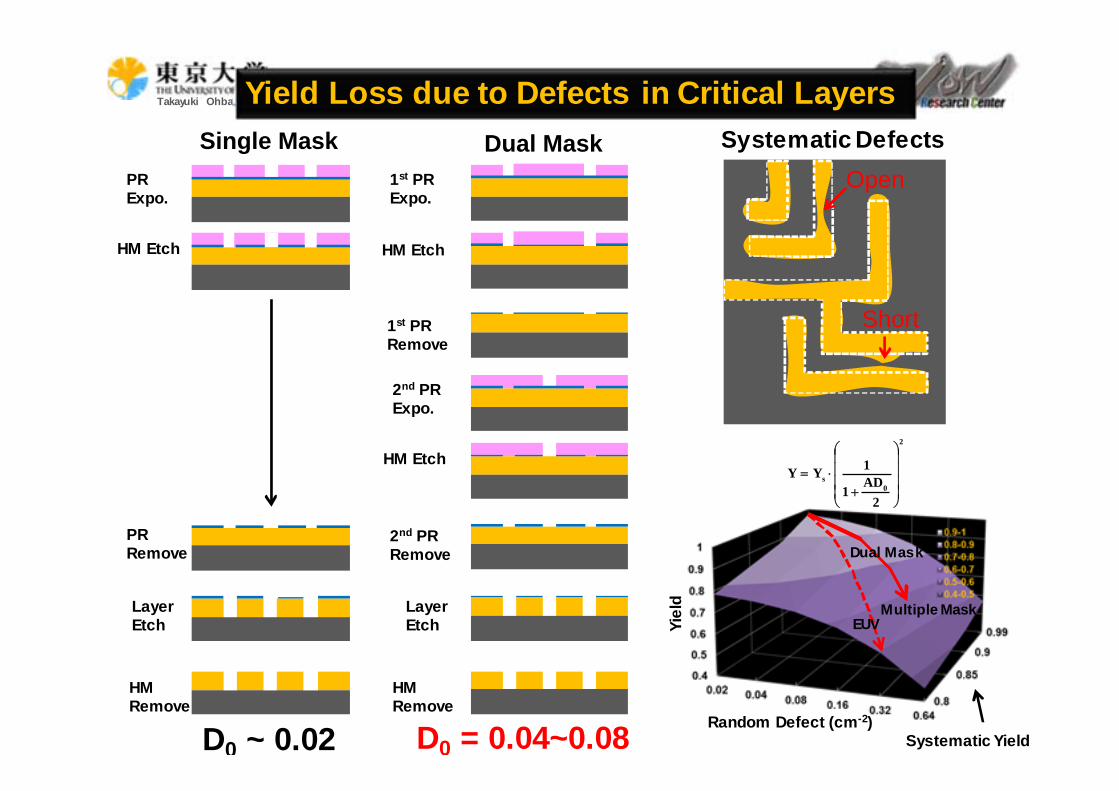
PRExpo.
HM Etch
PRRemove
LayerEtch
HMRemove
Single Mask
D0 ~ 0.02
1st PRExpo.
HM Etch
1st PRRemove
2nd PRExpo.
HM Etch
2nd PRRemove
LayerEtch
HMRemove
Dual Mask
D0 = 0.04~0.08
Yield Loss due to Defects in Critical Layers
Open
Short
Random Defect (cm-2)Systematic Yield
2
0s
2AD
1
1YY
Systematic Defects
Yiel
d Multiple Mask
Dual Mask
EUV
Takayuki Ohba, Ph.D.
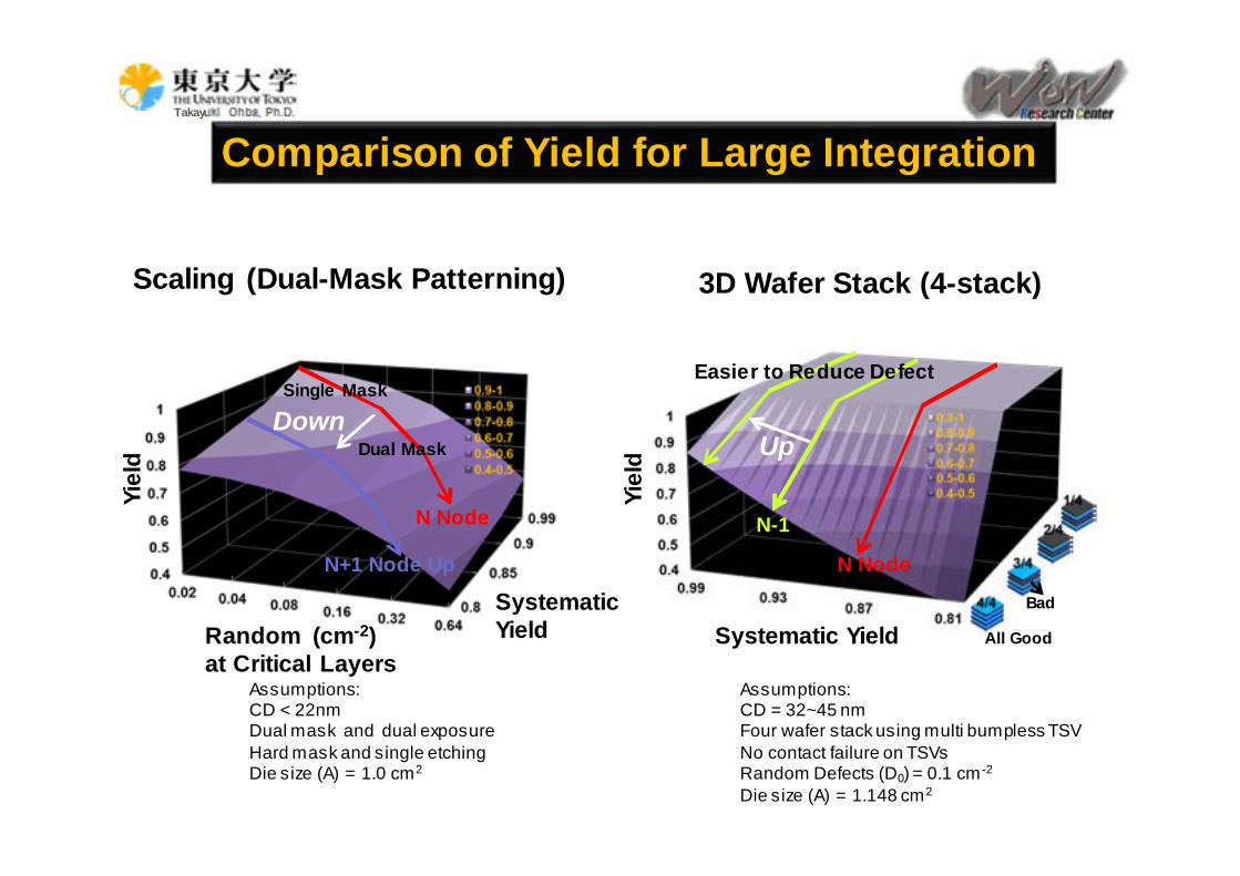
Comparison of Yield for Large IntegrationYi
eld
SystematicYieldRandom (cm-2)
at Critical Layers
Scaling (Dual-Mask Patterning)
Single Mask
Dual Mask
N Node
N+1 Node Up
Assumptions:CD < 22nmDual mask and dual exposureHard mask and single etchingDie size (A) = 1.0 cm2
Down
Assumptions:CD = 32~45 nmFour wafer stack using multi bumpless TSVNo contact failure on TSVsRandom Defects (D0) = 0.1 cm-2
Die size (A) = 1.148 cm2
Yiel
dAll GoodSystematic Yield
3D Wafer Stack (4-stack)
N-1
Easier to Reduce Defect
N Node
Up
Bad
Takayuki Ohba, Ph.D.
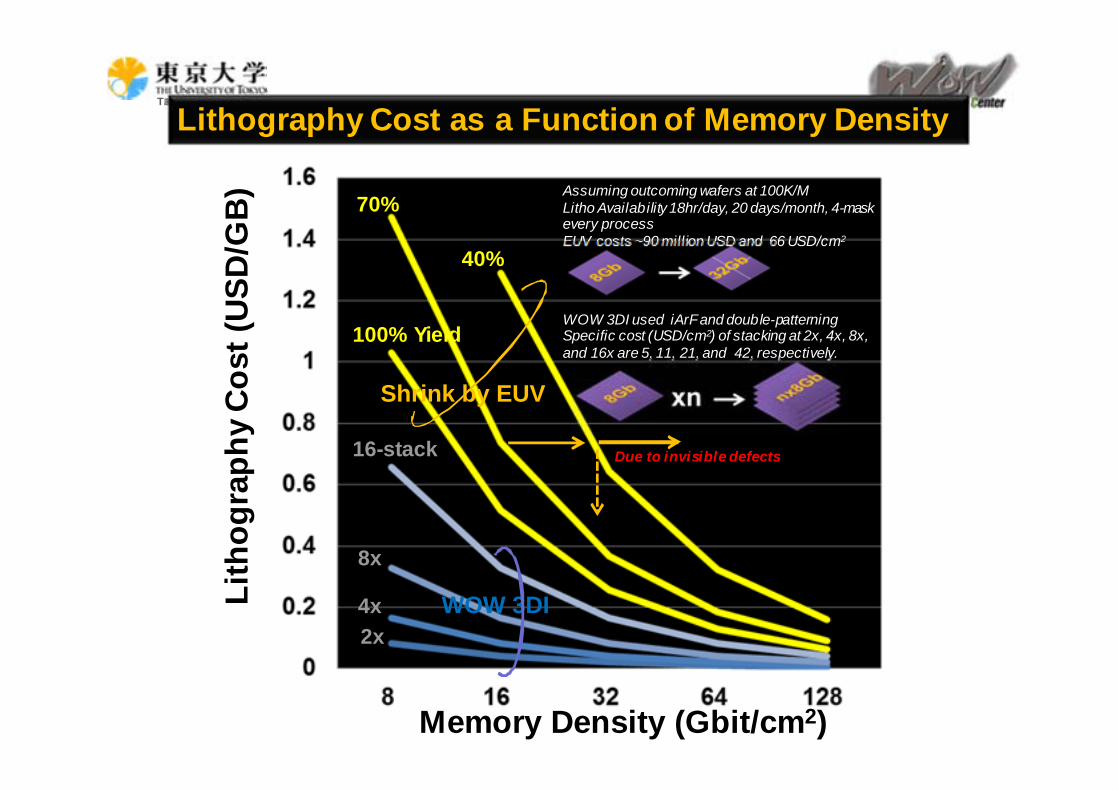
Memory Density (Gbit/cm2)
Lith
ogra
phy
Cos
t (U
SD/G
B)
Shrink by EUV
WOW 3DI
16-stack
8x
4x2x
70%Assuming outcoming wafers at 100K/MLitho Availability 18hr/day, 20 days/month, 4-mask every processEUV costs ~90 million USD and 66 USD/cm2
WOW 3DI used iArFand double-patterningSpecific cost (USD/cm2) of stacking at 2x, 4x, 8x, and 16x are 5, 11, 21, and 42, respectively.
Lithography Cost as a Function of Memory Density
100% Yield
40%
Due to invisible defects
Takayuki Ohba, Ph.D.
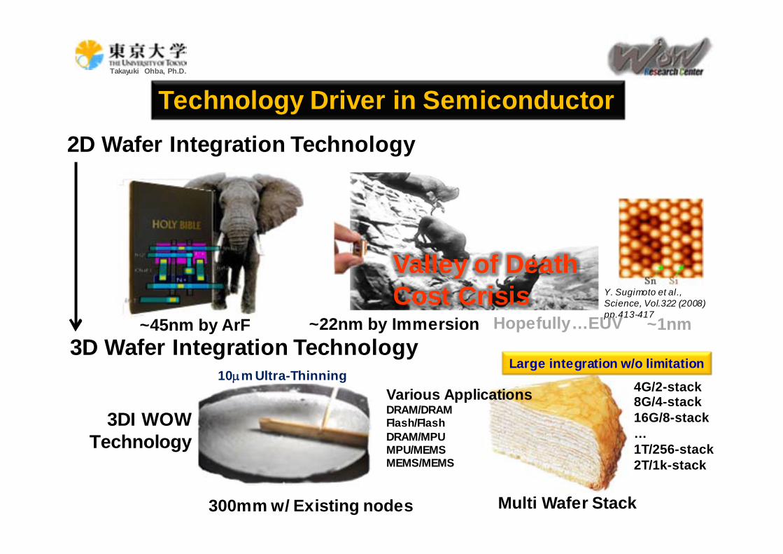
Valley of DeathCost Crisis
2D Wafer Integration Technology
~45nm by ArF3D Wafer Integration Technology
Y. Sugimoto et al., Science, Vol.322 (2008) pp.413-417
~22nm by Immersion Hopefully…EUV ~1nm
Technology Driver in Semiconductor
300mm w/ Existing nodes Multi Wafer Stack
10m Ultra-Thinning 4G/2-stack8G/4-stack16G/8-stack …1T/256-stack2T/1k-stack
3DI WOWTechnology
Various ApplicationsDRAM/DRAMFlash/FlashDRAM/MPUMPU/MEMSMEMS/MEMS
Large integration w/o limitation
Takayuki Ohba, Ph.D.
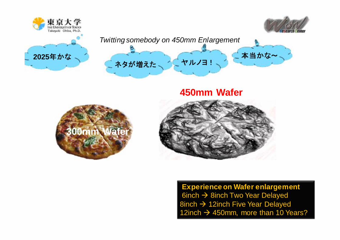
http://ec.europa.eu/commission_2010-2014/geoghegan-quinn/multimedia/photos/201110_photos_en.htm
Experience on Wafer enlargement6inch 8inch Two Year Delayed8inch 12inch Five Year Delayed12inch 450mm, more than 10 Years?
本当かな~ネタが増えた ヤルノヨ!
2025年かな
Twitting somebody on 450mm Enlargement
300mm Wafer
450mm Wafer
Takayuki Ohba, Ph.D.
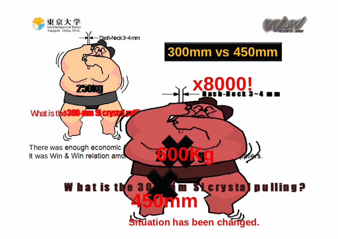
Dash-Neck 3~4 mm
250kg
What is the 300-mm Si crystal pulling?
There was enough economic background and global cooperation.It was Win & Win relation among device manufactures and tool suppliers.600Kg
450mm
x8000!
Situation has been changed.
300mm vs 450mm
Takayuki Ohba, Ph.D.
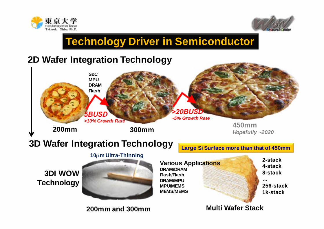
2D Wafer Integration Technology
200mm 300mm 450mmHopefully ~2020
SoCMPUDRAMFlash
Technology Driver in Semiconductor
3D Wafer Integration Technology
200mm and 300mm Multi Wafer Stack
10m Ultra-Thinning Various ApplicationsDRAM/DRAMFlash/FlashDRAM/MPUMPU/MEMSMEMS/MEMS
2-stack4-stack8-stack …256-stack1k-stack
3DI WOWTechnology
Large Si Surface more than that of 450mm
5BUSD>10% Growth Rate
>20BUSD~5% Growth Rate
Takayuki Ohba, Ph.D.
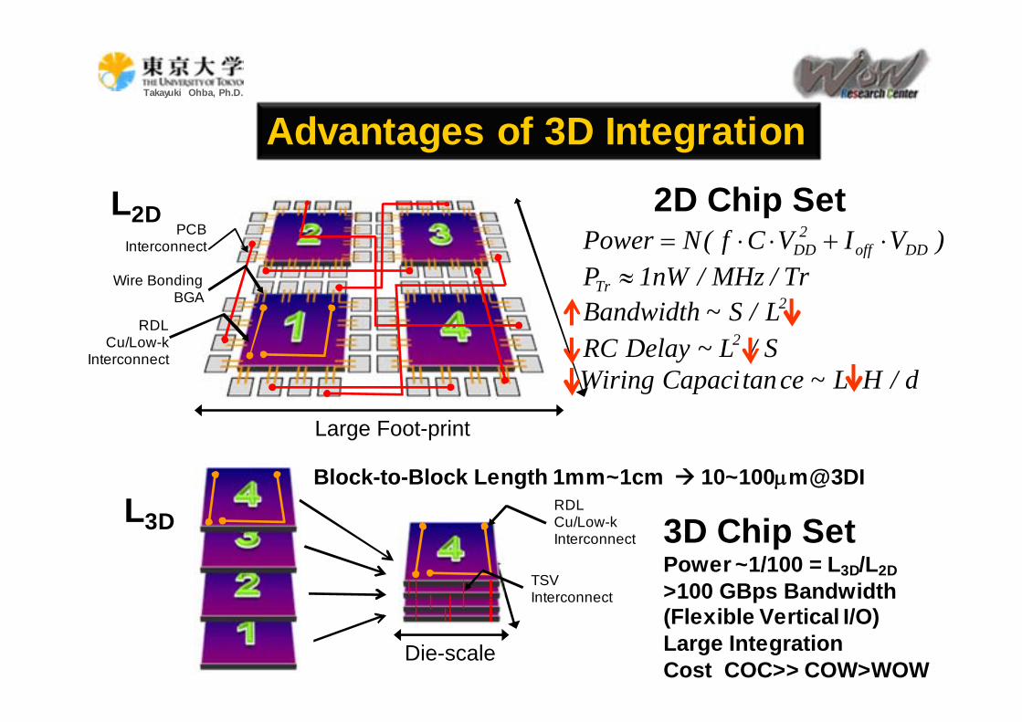
Wire BondingBGA
PCBInterconnect
RDLCu/Low-k
Interconnect
Large Foot-print
2D Chip SetL2D
Advantages of 3D Integration
3D Chip SetPower ~1/100 = L3D/L2D>100 GBps Bandwidth(Flexible Vertical I/O)Large IntegrationCost COC>> COW>WOW
L3D
Die-scale
RDLCu/Low-kInterconnect
TSVInterconnect
Block-to-Block Length 1mm~1cm 10~100m@3DI
d/HL~cetanCapaciWiringS/L~DelayRCL/S~Bandwidth
Tr/MHz/nW1P)VIVCf(NPower
2
2Tr
DDoff2
DD
Takayuki Ohba, Ph.D.Univ. of Tokyo and WOW Alliance
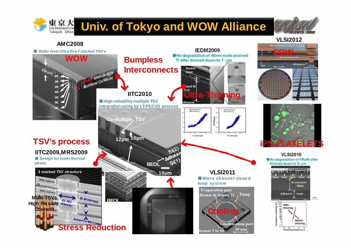
IITC2009,MRS2009■ Design for lower thermalstress
N. Maeda, et al., Proc. of AMC, (2008) p 91
M7
M6
M5M4
M3M2
M1
N. M aeda, e t. a l. AMC2008
AMC2008■ Wafer level Ultra thin 7 stacked TSV’s
10µm
12µm
Cu-Multiple TSV
10µm
BEOL
IITC2010■High reliability multiple TSV integration using by LT-PECVD process
BEOLBEOLBEOL
VLSI2011■Micro channel closed loop system
BumplessInterconnects
TSV’s process
Ultra-Thinning
Multi-TSVsHigh Flexible
Connect
3 stacked TSV structure
WOW
Stress Reduction
Cooling
COW
iPS PLATELETS
VLSI2012
Takayuki Ohba, Ph.D.
CMOS
WOW 3DI
Cu/Low-k
OxidationDiffusionDiffusion
LithographyLithography
EtchingEtching
DepositionDeposition
CMPCMP
Grinding
Probe TestProbe Test
GrindingGrinding
DicingDicing
BondingBonding
MoldingMolding
InspectionInspection
LithographyLithography
EtchingEtching
Deposition
CMP
Waf
er P
roce
ss~1
000
Proc
ess
Step
Pack
agin
g
FEO
LBE
OL
Conventional
StackingStacking
gThinning
gStackingLithography
TSV EtchingTSV Etching
DepositionDeposition
PlanarizationPlanarization
OxidationOxidationDiffusionDiffusion
LithographyLithography
EtchingEtching
DepositionDeposition
CMPCMP
g yLithography
gEtching
DepositionDeposition
CMPCMP
Waf
er P
roce
ss
Pack
agin
gFE
OL
BEO
L
DicingDicing
BondingBonding
MoldingMolding
InspectionInspection
Wafer ProbeWafer Probe
w/ WOW
WO
W3D
Pro
cess
ing
GrindingGrinding
Next Manufacturing Scheme
>30000 Step*
*Assuming 10-stacked 1000-3D Memory sets using 300-mm wafer
~500 Step*
COC 3D Stack
Takayuki Ohba, Ph.D.
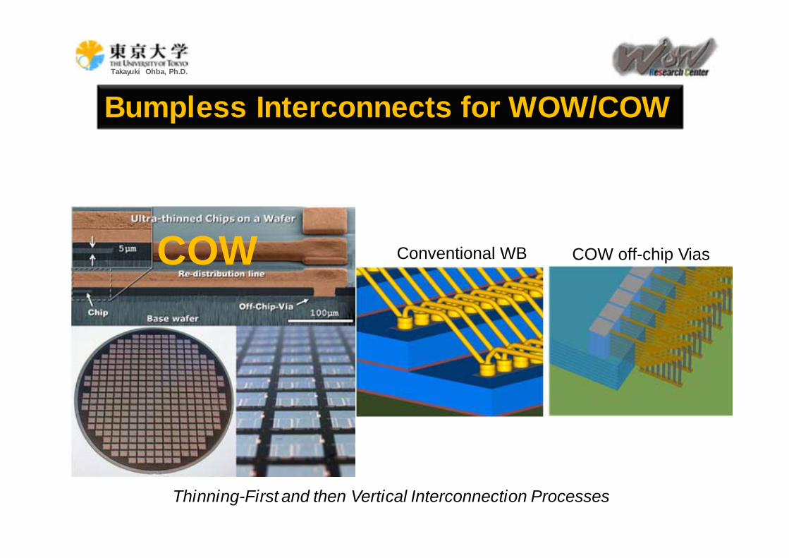
Bumpless Interconnects for WOW/COW
Thinning-First and then Vertical Interconnection Processes
COW Conventional WB COW off-chip Vias
Takayuki Ohba, Ph.D.
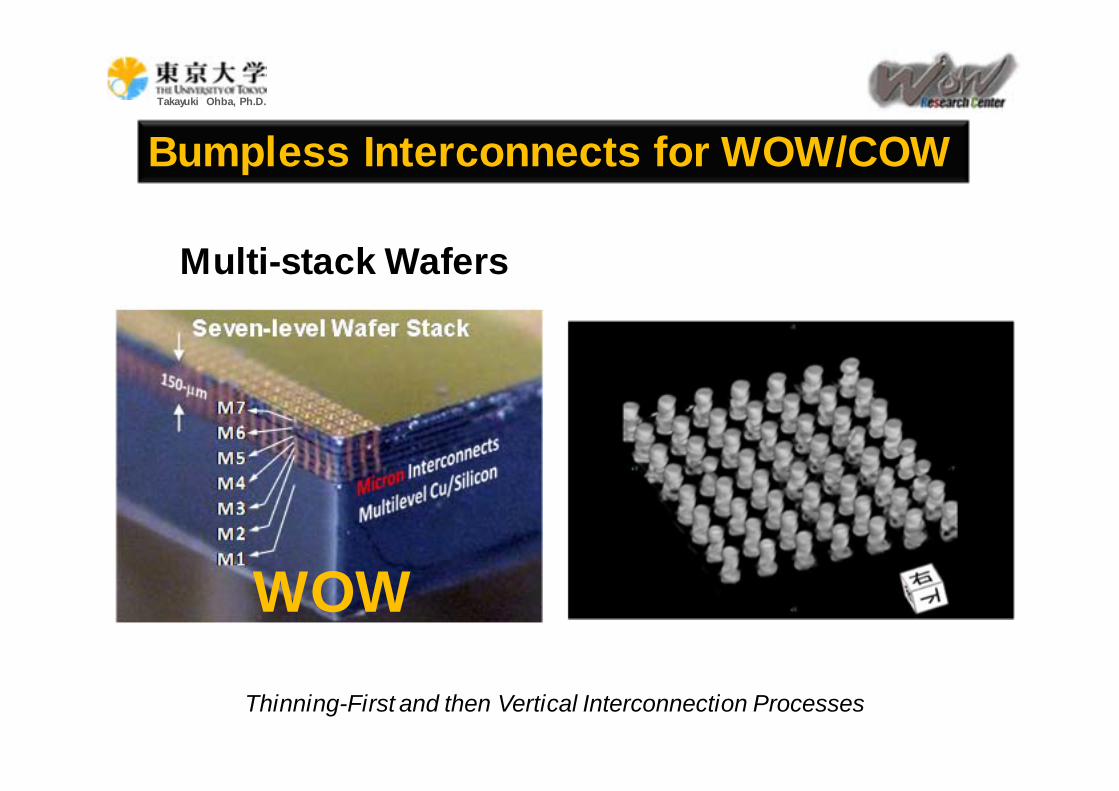
Bumpless Interconnects for WOW/COW
Multi-stack Wafers
Thinning-First and then Vertical Interconnection Processes
WOW
Takayuki Ohba, Ph.D.
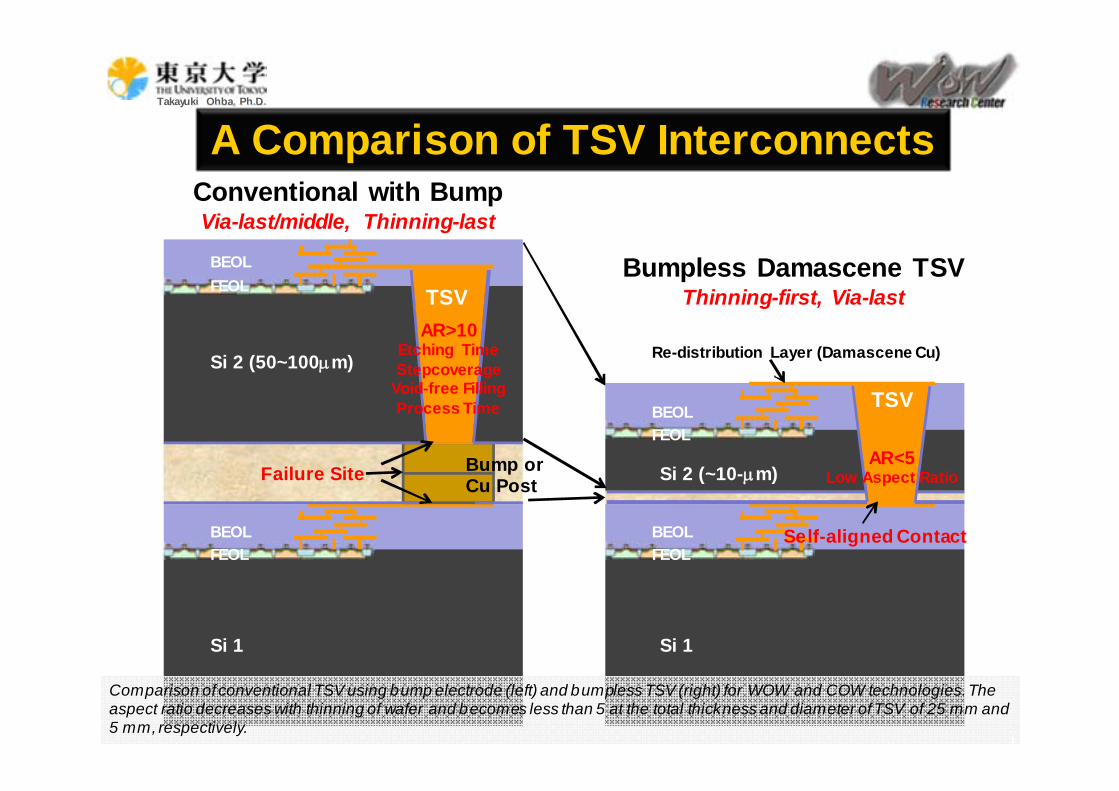
Bumpless Damascene TSVThinning-first, Via-last
AR<5Low Aspect Ratio
Self-aligned Contact
Si 1
BEOLFEOL
BEOLFEOL
Si 2 (~10-m)
TSV
Re-distribution Layer (Damascene Cu)
A Comparison of TSV InterconnectsConventional with BumpVia-last/middle, Thinning-last
BEOLFEOL
AR>10Etching TimeStepcoverage
Void-free FillingProcess Time
Failure Site
Si 2 (50~100m)
Si 1
BEOLFEOL
TSV
Bump orCu Post
Comparison of conventional TSV using bump electrode (left) and bumpless TSV (right) for WOW and COW technologies. The aspect ratio decreases with thinning of wafer and becomes less than 5 at the total thickness and diameter of TSV of 25 mm and5 mm, respectively.
Takayuki Ohba, Ph.D.
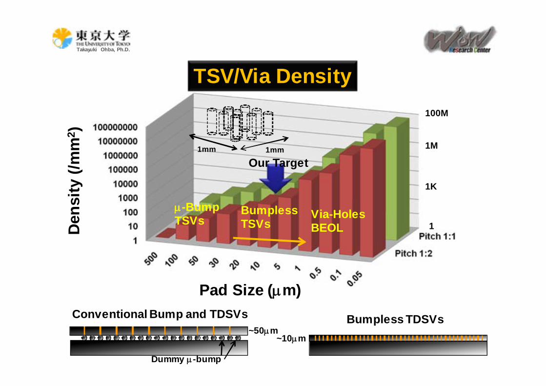
TSV/Via DensityD
ensi
ty (/
mm
2 )
Pad Size (m)
Via-HolesBEOL
BumplessTSVs
-BumpTSVs
100M
1M
1K
1
1mm 1mm
Our Target
Dummy -bump
Conventional Bump and TDSVs Bumpless TDSVs~50m
~10m
Takayuki Ohba, Ph.D.
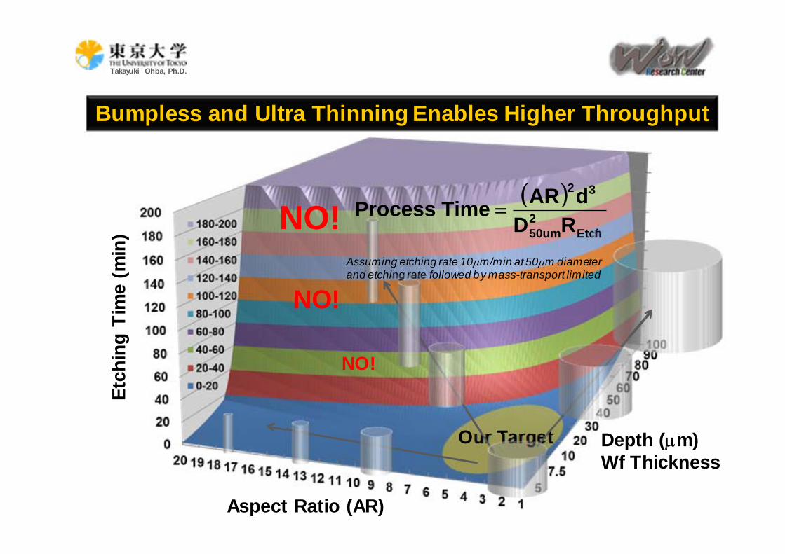
Bumpless and Ultra Thinning Enables Higher ThroughputEt
chin
g Ti
me
(min
)
Aspect Ratio (AR)
Depth (m)Wf Thickness
Our Target
NO!
NO!
NO!
Etch
250um
32
RDdAR Time Process
Assuming etching rate 10m/min at 50m diameter and etching rate followed by mass-transport limited
Takayuki Ohba, Ph.D.
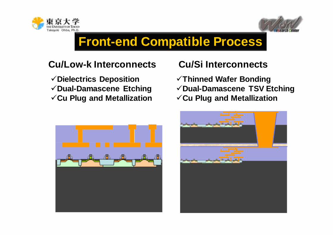
Front-end Compatible Process
Dielectrics DepositionDual-Damascene EtchingCu Plug and Metallization
Thinned Wafer BondingDual-Damascene TSV EtchingCu Plug and Metallization
Cu/Low-k Interconnects Cu/Si Interconnects
Takayuki Ohba, Ph.D.
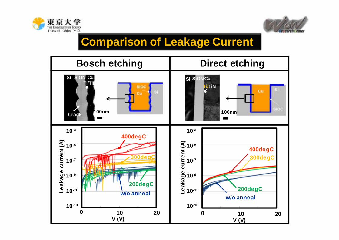
Comparison of Leakage Current
Bosch etching Direct etching
10-13
0 10 20V (V)
Leak
age
curr
ent (
A)
400degC
300degC
200degCw/o anneal10-11
10-9
10-7
10-5
10-3
0 10 20V (V)
Leak
age
curr
ent (
A)
400degC300degC
200degCw/o anneal
10-13
10-11
10-9
10-7
10-5
10-3
100nm
CuSiONSiTi/TiN
100nm
CuSiONSiTi/TiN
Crack
Takayuki Ohba, Ph.D.
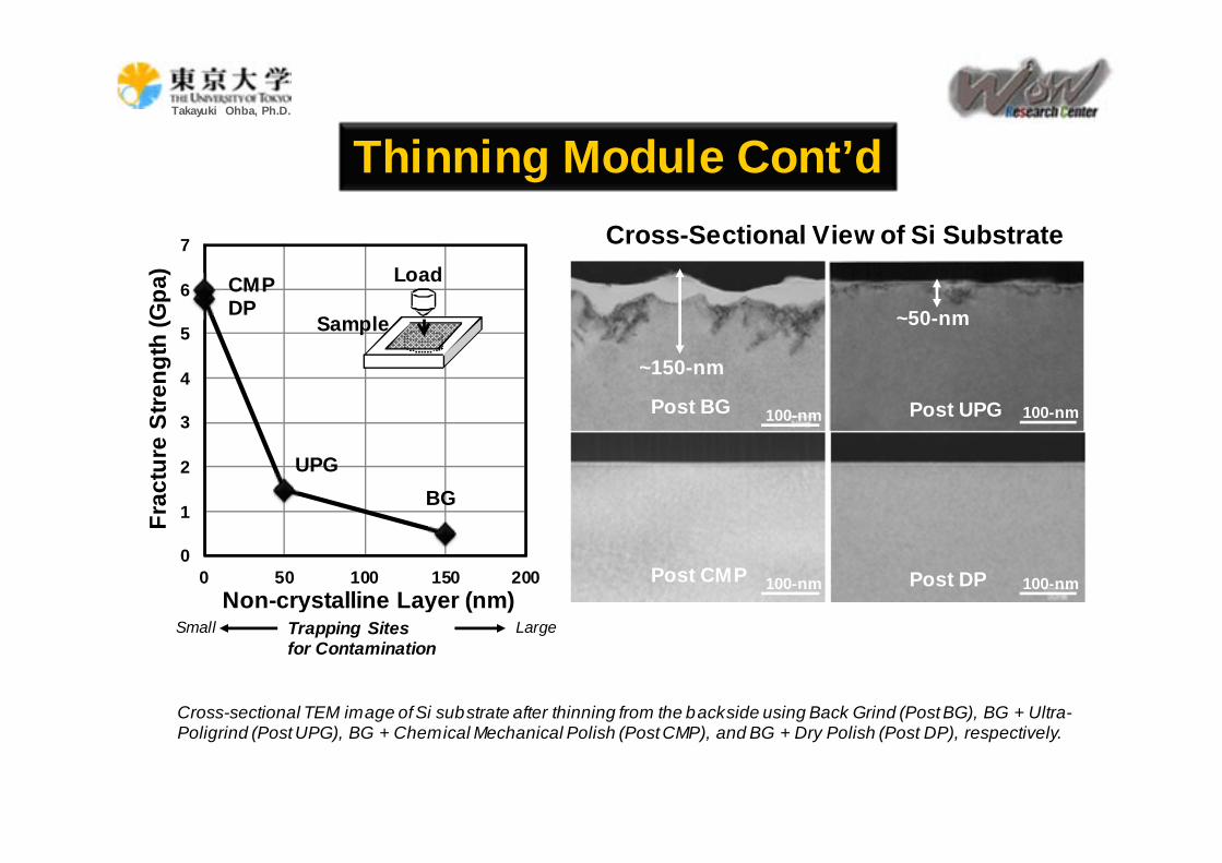
Thinning Module Cont’d
Cross-sectional TEM image of Si substrate after thinning from the backside using Back Grind (Post BG), BG + Ultra-Poligrind (Post UPG), BG + Chemical Mechanical Polish (Post CMP), and BG + Dry Polish (Post DP), respectively.
Post BG 100-nm
~150-nm
100-nmPost UPG
~50-nm
100-nmPost DPPost CMP 100-nm
Cross-Sectional View of Si Substrate
0
1
2
3
4
5
6
7
0 50 100 150 200
Load
Sample
CMPDP
UPGBG
Non-crystalline Layer (nm)
Frac
ture
Stre
ngth
(Gpa
)
Trapping Sitesfor Contamination
LargeSmall
Takayuki Ohba, Ph.D.
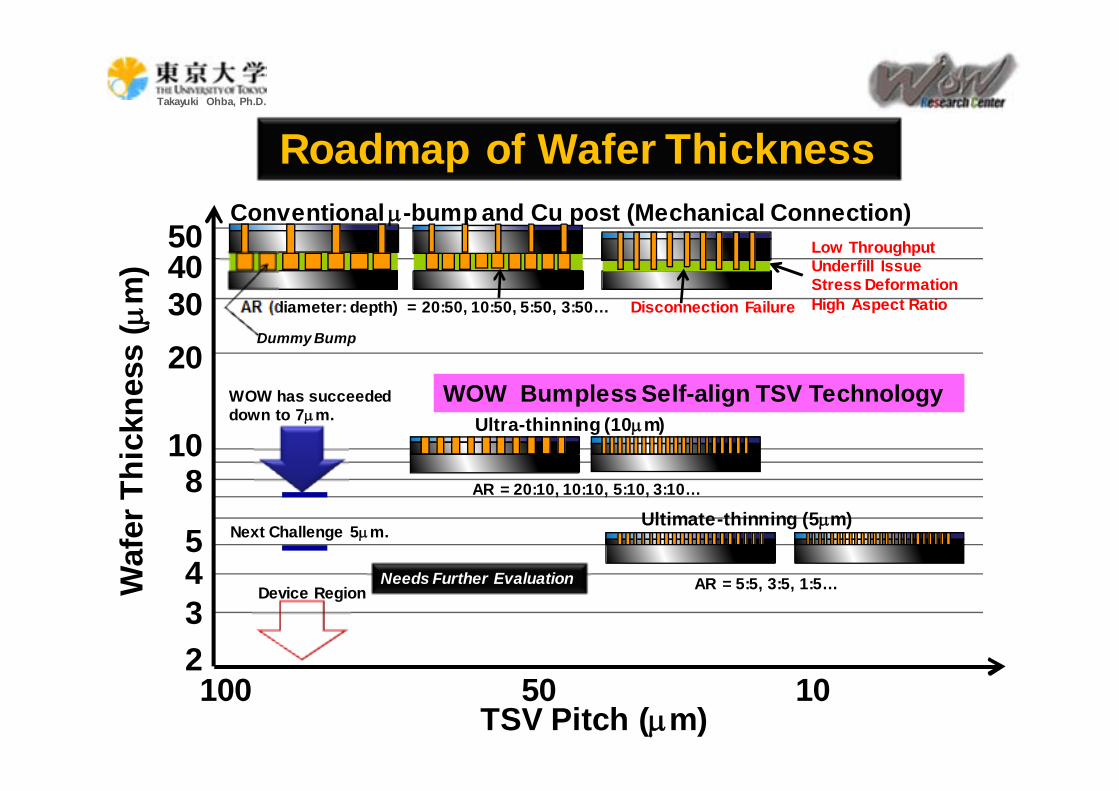
TSV Pitch (m)
Waf
er T
hick
ness
(m
)
5040
20
10
100 50 10
Conventional -bump and Cu post (Mechanical Connection)
AR (diameter: depth) = 20:50, 10:50, 5:50, 3:50… Disconnection Failure
Low Throughput Underfill IssueStress DeformationHigh Aspect Ratio30
8
54
23
WOW Bumpless Self-align TSV Technology
AR = 20:10, 10:10, 5:10, 3:10…
AR = 5:5, 3:5, 1:5…
Ultra-thinning (10m)
Roadmap of Wafer Thickness
WOW has succeeded down to 7m.
Ultimate-thinning (5m)Next Challenge 5m.
Device RegionNeeds Further Evaluation
Dummy Bump
Takayuki Ohba, Ph.D.
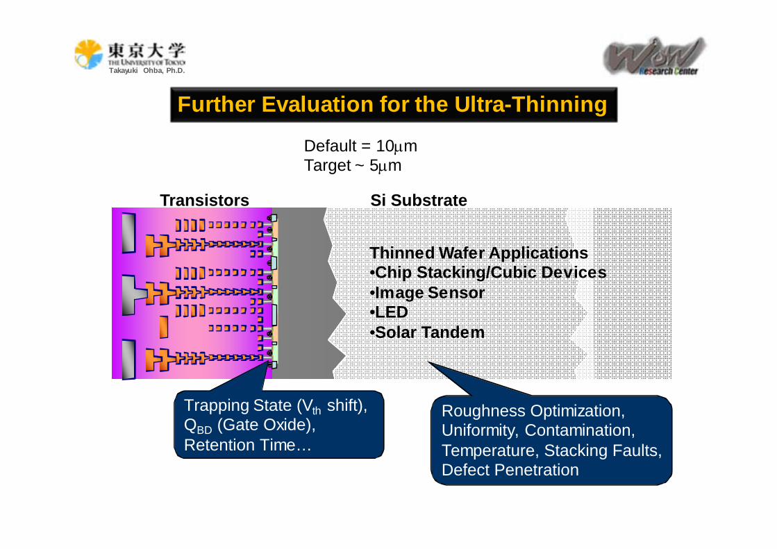
Further Evaluation for the Ultra-Thinning
Transistors
Thinned Wafer Applications•Chip Stacking/Cubic Devices•Image Sensor•LED•Solar Tandem
Default = 10mTarget ~ 5m
Roughness Optimization, Uniformity, Contamination, Temperature, Stacking Faults, Defect Penetration
Trapping State (Vth shift), QBD (Gate Oxide), Retention Time…
Si Substrate
Takayuki Ohba, Ph.D.
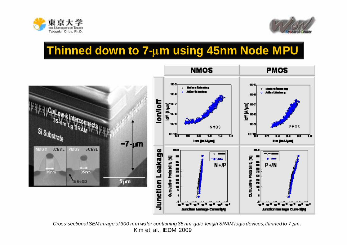
Thinned down to 7-m using 45nm Node MPU
Kim et. al., IEDM 2009Cross-sectional SEM image of 300 mm wafer containing 35 nm-gate-length SRAM logic devices, thinned to 7 m.
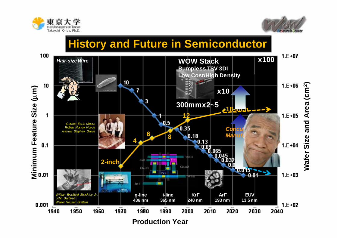
Takayuki Ohba, Ph.D.M
inim
um F
eatu
re S
ize
(m
)
Waf
er S
ize
and
Are
a (c
m2 )
12
864
2-inch
Gordon Earle Moore Robert Norton Noyce
Andrew Stephen Grove
William Bradford Shockley Jr.John BardeenWalter Houser Brattain
History and Future in SemiconductorWOW StackBumpless TSV 3DILow Cost/High Density
18-inch
x100
x10
300mmx2~5
ConcurrentManufacturing
g-line436 nm
i-line365 nm
KrF248 nm
ArF193 nm
EUV13,5 nm
Hair-size Wire
Production Year
Takayuki Ohba, Ph.D.
10-6
10-3
100
103
106
109
1012
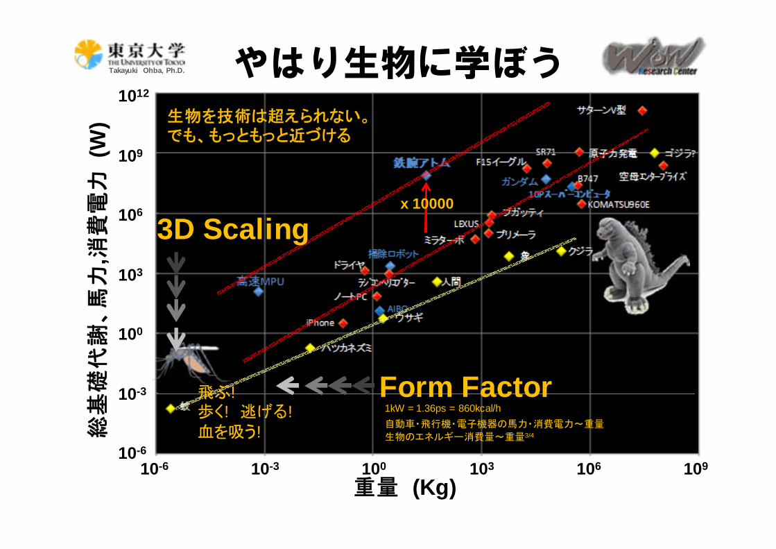
重量 (Kg)
総基
礎代
謝、馬力
,消費電力
(W)
1kW = 1.36ps = 860kcal/h自動車・飛行機・電子機器の馬力・消費電力~重量
生物のエネルギー消費量~重量3/4
10-3 100 103 106 10910-6
x 10000
飛ぶ!歩く! 逃げる!血を吸う!
生物を技術は超えられない。でも、もっともっと近づける
やはり生物に学ぼう
3D Scaling
Form Factor
Takayuki Ohba, Ph.D.
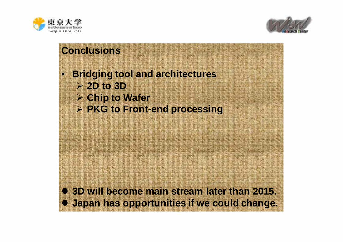
Conclusions
• Bridging tool and architectures 2D to 3D Chip to Wafer PKG to Front-end processing
3D will become main stream later than 2015. Japan has opportunities if we could change.
Takayuki Ohba, Ph.D.
Acknowledgements
This study was carried out based on the three-dimensional integration development program of the WOW Alliance at the University of Tokyo, and the author thanks the more than 20 alliance members, including Nagoya University, ITRI Ad-STAC (Taiwan), and the WOW Research Center Ltd. for their cooperation.
安靜地聽謝謝