Embed Size (px)
Citation preview
Communications Baseband
Project 05500
Preliminary Design Report
February 18, 2005
Sponsor: RIT EE Dept.
Advisors: Dr. Joe DeLorenzo, Dr. Sohail Dianat, Dr. Eli Saber
Team Leader: Leland Smith (EE)
Chief Engineer: Jason Riesbeck (EE)
Electrical Engineer: Jonathan Hutton
Communications Baseband – Project 05500 5/8/2023
Executive Summary
This document provides full detail of the planning and design of the project
Communications Baseband. The name Communications Baseband is actually a misnomer
that originated before the project was redefined by the project leader and advisor Dr. Joe
Delorenzo. Initially this project was to be a base-band signal processing project that
would perform digital signal processing and coding which would then be modulated and
encoded by a Forward Error Correcting project from last year.
This preliminary design report (PDR) is broken down to a system level. Because this
project is three distinct systems that achieve the same goal, this PDR separates each
system as a unique project. Typical design reports break the project down into facets of
the design process from proposal to refinement. However, this project consists of
multiple, unique systems; thus, this PDR is divided by ‘subassembly.’ Each subassembly
refers to an individual, independent, fully functional system. Under each of these
subassemblies, the important design facets are addressed.
First, the background and purpose of the project are discussed. The system definition
and development are then discussed. Subsequently, each subsystem is discussed down to
a component level with the design process being clearly outlined.
Finally, the future of the project is discussed. The tasks that lie ahead and the time
schedule for next quarter are provided.
Preliminary Design Report 2

Communications Baseband – Project 05500 5/8/2023
Table of Contents
EXECUTIVE SUMMARY............................................................................................................................2
TABLE OF CONTENTS...............................................................................................................................3
1 PROJECT PURPOSE AND INTRODUCTION...............................................................................6
1.1 PROJECT MISSION STATEMENT......................................................................................................61.2 BACKGROUND................................................................................................................................61.3 CUSTOMERS...................................................................................................................................71.4 SYSTEM OVERVIEW.......................................................................................................................71.5 CUSTOMER SPECIFICATIONS..........................................................................................................91.6 PROJECT FEASIBILITY..................................................................................................................111.7 DELIVERABLES.............................................................................................................................11
2 SYSTEM CONCEPT DEVELOPMENT.........................................................................................13
2.1 INITIAL SYSTEM PROPOSALS.......................................................................................................132.2 ANALYSIS OF DESIGN PROPOSALS..............................................................................................172.3 DESIGN REFINEMENT...................................................................................................................182.4 SYSTEM FEASIBILITY...................................................................................................................252.5 DEIGN CRITERIA..........................................................................................................................25
3 AUDIO SUBASSEMBLY..................................................................................................................27
3.1 SUBSYSTEM INTRODUCTION........................................................................................................273.2 CONCEPT DEVELOPMENT.............................................................................................................283.3 FEASIBILITY ASSESSMENT...........................................................................................................293.4 DESIGN OBJECTIVES....................................................................................................................293.5 DESIGN SYNTHESIS......................................................................................................................313.6 PRELIMINARY SYSTEM DEFINITION.............................................................................................37
4 AM SUBASSEMBLY.........................................................................................................................39
4.1 SUBSYSTEM INTRODUCTION........................................................................................................394.2 CONCEPT DEVELOPMENT.............................................................................................................404.3 FEASIBILITY ASSESSMENT...........................................................................................................434.4 DESIGN OBJECTIVES....................................................................................................................444.5 DESIGN SYNTHESIS......................................................................................................................464.6 PRELIMINARY SYSTEM DEFINITIONS...........................................................................................50
5 FM SUBASSEMBLIES......................................................................................................................54
5.1 CONCEPTUAL DESIGN..................................................................................................................545.2 PRELIMINARY FEASIBILITY ASSESSMENT....................................................................................555.3 CONCEPT DEVELOPMENT.............................................................................................................565.4 FEASIBILITY ASSESSMENT...........................................................................................................575.5 TARGET SPECIFICATIONS.............................................................................................................585.6 DESIGN SYNTHESIS......................................................................................................................595.7 DESIGN DOCUMENTS...................................................................................................................59
6 FSK SUBASSEMBLY........................................................................................................................60
6.1 PRELIMINARY FEASIBILITY ASSESSMENT....................................................................................606.2 CONCEPT DEVELOPMENT.............................................................................................................606.3 FEASIBILITY ASSESSMENT...........................................................................................................626.4 TARGET SPECIFICATIONS.............................................................................................................626.5 DESIGN SYNTHESIS......................................................................................................................636.6 DESIGN DOCUMENTS...................................................................................................................63
Preliminary Design Report 3
Communications Baseband – Project 05500 5/8/2023
7 DIGITAL PROCESSING AND CONTROL SUBSYSTEM..........................................................64
7.1 SUBSYSTEM INTRODUCTION........................................................................................................647.2 CONCEPT DEVELOPMENT.............................................................................................................657.3 FEASIBILITY ASSESSMENT...........................................................................................................737.4 DESIGN OBJECTIVES....................................................................................................................747.5 DESIGN SYNTHESIS......................................................................................................................777.6 PRELIMINARY SYSTEM DEFINITION.............................................................................................82
8 CURRENT DESIGN..........................................................................................................................85
8.1 SYSTEM DEFINITION....................................................................................................................858.2 TARGET SYSTEM SPECIFICATIONS...............................................................................................868.3 PRELIMINARY BUDGET ANALYSIS...............................................................................................87
9 PROJECT OUTLOOK......................................................................................................................88
9.1 SENIOR DESIGN I – WINTER QUARTER.......................................................................................889.2 SENIOR DESIGN II - SPRING QUARTER........................................................................................929.3 BEYOND SDII..............................................................................................................................94
APPENDIX A – REFERENCES.................................................................................................................95
APPENDIX B – DESIGN DOCUMENTS.................................................................................................96
CHOOSING A DAC.....................................................................................................................................97LOGARITHMIC AMPLIFIER..........................................................................................................................99PICMICRO MICROCONTROLLER SPECIFICATIONS....................................................................................100A/D CONVERSION AND THE PICMICRO CRYSTAL OSCILLATOR..............................................................104FM TRANSMITTER SCHEMATIC................................................................................................................107PARTS LIST – FM TRANSMITTER............................................................................................................108INTERCONNECTION CONTROL DOCUMENT - FM TRANSMITTER BOARD.................................................109FM RECEIVER SCHEMATIC......................................................................................................................110PARTS LIST – FM RECEIVER....................................................................................................................111INTERCONNECTION CONTROL DOCUMENT - FM RECEIVER BOARD.......................................................112FM RECEIVER SCHEMATIC......................................................................................................................113PARTS LIST – FSK TRANSCEIVER............................................................................................................114INTERCONNECTION CONTROL DOCUMENT - GFSK BOARD....................................................................115GFSK BOARD PROTOCOL GUIDELINES...................................................................................................116GFSK CONTROL WORD...........................................................................................................................119FURTHER LOOK INTO ISM BAND REGULATIONS.....................................................................................120Choosing Capacitors................................................................................................................................121
Preliminary Design Report 4

Communications Baseband – Project 05500 5/8/2023
List of Figures
Figure 1 - Organizational Work Chart.................................................................................8Figure 2 – Concept #1 Universal AM/FM/ASK/FSK System..........................................12Figure 3 – Concept #2 Analog Voice and Wireless RS232...............................................13Figure 4 – Concept #3 Wireless USB................................................................................14Figure 5 – Concept #4 Analog Voice and Streaming Audio.............................................15Figure 6 – Subsystems Block Diagram.............................................................................18Figure 7 Basic Block Diagram of Transmitter Side Audio Subsystem.............................26Figure 8: Basic Block Diagram of Receiver Side Audio Subsystem................................26Figure 9: Filter Representation..........................................................................................27Figure 10: Op-Amp in Gain Formation.............................................................................31Figure 11: 1st Iteration LPF Schematic.............................................................................33Figure 12: 1st Iteration LPF Frequency Response............................................................33Figure 13: 2nd Iteration LPF Schematic............................................................................34Figure 14: 2nd Iteration LPF Frequency Response...........................................................34Figure 15: Audio Subsystem Circuit Diagram..................................................................36Figure 16: Basic Block Diagram of AM Transmit Subsystem..........................................38Figure 17: Basic Block Diagram of AM Receive Subsystem...........................................38Figure 18: Envelope Detector............................................................................................42Figure 19: Clock Oscillator and RLC Filter......................................................................46Figure 20: Clock Oscillator and Buffer Amplifier............................................................50Figure 21: Audio Input Buffer...........................................................................................50Figure 22: Mixer, RF Amplifier, and Antenna..................................................................51Figure 23: Antenna and AM Receiver...............................................................................51Figure 24 – Frequency Modulation of a Carrier................................................................53Figure 25 – Basic FM Transmitter.....................................................................................54Figure 26 – Basic Superheterodyne FM Receiver.............................................................54Figure 27 – Digital Processing and Control Subsystem Block Diagram...........................62Figure 28 - Spectrum of original signal.............................................................................65Figure 29 - Frequency Spectrum of Sampled Signal.........................................................65Figure 30 - Quantization of an analog signal into L levels................................................66Figure 31 - PIC Transmit Side Program Flow Chart.........................................................74Figure 32 - Receive side PIC program flow chart.............................................................75Figure 33 - Timing Diagram for FSK Chip in Shockburst Mode......................................78Figure 34 - Asynchronous Data Transmission – 2 Samples..............................................79Figure 35 - Asynchronous Data Transmission - 1 Sample................................................79Figure 36 - Transmit Side Pin to Pin PIC-FSK Connections............................................81Figure 37 - Receiver Side Pin to Pin PIC-FSK-DAC Connections...................................81Figure 38 – Current System Block Diagram.....................................................................83
Preliminary Design Report 5

Communications Baseband – Project 05500 5/8/2023
1 Project Purpose and IntroductionThis section will introduce the project goals, purpose, and history. The customers
will be acknowledged and their specifications delineated. A system overview and
diagrams will be given. Finally the project timeline and deliverables will be proposed.
1.1 Project Mission StatementThe goal is to have a communications system consisting of a modulator and
demodulator such that three methods of modulation are employed on an analog signal
(namely AM, FM, and PCM). To be sure the project is completed by Senior Design II,
only analog input signals (e.g. music or voice) will be considered for the system. If the
analog transmission is successfully completed early, the capability of transmitting serial
data from an external source will be added.
The system will wirelessly transmit the modulated signal a classrooms length to a
demodulator. The demodulator will perform the reverse process and output the analog
voice signal to a speaker. The system will allow for a spectrum analyzer and other lab
equipment to easily connect to it for viewing the spectrum of the modulated signal.
1.2 BackgroundThis project was initiated in a cumulative effort of professors in the RIT electrical
engineering department to provide interactive laboratory equipment that would
demonstrate the application of communications theory. The implementation of several
modulation techniques will support a corresponding class in communications theory. The
desire was to have a system such that different methods of modulation are employed on
an input signal. This will be used to show students useful information such as the
frequency spectrum of each modulated signal.
Preliminary Design Report 6
Communications Baseband – Project 05500 5/8/2023
1.3 CustomersThe customers for this project are Dr. Joe Delorenzo, Dr. Eli Saber, and Dr. Sohail
Dianat. They are all professors at Rochester Institute of Technology and teach the
communications courses for undergraduate and graduate level. Ultimately the RIT
electrical engineering department is the end customer since this project will be used for
the undergraduate communications class. The RIT EE department is the sponsor for the
cost of materials as well.
1.4 System OverviewThis system will implement three types of modulation on an analog input. The
project can be broken into major functions that must be performed. Each of these
functions is found in the systems as defined in Chapter 2 and described in detail in the
rest of the document. These main system functions are outlined as follows:
1) Analog Input (Source)
2) Analog Processing
3) Amplitude Modulation/Demodulation
4) Frequency Modulation/Demodulation
5) Analog to Digital Conversion (PCM)
6) Frequency Shift Keying (FSK modulation/demodulation)
7) Digital to Analog Conversion
8) Analog Output (Sink)
The analog input in our project will be a standard vocal microphone. Also line level
audio may be plugged in from any audio source (e.g. compact disk player, MP3 player,
etc.). Analog processing will modify the analog signal so that it is suitable for digital
conversion and modulation. The signal will be amplified and then passed through a low
Preliminary Design Report 7
Communications Baseband – Project 05500 5/8/2023
pass filter to attenuate any unwanted frequencies. This will be necessary to prevent
aliasing when the analog signal is sampled. These things are all part of the audio
subassembly and are subsequently discussed in Chapter 3.
Amplitude modulation and demodulation will be performed on the analog signal as
a separate system. This is discussed in detail in Chapter 4. Frequency modulation is also
its own system that modulates the analog audio as discussed in Chapter 5.
Analog to digital conversion will be used to implement base-band pulse code
modulation. This is part of the digital processing and control subsystem discussed in
Chapter 7.
Frequency Shift Keying is the method of modulation used to wirelessly transmit the
binary PCM signal stream. This is fully discussed in Chapter 6.
Digital to analog conversion is part of the audio processing discussed in Chapter 7.
Finally the received analog signal must be conveyed to show that successful
demodulation has occurred. In this project, only audio signals are used therefore the
output will be a speaker for human hearing of the transmitted signal.
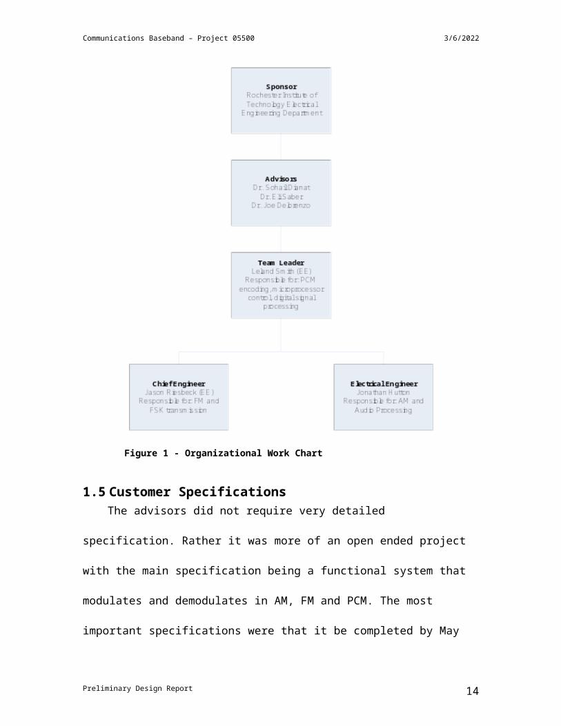
1.4.1 Project Organizational ChartThe following chart in Figure 1 shows the organizational chart of the project.
Preliminary Design Report 8
Communications Baseband – Project 05500 5/8/2023
Figure 1 - Organizational Work Chart
1.5 Customer SpecificationsThe advisors did not require very detailed specification. Rather it was more of an
open ended project with the main specification being a functional system that modulates
and demodulates in AM, FM and PCM. The most important specifications were that it be
completed by May and be suitable for using in the classroom as a demonstration tool.
Any additional time we may have may be used to add additional functionality to the
project.
Preliminary Design Report 9
Communications Baseband – Project 05500 5/8/2023
The minimum specifications for the project were defined by the advisors and are
delineated here.
The input signal should be from a microphone or some other analog device.
The bandwidth or range of the input analog signals should be at least voice
quality audio.
The modulation methods employed should be AM (amplitude modulation), FM
(frequency modulation), and PCM (pulse code modulation) version of the input.
There should be some means of viewing the spectrum of the modulated signal
on a spectrum analyzer.
The project should be wireless with a minimal range of a room size.
A suitable receiver should demodulate the signal and send it to an appropriate
sink (e.g. a speaker or computer for digital) so there is some way of knowing the
signal was successfully received.
The project should consist of two self-contained modules that provide
modulation of the analog signal and demodulation of the transmitted signal.
All circuitry and components necessary to complete these two operations should
be contained in some solid container allowing visibility of the components and
portability of the unit.
An external microphone should be provided and the necessary input jacks
mounted to the transmit module.
The receive module should have a mounted speaker and any necessary output
ports to access the demodulated signal.
Antennas should be mounted to the module.
Preliminary Design Report 10
Communications Baseband – Project 05500 5/8/2023
Each module should have appropriate labeling of all peripherals.
Each module should have control switches to select which modulation scheme
is to be used.
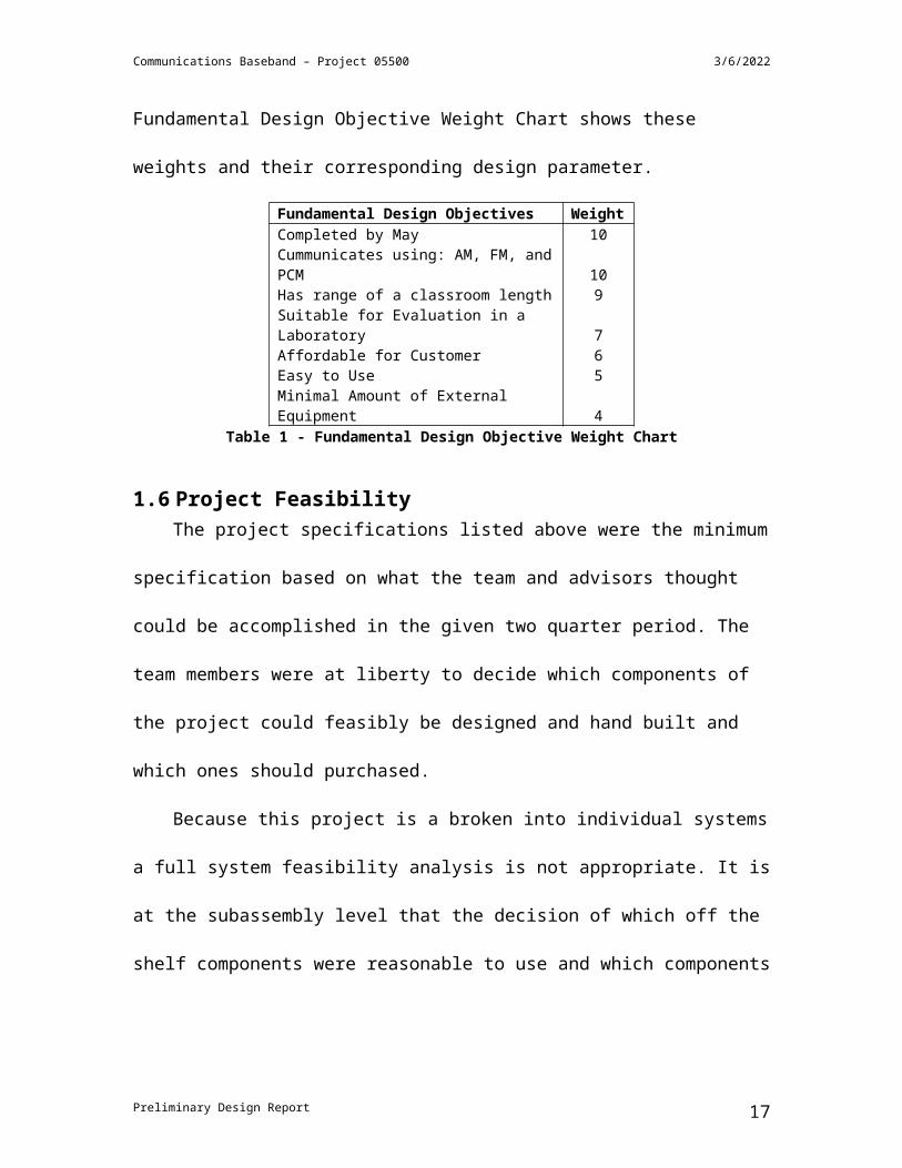
The fundamental design objectives were weighted to show which design parameters
are most important. Table 1 - Fundamental Design Objective Weight Chart shows these
weights and their corresponding design parameter.
Fundamental Design Objectives WeightCompleted by May 10Cummunicates using: AM, FM, and PCM 10Has range of a classroom length 9Suitable for Evaluation in a Laboratory 7Affordable for Customer 6Easy to Use 5Minimal Amount of External Equipment 4Table 1 - Fundamental Design Objective Weight Chart
1.6 Project FeasibilityThe project specifications listed above were the minimum specification based on
what the team and advisors thought could be accomplished in the given two quarter
period. The team members were at liberty to decide which components of the project
could feasibly be designed and hand built and which ones should purchased.
Because this project is a broken into individual systems a full system feasibility
analysis is not appropriate. It is at the subassembly level that the decision of which off the
shelf components were reasonable to use and which components were feasible to design.
Thus the feasibility is discussed for each subassembly.
1.7 DeliverablesThe Communications Baseband team shall provide the following to our customers
and RIT EE department at the end of the two quarter series of Senior Design I and II,
May 2005:
Preliminary Design Report 11
Communications Baseband – Project 05500 5/8/2023
1 Transmit module capable of modulating an analog input using AM, FM and
PCM.
1 Receiver module capable of demodulating the transmitted signal in either AM,
FM, or PCM.
Operator Manual with complete I/O specifications for each board and each
module, operation instructions, conditions of operation, and any other
appropriate information regarding the use of the system.
Critical Design Report: A final report that contains detailed documentation of
the design process of the system, final diagrams detailing the module and
subsystem signal flow, calculations and mathematical derivations, variations in
operation from specifications (if any), implementation caveats, simulation
results and source codes, summary of test results, known issues or problems,
and final conclusions.
Preliminary Design Report 12
Communications Baseband – Project 05500 5/8/2023
2 System Concept DevelopmentThis section develops the project at a system level. A design process is used to
narrow in on a final design after brain storming. Then the selected system is broken into
subsystems, and specific task are designated for each.
2.1 Initial System Proposals The team proposed a variety of system architectures. In this section the pilot
systems will be introduced. Each idea will be discussed and analyzed. Ultimately,
impracticable designs will be dismissed for reasons of unfeasibility or unmet design
objectives and a final system design will be reached.
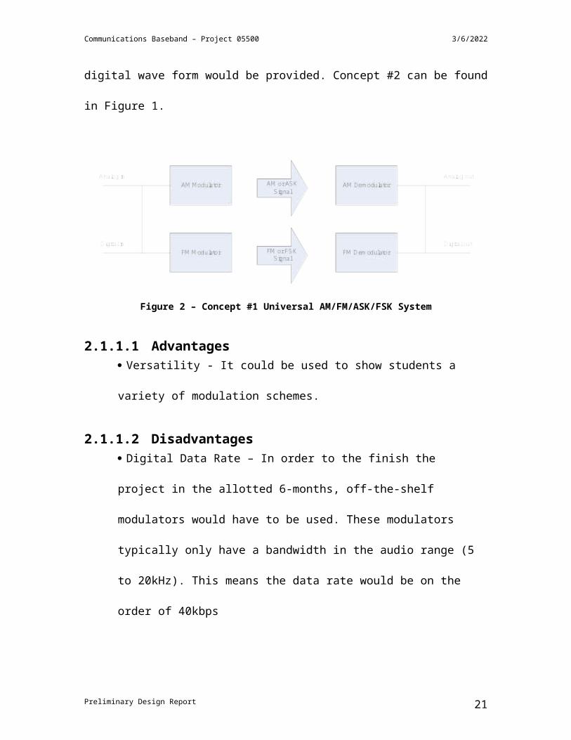
2.1.1 Concept #1 Universal AM/FM/ASK/FSKThe first idea was to create a universal transmitter/receiver that could transmit
analog AM, analog FM, ASK, and FSK. The AM and FM modulators would be of typical
architecture and would provide enough bandwidth for digital transmission. To transmit
analog an audio signal would be placed on the modulator. To transmit digital a digital
wave form would be provided. Concept #2 can be found in Figure 1.
Figure 2 – Concept #1 Universal AM/FM/ASK/FSK System
Preliminary Design Report 13
Communications Baseband – Project 05500 5/8/2023
2.1.1.1 Advantages Versatility - It could be used to show students a variety of modulation schemes.
2.1.1.2 Disadvantages Digital Data Rate – In order to the finish the project in the allotted 6-months,
off-the-shelf modulators would have to be used. These modulators typically only
have a bandwidth in the audio range (5 to 20kHz). This means the data rate would
be on the order of 40kbps
Usefulness – The question is still asked “what will the digital portion be used
for?” The operator would have to provide a digital signal for demonstration. The
point of the digital portion seems moot without some sort of device to facilitate
the transmission of useful digital data.
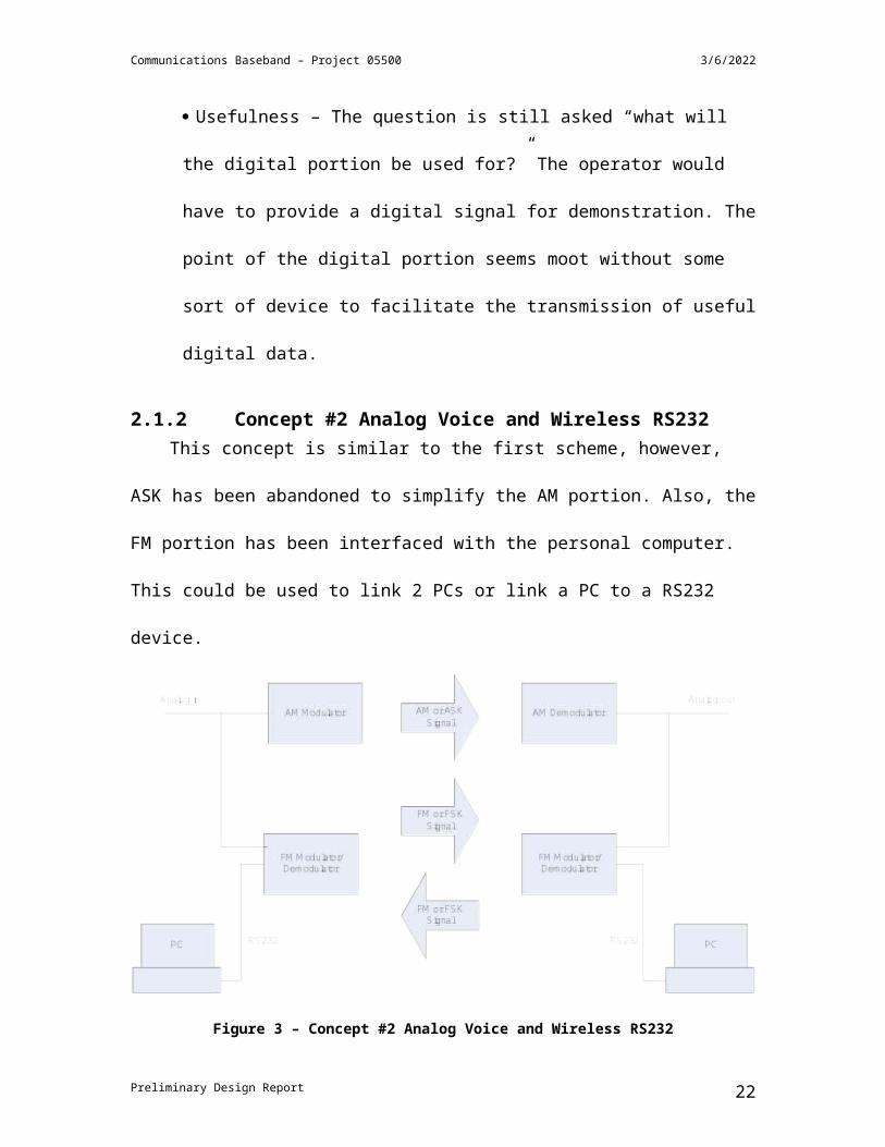
2.1.2 Concept #2 Analog Voice and Wireless RS232 This concept is similar to the first scheme, however, ASK has been abandoned to
simplify the AM portion. Also, the FM portion has been interfaced with the personal
computer. This could be used to link 2 PCs or link a PC to a RS232 device.
Preliminary Design Report 14

Communications Baseband – Project 05500 5/8/2023
Figure 3 – Concept #2 Analog Voice and Wireless RS232
2.1.2.1 Advantages Reasonable Bandwidth – Data rates for RS232 are low (20kbps (1b)) making it
suitable for an analog channel.
2.1.2.2 Disadvantages Requires Two Way Communication – This will complicate the design slightly.
Not Particularly a PCM Solution – This solution is still only an audio channel
that is to be used to transmit digital data. It may be more useful and educational to
have a dedicated digital transmitter.
Requires Extra Lab Equipment – This setup requires the availability of at least
one computer which conflicts with the design objectives.
2.1.3 Concept #3 Analog Voice and Wireless USBThis concept is similar to concept number 2, however, it implements a separate
module for PCM transmission and supports wireless USB. Analog AM and FM are also
implemented (though not shown in Figure 4).
Figure 4 – Concept #3 Wireless USB
2.1.3.1 Advantages Impressive Bandwidth – USB operates at 1.5 to 480Mbps. Sending data at this
speed would be a great achievement.
Preliminary Design Report 15
Communications Baseband – Project 05500 5/8/2023
2.1.3.2 Disadvantages Difficult to Implement – Bit rates of over 1Mbps require high carrier
frequencies often in the Ghz range. Extra care is necessary when building a
system for Ghz operation. High band width systems also have more noise
problems because noise power is passed through the wide front end filter.
Requires Two Way Communication – This will complicate the design slightly.
Requires Extra Lab Equipment – This setup requires the availability of at least
one computer which conflicts with the design objectives.
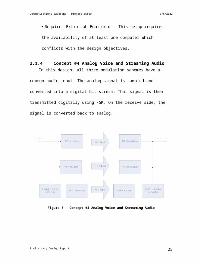
2.1.4 Concept #4 Analog Voice and Streaming AudioIn this design, all three modulation schemes have a common audio input. The
analog signal is sampled and converted into a digital bit stream. That signal is then
transmitted digitally using FSK. On the receive side, the signal is converted back to
analog.
Figure 5 – Concept #4 Analog Voice and Streaming Audio
Preliminary Design Report 16
Communications Baseband – Project 05500 5/8/2023
2.1.4.1 Advantages Comparison of modulation schemes – All three modulation schemes can be
compared directly because this architecture uses a single audio source. This setup
is ideal for demonstrating the tradeoffs of all three sections.
No external equipment – A demonstration can be performed without an external
signal source.
One Way Communication – This simplifies the design. The setup can easily be
converted to dual directional if an extra set of modulators and demodulators are
produced.
2.1.4.2 DisadvantagesThere are no obvious disadvantages at this time. One concern is the bandwidth
required for uncompressed streaming audio. This figure will be a product of the sample
size and the sampling frequency chosen. Thus allowing a few degrees of freedom. Once
an analysis of the system is performed, a sample size and rate can be chosen based on the
hardware limitations.
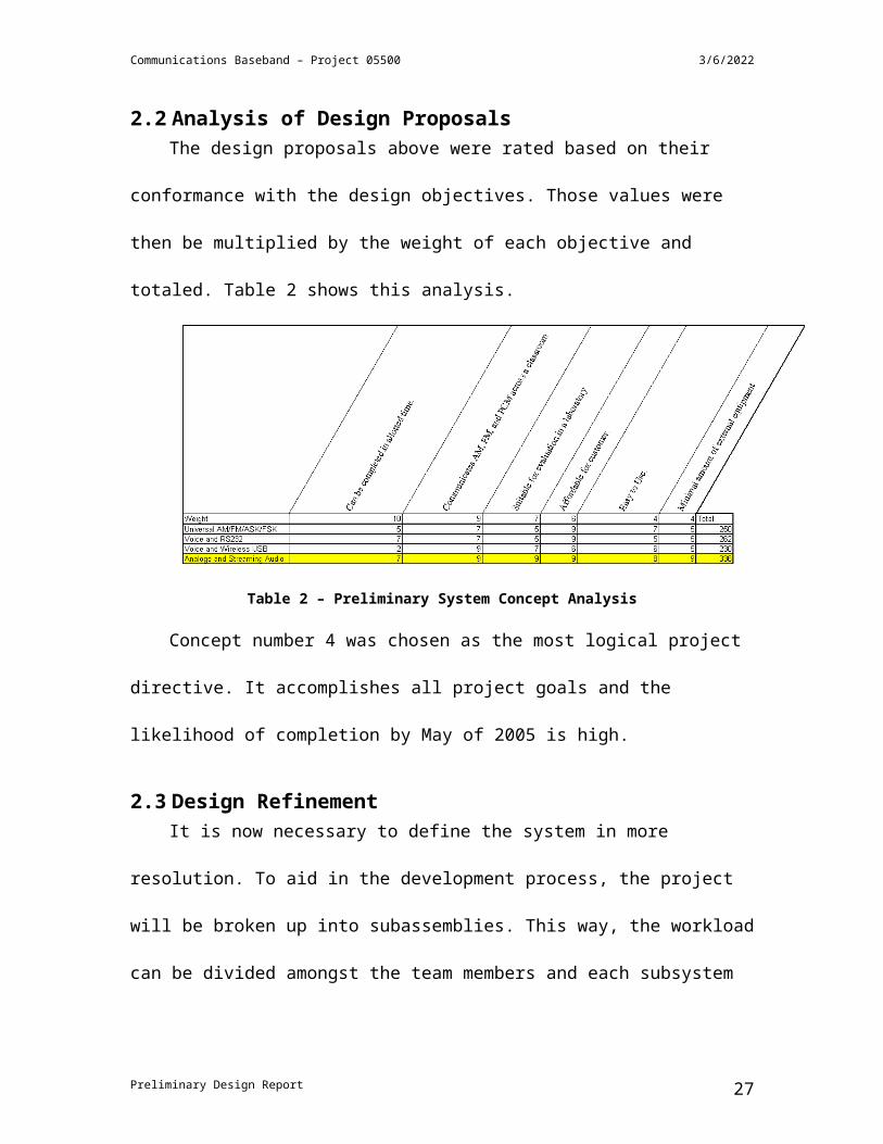
2.2 Analysis of Design ProposalsThe design proposals above were rated based on their conformance with the design
objectives. Those values were then be multiplied by the weight of each objective and
totaled. Table 2 shows this analysis.
Preliminary Design Report 17
Communications Baseband – Project 05500 5/8/2023
Table 2 – Preliminary System Concept Analysis
Concept number 4 was chosen as the most logical project directive. It accomplishes
all project goals and the likelihood of completion by May of 2005 is high.
2.3 Design RefinementIt is now necessary to define the system in more resolution. To aid in the
development process, the project will be broken up into subassemblies. This way, the
workload can be divided amongst the team members and each subsystem can be
developed independently. Performance and interconnection specifications will be
developed for each.
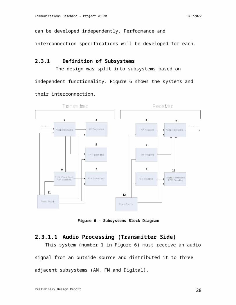
2.3.1 Definition of SubsystemsThe design was split into subsystems based on independent functionality.
Figure 6 shows the systems and their interconnection.
Preliminary Design Report 18
Communications Baseband – Project 05500 5/8/2023
Figure 6 – Subsystems Block Diagram
2.3.1.1 Audio Processing (Transmitter Side)This system (number 1 in Figure 6) must receive an audio signal from an outside
source and distributed it to three adjacent subsystems (AM, FM and Digital).
Input – Input must be in the form of radiated vocals from a human speaking at a
nominal volume. Unit must have adjustable gain to facilitate a human speaking at a
range of volume levels. These specific levels must be characterized by the designer of the
subsystem.
Additional inputs can be added such as a line level RCA input from a stereo or
walkman. These addition inputs should only be pursued after the primary input (above)
has been satisfied.
Preliminary Design Report 19
Communications Baseband – Project 05500 5/8/2023
Output – Three line level audio outputs must be supplied to adjacent subsystems.
These outputs must be adjustable or easily adaptable for connection to a range of
subsystems.
Power Consumption and Supply Voltage – This system must operate from a
signal supply voltage of 9V DC.
2.3.1.2 Audio Processing (Receiver Side)This system (number 2 in Figure 6) must receive an audio signal from the three
adjacent subsystems (AM, FM and Digital) and broadcast it from a speaker.
Input – Three line level audio inputs will be supplied from adjacent subsystems.
These inputs must be adjustable or easily adaptable for connection to a range of
subsystems.
Output – Input must be in the form of radiated audio. This sound must be audible by
a typical human in a typical classroom with a typical amount of ambient noise. These
specific audio levels must be characterized by the designer of the subsystem.
Additional outputs can be added such as a line level RCA output for a stereo or
recording device. These addition inputs should only be pursued after the primary output
(above) has been satisfied.
Power Consumption and Supply Voltage – This system must operate from a
signal supply voltage of 9V DC.
2.3.1.3 AM Transmitter This system (number 3 in Figure 6) must receive an audio signal from the audio
board and electromagnetically broadcast it using AM.
Input – The system must be capable of receiving a signal level audio signal
Preliminary Design Report 20
Communications Baseband – Project 05500 5/8/2023
Output – Output must be an AM signal. This system should be designed in
conjunction with the AM receiver. It is the responsibility of the designer to characterize
the AM signal and determine the signal strength necessary to maintain a wireless link
over a distance equal to the length of a classroom.
Power Consumption and Supply Voltage – This system must operate from a
signal supply voltage of 9V DC.
2.3.1.4 AM ReceiverThis system (number 4 in Figure 6) must receive an electromagnetically radiated
AM and supply a demodulated audio signal to the audio board.
Input – Input must be an AM modulated signal. This system should be designed in
conjunction with the AM Transmitter. It is the responsibility of the designer to
characterize the AM signal and determine the receiver sensitivity necessary to maintain a
wireless link over a distance equal to the length of a classroom.
Output – The system must be capable of delivering a signal level audio signal
Power Consumption and Supply Voltage – This system must operate from a signal
supply voltage of 9V DC.
2.3.1.5 FM Transmitter This system (number 5 in Figure 6) must receive an audio signal from the audio
board and electromagnetically broadcast it using FM.
Input –The system must be capable of receiving a signal level audio signal.
Output – Output must be an FM signal. This system should be designed in
conjunction with the FM receiver. It is the responsibility of the designer to characterize
Preliminary Design Report 21
Communications Baseband – Project 05500 5/8/2023
the FM signal and determine the signal strength necessary to maintain a wireless link
over a distance equal to the length of a classroom.
Power Consumption and Supply Voltage – This system must operate from a
signal supply voltage of 9V DC while consuming no more than 100mA of current.
2.3.1.6 FM ReceiverThis system (number 6 in Figure 6) must receive an electromagnetically radiated
FM signal and supply a demodulated audio signal to the audio board.
Input – Input must be an FM modulated signal. This system should be designed in
conjunction with the FM Transmitter. It is the responsibility of the designer to
characterize the FM signal and determine the receiver sensitivity necessary to maintain a
wireless link over a distance equal to the length of a classroom.
Output – The system must deliver a line level audio signal.
Power Consumption and Supply Voltage – This system must operate from a
signal supply voltage of 9V DC.
2.3.1.7 FSK Transmitter This system (number 7 in Figure 6) must receive a digital bit stream from the digital
board and transmit it using FSK.
Bit Rate – Bit rate should be high enough to facilitate uncompressed streaming
audio. It is the responsibility of the system designer to provide the highest bit rate
possible in a design that can be completed in the allotted time.
Digital I/O – Control and data transfer to the FSK board should be conducted
through no more than 10 digital control lines. During development, a high level of
Preliminary Design Report 22
Communications Baseband – Project 05500 5/8/2023
communication should be maintained between the developers of the FSK and digital
control systems. This is recommended to elevate any problems with compatibility.
Output – Output must be an FSK signal. This system should be designed in
conjunction with the FSK receiver. The system designer should perform all necessary
calculations to be sure that the transmitter and receiver are compatible. Also, signal
strength should be strong enough to maintain a wireless link over a distance equal to the
length of a classroom.
Power Consumption and Supply Voltage – This system must operate from a
signal supply voltage of 9V DC.
2.3.1.8 FSK ReceiverThis system (number 8 in Figure 6) must receive an electromagnetically radiated
FSK signal and deliver it to the digital board.
Requirements for digital I/O and bit rate are the same as described in Section
(2.3.1.7.) The main requirement is that the receiver is compatible with the transmitter.
2.3.1.9 Digital Control and PCM Encoding (Transmitter Side)This system (number 9 in Figure 6) should supply the FSK board with a digital
representation of the supplied audio signal. The Digital board will also supply the FSK
board with any control that is required.
Input – The system must be capable of receiving a line level audio signal.
Digital I/O – The digital board must supply the FSK board with a digital
representation of the analog input. Proper formatting must be done to facilitate
transmission via a wireless link. The digital portion must also provide the FSK board
Preliminary Design Report 23

Communications Baseband – Project 05500 5/8/2023
with the proper control information. The designer must work with the designer of the
FSK portion to make sure all requirements are met.
Power Consumption and Supply Voltage – This system must operate from a signal
supply voltage of 9V DC while consuming no more than 100mA of current.
2.3.1.10 Digital Control and PCM Encoding (Receiver Side)This system (number 10 in Figure 6) should retrieve data from the FSK receiver and
transform it back into an audio signal. The Digital board will also supply the FSK board
with any control that is required.
Output - The system must supply the audio board with a line level audio signal.
Digital I/O –The digital portion must provide the FSK board with the proper control
information. Also, the designer must work with the designer of the FSK portion to make
sure that the two boards can communicate with each other.
Power Consumption and Supply Voltage – This system must operate from a signal
supply voltage of 9V DC.
2.3.1.11 Power SuppliesThese systems (numbers 11 and 12 in Figure 6) will provide power to all of the
subsystems. To avoid cross contamination of power supply noise between systems, both
supplies on the receiving and transmitting side will provide a single voltage of 9VDC.
Each subsystem will be responsible for regulating the voltage down to the necessary
levels. Each of these regulators will provide isolation from the 9V supply and thus will
prevent noise contamination. Another reason to have one regulator per subsystem is to
prevent noise from the wring harness. Noise picked up in the wiring harness will be
filtered out by the regulators.
Preliminary Design Report 24
Communications Baseband – Project 05500 5/8/2023
The power supply unit should be comprised of off-the-shelf batteries or a 120VAC
to 9DC power supply.
2.4 System FeasibilityThe development of this system has revolved around the idea that feasibility
should be assessed at a subsystem level. If the design responsibilities and criteria are met,
system integration should be straight forward. The engineers of each subsystem have the
ability to tailor system architecture and minor performance specifications in the name of
product achievability. Therefore, a system level feasibility assessment is not necessary. If
it is found that one of the subsystems is not feasible, this estimation can be revisited.
2.5 Deign CriteriaMost of the system level design specifications have been defined in the above
sections. The fundamental standard is that individual designs adhere to the subsystem
definitions above.
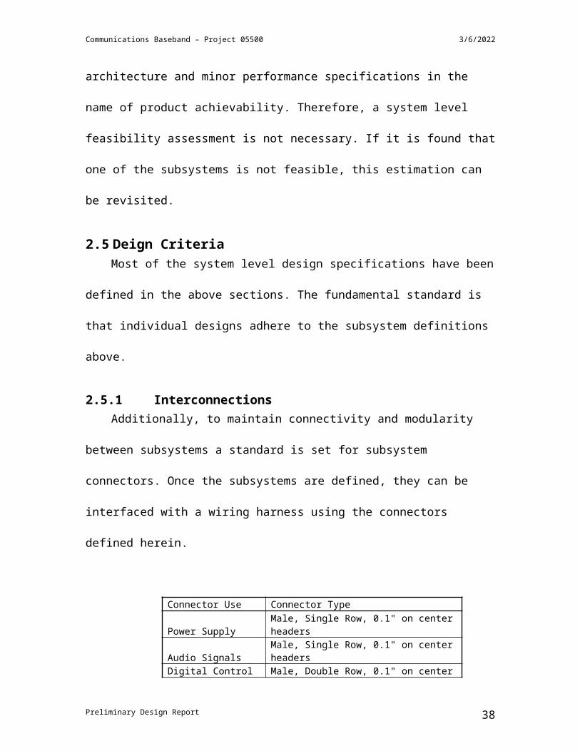
2.5.1 InterconnectionsAdditionally, to maintain connectivity and modularity between subsystems a
standard is set for subsystem connectors. Once the subsystems are defined, they can be
interfaced with a wiring harness using the connectors defined herein.
Connector Use Connector TypePower Supply Male, Single Row, 0.1" on center headersAudio Signals Male, Single Row, 0.1" on center headersDigital Control Lines Male, Double Row, 0.1" on center headersRF Signals Female, 50ohm, SMA
Table 3 – Subsystem Connector Types
Preliminary Design Report 25
Communications Baseband – Project 05500 5/8/2023
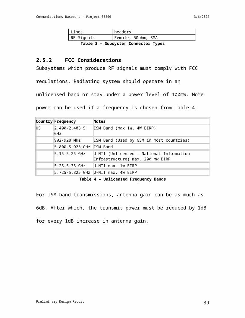
2.5.2 FCC ConsiderationsSubsystems which produce RF signals must comply with FCC regulations. Radiating
system should operate in an unlicensed band or stay under a power level of 100mW.
More power can be used if a frequency is chosen from Table 4.
CountryFrequency NotesUS 2.400-2.483.5 GHz ISM Band (max 1W, 4W EIRP) 902-928 MHz ISM Band (Used by GSM in most countries) 5.800-5.925 GHz ISM Band 5.15-5.25 GHz U-NII (Unlicensed - National Information Infrastructure)
max. 200 mw EIRP 5.25-5.35 GHz U-NII max. 1w EIRP 5.725-5.825 GHz U-NII max. 4w EIRP
Table 4 – Unlicensed Frequency Bands
For ISM band transmissions, antenna gain can be as much as 6dB. After which, the
transmit power must be reduced by 1dB for every 1dB increase in antenna gain.
Preliminary Design Report 26
Communications Baseband – Project 05500 5/8/2023
3 Audio SubassemblyThis section will introduce the input subsystem through all of its steps of design.
The conceptualization, mathematical basis, feasibility, and preliminary design will be
given.
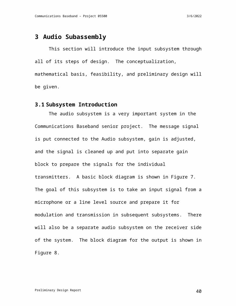
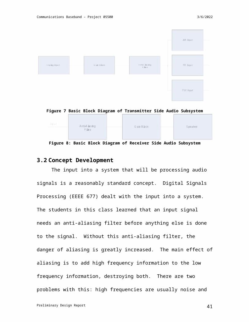
3.1 Subsystem IntroductionThe audio subsystem is a very important system in the Communications Baseband
senior project. The message signal is put connected to the Audio subsystem, gain is
adjusted, and the signal is cleaned up and put into separate gain block to prepare the
signals for the individual transmitters. A basic block diagram is shown in Figure 7. The
goal of this subsystem is to take an input signal from a microphone or a line level source
and prepare it for modulation and transmission in subsequent subsystems. There will also
be a separate audio subsystem on the receiver side of the system. The block diagram for
the output is shown in Figure 8.
Figure 7 Basic Block Diagram of Transmitter Side Audio Subsystem
Preliminary Design Report 27
Communications Baseband – Project 05500 5/8/2023
Figure 8: Basic Block Diagram of Receiver Side Audio Subsystem
3.2 Concept DevelopmentThe input into a system that will be processing audio signals is a reasonably
standard concept. Digital Signals Processing (EEEE 677) dealt with the input into a
system. The students in this class learned that an input signal needs an anti-aliasing filter
before anything else is done to the signal. Without this anti-aliasing filter, the danger of
aliasing is greatly increased. The main effect of aliasing is to add high frequency
information to the low frequency information, destroying both. There are two problems
with this: high frequencies are usually noise and once aliasing takes place, there is no
practical or theoretical method to recover the original signal.
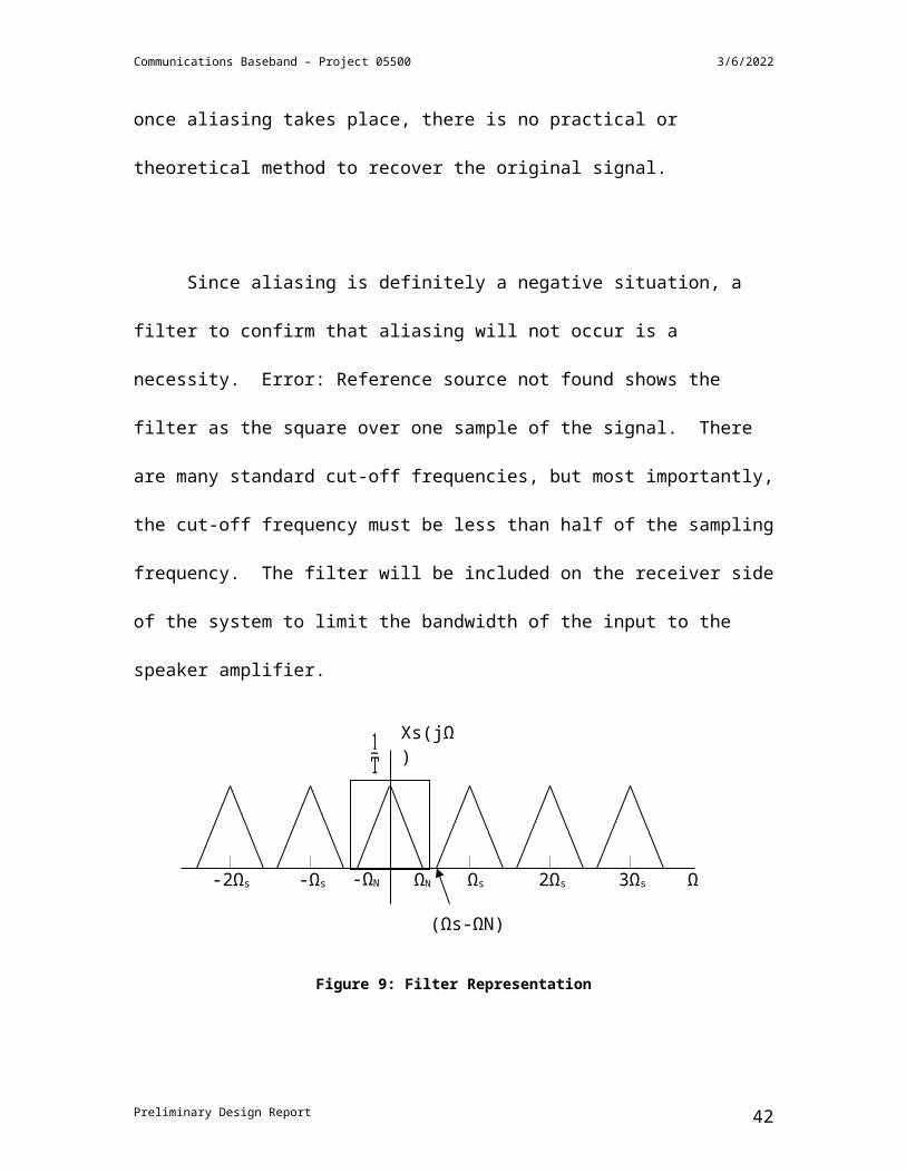
Since aliasing is definitely a negative situation, a filter to confirm that aliasing
will not occur is a necessity. Error: Reference source not found shows the filter as the
square over one sample of the signal. There are many standard cut-off frequencies, but
most importantly, the cut-off frequency must be less than half of the sampling frequency.
The filter will be included on the receiver side of the system to limit the bandwidth of the
input to the speaker amplifier.
Preliminary Design Report 28
Communications Baseband – Project 05500 5/8/2023
Figure 9: Filter Representation
The Digital Signals Processing class or textbook did not mention everything
necessary for a system to work; the class and textbook assumed the input message would
be equal to the input specifications every time. Unfortunately, in the physical world,
input voltages are changing. To properly deal with this, a gain block needs to be in the
system as shown in Figure 7. This gain block will be manually adjustable to
accommodate the listening needs of the end user.
3.3 Feasibility AssessmentThe feasibility of the audio subsystem is not in doubt. There are textbooks to
assist in the building of the filters and through experience gain blocks are easy to
construct.
3.4 Design ObjectivesThe design objectives are given in this section to assist in the design of each
component of the Audio Subsystem.
3.4.1 MicrophoneThe input device was the first piece of the audio subsystem looked at for the
objectives. The main objective here was the cost, power, and utility of the microphone.
Preliminary Design Report
Ω
Xs(jΩ)
ΩN -ΩN Ωs 2Ωs 3Ωs-Ωs-2Ωs
(Ωs-ΩN)
29
Communications Baseband – Project 05500 5/8/2023
If the microphone is quite easy to break, it would be a poor choice for a laboratory, since
items are accidentally dropped. The cost is the other major factor, since the project is
attempting to stay as low cost as possible. The microphone should have output voltages
of 0V to 5V, to allow the design of the next stage to continue. The input for the
microphone should be ¼ inch, rather than the higher end XLR. This is a standard plug
and thus will support other types of analog devices.
3.4.2 Gain BlockThe second stage of the Audio subsystem is the gain block. The input device will
have fluctuating input voltage amplitude, making the specifications for the next stage
harder to set. This block will allow the user to modify the input signal by a certain
amount of gain. The range in voltage should be 0V to 5V from the previous stage, but
the average speaking level of most people is between 1-3 V. The gain of this block
should be ½ up to five times the input level. This should be manually adjustable for the
user.
3.4.3 Low Pass FilterThe goal of this input subsystem is to take in voice information from a
microphone or to take in line level information from a CD player or other systems of that
ilk. Human ears can detect sounds from 30 Hz to 20 kHz, therefore any input frequencies
higher than that do not matter. The Human voice is approximately 200 Hz through 3.5
kHz. Since to most basic goal of the project is to use Human voice input through the
microphone, a low pass filter with a cut-off of 5 kHz would be sufficient. However, an
analog input device like a CD player uses the entire spectrum of Human hearing. To
accommodate this, a filter with a cut-off of 20 kHz would be best. The standard sampling
Preliminary Design Report 30
Communications Baseband – Project 05500 5/8/2023
rate for a CD is 44.1 kHz; if the same quality of sound from our digital system is desired
as from a CD, the maximum sampling frequency is 22.05 kHz. The filter is
overdesigned, using the stop-band as 22 kHz. For the design, the pass-band can have a
ripple of up to 0.5 dB. This translates into 94.4%-105.6% of the input signal level. The
stop-band was chosen to have 20dB of attenuation. This translates into 10% of the input
signal or less.
A low-order filter is desired. If the filter has too many orders (greater than 10) the
system is harder to implement using discrete parts. A filter that is only a fourth or fifth
order would be optimum for this design. Those two orders are chosen for their ability to
filter well, offset by the difficulty to design and implement. An easy method to reduce
the order of the filter would be to use active components, but doing so would increase the
design time and understanding necessary to successfully achieve the desired results. The
design will be limited to Op-Amps and passive components.
3.4.4 High Power Op-AmpA high-power Op-Amp is needed to drive a speaker, or other parts of the project
that require a large amplification of a signal. The minimum requirement is a single
channel output, but a double channel output leaves room for expansion in the future. The
low-cost alternative is a desired result.
3.4.5 SpeakerThe speaker must be able to handle the input conditions from the High-Power Op-
Amp. Price and size are also considerations, with price being more heavily weighted.
3.5 Design SynthesisThis section describes the design of each component in the Audio subsystem.
Preliminary Design Report 31
Communications Baseband – Project 05500 5/8/2023
3.5.1 MicrophoneThree brands of microphones were analyzed for their usefulness for this project:
Peavey, Radio Shack and Nady. Peavey is a brand that is well known for its quality audio
equipment, so their website was visited first. Unfortunately, with a brand well known for
quality, the low price equipment is usually lacking. The Peavey PVi 100 started at
$29.99 which is too expensive for a simple input microphone, especially considering the
shipping prices of about $4. Radio Shack is the second website visited. Their
Unidirectional Dynamic Microphone costs $19.99 and there is no shipping. This seems
to be a good choice, because Radio Shack has a known quality level and it is sufficient
for this project. Nady is a brand that is known for its quality microphones are low prices.
A search of their website, yielded the SP-3 StarPower microphone. However, their
website is lacking and a price quote was not available. A quick search of American
Music Supply yielded a price of $17.95 plus shipping and handling of about $5. The
Radio Shack microphone was found to be the best microphone for the purpose.
3.5.2 Op-AmpThe design will use LM741 Op-Amps that are capable of receiving a ±15 V
signal. The price is $0.68 and there is one Op-Amp per 8 pin DIP. Using a
potentiometer and a resistor, the gain will be able to be adjusted from ½ to 5. The
potentiometer will be adjustable between 5 kΩ and 50 kΩ while the resistor will be a 10
kΩ resistor. The system will be set-up as shown in Figure 10.
Preliminary Design Report 32

Communications Baseband – Project 05500 5/8/2023
+3
-2
V +8
V -4
O U T1
U 1 A
L M 7 4 1
0
R 1
1 0 k
In p u t
Output
R 3
5 k -5 0 k
V 11 2 V d c
V 21 2 V d c
0
0
Figure 10: Op-Amp in Gain Formation
3.5.3 Low Pass FilterThe textbook referenced in this section is: Design of Analog Filters by Rolf
Schaumann and Mac E. Van Valkenburg.
3.5.3.1 Butterworth FilterIn designing filters, the first step is to try a simple filter. The first filter attempted
is the Butterworth Filter. The design equations follow:
Equation 3.5.3-1
Equation 3.5.3-2
Using the design specifications and the design equations 1 and 2, n (the order of
the filter) is found to be 36. A 36th order filter does not meet the design specification of
being a low-order filter.
3.5.3.2 Elliptical FilterThe next filter attempted is an Elliptical Filter. The design equations follow:
Preliminary Design Report 33
Communications Baseband – Project 05500 5/8/2023
Equation 3.5.3-3
Equations 3.5.3-4a and 4b
Using Design Figure 8.16:
n=4
A fourth order filter is within the design specifications for the Low-Pass Filter. Using
Design Table 8.5, the transfer function of the filter is:
Equation 3.5.3-5
The schematic or this original transfer function is shown in Figure 11. The frequency
output is shown in Figure 12.
R 1 5
9 . 2 1 k
R 1 6
7 . 9 6 k
+3
-2
V+
7V
-4
O U T6
O S 11
O S 25
U 5
LM 7 4 1
+3
-2
V+
7V
-4
O U T6
O S 11
O S 25
U 6
L M 74 1
C 7
.6 1 n
C 81n
C 9.3 9n
R 1 7
1 2 9 . 1k
R 1 8
7 . 7 6 k
R 1 9
7 . 7 6 k
R 2 0
7. 7 6 k
R 2 13 1 0 . 4k
R 2 21 2 2 . 8k
V 1 012 V d c
V 1 112 V d c
0
V 1212 V d c
V 1312 V d c
0
0
0
+3
-2
V+
7V
-4
O U T6
O S 11
O S 25
U 7
L M 74 1
+3
-2
V+
7V
-4
O U T6
O S 11
O S 25
U 8
L M 7 4 1
C 1 0
.7 8 n
C 1 11n
C 1 2.2 2 n
R 2 3
1 5 .9 k
R 2 4
8 . 9 8 k
R 2 5
8. 9 8 k
R 2 6
8 . 9 8 k
R 2 73 5 9 . 2k
R 2 815 .1 2 k
V 141 2 V dc
V 151 2 V dc
V 1612 V d c
0
V 1712 V d c
0
0
0
0
0
V 1 85V a c0V d c
Figure 11: 1st Iteration LPF Schematic
Preliminary Design Report 34
Communications Baseband – Project 05500 5/8/2023
Frequency
1.0KHz 3.0KHz 10KHz 30KHz 100KHzV(V18:+) V(R19:2)
0V
1.0V
2.0V
3.0V
4.0V
(20.380K,1.6566)
(22.109K,276.094m)
Figure 12: 1st Iteration LPF Frequency Response
The second iteration of the design process used new, realistic values for the
resistors and capacitors, attempting to get a real working filter. The resistor values were
tweaked, rounded, and re-simulated to find working values. The output schematic is
shown in Figure 13. The frequency response is shown in Figure 14.
R 5
1 0 k
R 8
1 0 k
+3
-2
V+
7V
-4
O U T6
O S 11
O S 25
U 3
LM 7 4 1
+3
-2
V+
7V
-4
O U T6
O S 11
O S 25
U 4
L M 74 1
C 4
.6 2 n
C 51n
C 6.3 9n
R 9
1 2 0k
R 1 0
8 . 2 k
R 1 1
8 . 2 k
R 1 2
8 . 2 k
R 1 33 3 0k
R 1 41 2 0k
V 612 V d c
V 712 V d c
V 812 V d c
0
V 912 V d c
0
0
0
+3
-2
V+
7V
-4
O U T6
O S 11
O S 25
U 1
L M 74 1
+3
-2
V+
7V
-4
O U T6
O S 11
O S 25
U 2
L M 7 4 1
C 1
.7 5 n
C 21n
C 3.2 2 n
R 1
1 5 k
R 2
8 . 2 k
R 3
8. 2 k
R 4
8 . 2 k
R 63 3 0k
R 715 k
V 11 2 V dc
V 21 2 V dc
V 312 V d c
V 412 V d c
0
0
0
0
0V 55V a c0V d c
0
VV
V
Figure 13: 2nd Iteration LPF Schematic
Preliminary Design Report 35
Communications Baseband – Project 05500 5/8/2023
Frequency
1.0KHz 3.0KHz 10KHz 30KHz 100KHzV(V18:+) V(R19:2)
0V
1.0V
2.0V
3.0V
4.0V
(20.434K,1.6498)
(22.103K,289.562m)
Figure 14: 2nd Iteration LPF Frequency Response
3.5.4 High Power Op-AmpTo find a suitable option for a High-Power Op-Amp, company websites were
searched. The first page searched was the Motorola web page (www.motorola.com). No
choices were available on the website. The second website searched was for National
Semiconductor (www.national.com), which yielded the LM1877 Dual Audio Power
Amplifier. This option has the ability to output 2W into two separate 8Ω loads. This
meets the design requirements, and provides more functionality for future upgrades. The
cost of this part on Digi-Key (www.digikey.com) is $1.55, which qualifies as low cost.
Due to National Semiconductor’s educational policy, free samples were available for
students.
3.5.5 SpeakerTo find the desired speaker, Digi-Key (www.digikey.com) was searched using the
parameters of 3W at 8Ω. 3W was chosen to make sure the speaker is not overdriven.
Two speakers matched these specifications, in two different sizes. The larger speaker is
Preliminary Design Report 36

Communications Baseband – Project 05500 5/8/2023
90mm x 50mm and the smaller speaker is 12mm x 60mm. The smaller speaker is $6.05,
while the larger speaker is $4.54. The larger speaker is chosen because of its lower cost,
while still satisfying the other design specifications.
3.6 Preliminary System DefinitionThis section is composed of the preliminary drawing packages, assembly and
component packages, the bill of materials and supplier information, and the overall
specifications for the Audio Subsystem.
3.6.1 Preliminary Drawing PackagesThe preliminary drawing packages are throughout Chapter 3. Figure 7 is a basic
block diagram of what the input audio subsystem does in total. Figure 8 is a basic block
diagram of the output audio system. These figures completely represent what the audio
subsystem does in this project. The blocks show the simplest functions to be performed.
3.6.2 Assembly and Component PackagesThis section will contain the element by element schematics with the specific part
numbers on each part.
+3
-2
V+
8V
-4
O U T1
U 1 A
L M 7 4 1
0
R 1
1 0 k
Output
R 3
5 k -5 0 k
V 11 2 V d c
V 21 2 V d c
0
0Catalog # 33-3021Radio ShackUnidirectional Dynamic Microphone
Catalog # 274-312Radio Shack1/4 panel jack
Anti-AliasingFilter
Figure 15: Audio Subsystem Circuit Diagram
Preliminary Design Report 37
Communications Baseband – Project 05500 5/8/2023
The majority of the Audio subsystem is displayed in Figure 15. The filter block is
Figure 13 and is already displayed in the previous section, with all of the necessary
component part numbers and values to be used in the construction of the Audio
Subsystem in the Spring Quarter 2005.
3.6.3 Bill of Materials and SuppliersTable 5shows the Bill of Materials and Suppliers for the current design.
Table 5: The Bill of Materials and SuppliersItem Supplier Quantity Cost Part Number
Unidirectional Dynamic Microphone Radio Shack 1 19.991/4 inch Panel-Mount Jack Radio Shack 1 3.99LM741 Digikey 5 0.68 LM741CNNS-NDPotentiometer Digikey 1 2.32 P4F4502-ND
LM1877 High Power Op-AmpNational Semiconductor 2 **free**
Speaker Digikey 1 4.54 P10186-ND10k Ceramic Resistor Digikey 3 0.76 OX103K-ND8.2k Ceramic Resistor Digikey 6 0.76 OX822K-ND330k Ceramic Resistor Digikey 2 1.17 OY334K-ND120k Ceramic Resistor Digikey 2 1.17 OY124K-ND15k Ceramic Resistor Digikey 2 0.76 OX153K-ND750 pF Ceramic Capacitor Digikey 1 1.32 511-1158-1-ND220 pF Ceramic Capacitor Digikey 1 1.32 511-1146-1-ND1 nF Ceramic Capacitor Digikey 2 1.32 511-1164-2-ND620 pF Ceramic Capacitor Digikey 1 0.94 490-1446-1-ND390 pF Ceramic Capacitor Digikey 1 1.32 511-1152-2-ND
3.6.4 Overall SpecificationsThe overall specifications are all listed in Table 6.
Table 6: Overall Specifications
Input Units
Input Voltage 0-5 V
Input Jack ¼ cable -
Output Voltage Adjustable V
Output Jack SMA -
Preliminary Design Report 38
Communications Baseband – Project 05500 5/8/2023
4 AM SubassemblyThe AM subassembly is one of the three different transmission methods used in
this senior design project. The AM stands for Amplitude Modulation and is a specific
form of modulation. This chapter will display the concept development, feasibility
assessment, design objectives and design procedure used in the Winter Quarter of 2004-
2005.
4.1 Subsystem IntroductionIn the AM subassembly there are 2 sections: transmit and receive. In the AM
transmitter, there are 5 major blocks: the oscillator, two buffer amplifiers, the modulated
amplifier, the RF power amplifier, and the antenna. The oscillator supplies the carrier
wave that will be modulated by the input. The buffer amplifier and the audio amplifier
are to isolate the previous blocks from the modulator. The modulator is the device that
will actually mix the message signal with the carrier signal, creating the AM signal. The
RF power amplifier will be used to boost the modulated signal to a level that will
broadcast the signal to the receiver. The block diagram is shown in Figure 16.
The AM receiver is much simpler than the transmitter setup. An antenna receives
the signal and passes it to an envelop detector that will detect the incoming signal and
automatically demodulate the signal. A gain block will be placed on the end of this
circuit to boost the power of the signal to a 0-5V output. The block diagram is shown in
Figure 17.
Preliminary Design Report 39
Communications Baseband – Project 05500 5/8/2023
Figure 16: Basic Block Diagram of AM Transmit Subsystem
Figure 17: Basic Block Diagram of AM Receive Subsystem
4.2 Concept DevelopmentThere were three major ideas when choosing the method for the AM subsystem
was broached: a discrete parts design, separate integrated circuits (ICs), or a transceiver
IC. The following concepts are discussed in this section, as well as the receiver circuit.
Once one of these methods is chosen, the rest of the blocks are designed to fit in with the
chosen method.
4.2.1 Discrete Parts DesignTo do a design of an AM modulator using discrete parts, a large knowledge of
analog circuit design is required. There are a number of textbooks available in the
library, as well as designs on the internet that would be able to help. Some of the
positives to using this style of AM transmission include the increased knowledge of how
Preliminary Design Report 40
Communications Baseband – Project 05500 5/8/2023
to design analog circuits for non-ideal situations and the cost. The cost of a number of
discrete parts usually will be less than that of a few ICs or one transceiver IC. A
drawback is that troubleshooting the circuitry, if something does not work properly, will
be extraordinarily difficult. Another advantage of using a discrete part design is the
ability to design the circuit for whatever frequency is desired.
4.2.2 Separate Integrated CircuitsThere are advantages and disadvantages to using many different ICs in the AM
transmitter circuitry. One of the advantages is the ease of finding separate ICs to perform
the specific task. An IC that just does mixing and another IC that just does RF power
amplifying is much easier to find than one IC that will do both. Especially since AM
transistor radios are more than 30 years old, the ability to find parts to specifically create
an AM radio is getting more difficult. The demand has gone down for AM radio ICs
because FM dominates the radio market. An advantage of the separate IC design method
is the easy visualization of the block diagram on the circuit board after the layout is
complete. The ability to closely control the output of the system is an advantage of the
separate IC method of design. A disadvantage is the external circuitry required to make
many IC work according to their specifications. Most datasheets include sample
circuitry, but the circuits are often incomplete, un-updated, or contains incorrect
component values. The ability to choose one IC over another when there is a myriad of
choices is difficult. The knowledge of superior characteristics for a specific part is quite
esoteric. The differences between three ICs from three different companies are slight and
choosing the one to fit into the project is difficult.
Preliminary Design Report 41
Communications Baseband – Project 05500 5/8/2023
4.2.3 Transceiver Integrated CircuitAn AM Transceiver IC combines all parts of the AM transmitter set into one IC,
with enough power to output a signal across a laboratory. An advantage of this IC is the
lack of connections to other ICs and the troubleshooting that goes with this. With all
functions performed in this chip, the size of the final board could be much smaller.
Another advantage of this option is the lack of design choices to overload the design
process. With specified input and output requirements, the input and output systems have
detailed design goals. The largest advantage of the AM Transceiver IC is that the
receiver chip would already be selected and its functionality with the transmitter is
assured. The only AM Transceiver on the market currently is the MC13190, which
operates at 2.4 GHz. With current market trends, the design experience of dealing with
S-Band is highly desirable. The largest disadvantage of the AM Transceiver is the need
for a surface mount PCB board. The cost of producing the board is high as well as time
consuming for the designer. The required skill for soldering a surface mount IC is quite
high and needs very small solder joints.
4.2.4 Receiver CircuitThere are three major methods to deal with the reception and demodulation of the
AM signal. Discrete Components, a Receiver IC and the receive part of the Transceiver
IC. The receiver part of the Transceiver is discussed in section 4.2.3. The discrete
components can be made easily and designed easily, but the function of such an easy
circuit is in question. The only demodulator circuit available in the textbooks consulted
is the basic envelope detector, shown in Figure 18. A disadvantage of the Receiver IC is
the lack of availability due to the popularity of FM. The advantages of the IC are the
Preliminary Design Report 42
Communications Baseband – Project 05500 5/8/2023
ease of use and the guarantee that they work when properly arranged. A disadvantage is
the possible difficulty in properly arranging the supporting circuitry.
V 1
1 2D 1 C 1 C 2
R 1 R 2
Figure 18: Envelope Detector
4.3 Feasibility AssessmentThe choices laid out in section 4.2 each have their advantages and disadvantages,
but using a weighted comparison method, the best choice is easily found.
4.3.1 AM Transmitter SubsystemDue to the weighting of the completion by May design objective, the choice for
the AM Transmitter Subsystem is the separate ICs. The ability to find parts for this
method is much more secure than the other two options. The chance of free samples is
quite high for many of the parts, in a ploy by the semiconductor companies to increase
their business for production level designs. The disadvantages will be overcome using
design choices. The disadvantage of too much external circuitry will be overcome by
choosing ICs that require little or none external circuitry. Finding these parts can be
difficult, but the effort at the outset pays out when the circuit is being constructed.
Choosing between parts that are very similar will be done with the help of an experienced
engineer.
Preliminary Design Report 43
Communications Baseband – Project 05500 5/8/2023
4.3.2 AM Receiver SubsystemSince the AM Transmitter is chosen as using separate ICs, choosing the Receiver
circuit to match is a logical selection. There is the possibility to test, for added
understanding, the envelope detector if the project is nearing completion well before the
end of the quarter. However, the Receiver IC is not posted in a theoretical textbook, but
is known to work correctly. The IC will be chosen to minimize the external circuitry
necessary. A small company in Rhode Island has been found to sell AM Receiver ICs,
overwhelming the disadvantage of finding AM Receivers.
4.4 Design ObjectivesThis section will give the design objectives for each of the blocks necessary for
the successful completion of the AM Transmitter and Receiver. The blocks for the
transmitter include: a clock oscillator, buffer amplifiers, modulator, power amplifier, and
antenna. The receiver blocks include an antenna and an AM receiver.
4.4.1 Clock OscillatorThe clock oscillator is the component in the AM circuitry that will supply the
carrier signal to the rest of the module. The output needs to be at least an approximation
of a sine wave for proper AM modulation. The frequency of this component is the
determining frequency for the rest of the AM system. The AM modulation can be done
on any frequency; standard AM broadcast frequencies are 530 kHz to 1700 kHz. For this
reason, the frequency is chosen at 1 MHz (1000 kHz). At 1 MHz, the frequency band in
Rochester, NY (the operational location) is relatively clear, thus leading to less
interference. Low-cost option is a desire.
Preliminary Design Report 44
Communications Baseband – Project 05500 5/8/2023
4.4.2 Buffer AmplifiersThe output for the clock oscillator will be disturbed by the input impedance of the
modulation block, so the oscillator will need to be buffered by a unity gain amplifier.
The use of a buffer amplifier on the audio input is twofold; to be sure the input resistance
does not interfere with the operation of the audio subsystem and to assure proper
modulation levels. The gain of this block will probably be less than 1, just to guarantee
the circuit does not overmodulate.
4.4.3 ModulatorThe modulator for the AM system needs to be able to modulate the carrier and the
message signals into a correct AM signal. The input voltage levels will be a maximum 0-
5V for both signals, with the message signal being a bit lower than the carrier signal.
This IC should be able to output a signal that can be increased by a power amplifier to be
broadcast across the laboratory. The minimum amount of external circuitry is a priority.
Low-cost is a desire for the design.
4.4.4 Power AmplifierThe design of the power amplifier relies greatly on the choice of the modulator.
The output voltage of the amplifier should be no more than 4 dBm or 2.4 mW. This
amount of power is more than enough to go up to 10 meters and beyond. The IC should
be able to accept anything the modulator can output. The bandwidth of the IC should be
high to accommodate signals with a lot of information. The output of the power
amplifier will go to an SMA connector.
Preliminary Design Report 45
Communications Baseband – Project 05500 5/8/2023
4.4.5 AntennaThe antenna for the AM Transmitter and Receiver will be the same antenna for
each side. AM frequencies do not require large antennas in general. The connector on
the antenna must be SMA for easy analysis by students who will be the end users of this
product.
4.4.6 AM ReceiverAn AM receiver must be able to operate at the frequency chosen for the circuit, as
well as have enough sensitivity to detect the input signal. The part should be available in
United States for a reasonable price.
4.5 Design SynthesisThis section is an in depth look at the design process for the AM Transmitter and
Receiver. The blocks covered are the Clock Oscillator, the Buffer Amplifiers, the
Modulator, the Power Amplifier, the Antennas, and the AM receiver.
4.5.1 Clock OscillatorThere are two main options for an oscillator: Clock oscillator or a Crystal
oscillator. The first specification is a 1 MHz signal. Looking at Digi-Key,
(www.digikey.com) there is a selection of both crystal and clock oscillators at the design
frequency. The next specification is the sine wave. At a first look, the crystal oscillator
is the best option, because it has a steady output of a sine wave. The clock oscillator has
a pulsed output. However, the pulsed output can be changed into an approximate sine
wave using a simple L-C filter. The third specification is price. The crystal oscillator at
this frequency cost $17.88, while the clock oscillator cost $1.88. In this category, the
clock oscillator is a clear winner. As a bonus, the clock oscillator is a much easier
Preliminary Design Report 46
Communications Baseband – Project 05500 5/8/2023
component to use, with only 4 pins going to the PC board. The crystal oscillator needs
supporting circuitry to fully operate as designed. Figure 19 shows the clock oscillator
and the RLC filter over 10 periods.
Time
40us 41us 42us 43us 44us 45us 46us 47us 48us 49us 50usV(R1:1) V(C1:2)
0V
0.5V
1.0V
1.5V
2.0V
2.5V
3.0V
Figure 19: Clock Oscillator and RLC Filter
4.5.2 Buffer AmplifiersThe buffer amplifiers are very similar to the Op-Amp in section 3.5.2. The main
difference is the potentiometer. The amplifiers in the AM Transmitter is not going to
need to be manually controlled. The unity gain amplifier will have equal values for each
resistor at 10 kΩ. The modulation factor (depth of modulation) needs to be picked to
design for the audio buffer amplifier. To have the maximum power transmitted to the
receiver in a double sideband transmission, the m should be equal to 1. However, if the
value of m is higher than 1, the signal is overmodulated and data is lost. To be
guaranteed that m is not greater than 1 at any time, the modulation factor should be equal
to 0.8. The depth of modulation is equal to the voltage of the message divided by the
Preliminary Design Report 47

Communications Baseband – Project 05500 5/8/2023
voltage of the carrier signal. The voltage of the carrier supply is 2.4 V from the clock
oscillator. Therefore, the voltage from the message should be equal to 0.8 times 2.4V.
This works out to 1.92V. The resistor values should work out to be approximately a ratio
of 2 to 5. Resistor values that fit that specification are 8.2 kΩ and 22 kΩ.
4.5.3 ModulatorsFinding an AM modulator is a difficult process of searching different
semiconductor company’s websites looking for a part that may or may not be made
anymore. The MC13175 was found on the same website as the AM receiver. The
sample diagram in the datasheet is for a 320 MHz AM Transmitter, which is a much
higher transmit frequency than desired. The circuit also uses a loop antenna and a 50Ω
balun. The use of crystal oscillators also increases the difficulty of implementation, due
to the exacting tolerances for resistors and capacitors. The MC13175 was rejected for
these reasons. While looking for AM Receivers, a TDA part was found, so following that
lead, a TDA AM Modulator was searched for on the Philips Semiconductor website.
Unfortunately, a TDA AM modulator does not seem to exist. The next semiconductor
website searched was ON Semiconductor. This search yielded the MC1496 Balanced
Modulator/Demodulator. Looking through the datasheet, this IC appears do be able to
function successfully. A figure in the datasheet is an example AM Modulator circuit,
possibly making the functional design easier. However, the previously noticed
disadvantage of incomplete or wrong sample diagrams seems to be true in this circuit. To
assist in the choosing of a modulation IC, a senior analog design engineer was contacted
and queried. The recommendation was to use an analog mixer from Analog Devices,
specifically one of the model numbers AD633 or AD835. After looking at the datasheets
Preliminary Design Report 48
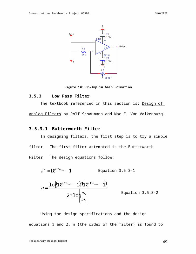
Communications Baseband – Project 05500 5/8/2023
for each, the AD835 was selected. The superior bandwidth and supply voltages both
counted in its favor. The cost was not a factor because Analog Devices is another
company that will send a few sample ICs to assist in the design and testing of circuits.
4.5.4 RF Power AmplifierThe design for the RF Power Amplifier is chosen to be an Analog Devices part, to
match the modulation unit. The original part chosen is the AD621. The problem with
this IC is the bandwidth is too limited. An 800 kHz bandwidth may be enough, but there
are better power amplifiers. After consulting with the senior analog design engineer, the
AD8056 was recommended through good personal experience. The bandwidth for the
AD8056 is a much larger 300 MHz. The implementation is just like a High Power Op-
Amp. With an output of 60mA and 40V, the design objective of 2.4 mW is easily
reached.
4.5.5 AntennasAM antennas are not difficult to design at a frequency of 1 MHz. Approximately
30 inches of wire is enough to radiate the signal and retrieve it at the receive side. The
antenna needs to be attached to a SMA connector, for ease of analysis by future students.
4.5.6 AM RecieverTo find a suitable AM receiver there was a large amount of searching company
web pages. Each of the large semiconductor companies (Motorola www.motorola.com,
Freescale Semiconductor www.freescale.com, National Semiconductor
www.national.com, ON Semiconductor www.onsemi.com, Fairchild Semiconductor
www.fairchildsemi.com, and Maxim www.maxim-ic.com) were queried for their own
AM receiver. However, each of these companies since the late 80’s, has not fabricated
Preliminary Design Report 49
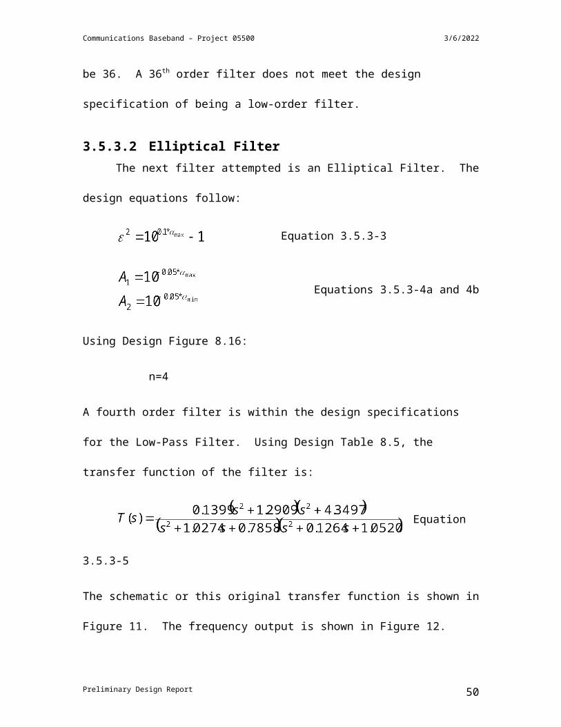
Communications Baseband – Project 05500 5/8/2023
any AM receivers because of the competition from the Far East. Using Google, an AM
receiver was mentioned; this is the TDA 1072 made by Philips. A search was performed
to find a data sheet and a seller of the TDA 1072. The data sheet was found, with a
copyright of 1987, but there was only one American seller. This obsolete IC dealer
would not bid on selling his TDA 1072 stock. A search was then made of the Philips
semiconductor website, which revealed another AM receiver which is in current
production. The TDA1572T is in full production, but after searching, the possibility of
purchase does not exist. Only two American dealers had the TDA1572t available for
purchase, but both prominently displayed messages stating their requirement for $100
minimum purchases. On a small electronics company’s site, another AM receiver was
found. The ZN416E is an AM receiver fabricated by a company called GEC Plessey
Semiconductors. The operating range for this component is 15 kHz to 3 MHz, within
which the 1 MHz design frequency falls. Most importantly, the part is available for
purchase within North America.
4.6 Preliminary System DefinitionsThis section is composed of the preliminary drawing packages, assembly and
component packages, the bill of materials and supplier information, and the overall
specifications for the AM Transmitter and Receiver Subsystems.
4.6.1 Preliminary Drawing PackagesThe basic block diagrams for the AM subsystem are shown in Figure 16 and
Figure 17. These two diagrams effectively show the overall subsystem clearly.
Preliminary Design Report 50
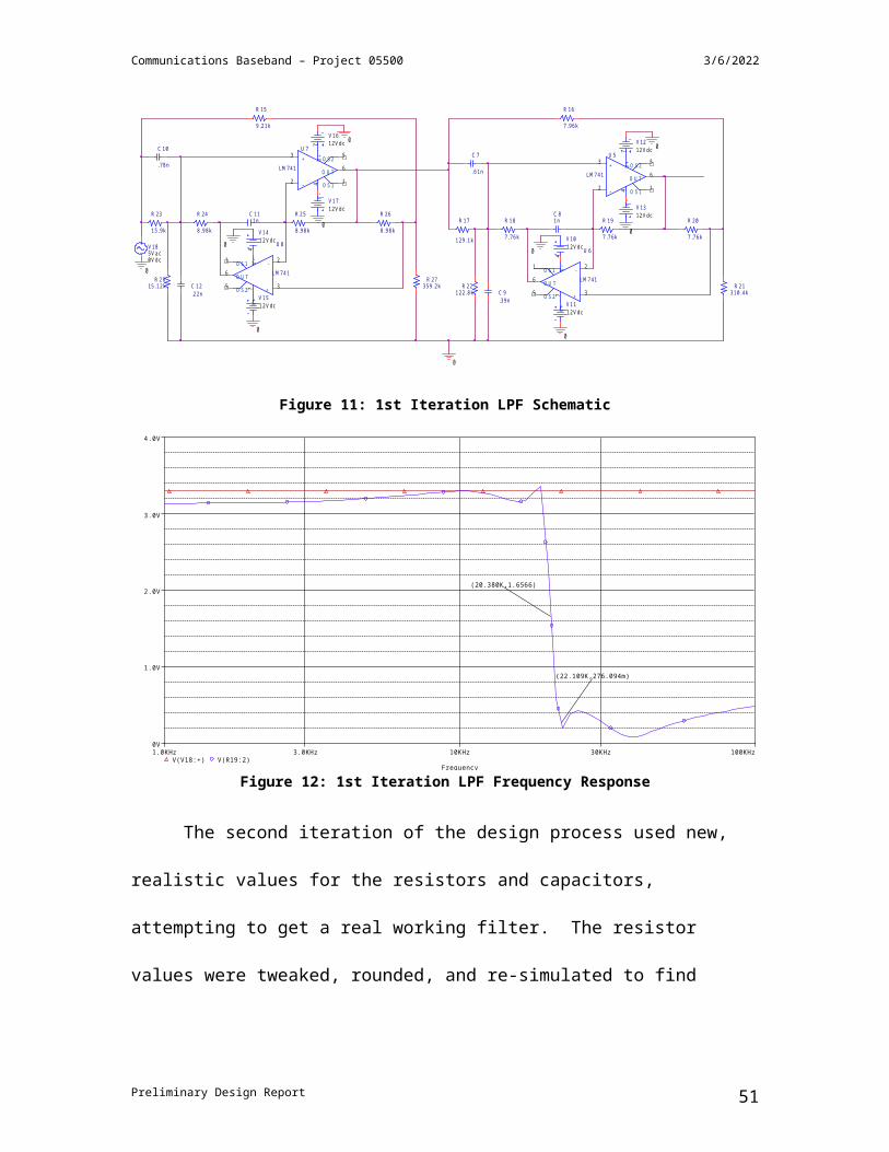
Communications Baseband – Project 05500 5/8/2023
4.6.2 Assembly and Component PackagesThis section will contain the element by element schematics with the specific part
numbers on each part.
R 1
6 2 0
C 12 7 0 p F
1 2L 1
1 0 0 u H
V 1TD = 0
TF = 1 0 nP W = 5 0 0 nP E R = 1 u
V 1 = 0 . 4
TR = 1 0 n
V 2 = 2 . 4
0
R 2
1 0 k
R 3
1 0 k
+3
-2
V+
8V
-4
O U T1
U 2 A
L M 7 4 1
V 21 2 V d c
V 31 2 V d c
0
0
Clock Oscillator Output
Figure 20: Clock Oscillator and Buffer Amplifier
R 2
1 5 k
R 3
1 2 k
+3
-2
V +8
V -4
O U T1
U 2 A
L M 7 4 1
V 212 V d c
V 312 V d c
0
0
Output
V a u d io
0
Figure 21: Audio Input Buffer
Preliminary Design Report 51
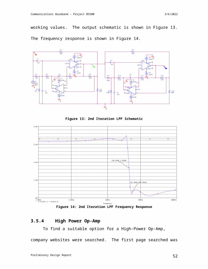
Communications Baseband – Project 05500 5/8/2023
+
-
O U T
U 3
O P A M P
+
-
O U T
U 4
O P A M P
1 2
U 5
IN V
VnVp
+
-
O U T
U 6
O P A M P
+
-
O U T
U 7
O P A M P
0
R 4
1 0 k
R 51 0 k
V 41 2 V d c
V 51 2 V d c
00
Message Circuitry
Carrier Circuitry
AD8056AD835
Figure 22: Mixer, RF Amplifier, and Antenna
0
C 10 . 1 u F
C 20 . 1 u F
C 30 . 4 7 u F
C 40 . 1 p F
C 50 . 1 u F
V 61 2 V d
1 8
7
6
54
3
2
ZN416EOutput
Figure 23: Antenna and AM Receiver
Preliminary Design Report 52
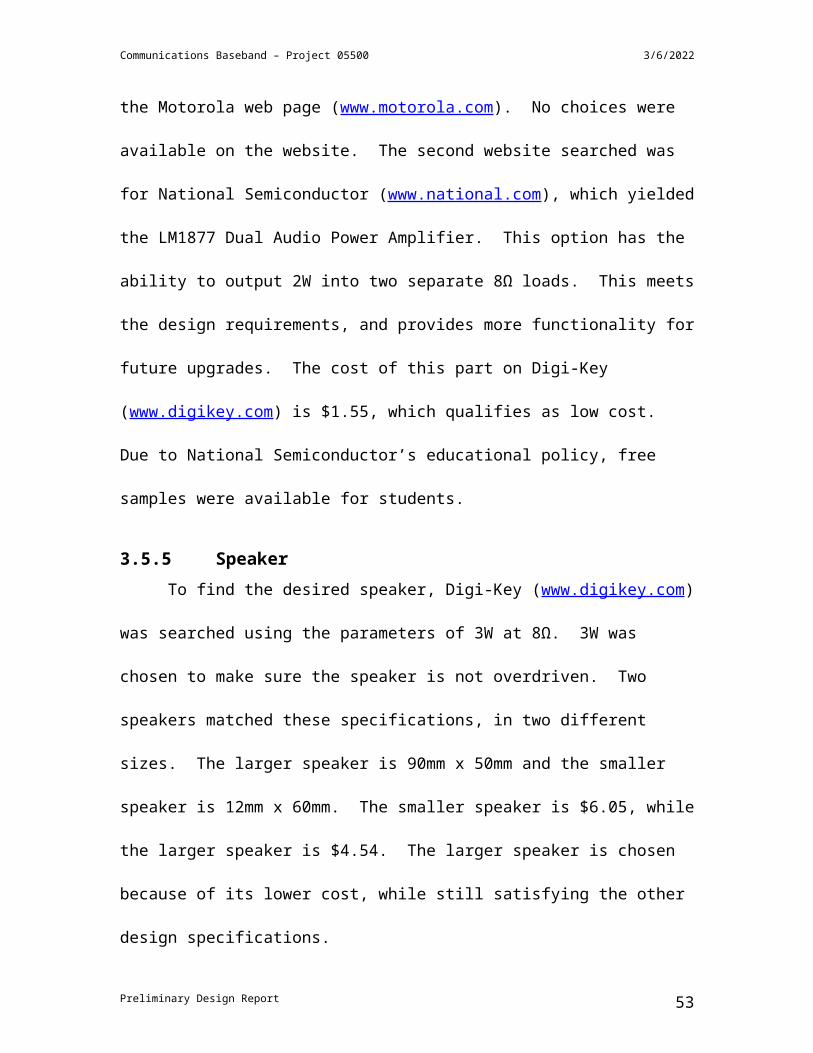
Communications Baseband – Project 05500 5/8/2023
4.6.3 Bill of Materials and SuppliersTable 7shows the Bill of Materials and Suppliers for the current design.
Table 7: Bill of Materials and SuppliersItem Supplier Quantity Cost Part Number
AD835 Analog Devices 1 $8.90 *free* AD835ANAD8055 Analog Devices 1 $1.60 *free* AD8056AN
ZN416EOcean State Electronics 1 $10.95 ZN416E
LM741 Digikey 2 0.68 LM741CNNS-ND10k Ceramic Resistor Digikey 4 0.76 OX103K-ND15k Ceramic Resistor Digikey 1 0.76 OX153K-ND680 Ceramic Resistor Digikey 1 0.76 OX681K-ND100uH Inductor Digikey 1 0.54 M7837-ND270 pF Ceramic Capicator Digikey 1 3.36 P10809-ND0.1uF Ceramic Capicator Digikey 4 0.34 399-2048-ND0.47uF Ceramic Capicator Digikey 1 0.83 399-2100-ND
4.6.4 Overall SpecificationsThe overall specifications are all listed in Table 8.
Table 8: Overall Specifications
Value Units
Input Voltage 0-5 V
Input Jack .1” header -
Max Output Voltage +4 dBm
Output Jack SMA -
Preliminary Design Report 53
Communications Baseband – Project 05500 5/8/2023
5 FM SubassembliesThis section includes the development of both the FM transmitter and receiver
sections. These systems are defined in sections 2.3.1.5 and 2.3.1.6.
5.1 Conceptual DesignFrequency modulation is a when the message signal is stored in the frequency of the
carrier signal. When no message is being conveyed, the carrier frequency stays at a
constant value (say 100MHz). To send a message on the carrier using frequency
modulation, the frequency of the carrier is changes proportionally with the amplitude of
the message signal. Figure 24 shows an example of a carrier modulated by a message
signal.
Figure 24 – Frequency Modulation of a Carrier
The equation for a frequency modulated signal shows the message signal added to
the frequency of the carrier. That is:
Preliminary Design Report 54
Communications Baseband – Project 05500 5/8/2023
The fundamental building blocks of an FM transmitter and receiver can be found in
Figure 25 and Figure 26.
Figure 25 – Basic FM Transmitter
Figure 26 – Basic Superheterodyne FM Receiver
5.2 Preliminary Feasibility AssessmentIt takes a great deal of time and knowledge to engineer a stable and reliable FM
transmitting and receiving system as outlined in section 5.1. In industry, an experienced
engineer can take months planning, designing, building, and refining similar systems.
This team only has one engineer assigned to these systems and his time is divided
between the FM and FSK tasks. Therefore it would not be feasible to design the above
systems from scratch.
Preliminary Design Report 55
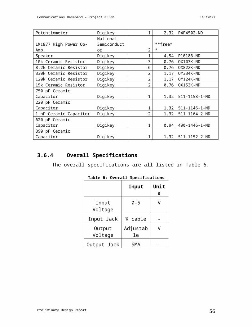
Communications Baseband – Project 05500 5/8/2023
5.3 Concept DevelopmentThe simplest solution would be a mixed signal IC. There is a range of IC available
which contain all the necessary building blocks for a stable and reliable RF system. They
include the necessary amplifiers, oscillators, modulators, demodulators (PLL’s), mixers,
and other pieces. Sometimes the only external parts necessary are RF loop and front end
filters.
A set of objectives were formulated for selecting a mixed signal IC. The objectives
were then weighted based on their importance for performance and feasibility. They are
outlines in Table 9.
Objective WeightPart availability 10Comprehensive design resources 8Application examples 7Performance 6Price 5Low parts count 5
Table 9 – Analog FM Part Selection Objectives
Next, a verity of popular mixed signal IC’s were research and they were rated (from
0 to 10) based on compatibility with the objectives in Table 9. The scores were then
multiplied by the weights of the objectives and tabulated. This analysis can be found in
Table 10.
Preliminary Design Report 56
Communications Baseband – Project 05500 5/8/2023
Table 10 – Analog FM Part Analysis
The BA1404 Transmitter is the current choice for FM broadcast. It is widely used,
has many application examples and is currently available for sale for only $6.95 from
Ocean State Electronics.
The TDA7000 has been chosen as a receiver. This chip also has many documented
examples and is currently available for sale for only $9.95 from Ocean State Electronics.
5.4 Feasibility AssessmentProducing the receiver transmitter pair should be an achievable task. A system time
budget can be found in Table 2.
Task Time in HoursSchematic Creation 15Performance Analysis 5Specification Formation 13Parts List 8General Documentation 10Board Layout 12Board assembly 7Functional Test 12Integration 4Tweaking and Repair 20
Total 106
Preliminary Design Report 57

Communications Baseband – Project 05500 5/8/2023
Completed 51Remaining 55
Table 11 – Analog FM Time Budget
There are 10 weeks remaining to work on this project. If the system engineer
spends 12hrs on the project each week and it is assumed that the engineer’s time is
divided equally amongst the FM and FSK subsystems a total figure of 60hrs is found.
This means that the engineer has 60hrs to devote to this project leaving 5 extra hours
when compared to the 55hr figure in Table 11. Thus the proposal is feasible
5.5 Target SpecificationsBased on the parts used in the design, the following subsystem specifications have
been developed.
Parameter Value Tolerance Units Supply Voltage 9 +/-1 VStatic Current Draw 20 +/-5 mAMax Power output +1 - wOperating Temperature -30 to +75 - °CCarrier Frequency 88-108 - MHzMaximum Deviation 75 +/-3 kHz
Table 12 – FM Transmitter Preliminary Specification
Parameter Value Tolerance Units Supply Voltage 6 to 15 - VStatic Current Draw 10 +/-5 mAFrequency range 1.5 to 110 - MHzOperating Temperature 0 to +60 - °CAudio Bandwidth 10 - kHzSensitivity 8*10^-6 +/-10^-5 V EMF Max RF .200 +/-.10 V EMF Audio Output Level 75 +/-20 mVrms
Table 13 - FM Receiver Preliminary Specification
Preliminary Design Report 58
Communications Baseband – Project 05500 5/8/2023
5.6 Design SynthesisThe design process for this section has gone smoothly so far. No synthesis is
necessary at this time. Synthesis may be performed after simulation.
5.7 Design DocumentsSchematics, parts lists, and interconnection control documents have already been
developed for the FM transmitter and receiver. They can be found in Appendix B.
Preliminary Design Report 59
Communications Baseband – Project 05500 5/8/2023
6 FSK SubassemblyThis section includes the development of both the FSK transmitter and receiver
subsystems. These systems are defined in sections 2.3.1.7 and 2.3.1.8.
6.1 Preliminary Feasibility AssessmentThe feasibility assessment for the FSK section is similar to that of the FM section.
Designing an FSK would be just as difficult if not more so. An FSK system would
contain many of the same types of systems (amplifiers, oscillators, mixers, modulators,
detectors, etc). Likewise, it would not be feasible to design the aforementioned systems
from scratch.
6.2 Concept DevelopmentSimilar to that of the FM device, the objective is to choose a mixed signal IC which
contains the necessary components for FSK transmitting and receiving. There are a range
of ICs available with this criterion.
A set of objectives were formulated for selecting a mixed signal IC. The objectives
were then weighted based on their importance in terms of performance and feasibility.
They are outlines in Table 14.
Objective WeightPart availability 10Comprehensive design resources 8Application examples 7Performance 6Price 5Low parts count 5
Table 14 – FSK Part Selection Objectives
Next, a verity of popular mixed signal IC’s were researched and they were rated
(from 0 to 10) based on compatibility with the objectives in Table 14. The scores were
Preliminary Design Report 60
Communications Baseband – Project 05500 5/8/2023
then multiplied by the weights of the objectives and tabulated. This analysis can be found
in Table 15.
Table 15 – FSK Part Analysis
There is a correlation with regards to carrier frequency and bit-rate. A 2.4GHz
channel will be harder to implement but yields a much higher bit-rate. The NRF24E1
2.4GHz Nordic chip is an industry leader and there are many support document and
design examples. Additionally it meets our data-rate desires, and operates at the same
frequency as a previous communications project. Thus the NRF2401 is a good choice
(the NRF24E1 is essentially the same part as the NRF2401 however; it offers a
microcontroller which we do not need). Furthermore, the NRF2401 is a transceiver which
means a separate transmitter and receiver need not be developed.
Preliminary Design Report 61
Communications Baseband – Project 05500 5/8/2023
6.3 Feasibility AssessmentAgain, a subsystem time budget is performed to assess feasibility. This assessment
can be found in Table 16.
Task Time in HoursPart Research 8Schematic Creation 7Performance Analysis 5Specification Formation 8Parts List 8Timing Information 10Board Layout 12Board assembly 7Functional Test 13Integration 15Tweaking and Repair 20
Total 113Completed 46Remaining 67
Table 16 - FSK Time Budget
Using the same reasoning as in section 5.4, the project engineer has 60hrs to devote to
this subsystem. The forecasted time is 67 hrs; this is acceptable however because the
engineer is willing to work overtime. The project should be completed in the allotted
time.
6.4 Target SpecificationsBased in the parts used in the design, the following subsystem specifications have
been developed.
Parameter Value Tolerance Units Supply Voltage 4 to 15 - VCurrent Draw 10 +/-5 mAOperating Temperature -40 to +85 - °CHigh level input VDD +/-.3 VLow level input VSS +/-.3 VHigh level output VDD +/-.3 VLow level output VSS +/-.3 VFrequency Deviation +/-156 kHz
Preliminary Design Report 62
Communications Baseband – Project 05500 5/8/2023
Data Rate (ShockBurst) <0 to 1000 kbpsData Rate (Direct) 250 or 1000 kbpsChannel Spacing 1 MHzSensitivity (.1% BER, 250kbps) -90 +/-3 dBmSensitivity (.1% BER, 1Mbps) -80 +/-3 dBmMax power output 0 +/-3 dBm
Table 17 – FSK Transceiver Preliminary Specification
6.5 Design SynthesisThe design process for this section has gone smoothly so far. No synthesis is
necessary at this time.
6.6 Design DocumentsSchematics, parts lists, and interconnection control documents have already been
developed for the FSK Transceiver. They can be found in Appendix B.
Preliminary Design Report 63
Communications Baseband – Project 05500 5/8/2023
7 Digital Processing and Control Subsystem
7.1 Subsystem IntroductionThe digital processing and control subsystem consists of a microcontroller only on
the transmit side, and on the receive side it consists of a microcontroller and a Digital to
Analog Converter (DAC). The purpose of this system is to:
1) Convert an analog signal into digital data using pulse code modulation
2) Provide data flow and management between the microprocessor and the FSK
transceiver
3) Convert the transmitted PCM signal back into an analog signal
A block diagram of the transmit and receiver portions of this subassembly are
shown below inside the dashed line in Figure 27.
Figure 27 – Digital Processing and Control Subsystem Block Diagram
The analog signal shown in the figure is the output from the Audio Subassembly.
The microcontroller performs the analog to digital PCM encoding. This signal is then
sent to the FSK transceiver which transmits over RF to the other transceiver. The
Preliminary Design Report 64
Communications Baseband – Project 05500 5/8/2023
microcontroller on the receive side requests the data and sends it to the DAC. The DAC
outputs an analog signal similar to that of the input signal.
This chapter will discuss in detail each operation this subsystem performs to get the
signal from analog to a PCM encoded bit stream and back to analog.
7.2 Concept DevelopmentThe implementation of PCM is a very common process and therefore it was not
hard to find means of performing this operation. This section develops the design process
for implementing this base-band modulation technique and also discusses ideas created
throughout the process that were rejected for preliminary design.
The analog signal must be PCM encoded by a sampling and encoding process. This
process is known as analog to digital conversion. There are many different analog to
digital converters on the market and it is essential to choose the right one to meet the
needs of the project. The PIC16F870 was chosen because it is a cheap solution for analog
to digital conversion. Also, the PIC microcontroller provides the ability to process the
digital data for encoding as well as provide control to other parts of the project.
7.2.1 Design ConsiderationsIn order to design a communications system, there are many fundamental
concepts that must be understood before attempting this heroic task. Here the
fundamental concepts of PCM encoding are discussed in order to show the parameters
that define the design process.
Sampling
The first step to convert the analog signal to a digital Pulse Code Modulated
signal is to sample. Sampling is the process of recording the level of voltage at a specific
Preliminary Design Report 65
Communications Baseband – Project 05500 5/8/2023
time. The sampling process can be mathematically represented by an impulse train as
given below.
The important parameter here is Ts, which is the sampling period. By the Nyquist
criterion this sampling frequency should be greater than twice the highest frequency in
the signal.
The Nyquist criterion defines the necessary sampling frequency to prevent aliasing.
Aliasing is the overlapping of frequencies after sampling. Below is the mathematical
representation of sampling an analog signal x(t).
Taking the Fourier transform of both sides will reveal the frequency spectrum of the
sampled signal. The frequency domain of the impulse function signal is given as,
where fs = 1/Ts.
Since multiplication in the time domain is convolution in the frequency domain, the
sampled spectrum is given as,
Convolution of an impulse function with another function simply shifts the original
function as follows,
Preliminary Design Report 66
Communications Baseband – Project 05500 5/8/2023
Therefore the transform of the sampled waveform is:
(7.1)
Equation 7.1 reveals that the frequency spectrum of a time sampled signal is actually just
the frequency spectrum of the signal repeated every fs Hz. Figure 28 below shows a
theoretical spectrum of an analog signal.
Figure 28 - Spectrum of original signal
Figure 4 shows the sampled spectrum.
Figure 29 - Frequency Spectrum of Sampled Signal
Preliminary Design Report 67
Communications Baseband – Project 05500 5/8/2023
It is clear from Figure 4 why Shannon’s sampling theorem is important. Figure 4
reveals visually the problem with having a sampling frequency, fs < 2fm. If this is true the
frequencies will overlap causing ‘aliasing’ or interference.
For this project it is desired to have the ability to transmit any audio signal,
including music from any source. Therefore it was chosen to design for a bandwidth of
20 kHz at the input. This is the generally accepted range of frequencies the human ear
can hear. In most high fidelity audio applications, such as a compact disk, audio is PCM
encoded with a sampling frequency of 44.1 kHz. This frequency clearly satisfies the
Nyquist theorem for a 20 kHz signal. Therefore in this project it was decided to sample at
approximately 44.1 kHz.
Quantization
Now that specific voltage samples are taken, they must be encoded to a binary word
representing that voltage value. Quantization is simply the dividing of the peak-to-peak
voltage (Vpp) of the analog signal by a certain number of levels L. The higher the number
of levels the more accurate the sample is. Figure 5 shows this process.
Preliminary Design Report 68
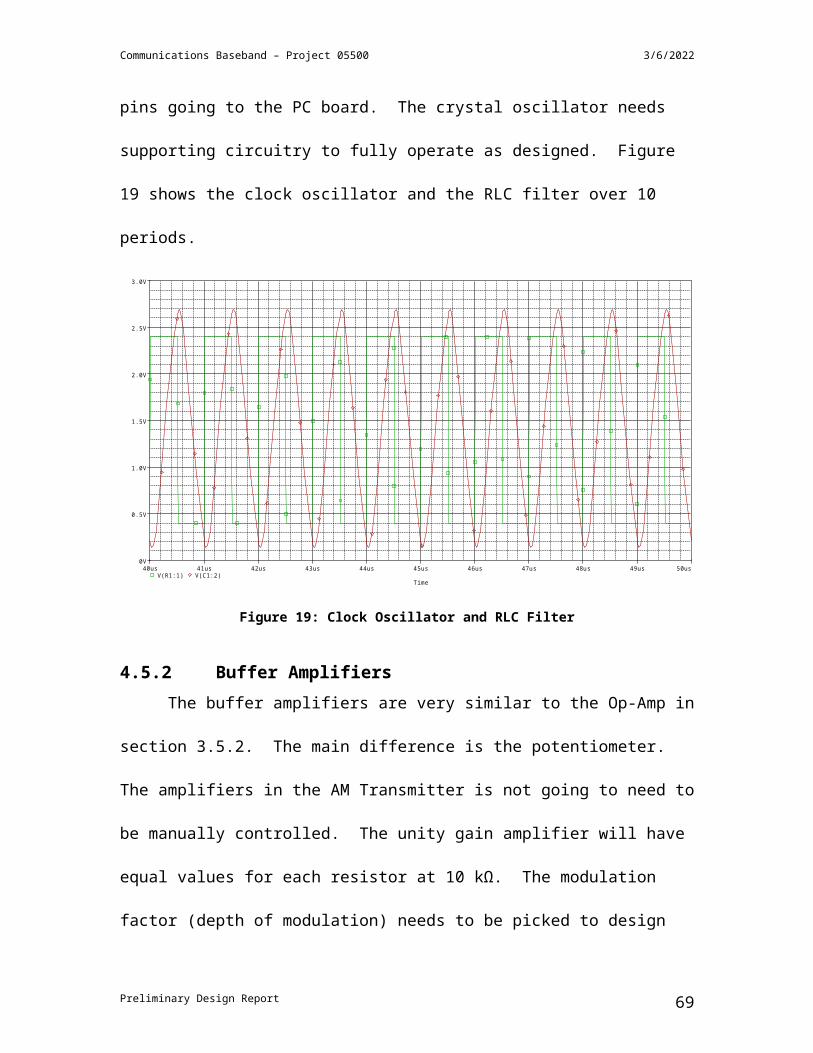
Communications Baseband – Project 05500 5/8/2023
Figure 30 - Quantization of an analog signal into L levels
The voltage levels are designated by horizontal cross sections; the samples are
represented by the vertical lines that intersect the signal. Clearly the sampled voltages
may not correspond to a specific voltage level (Vss+Vpp/L*n; where n is quantization
level) in the quantization. Therefore some rounding must occur. The more levels there are
the more accurate each sample will be since there will be less rounding error.
After each sample is correlated to each nearest voltage level, L, a corresponding
binary word representation is assigned. The lowest voltage value is given by 0 binary and
the highest voltage value (Vdd) as 2^L in binary. To represent L voltage levels it requires
n = log2 L bits. Therefore the higher the sample size the better resolution of the sample.
Quantization noise is the error caused by rounding. The signal to noise ratio in dB for an
n-bit sample of the quantization process is given by,
Preliminary Design Report 69
Communications Baseband – Project 05500 5/8/2023
This shows that each additional bit increases the SNR by 6dB. The tradeoff in having a
higher resolution AD converter is the need for a higher bandwidth.
PCM Encoding Format
It is known that PCM encoding results in a bit stream of n-bit samples, however, the
format is important. There are many PCM waveform schemes such as NRZ, RZ,
unipolar-NRZ, etc. Typical AD converters output a signal where a binary ‘1’ in the bit
stream corresponds to the highest voltage supplied to the chip, Vdd, and a binary ‘0’
corresponds to a voltage low, Vss, which is typically –Vdd or 0V. This PCM waveform is
known as NRZ-L.
The PCM waveform is very important to the design because it determines the bit
rate necessary of the system, the ability to transmit the signal wirelessly, and the type of
modulation used to transmit the signal over RF. The PCM waveform also will affect the
bandwidth and the shape of the frequency spectrum of the signal.
Other important factors in PCM encoding are the resolution and throughput. The
resolution defines how many bits per sample are taken and the throughput defines the
data rate for which the samples should be sent out of the system. Both factors affect your
required transmission bandwidth, given by , where B is the bandwidth required
of the RF system, n is the resolution of the PCM signal, and f is the sampling frequency.
Digital to Analog Conversion
On the receive side the process of converting each digital PCM code sample must
be reversed. A digital to analog converter takes each n-bit sample and converts it into the
corresponding voltage, Vout = Vss+Vpp/L*n; where n is the quantization level. After this
Preliminary Design Report 70
Communications Baseband – Project 05500 5/8/2023
stage a low pass filter should be employed to cut out any higher frequencies than the
message signal contains.
7.2.2 Choosing ComponentsMicroprocessor
The components for this system were initially chosen on the basis of design
requirements. It was decided first that a PICmicro microcontroller would be used to
provide AD conversion. This decision was based on the AD capability, the required
sample rate being met, the cost, and the availability. Also it was thought some encoding
format would be applied by the PIC, until it was decided to go with the standard NRZ-L
that does not require any processing. The initial design parameters that modeled the
component decision are shown below in Table 18.
PCM System Design ParametersDesign Parameter Importance DesireabilitySupport 20kHz audio 1 9Support 4kHz voice quality audio 10 10AD Resolution 8 8Provide Data Flow Control 10 10Low Bandwidth 10 7Cheap 9 10
Table 18 - Design Parameters for PCM System
The team leader pushed the importance of supporting 20 kHz audio in order to
make the system capable of transmitting any standard audio signal. The PIC16F870 was
the initial processor choice and provides a 10-bit AD converter with a maximum clock
speed of 20MHz. The AD converter on the PIC has a sample and hold circuit that can
sample up to 50.7 kHz therefore the desired 44.1 kHz sample rate can be achieved. The
PIC takes a maximum of 4 clock cycles to perform an instruction, therefore the 20 MHz
clock is cut in four and each instructions maximum execution frequency is 5 MHz.
Preliminary Design Report 71
Communications Baseband – Project 05500 5/8/2023
Initially this frequency was thought to be plenty of time to perform instructions. The
different options for bandwidth are summarized below in Table 19.
Bandwidth Options
OptionAudio Bandwidth
AD Resolution
Sample Frequency
Bandwidth Required
Least 4kHz 8-bit 8kHz >64 kbpsReasonable 16 kHz 10-bit 32 kHz >320 kbpsDesired 20 kHz 10-bit 44 kHz >440 kbps
Table 19 - Bandwidth Choices
Digital to Analog Converter
The other component required in this system is the digital to analog converter. A
Digital to Analog Converter (DAC) is necessary to return the 10-bit PCM signal
produced by the PIC16F870 and transmitted via the GFSK transceiver back into a
continuous voltage signal. The FSK chip sends out pure data then some additional header
information that is used for asynchronous transmission. The PIC will strip off any header
information and pass through 10 bits at a time to the DAC at precisely the sampling rate
(~22µs) using a USART.
Because the PIC only has about 15 I/O pins serial transmission is desired from the
PIC to the DAC. Also the DAC requires a clock and some control lines.
Options
Using the specifications above, two DACs were found to meet these needs, one from
Analog Devices and one made by Texas Instruments. Both DACs will do the job, but
some considerations were taken to decide upon which to use as shown in Table 20.
Texas Instruments Analog DevicesVdd=3.3V No (-1) Yes (+1)Cheaper Yes (+1) No (-1)Requires Overhead bits Yes (-1) No (+1)Integral Nonlinearity +/-1 LSB +/-1.75 LSBDifferential Nonlinearity +/-0.5 LSB +/-0.9 LSBTable 20 - DAC Options
Preliminary Design Report 72
Communications Baseband – Project 05500 5/8/2023
The Analog Devices chip is the most desired of the two because it requires no
overhead bits. The TI DAC requires 2 overhead bits per sample. This will require
additional programming and is not desirable.
There are several PIC chips investigated. Aside from the sampling and clock
performance, the PIC was chosen based on the following parameters:
DIP for ease of making the circuit
Amount of Pins
Clock speed
RAM and Program Memory
The key parameters are listed below in Table 21.
PIC Options
PriceProg Memory
Data Memory EEPROM
Max Speed I/O Package
PIC16F870 $2.81 2k X 14 128 bytes 64 bytes 20 MHz 22 28-DIPPIC18F1320 $3.15 4096x16 256 bytes 256 bytes 40 MHz 16 18-DIPPIC18C242 $5.12 8192x16 768 bytes 0 40 MHz 23 28-DIPPIC18C252 $5.57 16384x16 1536 bytes 0 40 MHz 23 28-DIP
Table 21 - PIC Options
The PIC18C series are the choice options since they have a higher clock speed,
greater program and data memory as well as more interfaces (serial, USART, PC).
7.3 Feasibility AssessmentThe feasibility of this portion of the project relies on the ability to choose design
performance parameters that are capable of being processed by prepackaged equipment,
specifically the equipment that has been chosen. The feasibility is based on the following
design parameters:
Sample Rate
AD Resolution (Sample Size)
Preliminary Design Report 73
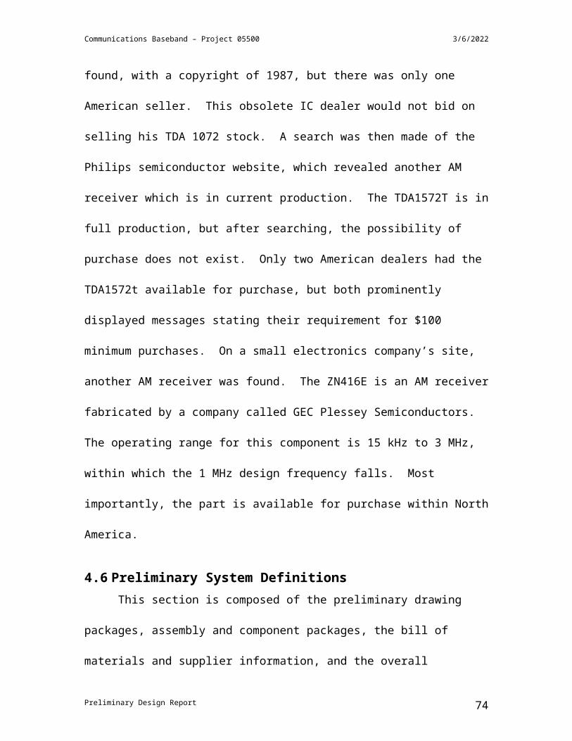
Communications Baseband – Project 05500 5/8/2023
PIC microcontroller clock speed
PIC program size
Transmission protocol
The electronics to provide these functions have been found and apparently meet our
desired specifications. The last two design parameters are yet to be experimented with
and are left for Senior Design II. As established in Section 7.2.2, there are several options
to choose in order to meet the specifications. So far the plan is to use a PIC and a Analog
Devices DAC.
The work load for senior design I and Senior Design II can be broken down as
shown in Table 22.
Time Dedication TableSD I SD II
PIC Research 50 20PIC Programming 0 80System Specs 20 20Team meetings/coordination 30 20
Table 22 - Work Load Breakdown Winter/Spring (Hrs)
So far the options investigated seem to be very possible to implement by May 2005
and therefore the portion to implement PCM encoding and transmission flow is feasible.
7.4 Design ObjectivesThe first thing to choose is the resolution and throughput as defined in section 7.2.1.
The PICmicro microcontroller on-board AD converter has a resolution of 10-bits. The
sampling rate desired is 44 kHz. The PIC will have to be programmed to control the AD
conversion and control the FSK chip.
7.4.1 Performance SpecificationsThe following definitions of the PIC and DAC specifications have been given:
Preliminary Design Report 74
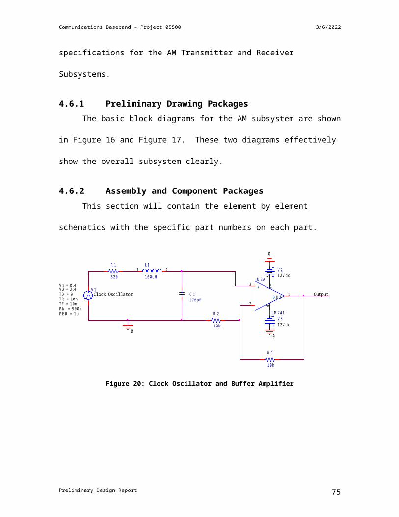
Communications Baseband – Project 05500 5/8/2023
1) The PIC must deliver data to the FSK chip at 1Mbps.
2) The PIC must send out each 10 bit data packet at exactly the initial sample rate
(~44.1kHz) to the DAC.
3) The operating voltage is 3.3V, the digital signal will be sent rail-to-rail VDD.
4) DAC should run off 3.3V
5) The data will be sent serially.
6) A clock signal at the data rate must be sent to the DAC by the PIC.
The options provided in section 7.2.2, Table 20 - DAC Options and Table 21 - PIC
Options show the different options available, which all meet the above specs.
7.4.2 Implementation SpecificationsThe PIC must be programmed to perform the tasks listed above. The PIC must do
the following:
Perform AD conversion at specific rate
Transmit data to FSK chip
Receive data from FSK chip
Send data out to DAC
The first two are required for the transmit side PIC and the last two are for the receive
side PIC. A block diagram of the transmit PIC program flow chart is shown below in
Figure 31.
Preliminary Design Report 75
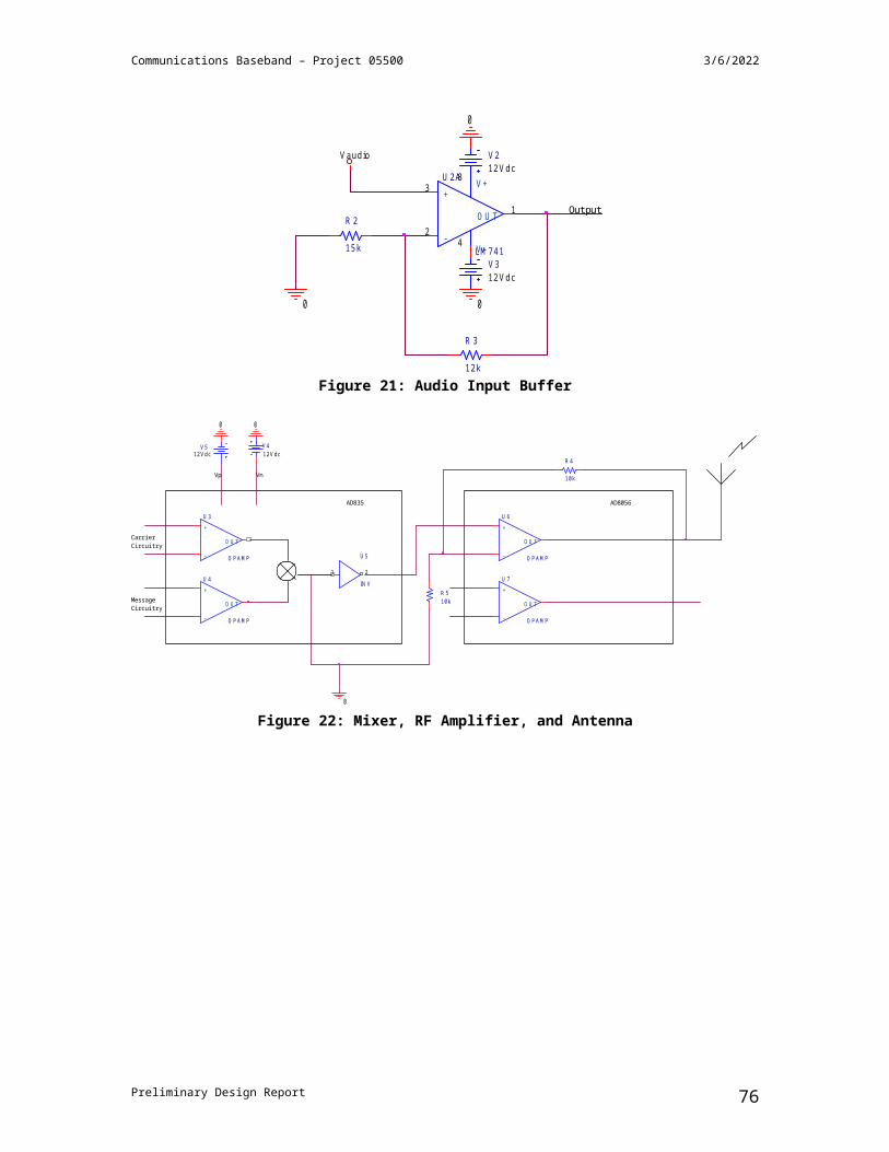
Communications Baseband – Project 05500 5/8/2023
Figure 31 - PIC Transmit Side Program Flow Chart
The flow chart for the receive side PIC program is shown below in Figure 32.
Preliminary Design Report 76
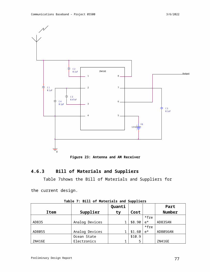
Communications Baseband – Project 05500 5/8/2023
Figure 32 - Receive side PIC program flow chart
The flow charts for the receive and transmit side consider the implementation of all
processes necessary to encode the data, send across an RF link, and send the data to be
decoded by a DAC. Therefore the design has satisfied all requirements.
7.5 Design SynthesisSeveral concerns exist as to how well the PIC16F870 that was initially chosen will
meet the specifications of this project. The concerns affecting the feasibility of the PIC
being appropriate are:
Preliminary Design Report 77
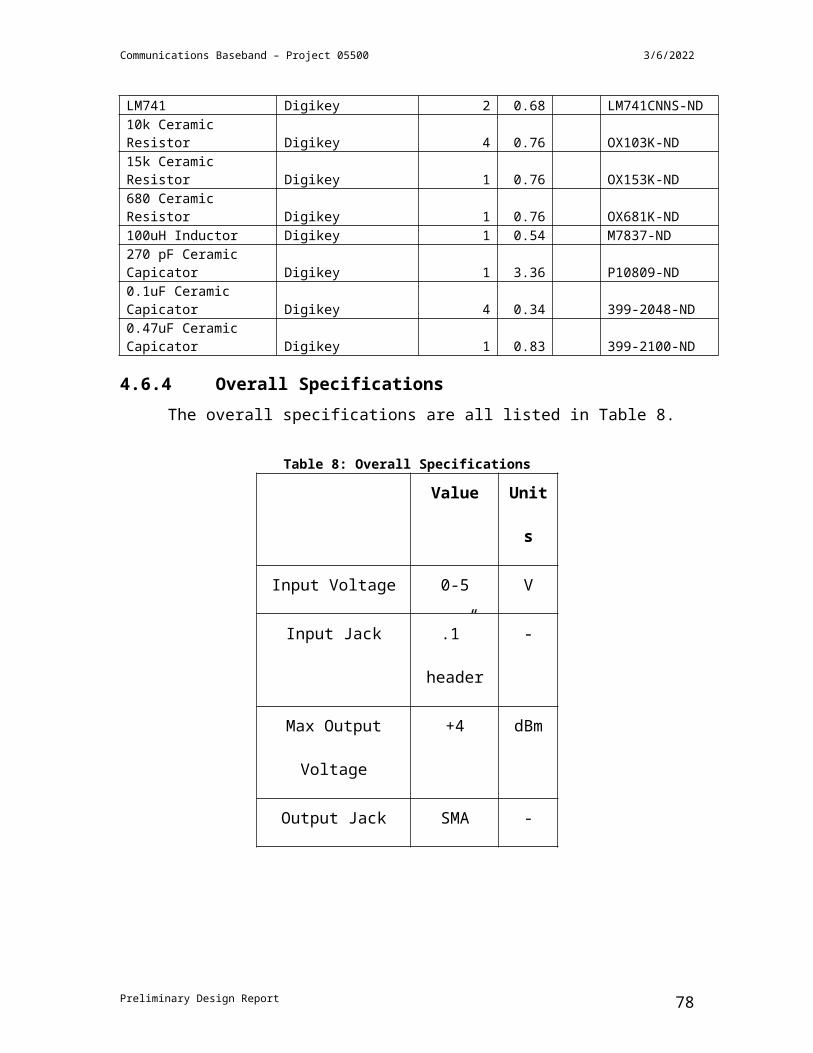
Communications Baseband – Project 05500 5/8/2023
Sample at a precise rate
Sending exactly 1 Mbps of data from USART to FSK chip
Managing data transmission with an 8-bit USART and 10 bit audio samples
Sending the data from PIC to DAC at precisely the sample rate
Sending a clock to the DAC at the precisely the sample rate
The ability to perform 44 kHz sampling and have time to perform the other
operations
Some of the concerns listed above are simply a matter gaining experience with the
PIC and knowing it will do what it says it can do. The other portion is the details in
integrating the specifications for one component to another component. With digital data,
especially at high data rates, specifications have very little allowance for error. The only
portion of the project that experiences the precise transfer of digital data is between the
microprocessor and the FSK chip. This link is imperative to system performance and
therefore must be methodically engineered.
USART
The USART (Universal Synchronous Asynchronous Receiver Transmitter) can
offer the capability of transmitting and receiving data at a specified clock rate. The
USART on the PIC sends out 8-bits at a time at the rate of some multiple of the clock
frequency. The baud rate is given by the following formula:
Preliminary Design Report 78
Communications Baseband – Project 05500 5/8/2023
Where Fosc is the system clock, X is an integer from 0 to 255, stored in the SPBRG
register. It is not possible to achieve a 1MHz baud rate with the 20 MHz PIC. No integer
value of X provides a baud rate of exactly 1 MHz. The PIC18C series can handle up to 40
MHz clock operation as shown in Table 21 - PIC Options. For the PIC18C, a 32 MHz
crystal can be used to generate the clock, and the SPBRG register in the PIC can be set to
1 resulting in a baud rate of exactly 1 Mbps.
The USART transmits 8 bits at one time. In Asynchronous mode the 8 bit data is
padded by a start and stop bitData can be transmitted back to back by placing the next 8
bits into TXREG after the start bit is sent, when the stop bit is transmitted it will load that
register into the TSR register for transmission.
7.5.1 Digital Transmission ProtocolThe current condition is that the transmit protocol which will satisfy the
specifications best is uncertain. The two options are synchronous and asynchronous
transmission. The FSK chip has two modes, Shockburst and Direct mode. Shockburst
mode requires a clock and is thus synchronous. Direct mode does not require a clock but
requires an exact data rate of 1 Mbps transfer to the chip. Some options investigated with
these two modes will be discussed next.
Synchronous Transmission
The initial assumed method of transmission is shown below in Figure 33. It was
assumed that synchronous transmission would provide the best data rate since there are
no overhead bits. The FSK chip must be in Shockburst mode for synchronous
transmission and is shown in the figure. In this mode a bit stream of up to 230 bits can be
sent at up to 1Mbps. The chip clocks in the data, and then transmits at 1Mbps. The figure
Preliminary Design Report 79
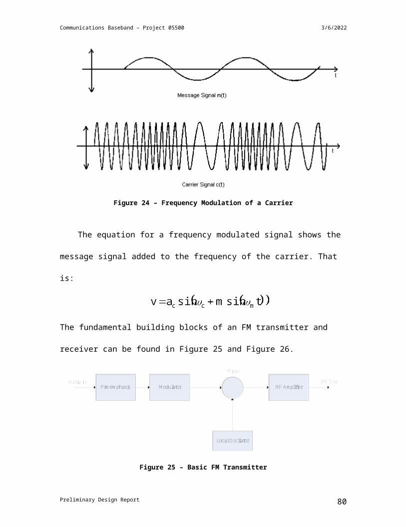
Communications Baseband – Project 05500 5/8/2023
shows this method is not possible if the sampling rate of 44 kHz is to be satisfied. In this
mode, using the packet size of 20 samples, the figure reveals a sample rate of 31 kHz
would be necessary. This does not satisfy the desired specifications therefore some other
options were investigated.
Figure 33 - Timing Diagram for FSK Chip in Shockburst Mode
The PIC must send information out as fast as it samples. Therefore the time it takes
for the packets to send out to the FSK chip must be within a small integer multiple of the
sampling time. That small integer number is how many samples will have to be
temporarily stored in PIC memory.
Asynchronous Transmission
The other method of transmitting with the FSK chip is using Direct mode. In this
mode data must be constantly clocked in at 1Mbps precisely – within 200ppm (parts-per-
million). No clock is required. In this mode data is started by sending an 8 bit preamble
and ended by sending another word, or sending no data for a while. One option for
sending in this mode is shown below in Figure 34.
Preliminary Design Report 80
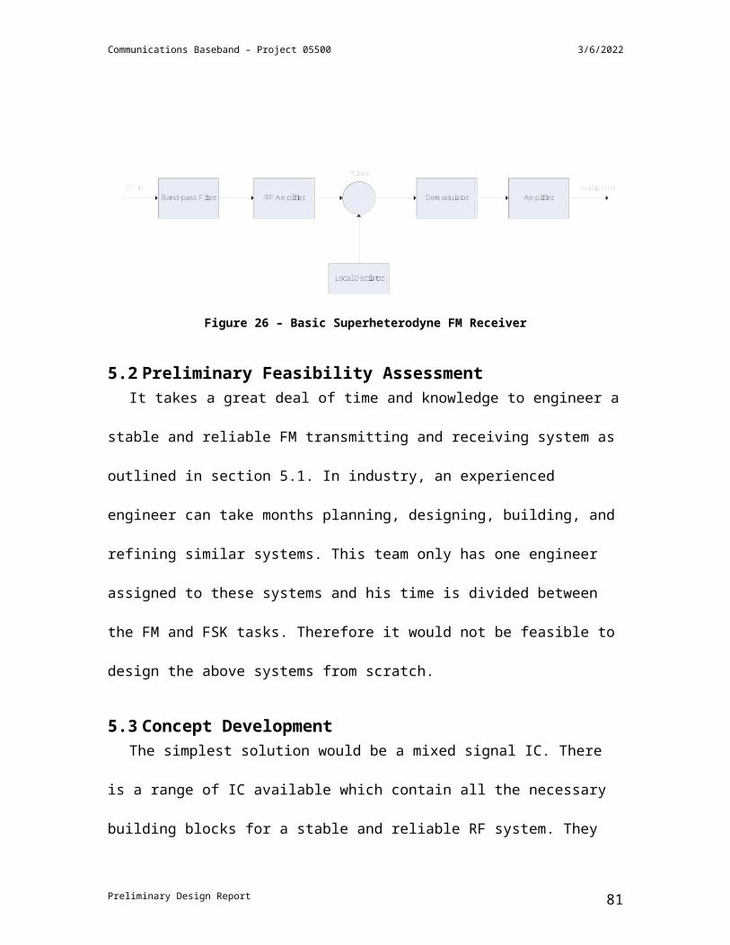
Communications Baseband – Project 05500 5/8/2023
Figure 34 - Asynchronous Data Transmission – 2 Samples
In this figure two 10-bit samples are sent one after another however 8-bit words must be
sent therefore 4 bits of non-data must be added to the 4 trailing data bits. Using this
method the sample rate must be 33.3 kHz. This still does not meet the desired
specification.
Another option is shown in Figure 35. Here 1 sample is transmitted in two words.
The second word contains only 2 data bits therefore must have 6 non-data bits.
Figure 35 - Asynchronous Data Transmission - 1 Sample
With this format a sampling frequency of 50 kHz is required. This meets the desired
specification and is even better. It is certain no aliasing problems will occur with the
desired input frequency range of 20 kHz.
The table below summarizes the different options shown above.
Preliminary Design Report 81

Communications Baseband – Project 05500 5/8/2023
FSK Chip Mode Frame Size Necessary Sample Rate Memory Shockburst 20 samples 31 kHz 200 bytesDirect 2 samples 33.3 kHz 2 bytesDirect 1 sample 50 kHz 1 byte
Table 23 - Digital Transfer Protocol Options
The ideal method at this point is the asynchronous mode 1 sample providing a
sampling rate of 50 kHz.
System Synchronization
An important part of any digital communications system is synchronization. Every
system must have the same clock time. In this system the FSK chip serves as a break in
the connection between the send and receive PIC because it has its own clocking system.
Therefore it is not necessary to manually provide simultaneous clocks on the transmit and
receive side. This is very convenient. All that is necessary on the receive side is for the
PIC to be prepared to start accepting data at 1 Mbps when the FSK chip starts sending it.
7.6 Preliminary System DefinitionThe schematic pin to pin interface between the PIC and the FSK chip is shown
below in . This shows the pins necessary for the input data and connection to the FSK
chip.
Preliminary Design Report 82
Communications Baseband – Project 05500 5/8/2023
Figure 36 - Transmit Side Pin to Pin PIC-FSK Connections
The receiver side schematic is shown in Figure 37.
Figure 37 - Receiver Side Pin to Pin PIC-FSK-DAC Connections
A list of the pin definitions so far used for the PIC is given below.
Pin 2 - RA0/AN0 – Analog input for transmit side. Input voltage should remain at (Vss – Vdd). Pin 3 – RA1/AN1 – Digital Input for synchronous data (future addition)Pin 8 – VSS – Circuit ground (common = 0V).Pin 9 – OSC1/CLKIN – Connected to crystal and 16pF capacitor to provide the clockPin 10 – OSC2/CLKOUT – connected to other side of crystal
Preliminary Design Report 83
Communications Baseband – Project 05500 5/8/2023
Pin 17 – RC6/TX – USART TX for synchronous data transmission to FSK chipPin 18 – RC7/RX – USART RX for digital reception on receive side from FSK chip.Pin 20 – VDD – This is the positive power supply. Since the FSK chip uses 3.3V, this will be used for the PIC so that the digital data out has a 0V-3.3V range. Pin 19 - VSS – Circuit ground (common = 0V).
Budget and Parts List
The initial parts list is shown below in Table 24.
Quantity Description MFG Suppliers P/N Supplier Price2 CAP 15PF 100V CERAMIC MONO 5% EPCOS Inc 495-1002-1-ND Digikey 0.162 CRYSTAL 20.0000MHZ 18PF CYL Epson SE3438-ND Digikey 0.962 IC MCU FLASH 2KX14 EE 28DIP Microchip PIC16F870-I/SP-ND Digikey 4.80
1 IC 10 BIT 12.5US DAC S/O 8-DIPTexas Instruments 296-3006-5-ND Digikey
Table 24 - Preliminary Parts List
This parts list is outdated as per the discussion in 7.5. The final parts will be known
once a working communications protocol is chosen.
Future Goals
The future of the digital control and transmission portion of the project relies
selecting the sample rate desired and determining if the PIC can actually implement the
necessary program in time. Ultimately the PIC program will have to be implemented and
tested to see if the data is clocking through as expected.
Preliminary Design Report 84
Communications Baseband – Project 05500 5/8/2023
8 Current Design This section outlines the project as it currently stands. The system and its parts have
been developed and discussed in detail in the proceeding sections. Very little discussion
will be done here.
8.1 System Definition
Figure 38 – Current System Block Diagram
Preliminary Design Report 85

Communications Baseband – Project 05500 5/8/2023
8.2 Target System Specifications
8.2.1 RF performanceRF performance is specific to each individual subsystem and will be discussed in
the respective sections. The only system requirement is that a reliable wireless link is
established across a classroom.
Parameter SpecificationMinimum Range 10mMax BER at min Range 0.1%Output Impedance 50ohm
Table 25 – RF Specifications
8.2.2 PackagingSystem should be enclosed to prevent physical or electrical shock due to touching.
Packaging will be constructed from raw materials once the subsystems are together
and working. This will most likely consists of the discrete boards mounted to an
aluminum base. The base will be grounded and the individual boards will be
separated by conducting walls for shielding purposes if RFI problems present
themselves. The unit will have a see-through cover so that students can see the inner
workings.
External SMA RF connectors will be provided for each of the three modulation
schemes. These will be used for the purpose of connecting to a spectrum analyzer for
viewing.
8.2.3 EnvironmentalMost of the components in the system will be rated for use in the
temperature range from -45°C to +85°C. However the unit will not be tested for
operation at those extreme temperatures and therefore is not recommended. The
recommended temperature range is that of a lab environment.
Preliminary Design Report 86
Communications Baseband – Project 05500 5/8/2023
Parameter Operating RangeTemperature 25°C +/-20°CHumidity Any, as long as no condensation is forming.
Table 26 – Environmental Specifications
8.3 Preliminary Budget AnalysisThis section discuses initial cost projections for the deign project.
Item Price ($)Board Layout 100FM Transmitter Parts 40FM Receiver Parts 30GFSK Transceiver Parts 30Audio Section parts 25AM Receiver Parts 30AM Transmitter Parts 30PIC Implementations 15Power Supply 15RF Cables 30Misc. Prototype Materials 20Total 365
Table 27 - Budget Analysis
A board layout is planned for the GFSK Transverse, FM Receiver, and FM
Transmitter. These three separate boards will be combined into a single board layout that
will cost a minimum of $51 and as much as $100 from ExpressPCB.com depending on
how much space the individual layouts consume.
The GFSK, FM modulator, and FM demodulator are all well defined at this point
and already have schematics and parts lists. Therefore, this analysis should to be accurate
within $50. However, there are a large amount of parts and materials which are available
from the Electrical Engineering free of charge. This means the actual cost of the project
could be much lower then projected.
Preliminary Design Report 87
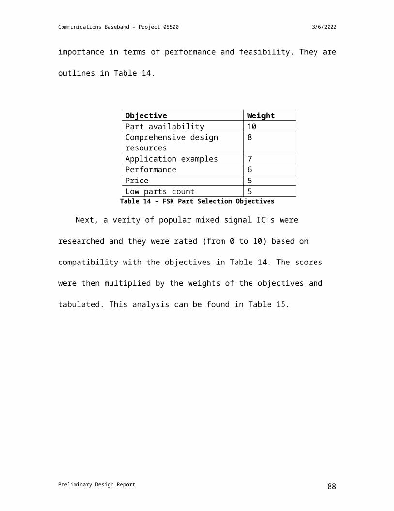
Communications Baseband – Project 05500 5/8/2023
9 Project OutlookAt this point it is half way through the deadline time. The projects individual
subsystems have been investigated and developed. Schematics have been made for
several of the components and all parts have been decided upon. The development and
understanding of operation of each subsystem is satisfactory enough to be able to
implement the systems in hardware. The customers wanted simulations of the project and
those should be completed after the break. The parts lists still need to be compiled in
order to have parts ordered before the Spring break.
9.1 Senior Design I – Winter QuarterA week by week analysis of the tasks that should be completed for Winter quarter
was made is shown below.
Senior Design I Timeline
Project 05500 – Communications Baseband
Week 1 – December 3
Leland made up project outline with Dr Delorenzo. The goal is to build some
communication system to demonstrate as a lab for the 354 class Intro to
Communications. The project should have AM, FM, and utilize PCM.
Week 2 – December 10
Preliminary Design Report 88

Communications Baseband – Project 05500 5/8/2023
Leland persuaded Jason Riesbeck and Jonathan Hutton to join the project. We had
our first meeting and assigned team members a portion of the project based on their
experience level and interest. Found books for research at the library. Set up meeting with
project advisor.
Week 3 – December 17
Specified block diagram of entire project. We narrowed down components and
technology to use and assigned team members to each portion for research over break.
This is discussed in the Team document.
Week 4 – January 7
Report all research done. Made refinements to system block diagram and refined
feasible implementations based on components chosen.
Week 5 – January 14
Research and components chosen for each block, either design with sources of
design or bought.
Week 6 - January 21
Met with Dr. Delorenzo to discuss system diagram and practicality of component
choices.
Preliminary Design Report 89
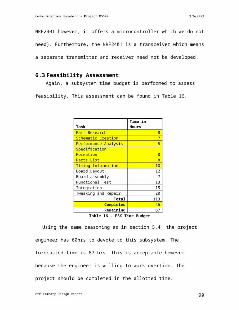
Communications Baseband – Project 05500 5/8/2023
Week 7 – January 28
Leland: Must have schematic and parts list for PIC to build interface board for
AD, DA, input and output, with clocks etc. Must have solution for companding
(compression/expansion). Understand PIC DA/AD.
Jason: Have chosen FM, FSK transmitters. Provide specification documents for
required inputs (voltage levels or dB, sensitivity etc), required circuitry for operation
(power supply voltages/power, external circuitry), and the output of each chip (voltage
levels, etc).
Jon: Have many datasheets/specs/prices for input line amplifier, LPF (20khz),
compression chips/circuitry, 2.4GHz antenna’s. Look into some low power amplifiers for
transmit and receive (Jason says we may not need to amplify, note Jason our path loss
will be a reduction of a factor of 60dB (so if we put out 1mW then that’s -90dBW=-
60dBm at receiver). Have detailed block diagram of AM transmission system, all
components from microphone to speaker. Research those components.
All: Documents (should have at least 3) describing each process must be made,
starting with goals, discussing procedure/methodology and describe conclusions/results.
Print all datasheets that we will use and related any material that aided your design
process and decisions. This important from now to the end of the quarter – write all
research down typed!!!
Preliminary Design Report 90
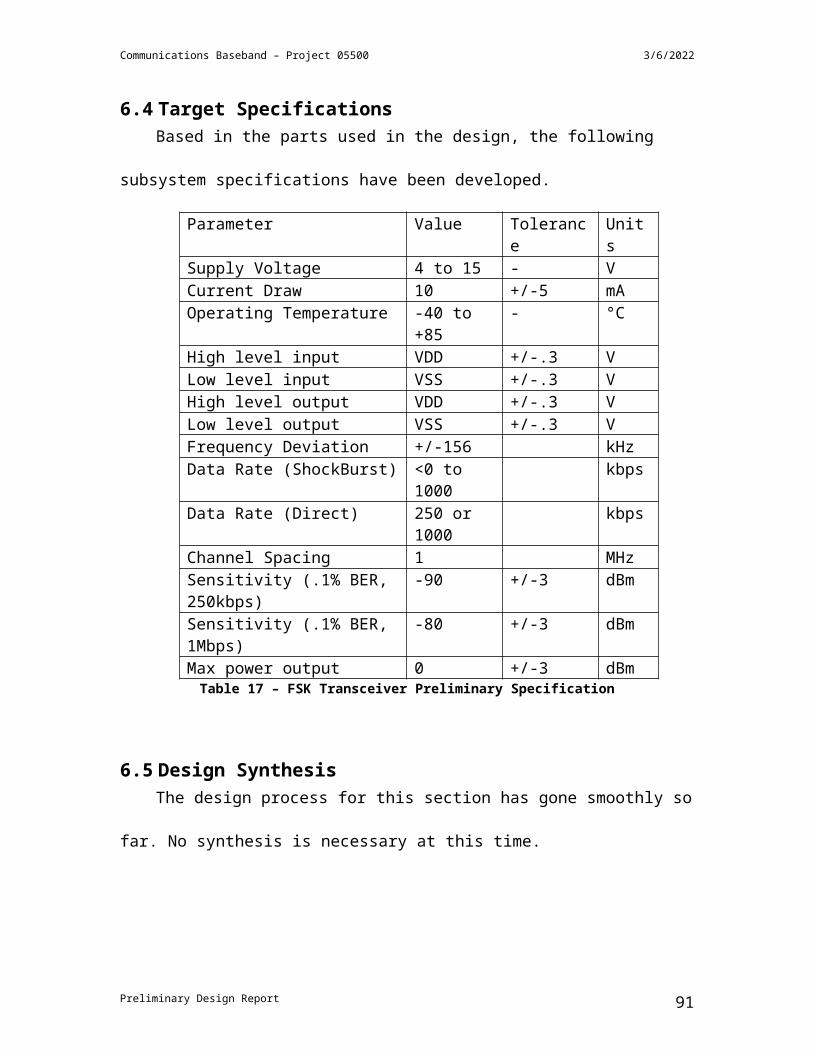
Communications Baseband – Project 05500 5/8/2023
We will meet mid-week to prepare for peer design review. Need write up of project
operation and goals, understand each part of the system to describe our process.
Peer design review!
Week 8 – February 4
Should have schematics for most of project. Should have write ups on all parts of
the project describing in detail our performance goals, input/outputs, specs, design
procedure, choice in products and prices. This date is the goal for having selected all the
components in the system. We should have a complete block diagram of signal path with
all portions researched and implementation known. We should begin simulations of each
portion of the project in Matlab.
Look into requirements for PDR write up. We will divide up the PDR’s
requirements into 3 and each of us will compile and add as necessary information and BS
to the sections we choose.
Week 9 – February 11
All schematics complete. Whole system designed. Simulation near completion.
Begin to compile all simulations, schematics, and random documents, graphs, everything
and throw it into the PDR file which should have a complete table of contents by now
Preliminary Design Report 91
Communications Baseband – Project 05500 5/8/2023
and sections typed up. So we can drop our files etc into this doc and start organizing it
and typing all the nice descriptions.
Week 10 – February 18
Must have PDR completed, printed up nicely and bound at Hub.
Practice Final Design review in front of Advisor and Paul Garsin. Have
powerpoint presentation – each of us will go over ‘our’ portion of the design project and
come up with our own presentation or idea of what to say. We should have handouts for
the review committee – a summary of project, its design goals, briefly how we
implemented it, and our expectations (simulations).
9.2 Senior Design II - Spring QuarterThe plan for Senior Design II is to get started building components right away. It is
understood that things never work out as planned and thus the plan is to complete things
ahead of time so there is time for troubleshooting. A detailed chart of the work timeline is
shown below on Page 93.
Preliminary Design Report 92
Communications Baseband – Project 05500 5/8/2023
Preliminary Design Report 93
Seni
or D
esig
n II
Wor
k Ti
mel
ine
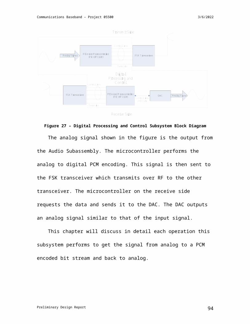
Communications Baseband – Project 05500 5/8/2023
9.3 Beyond SDIIThis project is made for a communications lab therefore it will be used in the future
by new professors and students. The manual provided along with the other deliverables
will discuss how to maintain the project and list all the specifications. The nice thing
about this project is that it is upgradeable. Because all the subsystems are individual
working systems, they can be either removed or replaced. Often time professors want to
show how a communication system is disrupted by noise or other external devices. It
would be possible to simply connect in some additional attenuation or noise to show how
it affects the spectrum of the signal. Additionally, the microprocessor allows the ability to
apply formatting to the digital data. This is a very important aspect of digital
communications. Encoding data will affect the spectrum in different ways. Because the
microprocessor handles all this data, it would be simple to add data this additional
functionality.
Preliminary Design Report 94
Communications Baseband – Project 05500 5/8/2023
Appendix A – References
“RS232 Specifications and standard”, Lammert Bies. (http://www.lammertbies.nl/comm/info/RS-232_specs.html)
“What is USB?”, bugclub.org. (http://bugclub.org/beginners/hardware/usb.html)
“Telecommunication - Operation within the bands 902-928 MHz, 2400-2483.5 MHz, and 5725-5850 MHz.” TITLE 47, CHAPTER I, PART 15, Subpart C, Sec. 15.247; FEDERAL COMMUNICATIONS COMMISSION (http://www.access.gpo.gov/nara/cfr/waisidx_03/47cfr15_03.html)
“United States Frequency Allocations ‘The Radio Spectrum’” October 2003, U.S. Department of Commerce, National Telecommunications and Information Administration, Office of spectrum Management (http://www.ntia.doc.gov/osmhome/allochrt.pdf)
“Unlicensed Frequencies“, zytrax.com (http://www.zytrax.com/tech/wireless/free.htm)
NRF2401 Data Sheet: “Single Chip 2.4 GHZ Transceiver”, Rev. 1.1, Nordic Semiconductor
NAN24-05 Application Note: “nRF24e1 Wireless Hand-Free Demo” , Rev. 1.2, Nordic Semiconductor
NAN24-04 Application Note: “Universal Low Cost USB DuoCeiver Using an nRF2401” , Rev. 1.0, Nordic Semiconductor
NAN400-07 Application Note: “nRF Radio Protocol Guidelines” , Rev. 1.2, Nordic Semiconductor
Design of Analog Filters, Rolf Schaumann and Mac E. Van Valkenburg, Oxford University Press.
Modulation, 2nd edition. F R Connor, Thomson Litho Limited.
Electronic Communications Modulation and Transmission, 2nd edition. Robert Schoenbeck, Macmillian Publishing Company.
Digital Communications Fundamentals and Applications, 2 nd edition, Sklar
Preliminary Design Report 95
Communications Baseband – Project 05500 5/8/2023
Appendix B – Design Documents
Preliminary Design Report 96

Communications Baseband – Project 05500 5/8/2023
Choosing a DAC Leland Smith2/10/05
A Digital to Analog Converter (DAC) is necessary to return the PCM 10-bit signal produced by the PIC16F870 and transmitted via the GFSK modem back into a continuous voltage signal. The FSK chip sends out pure data then some additional header information that is used for asynchronous transmission. The PIC will strip off any header information and pass through 10 bits at a time to the DAC at precisely the sampling rate (~22µs). The following definitions of the PIC digital output and DAC specifications have been decided upon:
7) The PIC must send out each 10 bit data packet at exactly the initial sample rate (~44.1kHz). Some DACs require some header bits for processing time.
8) The operating voltage of the PIC is 3.3V therefore the digital signal will be sent rail-to-rail VDD.
9) DAC should run off 3.3V10) The data will be sent serially.11) A clock signal at the data rate must be sent to the DAC by the PIC.12) The package must be a DIP.
Because the PIC only has about 15 I/O pins serial transmission is desired from the PIC to the DAC. Also the DAC requires a clock and some control lines.
Using the specifications above, two DACs were found to meet our needs, one from Analog Devices and one made by Texas Instruments. The Digikey.com ordering information for each of these is below.
1) Analog Devices 10bit DAC
Digi-Key Part Number AD7391AN-ND Price Break 12510025050010005000
Unit Price 7.220005.776004.873504.693004.584704.512504.40420
Price7.22
144.40487.35
1173.252292.354512.50
22021.00
Manufacturer Part Number AD7391AN
Description IC DAC 10BIT SRL 3V 8-DIP
Quantity Available 1
Technical/Catalog Information AD7391AN-ND
Standard Package 100
Category Integrated Circuits (IC's)
Family D/A Converters (D-A)
Vendor Analog Devices Inc
Preliminary Design Report 97

Communications Baseband – Project 05500 5/8/2023
2) Texas Instruments 10-bit DAC
Digi-Key Part Number 296-3006-5-ND Price Break 12510025050010005000
Unit Price 4.070003.258002.534002.407322.353002.307752.26250
Price4.07
81.45253.40601.83
1176.502307.75
11312.50
Manufacturer Part Number TLC5615CP
Description IC 10 BIT 12.5US DAC S/O 8-DIP
Quantity Available 1139
Technical/Catalog Information 296-3006-5-ND
Standard Package 50
Category Integrated Circuits (IC's)
Family D/A Converters (D-A)
Vendor Texas Instruments
Number of Bits 10
Package / Case 8-DIP
Features Low Power
Data Interface Serial
Packaging Tube
Other Names 296-3006-5
Both DACs will do the job, but some considerations were taken to decide upon which to use.
Texas Instruments Analog DevicesVdd=3.3V No (-1) Yes (+1)Cheaper Yes (+1) No (-1)Requires Overhead bits Yes (-1) No (+1)Integral Nonlinearity +/-1 LSB +/-1.75 LSBDifferential Nonlinearity +/-0.5 LSB +/-0.9 LSB
Preliminary Design Report 98

Communications Baseband – Project 05500 5/8/2023
Logarithmic AmplifierLeland Smith1/20/05
The PIC will PCM encode an analog input with a dynamic range of 5V. It has a 10 bit encoder; therefore there are 1028 levels of quantization. Considering the input maximum is 5V from our amplifier the quantization level is 5mV. This may or may not be satisfactory. If say the max voltage is 1V from the microphone there will be a lot of quantization noise. The logarithmic amplifier will amplify lower signals greater than higher signals, thus weak audio signals will be amplified more than large signals. A graph is shown below. The logarithmic amp before a 12bit AD converter can create a dynamic
range to that of a 20bit AD converter.
Preliminary Design Report 99
0 0.5 1 1.5 2 2.5 3 3.5 4 4.5 5-5
-4
-3
-2
-1
0
1
2
Voltage
Gai
n
Logarithmic Amplifier Vout/Vin
Communications Baseband – Project 05500 5/8/2023
PICmicro Microcontroller Specifications
Leland SmithDate: 1/16/05
Scope: This document’s purpose is to provide information regarding the PIC microchip used to implement the A/D, PCM, and digital encoding portion of the project.
In order to PCM encode our team initially chose to use the PIC16F870 because Jason Riesbeck had one on hand. A summary of the PIC is on the website1A www.microchip.com and is quoted below:
Summary: This powerful (200 nanosecond instruction execution) yet easy-to-program (only 35 single word instructions) CMOS FLASH-based 8-bit microcontroller packs Microchip's powerful PIC® architecture into an 28-pin package and is upwards compatible with the PIC16C5X, PIC12CXXX and PIC16C7X devices. The PIC16F870 features 64 bytes of EEPROM data memory, self programming, an ICD, 5 channels of 10-bit Analog-to-Digital (A/D) converter, 2 additional timers, a capture/compare/PWM functions and a Universal Asynchronous Receiver Transmitter (USART). All of these features make it ideal for more advanced level A/D applications in automotive, industrial, appliances and consumer applications.
Some other features are:
Budgetary Price Memory Type Bytes Words
EEPROM Data Memory RAM I/O Pins ADC Timers/WDT USB Interface
Max. Speed MHz
$2.81 Standard Flash
3584 2048x14 64 128 22 5/10-Bit 1-8bit None AUSART 202-16bit1-WDT
A diagram of the usage of the PIC is shown below
The PIC datasheet describes the operation of these ports in chapter 3, 10, and 11.
Preliminary Design Report
A/D PICAnalog Data In
Digital Serial Data In
Output to FSK TX
USART-RCSTA
USART-TXSTA
Input from LNA
USART-TXSTA
USART-TXSTA
Output to Filtering and Speaker
100
Communications Baseband – Project 05500 5/8/2023
The instruction set is in chapter 12.It takes 4 clock cycles to execute a command, thus the max speed we can get is 5 Mhz/20Mhz for each command to execute.
Figure 39 - PIC16F870 DIP Pin Diagram
Digikey.com pricing information
Digi-Key Part Number PIC16F870-I/SP-ND Price Break 125100
Unit Price 4.800003.082402.91630
Price4.80
77.06291.63
Manufacturer Part Number PIC16F870-I/SP
Description IC MCU FLASH 2KX14 EE 28DIP
Quantity Available 3887
Technical/Catalog Information PIC16F870-I/SP-ND
Standard Package 15
Category Integrated Circuits (IC's)
Family Microcontrollers
Vendor Microchip Technology
Program Memory Size 2K x 14
RAM Size 128 x 8
Number of I /O 22 (5 Ch. 10-Bit A/D)
Package / Case 28-DIP .3"
Speed 20MHz
Controller Series PIC16F87x 8-Bit CMOS FLASH with 10-Bit A/D
Preliminary Design Report 101

Communications Baseband – Project 05500 5/8/2023
Oscillator Type Xtal/RC External
Packaging Bulk
Program Memory Type FLASH
EEPROM Size 64 x 8
Other PICS:
PIC18F1320
Digi-Key Part Number PIC18F1320-I/P-ND Price Break 125100
Unit Price 5.380003.440003.15000
Price5.38
86.00315.00
Manufacturer Part Number PIC18F1320-I/P
Description IC MCU FLASH 4KX16 A/D 18-DIP
Quantity Available 1486
Technical/Catalog Information PIC18F1320-I/P-ND
Standard Package 25
Category Integrated Circuits (IC's)
Family Microcontrollers
Vendor Microchip Technology
Program Memory Size 4K x 16
RAM Size 256 x 8
Number of I /O 16 (7 Ch. 10-Bit A/D)
Package / Case 18-DIP
Speed 40MHz
Controller Series PIC18F1220/1320 10-Bit CMOS Flash
Oscillator Type Internal
Packaging Bulk
Program Memory Type FLASH
EEPROM Size 256 x 8
PIC18C242
Digi-Key Part Number PIC18C242-I/SP-ND Price Break 125100
Unit Price 8.350005.511205.12000
Price8.35
137.78512.00
Manufacturer Part Number PIC18C242-I/SP
Description IC MCU OTP 8KX16 A/D 28DIP
Preliminary Design Report 102

Communications Baseband – Project 05500 5/8/2023
Quantity Available 229
Technical/Catalog Information PIC18C242-I/SP-ND
Standard Package 15
Category Integrated Circuits (IC's)
Family Microcontrollers
Vendor Microchip Technology
Program Memory Size 8K x 16
RAM Size 512
Number of I /O 22 (5 Ch. 10-Bit A/D)
Package / Case 28-DIP .3"
Speed 40MHz
Controller Series PIC18Cxxx 8-Bit Enhanced Architecture
Oscillator Type Xtal/RC External
Packaging Bulk
Program Memory Type OTP
EEPROM Size -
PIC18C252
Digi-Key Part Number PIC18C252-I/SP-ND Price Break 125100
Unit Price 9.080005.989605.57000
Price9.08
149.74557.00
Manufacturer Part Number PIC18C252-I/SP
Description IC MCU OTP 16KX16 A/D 28DIP
Quantity Available 1102
Technical/Catalog Information PIC18C252-I/SP-ND
Standard Package 15
Category Integrated Circuits (IC's)
Family Microcontrollers
Vendor Microchip Technology
Program Memory Size 16K x 16
RAM Size 1536
Number of I /O 22 (5 Ch. 10-Bit A/D)
Package / Case 28-DIP .3"
Speed 40MHz
Controller Series PIC18Cxxx 8-Bit Enhanced Architecture
Oscillator Type Xtal/RC External
Preliminary Design Report 103
Communications Baseband – Project 05500 5/8/2023
Packaging Bulk
Program Memory Type OTP
EEPROM Size -
A/D Conversion and the PICmicro Crystal Oscillator Leland SmithCreated: 1/24/05Modified: 2/10/2005
The goal for this project is to sample our audio signal at a high enough rate to retain the dynamic frequency range typical in most high-end audio devices, namely all audible frequencies. The human hearing range is typically considered to be 20Hz to 20 kHz. In order to sample the audio in this range without aliasing, we follow the Nyquist criterion, which is simply that the sampling rate must be at least twice the maximum signal frequency. The standard sample rate for digital devices such as CD’s is 44.1 kHz. This frequency provides 2050 Hz of room for inaccuracies due to filters and amplifiers. Considering the PIC uses an L=1024 level PCM encoder there are 10 bits per sample giving an output bit rate of
.
There may be some additional overhead time as well; therefore this number is a minimum estimate.
The PICs analog input uses a sample and hold circuit for data acquisition with a charge up capacitor. Using equation 10-1 from the manual1, the minimum acquisition time is given as TACQ = 19.72µs. This minimum sample time provides us with the ability to sample the analog input frequency of up to
Therefore we should be able to sample at our desired input maximum frequency of 20kHz. Some notes made in the manual are that:
1) The maximum recommended impedance for analog sources is 10k-ohm in order to meet the pin leakage specification.
2) After a conversion has completed, a 2.0TAD delay must complete before acquisition can being again. During this time, the holding capacitor is not connected to the selected A/D input channel.The PIC16F870 performs an instruction in 4 clock cycles. With a maximum 20
MHz device frequency, each instruction will take maximum frequency of 5 MHz, or each instruction takes 0.2µs. If a conditional test is true, or the program counter is changed as a result of an instruction, the instruction execution time is 0.4µs2.
There are tradeoffs in the data protocol when using the FSK chip. One idea is to send sets of 10 samples at a time to the FSK chip. It is necessary then to sample 10 times, after each sample, store the result in memory until all 10. These samples should be 22µs apart. Then 8 address bits must be added for the FSK chip and the packet should be sent. Refer to the PIC AD flow chart for all operations needed. What is important is that a max
Preliminary Design Report 104
Communications Baseband – Project 05500 5/8/2023
of 22/0.4 = 55 operations can be performed in between samples in order to maintain the 22µs sample time. The main restrictions are the chip processing time to send each data packet and the sampling time.
The PIC16F870 has an internal RC oscillator that operates from 2-6µs3 thus giving a maximum clock of 500 kHz, not fast enough. There are several options available to provide a clock such as a crystal, a canned oscillator module, a resonator, an RC circuit, or a single resistor. In order to drive the PICmicro with a clock high enough for our A/D rates we will need a parallel cut crystal. According to Microchip this is necessary to provide a clock of 4 MHz up to 20 MHz.
The AD clock source should be in 32TOSC operation. This is done by specifying addresses ADCS1:ADCS04 as 10, located in bits 7 and 6 of address 1Fh.
To select the external crystal as a clock frequency source, FOSC1:FOSC05 located in the first two bits of the address 2007h must be set to 10.
The crystal may need a resistor, according to the manual, to avoid overdriving the crystal. However, for parallel resonant circuits the impedance goes to infinity therefore the current will be low.
The PIC engineers used a 20MHz EPSON CA-301 20.00M-C +/-30 PPM crystal to provide 20MHz. The manual states the C1 and C2 values should be between 15-33pF. The manual for that crystal provides the capacitive values to be used for its resonant frequency.
Digikey information:Digi-Key Part Number SE3438-ND Price Break
1105010050010005000
Unit Price 0.960000.800000.558000.508700.459480.426670.39385
Price0.968.00
27.9050.87
229.74426.67
1969.23
Manufacturer Part Number CA-301 20.0000M-C
Description CRYSTAL 20.0000MHZ 18PF CYL
Technical/Catalog Information SE3438-ND
Standard Package 1000
Category Crystals / Oscillators
Family Crystals
Vendor Epson Electronics America Inc
Frequency 20.000MHz
Load Capacitance 18pF
Package / Case 2-DIP
Packaging Bulk
Other Names CA-301 20.000M-C SE3438
For PIC18C, need 32MHz clock:
Preliminary Design Report 105
Communications Baseband – Project 05500 5/8/2023
Digi-Key Part Number SE1111-ND Price Break 1105010050010005000
Unit Price 2.940002.450001.705201.548401.411201.293601.19560
Price2.94
24.5085.26
154.84705.60
1293.605978.00
Manufacturer Part Number SG-531PH 32.0000MC
Description OSCILLATOR 32.0000MHZ PDIP
Quantity Available 328
Technical/Catalog Information SE1111-ND
Standard Package 35
Category Crystals / Oscillators
Family Oscillators
Vendor Epson Electronics America Inc
Frequency 32.000MHz
Package / Case 8-DIP
Packaging Bulk
Other Names SE1111 SG-531PH 32.000MC SG-531PH-32.000MC
Reference:
[1] PIC16F870, 871 Manual pg. 84[2] PIC16F870, 871 Manual pg. 105[3] PIC16F870, 871 Manual pg. 115[4] PIC16F870, 871 Manual pg. 81[5] PIC16F870, 871 Manual pg. 90
Preliminary Design Report 106
Communications Baseband – Project 05500 5/8/2023
FM Transmitter SchematicJ. Riesbeck1/27/2005
Preliminary Design Report 107
Communications Baseband – Project 05500 5/8/2023
Parts List – FM TransmitterJ. Riesbeck2/1/2005
Preliminary Design Report 108
Communications Baseband – Project 05500 5/8/2023
Interconnection Control Document - FM Transmitter BoardJ. Riesbeck2/5/2005
Scope: This document outlines the Input/Output connectors on the FM Transmitter Board. Pin-outs will be covered.
IO Connectors:Connector J1Pin Description Signal type Cable Type Max Voltage/Current1 RF Out RF Coaxial +1wType SMA Female
Connector J2Pin Description Signal type Cable Type Max Voltage/Current1 Audio in R Analog Twisted pair 700mV/2 Gnd Analog shield3 Audio in L Analog Twisted pair 700mV/Type 1x3 .1” on center Header
Connector J3Pin Description Signal type Cable Type Max Voltage/Current1 Ground Gnd Single conductor 0/30mA2 Supply Voltage Pwr Single conductor 10V/30mAType 1x2 .1” on center Header
Preliminary Design Report 109
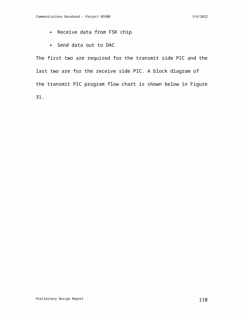
Communications Baseband – Project 05500 5/8/2023
FM Receiver SchematicJ. Riesbeck1/27/2005
Preliminary Design Report 110
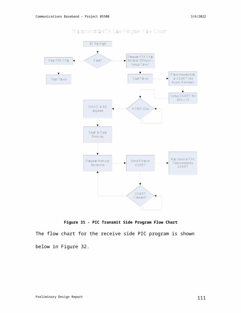
Communications Baseband – Project 05500 5/8/2023
Parts List – FM ReceiverJ. Riesbeck2/1/2005
Preliminary Design Report 111
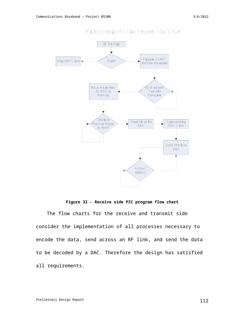
Communications Baseband – Project 05500 5/8/2023
Interconnection Control Document - FM Receiver BoardJ. Riesbeck1/30/2005
Scope: This document outlines the Input/Output connectors on the FM Receiver Board. Pin-outs will be covered. This document will contain all the necessary information to communicate and control the FM Receiver Board.
IO Connectors:Connector J1Pin Description Signal type Cable Type Max Voltage/Current1 RF In RF Coaxial -Type SMA Female
Connector J2Pin Description Signal type Cable Type Max Voltage/Current1 Reserved2 Audio Out Analog Single conductor 100mV/Type 1x2 .1” on center Header
Connector J3Pin Description Signal type Cable Type Max Voltage/Current1 Ground Gnd Single conductor 0/30mA2 Supply Voltage Pwr Single conductor 15V/30mAType 1x2 .1” on center Header
Preliminary Design Report 112
Communications Baseband – Project 05500 5/8/2023
FM Receiver SchematicJ. Riesbeck1/25/2005
Preliminary Design Report 113

Communications Baseband – Project 05500 5/8/2023
Parts List – FSK TransceiverJ. Riesbeck2/1/2005
Preliminary Design Report 114
Communications Baseband – Project 05500 5/8/2023
Interconnection Control Document - GFSK BoardJ. Riesbeck1/29/2005
Scope: This document outlines the Input/Output connectors on the GFSK board. Pin-outs will be covered as well as data timing and control word architecture. This document will contain all the necessary information to communicate and control the GFSK board.
IO Connectors:Connector J1Pin Description Signal type Cable Type Max Voltage/Current1 RF Out/In RF Coaxial 3dBmType SMA Female
Connector J2Pin Description Signal type Cable Type Max Voltage/Current1 Data RX and TX Digital Single conductor 3.6V/2 Clock for TX/RX Digital Single conductor 3.6V/3 Data Ready (RX) Digital Single conductor 3.6V/4 Chip Select Digital Single conductor 3.6V/5 RX Data (Ch2) Digital Single conductor 3.6V/6 Clock (Ch2) Digital Single conductor 3.6V/7 Data Ready (Ch2) Digital Single conductor 3.6V/8 Chip Enable Digital Single conductor 3.6V/9 Power Up Digital Single conductor 3.6V/10 ReservedType 2x5 .1” on center Header
Connector J3Pin Description Signal type Cable Type Max Voltage/Current1 Ground Gnd Single conductor 0/15mA2 Supply Voltage Pwr Single conductor 15V/15mAType 1x2 .1” on center Header
See GFSK Board Protocol Guidelines.
Preliminary Design Report 115
Communications Baseband – Project 05500 5/8/2023
GFSK Board Protocol GuidelinesJ. Riesbeck9/10/2005
Scope: This document describes the process of sending data to the FSK board for the purpose of configuration, transmitting, and reception. Data formatting and timing will be discussed.
Figure 1 – Function Control Pins
Pin DescriptionPWR_UP Power UpCE Chip EnableCS Chip SelectCLK1 Data Clock (Channel 1)DATA1 Data (Channel 1)DR1 Data Ready (Channel 1)*CLK2 Data Clock (Channel 2)*DATA2 Data (Channel 2)*DR2 Data Ready (Channel 2)
Table 1 – Pin Summary*Not used in this application, See NRF2401 datasheet for incorporation
Power Up:To turn on the transceiver set the PWR_UP high (3.3V).
Power Down: Ser PWR_UP low (0V). As long as power is supplied to the board, the control word will be maintained in power down mode. Current consumption is reduced to 1uA in this mode.
Preliminary Design Report 116
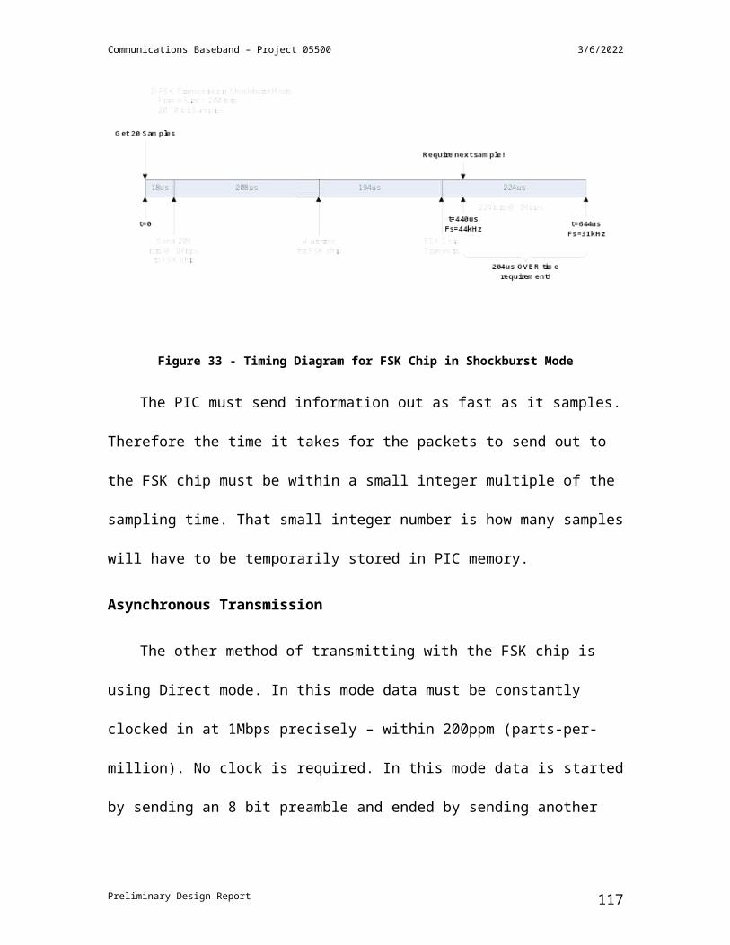
Communications Baseband – Project 05500 5/8/2023
Main Operation Modes:Mode Chip Enable (CE) Chip Select (CS)Configuration 0 1Stand By 0 0Active (RX/TX) 1 0
Table 2 – nRF2401 Chip Modes
Configuration:Configuration settings are necessary for general chip operation and protocol setting. The protocol can be configured in one of two modes; SockBurstTM or Direct.
In direct mode the device operates like a typical RF transceiver where encoding and synchronization are handled by a connected microcontroller. This configuration will not be used for this application. See NRF2401 datasheet for configuration in this mode.
In SockBurstTM the receiver will handle all RF protocol and synchronization automatically. Both receiver and transmitter should be configured identically with the same address. Table 3 shows the proposed settings for this project and their proposed bit values.
Bits Value Binary DescriptionD119:D118 100 01100100 Payload Width (Channel 2)D111:D104 100 01100100 Payload Width (Channel 1)D103:D63 85 ...01010101 Address (Channel 2)D62:D24 85 …01010101 Address (Channel 1)D23:D18 8 001000 Address WidthD17 8-bits 0 CRC Code LengthD16 Enable 1 CRC EnableD15 One 0 Number of ChannelsD14 ShockBurst 1 Communication ModeD13 1Mbps 1 Data Rate (1M/250k)D12:D10 16MHz 011 Crystal FrequencyD9:D8 0dB 11 RF PowerD7:D1 2408MHz 0001000 RF ChannelD0 TX/RX 0/1 Transmit or Receiver Select
Table 3 – Control Word Values
Resulting Configuration Word in Hex:646400000000550000000055216F11
X=0 for Transmit, 1 for Receive
Procedure for sending Configuration Word:1. Set “CS” pin high and wait at least 5us. 2. Start Clocking data in at less than 1Mbps (data on “Data1” and clock on
“Clock1”)3. Data is read on the raising edge of the clock. 4. After the 120bit configuration word, set the “CS” pin low again.
Preliminary Design Report 117
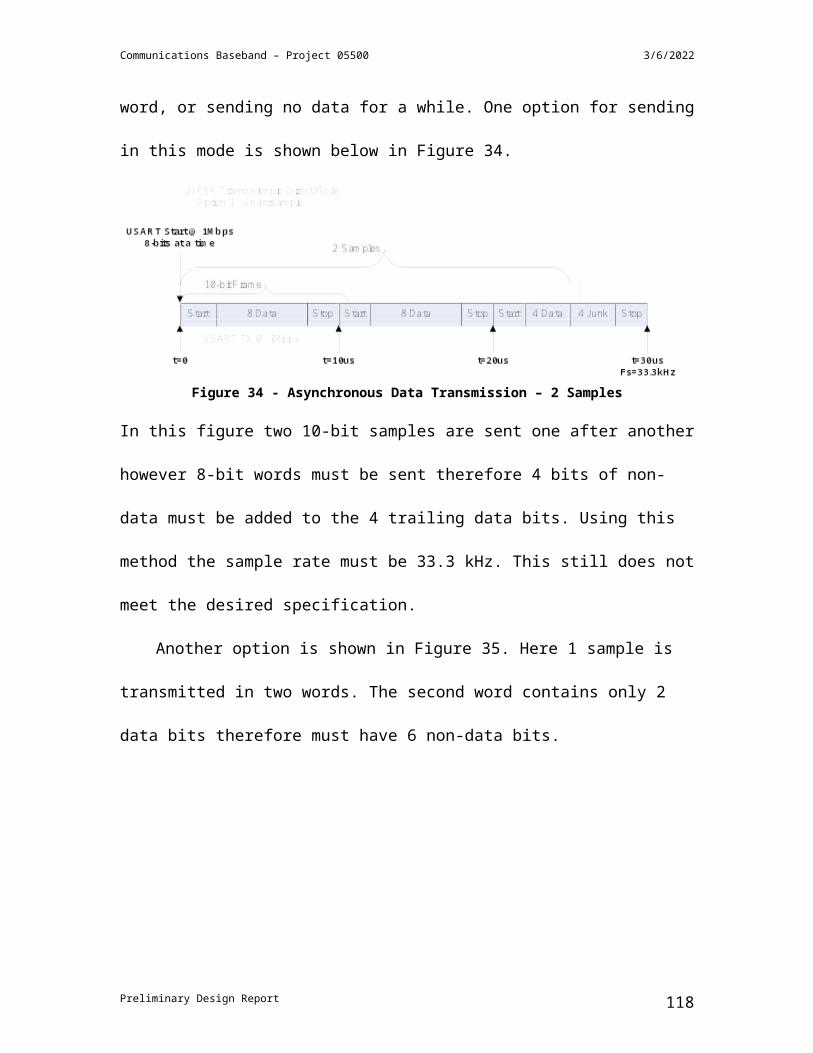
Communications Baseband – Project 05500 5/8/2023
ShockBurst:The ShockBurst feature on this board will automatically CRC code, transmitter,
receive, decode, and store the data packet.
Figure 2 – Packet Path
The transmitting micro controller must supply the board with a data packet (including address configured above).
Procedure for sending data packet:1. Set “CE” pin high and wait at least 5us. 2. Start clocking the data packet data at less than 1Mbps (data on “Data1” pin and
clock on “Clock1” pin)3. Data is read on the raising edge of the clock. 4. After the entire data word is sent, set the “CE” pin low again.
Procedure for receiving data packet:1. Set “CE” pin high. This instructs the receiver to start listening for data.2. When a packet is received by the receiver, the data ready (DR) pin will go high.3. Start clocking out the data packet data at less than 1Mbps (data on “Data1” pin
and clock on “Clock1” pin)4. Data is read on the raising edge of the clock. 5. After the entire data word is sent, set the “CE” pin low again.
Preliminary Design Report 118
Communications Baseband – Project 05500 5/8/2023
GFSK Control WordJ. Riesbeck1/29/2005
Preliminary Design Report 119

Communications Baseband – Project 05500 5/8/2023
Further Look into ISM Band RegulationsJ. Riesbeck1/15/2005
Scope:This document covers the power level limitations for an ISM band implementation.
As per FCC regulations document (refferance1B):
“ TITLE 47--TELECOMMUNICATION CHAPTER I--FEDERAL COMMUNICATIONS COMMISSION PART 15--RADIO FREQUENCY DEVICES--Table of Contents Subpart C--Intentional Radiators Sec. 15.247 Operation within the bands 902-928 MHz, 2400-2483.5 MHz, and 5725-5850 MHz.
(a) Operation under the provisions of this section is limited to frequency hopping and digitally modulated intentional radiators that comply with the following provisions:
… (b) The maximum peak output power of the intentional radiator shall not exceed the following:… (3) For systems using digital modulation in the 902-928 MHz, 2400-2483.5 MHz, and 5725-5850 MHz bands: 1 Watt. (4) Except as shown in paragraphs (b)(3) (i), (ii) and (iii)
of this section, if transmitting antennas of directional gain greater than 6 dBi are used the peak output power from the intentional radiator shall be reduced below the stated values in paragraphs (b)(1) or (b)(2) of this section, as appropriate, by the amount in dB that the directional gain of the antenna exceeds 6 dBi.”
Conclusion:Transmissions are limited to 1watt or +30dBm
Antenna Gain:Per section 15.247.b.4 antenna gain can be as much as 6dB. After which, the transmit power must be reduced by 1dB for every 1dB increase in antenna gain.
Preliminary Design Report 120
Communications Baseband – Project 05500 5/8/2023
Choosing CapacitorsWhat does NP0, C0G, and X7R mean and why does it matter?J. Riesbeck2/8/05
Scope: This document explores the dielectric characteristics available for capacitors and why they should be considered
The capacitance of all capacitors will change if their operating temperature deviates from room temperature. At first this may not appear to be a concern for implementations that are used strictly in temperature controlled areas. However, the fact remains that all electrical circuits consume power and there for produce heat. Therefore, the value of a capacitor may change as the circuit board/chassis warms to operating temperature. Also, all capacitors have associated with them an equivalent series resistance (ESR). This resistance dictates how much power the capacitor itself will consume, which in some cases is enough to result in a measurable heat and therefore change in capacitance.
Another major consideration is a capacitors tendency to change effective capacitance over a range of frequencies. This phenomenon is often much more drastic than the change due to temperature. Typically, the more a component changes with temperature, the more it with change with frequency.
Different types if dielectrics will be represented by a three character long alphanumeric series. Some of the more common coefficients are listed below.
X5RX7RY5VZ5UCOG (same as NP0)
These codes will tell you how much the capacitance will change over temperature. Table (1) contains the information necessary to decipher the temperature coefficients.
Preliminary Design Report 121
Communications Baseband – Project 05500 5/8/2023
First LetterLow Temperature Limit
Center DigitHigh Temperature Limit
Last LetterMax Capacitance Change
C = -55°C 0 = +125°C F = +/- 7.5%X = -55°C 5 = +84°C G = +/- 30PPM/°CY = -30°C 6 = +105°C P = +/- 10%Z = +10°C 7 = +125°C R = +/- 15%
8 = +150°C S = +/- 22%T = +22% / -33%
U = +22% / -56%V = +22% / -82%
Table 1 – Temperature Coefficient Decoding
C0G capacitors obviously have the best performance with a maximum capacitance change of only 0.03% over their temperature range.
Figure 1 – C0G (NP0) Capacitance Performance
Figure 2 –X7R Capacitance Performance
Preliminary Design Report 122
Communications Baseband – Project 05500 5/8/2023
Figures 1 and 2 shows the differences between a NP0 and X7R capacitor performance (from the datasheet for AVX brand size 0805 capacitors).
Conclusion:It is quite obvious from figures 1 and 2 that the change in capacitance from some dielectrics can be drastic. Special attention is paid to the to frequency graph in figure 2. This graph indicates that a X7R capacitor would have a completely different effective capacitance if used in out 2.4GHz system. Furthermore, we do not have the recourses to perform a Monte Carlo analysis on our system because model information does not exist for the components we are using. Therefore it is hard to tell which components in our design need to be of a quality dielectric and which do not.
The best course of action would be to purchase NP0 type for all caps which are connected
to RF paths. NP0 caps are roughly %25 more expensive then their cheaper counterparts
meaning this decision has a minute affect on the cost of the
Preliminary Design Report 123


![[PPT]PowerPoint Presentationedge.rit.edu/edge/OldEDGE/public/Archives/P06201/PDR.ppt · Web viewTitle PowerPoint Presentation Last modified by brl4482 Created Date 1/1/1601 12:00:00](https://img.pdfslide.us/doc/110x75/5ab71b827f8b9ab7638e764e/pptpowerpoint-viewtitle-powerpoint-presentation-last-modified-by-brl4482-created.jpg)