Embed Size (px)
Citation preview

10–1
Table of Contents
Kilovac Solid State Relays
Kilovac Solid State Relays
10
Catalog 5-1773450-5 Dimensions are shown for Dimensions are in millimeters USA: +1 800 522 6752 For additional support numbersRevised 3-13 reference purposes only. unless otherwise specified. Asia Pacific: +86 0 400 820 6015 please visit www.te.com
Specifications subject UK: +44 800 267 666www.te.com to change.
DS11 Series DC Relays, 2 Amp Output Rating, Qualified to DSCC Drawing 88062 . . . . . . . . . . . . . . . . . . . . . . . . . . . . . . . . . . .10-2 – 10-5
DS13 Series DC Relays, 2 Amp Output Rating, Qualified to DSCC Drawing 90091 . . . . . . . . . . . . . . . . . . . . . . . . . . . . . . . . . . .10-6 – 10-9
MS14 Series Solid State Relay . . . . . . . . . . . . . . . . . . . . . . . . . . . . . . . . . . . . . .10-10, 10-11
JTS5, 6, & 7 Series, DC & Bi-Directional Output, Up to 250mA & 250V Output Rating, TO-5 Package, Qualified to MIL-PRF-28750/5, /6, & /7 . . . . . . . . . . . . . . . . . . . . . . .10-12
MS18 Series, DC & Bi-Directional Output, Up to 2A & 350V Output Rating, Qualified to DSCC Drawing 89116 . . . . . . . . . . . . . . . . . . . . . . . . . . . . . . . . . .10-13, 10-14
JDS9 Series, AC Relays, 2A/250Vrms Rating, Qualified to MIL-PRF-28750/9 . . .10-15, 10-16
PS12 Series, AC Relays, 10A/250Vrms Rating, Qualified to DSCC Drawing 86031 . . . . . . . . . . . . . . . . . . . . . . . . . . . . . . . . . .10-17, 10-18
JPS10 Series, AC Relays, 25A/250Vrms Rating, Qualified to MIL-PRF-28750/10 . . . . . . . . . . . . . . . . . . . . . . . . . . . . . . . . . . . .10-19, 10-20
10–2
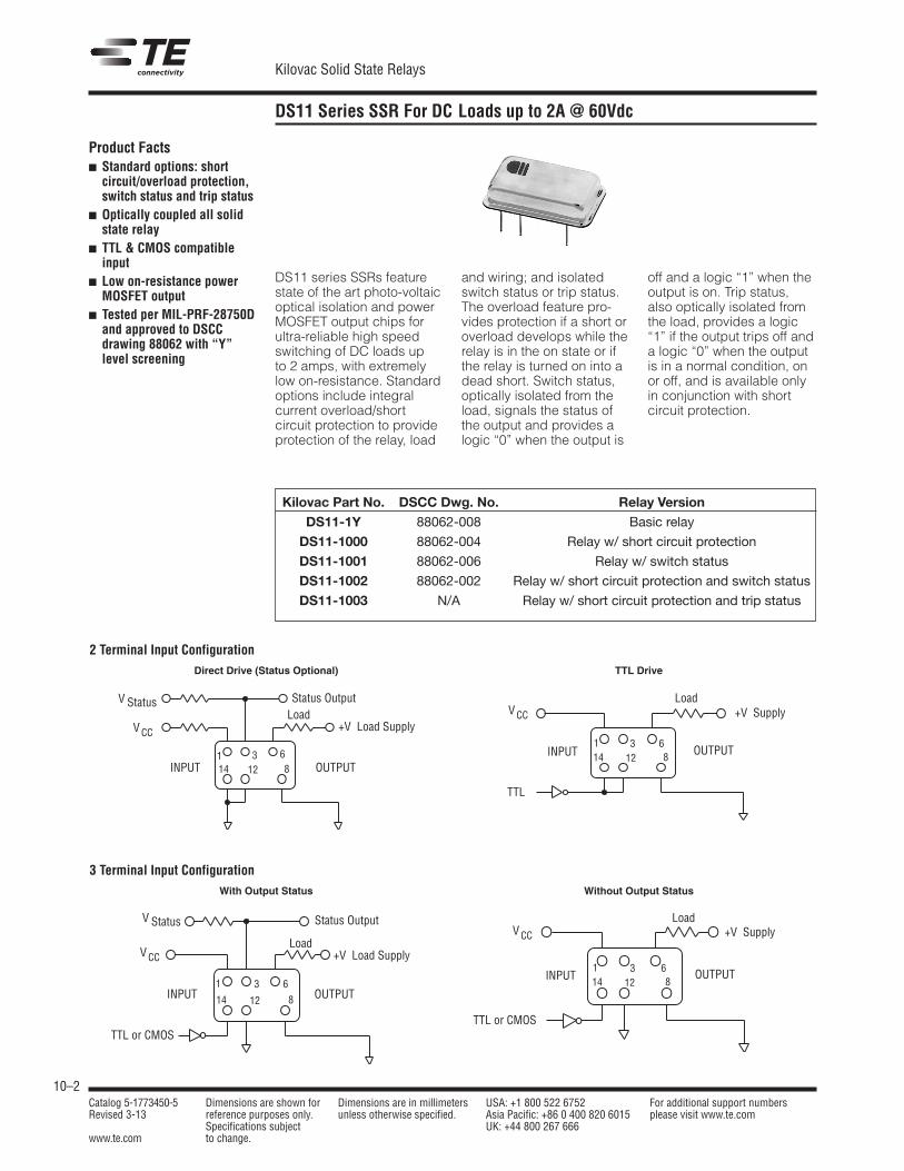
DS11 Series SSR For DC Loads up to 2A @ 60Vdc
Kilovac Solid State Relays
Catalog 5-1773450-5 Dimensions are shown for Dimensions are in millimeters USA: +1 800 522 6752 For additional support numbersRevised 3-13 reference purposes only. unless otherwise specified. Asia Pacific: +86 0 400 820 6015 please visit www.te.com
Specifications subject UK: +44 800 267 666www.te.com to change.
Product Factsn Standard options: shortcircuit/overload protection,switch status and trip status
n Optically coupled all solidstate relay
n TTL & CMOS compatibleinput
n Low on-resistance powerMOSFET output
n Tested per MIL-PRF-28750Dand approved to DSCCdrawing 88062 with “Y”level screening
DS11 series SSRs featurestate of the art photo-voltaicoptical isolation and powerMOSFET output chips forultra-reliable high speedswitching of DC loads up to 2 amps, with extremelylow on-resistance. Standardoptions include integral current overload/short circuit protection to provideprotection of the relay, load
and wiring; and isolatedswitch status or trip status.The overload feature pro-vides protection if a short oroverload develops while therelay is in the on state or ifthe relay is turned on into adead short. Switch status,optically isolated from theload, signals the status ofthe output and provides alogic “0” when the output is
off and a logic “1” when theoutput is on. Trip status,also optically isolated fromthe load, provides a logic“1” if the output trips off anda logic “0” when the outputis in a normal condition, onor off, and is available onlyin conjunction with short circuit protection.
Kilovac Part No. DSCC Dwg. No. Relay Version
DS11-1Y 88062-008 Basic relay
DS11-1000 88062-004 Relay w/ short circuit protection
DS11-1001 88062-006 Relay w/ switch status
DS11-1002 88062-002 Relay w/ short circuit protection and switch status
DS11-1003 N/A Relay w/ short circuit protection and trip status
2 Terminal Input Configuration
3 Terminal Input Configuration
Status Output
+V Load SupplyLoad
V Status
V CC
INPUT OUTPUT1 3 6
81214
+V SupplyLoad
V CC
INPUT OUTPUT
TTL
1 3 681214
Status Output
+V Load SupplyLoad
V Status
V CC
INPUT OUTPUT1 3 6
81214
TTL or CMOS
+V SupplyLoad
V CC
INPUT OUTPUT
TTL or CMOS
1 3 681214
TTL DriveDirect Drive (Status Optional)
Without Output StatusWith Output Status

10–3
DS11 Series SSR For DC Loads up to 2A @ 60Vdc (Continued)
Kilovac Solid State Relays
Kilovac Solid State Relays
10
Catalog 5-1773450-5 Dimensions are shown for Dimensions are in millimeters USA: +1 800 522 6752 For additional support numbersRevised 3-13 reference purposes only. unless otherwise specified. Asia Pacific: +86 0 400 820 6015 please visit www.te.com
Specifications subject UK: +44 800 267 666www.te.com to change.
Electrical Specifications (-55°C to +105°C unless otherwise specified)
Input (2 terminal configuration)
Input supply voltage range (Vcc) 3.8 - 32 Vdc (Notes 1 & 2, Figures 1 & 2)
Input current (max.) @ 5Vdc 15mAdc (Notes 1 & 2, Figures 1 & 2)
Must turn-on voltage 3.8Vdc
Must turn-off voltage 1.5Vdc
Reverse voltage protection -32Vdc
Input (3 terminal configuration)
Control voltage range 0 - 18 Vd
Control current (max.) 250µAdc @ 5V, 1mA @ 18V
Input supply voltage range (Vcc) 3.8 - 32 Vdc (Notes 1 & 2, Figures 1 & 2)
Input current (max.) @ 5Vdc 15mADC (Notes 1 & 2, Figures 1 & 2)
Must turn-on voltage 0.3Vdc
Must turn-off voltage 3.2Vdc
I/O
Dielectric strength (min.) 1,000V rms
Insulation resistance (min.) @ 500Vdc 109 ohms
Capacitance (max.) 10pF
Output
Continuous load current (max.) @ 25°C 2.1Adc (Figure 7)
Continuous load voltage (max.) 60Vdc
Transient blocking voltage (max.) 80Vdc (Note 5)
On resistance (max.) @ Tj = 25°C, IL = 100mA 0.15 ohm (Note 6, Figure 6)
Output voltage drop (max.) 0.5Vdc
Leakage current (max.) @ V = 60Vdc 100µAdc
Leakage current (max.) @ V = 60Vdc, with switch status 2mAdc
Turn-on time (max.) 3 ms (Figure 3)
Turn-off time (max.) 1 ms (Figure 3)
dv/dt (min.) 100V / µs
Electrical system spike 600Vdc (Note 5)
Output chip junction temperature (max.) 125°C
Thermal resistance (max.), junction to ambient 90°C/W
Thermal resistance (max.), junction to case 25°C/W
Status
Status supply voltage range 1 - 18Vdc
Status current (max.) @ Vstatus ≤ 0.4Vdc 600µADC (Figure 5, Note 8)
Status leakage current (max.) @ 16Vdc 10µAdc
Status turn-on time (max.) 3.5 ms (Figure 4)
Status turn-off time (max.) 8 ms (Figure 4)
Short Circuit Protection
Current surge without tripping (max.), 100ms pulse 4.25Adc
Overload trip current (max.), 0.5 ms pulse, V = 60Vdc 10Adc
Trip time (typical), turning on into short 400µs
Trip time (typical), shorting while relay is on 280µs
Environmental CharacteristicsAmbient Temperature Range— Operating — -55°C to +105°CStorage — -55°C to +105°CVibration Resistance— 100 G’s, 10-3,000 HzShock Resistance— 50 G’s, 11 ms pulseConstant Acceleration Resistance(Y1 axis)— 5,000 G’s
Mechanical CharacteristicsWeight (approx.)— .176 oz. (5 grams)Materials— Header — KOVAR Cover — NickelPins — KOVAR, gold plated
KOVAR is a trademark of CarpenterTechnology Corporation.

10–4
DS11 Series SSR For DC Loads up to 2A @ 60Vdc (Continued)
Kilovac Solid State Relays
Catalog 5-1773450-5 Dimensions are shown for Dimensions are in millimeters USA: +1 800 522 6752 For additional support numbersRevised 3-13 reference purposes only. unless otherwise specified. Asia Pacific: +86 0 400 820 6015 please visit www.te.com
Specifications subject UK: +44 800 267 666www.te.com to change.
Figure 1 - Maximum Input Current vs. Input Voltage Figure 2 - Series Resistance vs. Vcc Supply Voltage (Note 1)
Input Voltage, Vcc (Vdc)
Inpu
t Cur
rent
(mA)
18
15
12
9
6
3
00 5 10 15 20 25 30 40 50 60
Vcc (Volts)
R S
erie
s (o
hms)
300
600
900
1200
1500
1800
00 6 10 15 20 25 30 35
Figure 5 - Status Resistor vs. Status Supply Voltage Figure 6 - On-Resistance vs. Temperature (Note 6)
Status Supply Voltage (Volts)
Stat
us R
esis
tor (
ohm
s)
35000
30000
25000
20000
15000
10000
5000
00 5 10 15 20
Junction Temperature (°C)
Nor
mal
ized
On
Res
ista
nce
Fact
or(N
R)
0.025 50 75 100 125
0.20.4
0.60.8
1.21.0
1.41.61.82.0
Figure 3 - Turn-on and Turn-off Timing Figure 4 - Output Status Timing
Pin 14(Input)
Pin 6-8
High
Low
Off
OnT TOn Off
90%10%
T
T
V
V
Control
S
50%
90%
10%
StatusTurn-OffTime
StatusTurn-OnTime
OFF
ON

10–5
DS11 Series SSR For DC Loads up to 2A @ 60Vdc (Continued)
Kilovac Solid State Relays
Kilovac Solid State Relays
10
Catalog 5-1773450-5 Dimensions are shown for Dimensions are in millimeters USA: +1 800 522 6752 For additional support numbersRevised 3-13 reference purposes only. unless otherwise specified. Asia Pacific: +86 0 400 820 6015 please visit www.te.com
Specifications subject UK: +44 800 267 666www.te.com to change.
Notes1.2 terminal input configuration is compatible with CMOS or open collector TTL (with pull-up resistor). For Vcc levels above 6Vdc, a series limiting resistor isrequired. See Fig. 2 for resistor value. Use standard resistor value equal to or less than value from the curve.
2.Input transitions to be ≤ 1ms duration, and input direct drive should be “bounceless contact” type.3. Vcc = 5Vdc for all tests unless otherwise specified.
4.All DS11 Series relays may drive loads connected to either positive or negative referenced power supply lines. Reversing polarity of output may cause permanentdamage. Inductive loads must be diode suppressed.
5.Transient blocking voltage and electrical system spike tests are performed per MIL-STD-704 (28VDC systems).
6.To determine the maximum on-resistance at any given junction temperature, multiply on-resistance at 25°C (0.15 ohm) by normalized on-resistance factor fromcurve (Fig. 6).
7.Overload testing per MIL-R-28750 is constrained to the limits imposed by the short circuit protection requirements of this specification and DSCC drawing 88062.Load circuit series inductance for “load shorted” mode of operation to be limited to 50mH max. Maximum repetition rate into a shorted load should not exceed 10 Hz.
8.Proper operation of the status feedback requires a status pull-up resistor. See Fig. 5 for status resistor value.
Figure 7 - Temperature Derating Curve
Ambient Temperature (°C)
Out
put C
urre
nt (a
mps
)
00.20.40.60.81.01.21.41.61.82.0
-50 -40 -20 0 20 40 60 80 100 120
Figure 9 - Outline Dimensions
.140(3.55)
.500(12.70).600
(15.24)
.300(7.62)
.110(2.79)
.530 MAX(13.46)
.850 REF.(21.59)
.273 ±.020(6.93 ± .50)
.020 MAX.(.50)
.190 MAX.(4.82)
.200(5.08)
.890 MAX.(22.60)
.490 REF.(12.44)
.017 +.002, –.001 DIA.(.43 + .05, –.02)
6 PLS.
DATE CODEHERE
TOP MARKINGORIENT AS
SHOWN
TOLERANCE:± 0.010 (0.25mm) FOR 2 PLACE DECIMALS,± 0.005 (0.13mm) FOR 3 PLACE DECIMALS.UNLESS OTHERWISE SPECIFIED
Figure 8 - Maximum Surge Current Without Tripping
Time (seconds)
Surg
e Cu
rren
t (am
ps)
1.0
2.0
3.0
4.0
5.0
6.0
7.0
0.01 0.1 1 10
+85°C
+25°C
-55°C

10–6
DS13 SSR for loads up to 2A @ 60Vdc
Kilovac Solid State Relays
Catalog 5-1773450-5 Dimensions are shown for Dimensions are in millimeters USA: +1 800 522 6752 For additional support numbersRevised 3-13 reference purposes only. unless otherwise specified. Asia Pacific: +86 0 400 820 6015 please visit www.te.com
Specifications subject UK: +44 800 267 666www.te.com to change.
Product Factsn Standard options: shortcircuit/overload protectionand control status.
n Optically coupled all solidstate relay.
n TTL & CMOS compatibleinput.
n Low on-resistance powerMOSFET output.
n Tested per MIL-PRF-28750Dand approved to DSCCdrawing 90091.
n All versions available withTyco Electronics “W” levelscreening for Kilovacrelays.
DS13 series SSRs employstate of the art photovoltaicoptical isolation and powerMOSFET output chips forultra-reliable high speedswitching of DC loads up to 2 amps, with low on-resistance. Standardoptions include integral current overload/short
circuit protection and a separate input control status line. The overloadfeature provides protectionof the relay, load and loadcircuit wiring in the event ofa sustained current over-load or short circuit whilethe relay is on or when it isturned on into a short. The
control status provides abuilt-in test function whichprovides a logic “0” whenthe input circuit is energizedand functional. The relay ispackaged into a customhermetically sealed low-profile 8-pin ceramic DIPpackage, with through holeor surface mount pins.
Kilovac Part No. DSCC Dwg. No. Relay Version
DS13-1Y 90091-008 Basic relay
DS13-1000 90091-004 Relay w/ short circuit protection
DS13-1001 90091-006 Relay w/ control status
DS13-1002 90091-002 Relay w/ short circuit protection and control status
Notes: Add suffix “S” to part number for surface mount versions.Add suffix “T” to part number for tinned leads.Add suffix “W” to part number for lower screening level.
2 Terminal Input Configuration
Load
Load
R SeriesS1
Vcc
Control
1
2
8
4
5
Return
(-) Output
(+) OutputV Load
LoadReturn
Load
Load
R SeriesVcc
Control
1
2
8
4
5
Return
(-) Output
(+) OutputV Load
LoadReturn
O C TTL
Load
Load
VccVso
Control
1
2
8
4
5
Return
(-) Output
(+) OutputV Load
LoadReturn
7
V
R
Status
Status
VControl
StatusOutput Load
Load
Vcc
Control
1
2
8
4
5
Return
(-) Output
(+) OutputV Load
LoadReturn
VControl
TTL DriveDirect Drive
3 Terminal Input ConfigurationWithout StatusWith Status
10–7
DS13 SSR for loads up to 2A @ 60Vdc (Continued)
Kilovac Solid State Relays
Kilovac Solid State Relays
10
Catalog 5-1773450-5 Dimensions are shown for Dimensions are in millimeters USA: +1 800 522 6752 For additional support numbersRevised 3-13 reference purposes only. unless otherwise specified. Asia Pacific: +86 0 400 820 6015 please visit www.te.com
Specifications subject UK: +44 800 267 666www.te.com to change.
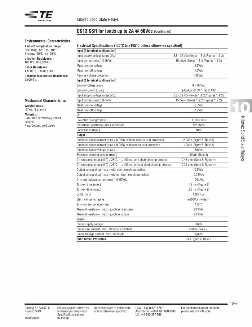
Electrical Specifications (-55°C to +105°C unless otherwise specified)Input (2 terminal configuration)
Input supply voltage range (Vcc) 3.8 - 32 Vdc (Notes 1 & 2, Figures 1 & 2)
Input current (max.) @ 5Vdc 15mAdc (Notes 1 & 2, Figures 1 & 2)
Must turn-on voltage 3.8Vdc
Must turn-off voltage 1.5Vdc
Reverse voltage protection -32Vdc
Input (3 terminal configuration)
Control voltage range 0 - 18 Vdc
Control current (max.) 240µAdc @ 5V, 1mA @ 18V
Input supply voltage range (Vcc) 3.8 - 32 Vdc (Notes 1 & 2, Figures 1 & 2)
Input current (max.) @ 5Vdc 15mAdc (Notes 1 & 2, Figures 1 & 2)
Must turn-on voltage 0.3Vdc
Must turn-off voltage 3.2Vdc
I/O
Dielectric Strength (min.) 1,000V rms
Insulation Resistance (min.) @ 500Vdc 109 ohms
Capacitance (max.) 10pF
Output
Continuous load current (max.) @ 25°C, without short circuit protection 2.0Adc (Figure 5, Note 3)
Continuous load current (max.) @ 25°C, with short circuit protection 1.0Adc (Figure 5, Note 3)
Continuous load voltage (max.) 60Vdc
Transient blocking voltage (max.) 80Vdc (Note 4)
On resistance (max.) @ Tj = 25°C, IL = 100ma, with short circuit protection 0.45 ohm (Note 5, Figure 4)
On resistance (max.) @ Tj = 25°C, IL = 100ma, without short circuit protection 0.22 ohm (Note 5, Figure 4)
Output voltage drop (max.), with short circuit protection 0.6Vdc
Output voltage drop (max.), without short circuit protection 0.75Vdc
Off-state leakage current (max.) @ 60Vdc 100µAdc
Turn-on time (max.) 1.5 ms (Figure 3)
Turn-off time (max.) .25 ms (Figure 3)
dv/dt (min.) 100V / µs
Electrical system spike ±600Vdc (Note 4)
Junction temperature (max.) 150°C
Thermal resistance (max.), junction to ambient 80°C/W
Thermal resistance (max.), junction to case 20°C/W
Status
Status supply voltage 30Vdc
Status sink current (max.) @ Vstatus≤ 0.3Vdc 2mAdc (Note 7)
Status leakage current (max.) @ 15Vdc 4µAdc
Short Circuit Protection See Figure 6, Note 7
Environmental CharacteristicsAmbient Temperature Range:Operating: -55°C to +105°C.Storage: -55°C to +125°C.
Vibration Resistance:100 G’s, 10-3,000 Hz.
Shock Resistance:1,500 G’s, 0.5 ms pulse.
Constant Acceleration Resistance:5,000 G’s.
Mechanical CharacteristicsWeight (max.):.07 oz. (2 grams)
Materials:Case: DIP, hermetically sealed,ceramicPins: Copper, gold plated

10–8
DS13 SSR for loads up to 2A @ 60Vdc (Continued)
Kilovac Solid State Relays
Catalog 5-1773450-5 Dimensions are shown for Dimensions are in millimeters USA: +1 800 522 6752 For additional support numbersRevised 3-13 reference purposes only. unless otherwise specified. Asia Pacific: +86 0 400 820 6015 please visit www.te.com
Specifications subject UK: +44 800 267 666www.te.com to change.
Figure 1 - Maximum Input Current vs. Input Voltage Figure 2 - Series Resistance vs. Vcc Supply Voltage (Note 1)
Input Voltage, Vcc (Vdc)
Inpu
t Cur
rent
(mA)
18
15
12
9
6
3
00 5 10 15 20 25 30 40 50 60
Vcc (Volts)
R S
erie
s (o
hms)
500
1000
1500
2000
00 5 10 15 20 25 30 35
Figure 5 - Temperature Derating Curve Figure 6 - Typical Current Trip Levels
0.0
0.5
1.0
2.0
1.5
-55 15 25 35 45 55 65 75 85 95 105 115 125
Load
Cur
rent
(am
ps)
Ambient Temperature (°C)
DS13-1YDS13-1001
DS13-1000DS13-1002
5
4
3
2
1
00.10.01 1 10 100 1000
Surg
e Cu
rren
t (am
ps)
Time (seconds)
-55°C+25°C
+105°C
Figure 3 - Output Turn-on and Turn-off Timing Figure 4 - On-Resistance vs. Temperature (Note 6)
Pin 4-5
High
Low
Off
On
T TOn Off
90%10%
V
V
Control
Output
Pin 2
Junction Temperature (°C)
Nor
mal
ized
On
Res
ista
nce
Fact
or (N
F)
25 50 75 100 1250.20.40.60.8
1.21.0
1.41.61.82.0

10–9
DS13 SSR for loads up to 2A @ 60Vdc (Continued)
Kilovac Solid State Relays
Kilovac Solid State Relays
10
Catalog 5-1773450-5 Dimensions are shown for Dimensions are in millimeters USA: +1 800 522 6752 For additional support numbersRevised 3-13 reference purposes only. unless otherwise specified. Asia Pacific: +86 0 400 820 6015 please visit www.te.com
Specifications subject UK: +44 800 267 666www.te.com to change.
Notes1.2 terminal input configuration is compatible with CMOS or open collector TTL (with pull-up resistor). For Vcc levels above 6Vdc, a series limiting resistor isrequired. See Fig. 2 for resistor value. Use standard resistor value equal to or less than value form the curve.
2.Vcc = 5Vdc for all tests unless otherwise specified.
3.All DS13 Series relays may drive loads connected to either positive or negative referenced power supply lines. Reversing polarity of output may cause permanentdamage. Inductive loads must be diode suppressed.
4.Transient blocking voltage & electrical system spike tests are performed per MIL-STD-704 (28Vdc systems).
5.To determine the maximum on-resistance at any given junction temperature, multiply on-resistance at 25°C by normalized on-resistance factor from curve (Fig. 4).
6.Overload testing per MIL-R-28750 is constrained to the limits imposed by the short circuit protection requirements of this specification and DSCC drawing 90091.Load circuit series inductance for “load shorted” mode of operation to be limited to 50mH max. Maximum repetition rate into a shorted load should not exceed 10 Hz. To calculate maximum on-resistance at any temperature, use the following equation: R(on) = R(on) @ 25°C x NF (without short circuit protection) and R(on) = 0.2 x NF + .21 (with short circuit protection) where NF = normalized on-resistance factor from Fig. 4.
7.Proper operation of the status feedback requires a status pull-up resistor. Select the status resistor such that it limits status output current to 2mA: R status = V status – 0.3V / 2mA.
Figure 7 - Outline Dimensions
421
578
SIDE INDEX MARK FOR PIN 1
TOP INDEX MARK FOR PIN 1
6 PLS
TOP INDEX MARK FOR PIN 1
SIDE INDEX MARK FOR PIN 1
8 7 5
1 2 4
.395 MAX.(10.03)
.560 MAX.(14.22)
.400 ± .015(10.16 ± .38)
.010 ± .002(.25 ± .05)
.560 MAX.(14.22)
.395 MAX.(10.03)
.155 MAX.(3.94)
.155 MAX.(3.94)
.435 MAX.(11.05)
.485 +.010, –.005(12.32 +.25, –.13)
.010 ± .002(.25 ± .05)
6 PLS
.036 +.010, –.005(.91 +.25, –.13)
6 PLS
.018 ± .002(.46 ± .05)
6 PLS
.025(.64)6 PLS
.125(3.18)
.100(2.54) .300
(7.62).125
(3.18)
.100(2.54) .300
(7.62)
.018 ± .002(.46 ± .05)
6 PLS
.016 +.010, –.005(.41 +.25, –.13)
6 PLS
.150 ± .015(3.81 ± .38)
6 PLS
Surface Mount VersionThrough-Hole Mount Version

10–10
MS14 Series Solid State Relay, With DC or Bi-Directional Output to 350mA @ 400V
Kilovac Solid State Relays
Catalog 5-1773450-5 Dimensions are shown for Dimensions are in millimeters USA: +1 800 522 6752 For additional support numbersRevised 3-13 reference purposes only. unless otherwise specified. Asia Pacific: +86 0 400 820 6015 please visit www.te.com
Specifications subject UK: +44 800 267 666www.te.com to change.
Product Factsn 1000V optical isolationprotects control and drivercircuitry from loadtransients.
n Buffered/current limitedinput for direct drive fromCMOS or TTL logic.
n Power MOSFET output chipsfor low voltage drop.
n 90 & 240mA output current.n 85, 100 & 400V outputvoltage.
n Subminiature hermeticallysealed .100 grid package.
n Screened per “Y” level ofMIL-PRF-28750D.
n Direct replacement forTELEDYNE M92F & M93Fseries
Environmental CharacteristicsAmbient Temperature Range:Operating: -55°C to +105°C.Storage: -55°C to +125°C.
Vibration Resistance:30 G’s, 10-3,000 Hz.
Shock Resistance:1,500 G’s, 0.5 ms pulse.
Constant Acceleration Resistance:5,000 G’s.
Mechanical CharacteristicsWeight (max.):.07 oz. (2 grams)
Materials:Case: Nickel, hermetically sealed.Pins: Kovar, gold plated
TTL Configuration
+Vcc
(–)
LOAD
LOAD
5
4
3
7
1CMOS LOADRETURN
VLOAD
CMOS Configuration
+Vcc
LOAD
LOAD
5
4
3
7
1
TTLLOAD
RETURN
VLOAD
MS14 series subminiatureSSRs employ state of the artphoto-voltaic optical isolationproviding 1000Vrms input/out-put isolation and power mosfetoutput chips for ultra-reliable
high speed switching of DC orbidirectional loads up to 350mAand 400Vdc. The input is cur-rent regulated and buffered tominimize power dissipation andpermit driving the relay direct
from CMOS or TTL. The relay ispackaged in a custom hermeti-cally sealed low-profile .100grid package which conservesspace for high density PCboard circuitry.
Kilovac Part No. DSCC Drawing/Pin No. Output Rating
MS14-1Y 85092-001 350mA / 400VMS14-2Y 85092-002 135mA / 400VMS14-3Y 87034-003 ±240mA / 85V
Electrical Specifications (-55°C to +105°C unless otherwise specified)Input (TTL Drive)Input supply voltage range (Vcc) 3.8 - 32 Vdc (Notes 1 & 2, Figures 1 & 2)Input current (max.) @ 5Vdc 16mAdc (Notes 1 & 2, Figures 1 & 2)Must turn-on voltage 3.8VdcMust turn-off voltage 1.5VdcInput (CMOS Drive)Control voltage range 0 - 18 VdcControl current (max.) 250µAdc @ 5V, 1mA @ 18VInput supply voltage range (Vcc) 3.8 - 32 Vdc (Notes 1 & 2, Figures 1 & 2)Input current (max.) @ 5Vdc 16mAdc (Notes 1 & 2, Figures 1 & 2)Must turn-on voltage 0.3VdcMust turn-off voltage 2.8VdcI/ODielectric Strength (min.) 1,000V rmsInsulation Resistance (min.) @ 500Vdc 109 ohms OutputContinuous load current (max.) @ 25°C: MS14-1Y 350mAdcContinuous load current (max.) @ 25°C: MS14-2Y 135mAdcContinuous load current (max.) @ 25°C: MS14-3Y +/– 240mAContinuous load voltage (max.) @ 25°C: MS14-1Y 100VdcContinuous load voltage (max.) @ 25°C: MS14-2Y 400VdcContinuous load voltage (max.) @ 25°C: MS14-3Y +/– 85VOn resistance (max.) @ Tj = 25°C, IL = 100mA: MS14-1Y 4 ohmsOn resistance (max.) @ Tj = 25°C, IL = 100mA: MS14-2Y 25 ohmsOn resistance (max.) @ Tj = 25°C, IL = 100mA: MS14-3Y 8 ohmsOff-state leakage I (max.) @ 80% max. V @ –55 to +25°C 1µAOff-state leakage I (max.) @ 80% max. V @ =25 to +85°C 50µAJunction temperature (max.) 150°CTurn-on time (max.) MS14-1Y & –2Y .7mSTurn-on time (max.) MS14-3Y 2mSTurn-off time (max.) (all versions) 1mS
© 2011 by Tyco Electronics Corporation. All Rights Reserved.TE logo and Tyco Electronics are trademarks. Other products and company names mentioned herein may be trademarks of their respective owners.
Ordering Information

10–11
MS14 Series Solid State Relay, With DC or Bi-Directional Output to 350mA @ 400V (Continued)
Kilovac Solid State Relays
Kilovac Solid State Relays
10
Catalog 5-1773450-5 Dimensions are shown for Dimensions are in millimeters USA: +1 800 522 6752 For additional support numbersRevised 3-13 reference purposes only. unless otherwise specified. Asia Pacific: +86 0 400 820 6015 please visit www.te.com
Specifications subject UK: +44 800 267 666www.te.com to change.
Input Voltage, Vcc (Vdc)
Inpu
t Cur
rent
(mA)
18
15
12
9
6
3
00 5 10 15 20 25 30 40 50 60
Vcc (Volts)
R Se
ries
(ohm
s)500
1000
1500
2000
00 5 10 15 20 25 30 35
Figure 1 - Max. Input Current vs. Input Voltage
Figure 2 - Series Res. vs. Vcc Supply Voltage (Note 1)
Figure 5 - On-Resistance vs. Temperature (Note 6)
Figure 6 - Simplified Circuit
0.00.2
0.6
1.0
1.82.0
1.4
0.4
0.8
1.6
1.2
25 50 75 100 125Norm
alize
d On
Res
. Fac
tor (
NF)
Junction Temperature (°C)
+Vcc
RETURN
5
4
3
CONTROL
+ OUTPUT
– OUTPUT
7
1
Figure 3 -Output Turn-on and Turn-off Timing
Figure 4 -Temperature Derating Curve
High
Low
Off
On
T TOn Off
90%10%
Input
Output
4V8V12V16V20V24V28V32V
0
2010
30
50
90
70
40
80
60
100
25 35 45 55 65 75 85 95 105 115 125
% O
utpu
t Cur
rent
Ambient Temperature (°C)
Input Supply Voltage (Vcc)
Notes1.2 terminal input configuration is compatible with CMOS or open collector TTL (with pull-up resistor).
2.For Vcc levels above 6Vdc, a series limiting resistor is required. See Fig. 2 for resistor value. Use standard resistor value equal to or less than value form the curve.
3.Vcc = 5Vdc for all tests unless otherwise specified.
4.All MS14 Series relays may drive loads connected to either positive or negative referenced power supply lines. Inductive loads must be diode suppressed.
5.If an input series current limiting resistor is used, derating of output current vs. Vcc is not necessary. Curve for 4V applies.
6.On-resistance at any ambient temperature other than 25°C can be computed as follows:R (@ any T) = R (@ +25°C) x e0.006, where T = new temperature – 25°C, e = 2.7182818 .
Figure 7 - Outline Dimensions
.335 [8.51]
SQUARE MAX.
.275 MAX. [6.99] .70 MIN.
[17.8]
.200 TYP. [5.08]
.085 REF. [2.16]
.100 TYP. [2.54]
.370 [9.40]
SQUARE MAX.
.031 ± .002 [.78 ± .05]
.032 [.813]
.085 REF. [2.16]
.100 TYP. [2.54]
7 1
5 34
.080 [2.03] DIA. GLASS BEAD
5 PLACES
CASE TEMPERATURE MEASUREMENT
POINT Unless otherwise specified, tolerances are:±0.010 [0.25] for 2 place decimals±0.005 [0.13] for 3 place decimals
Terminal numbers are for reference only and do not appear on the header.
9-1773439-2–PDF–KRG–9-07
Note:MS14-1Y and -2Y have a single output chip.

10–12
JTS5, 6, & 7 Series, DC & Bi-Directional Output, Up to 250mA & 250V Output Rating, TO-5 Package
Kilovac Solid State Relays
Catalog 5-1773450-5 Dimensions are shown for Dimensions are in millimeters USA: +1 800 522 6752 For additional support numbersRevised 3-13 reference purposes only. unless otherwise specified. Asia Pacific: +86 0 400 820 6015 please visit www.te.com
Specifications subject UK: +44 800 267 666www.te.com to change.
Output Current Vs. Input Control Voltage and Ambient Temperature
Product Factsn Hermetically sealed TO-5package
n Transformer coupledn High speed switchingn JTS5-1Y switches AC or DCn Qualified to M28750/5, 6, & 7
1CONTROLSOURCE
DC SUPPLY
3
7 5
++
1CONTROLSOURCE 3
7 5
LOAD
LOAD
AC OR ±DC SUPPLY
Terminal View
.335 DIA MAX (8.51)
.370 DIA MAX (9.40)
.275 MAX(6.99)
.50 MIN (12.70)
.017 DIA (.43)
.100(2.54)
.200(5.08)
.031 (.79)
.032(REF)(.81)
45°
-60-40-20 20 40 60 80 10012014010
20
30
40 50 60 70 80 90
300
200
100
-60-40-20 20 40 60 80 10012014010
20
30
405060708090
300
200
100
-60-40-20 20 40 60 80 1001201401
2
3 4 5
7
10
20
30 40 50 60
Out
put C
urre
nt (m
A)
–55°
C
–125
°C
–55°
C
–125
°C
–55°
C
–125
°C
0
6 Vdc INPUT
5 Vdc INPUTRATED CURRENT
4 Vdc INPUT
7 Vdc INPUT
0 0
4 Vdc INPUT
Ambient Temperature (°C)
Out
put C
urre
nt (m
A)
Ambient Temperature (°C)
Out
put C
urre
nt (m
A)
Ambient Temperature (°C)
RATED CURRENT5 Vdc INPUT
6 Vdc INPUT7 Vdc INPUT
6 Vdc INPUT
5 Vdc INPUTRATED CURRENT
4 Vdc INPUT
7 Vdc INPUT
Input CharacteristicsInput Voltage Range— 4.0 – 7.0 VdcMaximum Turn-on Voltage— 5.0 VdcMinimum Turn-off Voltage— 1.0 VdcI/O Dielectric— 1000 Vac pk-pk
Output CharacteristicsMax. Output Current (Continuous, 25°C) — 50 mAac or mAdc (JTS5-1Y)250 mAdc (JTS6-1Y)100 mAdc (JTS7-1Y) Max. Output Voltage— 40 Vac or Vdc (JTS5-1Y)40 Vdc (JTS6-1Y)250 Vdc (JTS7-1Y) Max. On-resistance— 5 ohms (JTS5-1Y) Turn-on Time— 10 µsec.Turn-off Time— 15 µsec.
Environmental CharacteristicsShock— 1500 G’s, 0.5 ms. Vibration— 100 G’s, 10 to 2000 HzOperating Ambient Temperature—-55 to +125°C
JTS5/JTS6/JTS7
Notes: 1) Reversing polarity of input (or output except for JTS5-1) may cause permanent damage. 2) Input must be a step function. Rise or fall time, as applicable, not to exceed 100 µsec. 3) Inductive loads must be diode suppressed. 4) For any control voltage, the maximum load current shown on graphs must not be exceeded. Attempting todraw currents in excess of those specified on graphs can cause permanent damage.
JTS5-1Y JTS6-1Y JTS7-1Y

10–13
MS18-1006 High Performance DC and Bi-directionalSolid State Relay For Loads up to 2A @ 80Vdc
Kilovac Solid State Relays
Kilovac Solid State Relays
10
Catalog 5-1773450-5 Dimensions are shown for Dimensions are in millimeters USA: +1 800 522 6752 For additional support numbersRevised 3-13 reference purposes only. unless otherwise specified. Asia Pacific: +86 0 400 820 6015 please visit www.te.com
Specifications subject UK: +44 800 267 666www.te.com to change.
Product Factsn Bi-directional power FEToutput
n Optically coupledn Low on-resistancen Extremely low leakagecurrent
n Subminiature hermeticallysealed package
n Tested per MIL-PRF-28750Dand approved to DSCCdrawing 89116-006
The MS18-1006 is an opti-cally coupled SSR employ-ing power MOSFET outputchips in an inverse seriesconfiguration for switchingDC or bi-directional loads. A common source connec-tion is provided for the user
to configure the outputswitching circuit for DCoperation up to 2A with very low on-resistance. Therelay features fast switchingspeeds, low off-state leakage,virtually zero offset voltageand the capability to with-
stand high inrush currentsup to 350% of rated. Thelow profile subminiaturepackage is hermeticallysealed with pinouts on a0.1” x 0.3” grid pattern.
Kilovac Part No. DSCC Dwg. No. Relay Version
MS18-1006 89116-006 Basic relay
Figure 1 – Wiring Diagrams
V(in) V(load)
RSLOAD
N/C
TOP VIEW
1
2
3
6
5
4CASE�
GROUND
V(in) V(load)
RSLOAD
TOP VIEW
1
2
3
6
5
4CASE
GROUND
Environmental CharacteristicsAmbient Temperature Range— Operating — -55°C to +120°CStorage — -55°C to +125°CVibration Resistance— 100 G’s, 10-2,000 HzShock Resistance— 1,500 G’s, 0.5 ms pulseConstant Acceleration Resistance (Y-1 axis)— 5,000 G’s
Mechanical CharacteristicsWeight (approx.) — .07 oz. (5 grams)Materials— Header — Kovar® Alloy Cover — Grade A NickelPins — Kovar® Alloy, gold plated
Electrical Specifications (-55°C to +120°C unless otherwise specified)Input
Input current (max.) 25mAdc
Input voltage drop (max. @ 25mA)) 1.5 Vdc
Must turn-on current 10mA
Must turn-off current 10µA
Reverse voltage protection -5.0Vdc
I/O
Dielectric strength (60Hz., 1mA leakage) 500V rms
Insulation resistance (min.) @ 500Vdc 109 ohms
Capacitance (max. @ 25Vdc, 1 Mhz) 5pF
Output
Continuous load current, parallel (DC) configuration (max.) 2A (Figure 2)
Continuous load current, series (bi-directional) configuration (max.) 1A (Figure 2)
Continuous operating load voltage (max.) +/– 80V
Transient blocking voltage (5 sec max.) +/– 90V
Overload (100ms, 10% duty cycle, 10 cycles max.) 350% of rated
dv/dt (min.) 100V / µs
On resistance (max.), parallel (DC) configuration 0.4 ohm
On resistance (max.), series (bi-directional) configuration 0.6 ohm
Turn-on time (max, @ +/– 80V) 800µs (Figure 3)
Turn-off time (max, @ +/– 80V) 500µs (Figure 3)
Thermal resistance, junction to ambient 110°C/W
Thermal resistance, junction to case 20°C/W
Parallel ConnectionSeries Connection
KOVAR is a trademark of CarpenterTechnology Corporation.

10–14
MS18-1006 High Performance DC and Bi-directionalSolid State Relay For Loads up to 2A @ 80Vdc (Continued)
Kilovac Solid State Relays
Catalog 5-1773450-5 Dimensions are shown for Dimensions are in millimeters USA: +1 800 522 6752 For additional support numbersRevised 3-13 reference purposes only. unless otherwise specified. Asia Pacific: +86 0 400 820 6015 please visit www.te.com
Specifications subject UK: +44 800 267 666www.te.com to change.
Figure 2 - Temperature Derating Curves
AMBIENT TEMPERATURE (°C)5 15 25 35 45 55 65 75 85 95 105115 125
1.2
1.1
1.0
0.9
0.8
0.7
0.6
0.5
0.4
0.3
0.2
0.1
0
LOAD
CU
RR
ENT
(AM
PS R
MS)
5 15 25 35 45 55 65 75 85 95 105115 125
2.4
2.2
2.0
1.8
1.6
1.4
1.2
1.0
0.8
0.6
0.4
0.2
0
AMBIENT TEMPERATURE (°C)
LOAD
CU
RR
ENT
(AM
PS D
C)
Figure 3 - Turn-on and Turn-off Timing Figure 4 - Functional Block Diagram
PIN 1 REF TO 2
PIN 6 TO 4
T(ON) T(ON)
HIGH
LOW
OFF
ON
90%
10%
FLOATING�POWER SUPPLY
TIMING & SIGNAL
COND.
BIAS
RTN
CASE GND
1
3
2
LINE
RTN
LINE
6
4
5
Figure 5 - Outline Dimensions
± 80
V - 1
.0A
TY
CO
E
LE
CT
RO
NI C
S
MS
18
-10
06
586 14
0.190 MAX. (4.83)0.160
(4.06) MIN.
0.463 MAX. (11.76)0.300 (7.62)
DATE CODE ON�THIS SURFACE
0.020 MAX. (0.508) 6 PLS0.017 +.002, –.001
(0.432 +.051, –.025)
0.084 ±.005 (2.13 ± .127)
0.109 (2.77)
0.200 (5.08)
0.100 (2.54)
0.418 (10.62)
Notes1. An external resistor must be in series with the input at all times.
2. Do not ramp input current. Input transition should be <1.0ms.
3. Input current/series resistor calculation (Approx.): I(input) = VIN – VDROP/RSERIES.
4. Unless otherwise specified parametric testing is accomplished at 25ma input current.
5. To calculate RDS(ON) for temperatures other than 25°C, use the following equation: T(TEMP) = (RDS(ON) at + 25°C) • e(X • ∆T) where x = 0.0065.
6. Inductive loads must be diode suppressed.
7. Continuous load current is rated under conditions of still air.
8. Load may be connected to either side of relay, sink or source modes.
9. Reverse polarity >5Vdc may cause permanent damage
10. Acceptance testing is accomplished in the series (bi-directional) mode.
11. DSCC part numbers 89116-002 & 89116-004 are also available.
Parallel ConfigurationSeries Configuration

10–15
JDS9 Series, AC Relays, 2A/250Vrms Rating
Kilovac Solid State Relays
Kilovac Solid State Relays
10
Catalog 5-1773450-5 Dimensions are shown for Dimensions are in millimeters USA: +1 800 522 6752 For additional support numbersRevised 3-13 reference purposes only. unless otherwise specified. Asia Pacific: +86 0 400 820 6015 please visit www.te.com
Specifications subject UK: +44 800 267 666www.te.com to change.
Product Factsn Hermetically sealedn Thick film hybridconstruction
n Optically isolatedn Zero voltage turn-onn Qualified to MIL–R–28750/9
AC POWER
1 1
86
_ +
LOAD
Terminal View
.600 REF (15.2)
.500 REF (17.7)
.300 ± .005(7.62 ± .127)
.100 REF (2.54)
.140 REF(3.56)
.490 REF (12.4)
.530 MAX(13.5)
1 6
1 8
.200 REF(5.08)
.190 MAX(4.83)
.270 ± .020(6.86 ± .51)
.020 MAX(.508)
.850 (21.6) REF
.890 MAX (22.6)
.017 ± .001(.432 ± .025)
0
18
INPUT VOLTAGE (Vdc)
5 10 15 20 25 30 40 50 60
15
12
9
6
3
0
INPU
T CU
RREN
T (m
A)
2.2
2.4
2.62.8
3.0
TEMPERATURE (°C)
2.0
1.8
1.6
1.4
1.2
20 30 40 50 60 70 80 90 100 110 120 130
1.0
0.8
0.6
0.4
0.20.0
CASE TEMPERATUREAT 32 Vdc INPUTAT 5 Vdc INPUT
AT 32 Vdc INPUTAT 5 Vdc INPUT
AMBIENT TEMPERATURE
LOAD
CUR
RENT
(AM
PERE
S)
Input CharacteristicsInput Voltage Range— 3.8 – 32 VdcPick-up Voltage— 3.8 VdcDropout Voltage— 1.5 VdcI/O Dielectric— 1500 Vrms
Output CharacteristicsMax. Output Current (Continuous,25°C) — 2 ArmsMax. Output Voltage— 250 VrmsPeak Over Voltage Rating— 500 VpkFrequency Range— 40 – 440 HzZero Switch Window— 15 VpkThermal Resistance— Junction to Ambient — 65°C/WattJunction to Case — 15°C/Watt
Environmental CharacteristicsShock— 1500 G’s, 0.5 ms. Vibration— 30 G’s, 10 to 3000 HzOperating Ambient Temperature—-55 to +110°C
JDS9-1Y
JDS9 Max. Output Current vs. Temperature JDS9 Typical Input Current vs. Input Voltage

10–16
JDS9 Series, AC Relays, 2A/250Vrms Rating (Continued)
Kilovac Solid State Relays
Catalog 5-1773450-5 Dimensions are shown for Dimensions are in millimeters USA: +1 800 522 6752 For additional support numbersRevised 3-13 reference purposes only. unless otherwise specified. Asia Pacific: +86 0 400 820 6015 please visit www.te.com
Specifications subject UK: +44 800 267 666www.te.com to change.
Electrical Specifications (-55°C to +105°C unless otherwise specified)Input
Input supply voltage range (Vcc) 3.8 - 32 Vdc
Input current (max.) @ 5Vdc 15mAdc
Must turn-on voltage 3.8Vdc
Must turn-off voltage 1.5Vdc
Reverse voltage protection -32Vdc
I/O
Dielectric strength (min.) 1,500V rms/60 Hz.
Insulation resistance (min.) @ 500Vdc 109 ohms
Capacitance (max.) 10pF
Output
Output current rating (max.) 2A rms (Fig. 2, Note 1)
Surge current (max.), 16ms @ 25°C (max.) 8A pk (Fig. 1, Note 3)
Continuous load voltage (max.) 250V rms
Transient blocking voltage (max.) 500V pk
Frequency range 40 - 440 Hz.
Output voltage drop (max.) @ 1A load current 1.5V rms
Off-state leakage current (max.) @ 250V rms/400 Hz. 1mA rms
Turn-on time (max.) 1/2 cycle
Turn-off time (max.) 1 cycle
Off-state dv/dt (min.), with snubber 200V /µs (Note 2)
Zero voltage turn-on window (max.) 10V
Wave distortion (max.) 4V rms
Output chip junction temperature (max.) 130°C
Thermal resistance (max.), junction to ambient 65°C/W
Thermal resistance (max.), junction to case 15°C/W
Notes1. Operation at elevated load currents up to 2 amps is dependent on the use of suitable heatsink to maintain case temperature.
2. Recommended output snubber: R = 100 ohms (1/2 W), C = .01µF (600V).
3. Heating of output chip during and after a surge may cause loss of output blocking capability until junction temperature falls below maximum rating.

10–17
Kilovac Solid State Relays
Kilovac Solid State Relays
10
PS12 Series High Performance Solid State RelaysFor AC Loads up to 10A @ 250Vrms
Product Factsn Approved to DSCC drawing86031
n Optically coupled all solidstate relay
n TTL compatible inputn Zero voltage turn-on for lowEMI
n Custom power package withscrew terminals
The PS12 series solid staterelay is designed for ACpower switching up to 10 amps at 250Vrms. Thecircuit employs back-to-backSCRs with zero voltage turn-on for reliable switching of
resistive or reactive loads.TTL compatible input cir-cuitry is optically isolated to1,500Vrms from the AC loadcircuit. The relay is offeredin two versions: the PS12-1Ywith “Y” level screening per
MIL-PRF-28750D, and thePS12-1W screened perTyco Electronics specifica-tions for Kilovac relays,equivalent to former “W”level of Mil-R-28750.
Kilovac Part Number DSCC Part Number Screening Level
PS12-1Y 86031-001 Y
PS12-1W N/A W
EXT. LOAD
120-250 VRMS
3.8-32VDC CONTROL
INPUT
4
2
3
+1
–
.88 (22.4)
.78 REF(19.8)
.045(1.14)
.750 (19.1)
.110 DIA (2.79)ANTI-ROTATIONAL BOSS
.300 (7.62)
1
2
3
4
.44 (11.2) NO. 6 BINDER HEAD SCREW
4 PLS.150 DIA (3.81)
MTG. HOLE
.50(12.7)
2.00 MAX (50.8)
1.00(25.4) .600
(15.24)
.90 MAX(22.9)
TERMINAL NO. EMBOSSED IN COVER MATERIAL
4 PLS
TOLERANCE: ± .010 (.25) UNLESS OTHERWISE NOTED
Outline DrawingCircuit Diagram
Terminal View
Catalog 5-1773450-5 Dimensions are shown for Dimensions are in millimeters USA: +1 800 522 6752 For additional support numbersRevised 3-13 reference purposes only. unless otherwise specified. Asia Pacific: +86 0 400 820 6015 please visit www.te.com
Specifications subject UK: +44 800 267 666www.te.com to change.

10–18
Kilovac Solid State Relays
Catalog 5-1773450-5 Dimensions are shown for Dimensions are in millimeters USA: +1 800 522 6752 For additional support numbersRevised 3-13 reference purposes only. unless otherwise specified. Asia Pacific: +86 0 400 820 6015 please visit www.te.com
Specifications subject UK: +44 800 267 666www.te.com to change.
PS12 Series High Performance Solid State RelaysFor AC Loads up to 10A @ 250Vrms (Continued)
Electrical Specifications (-55°C to +95°C unless otherwise specified)Input
Input supply voltage range (Vcc) 3.8 - 32 Vdc
Input current (max.) @ 5Vdc 16mAdc
Must turn-on voltage 3.8Vdc
Must turn-off voltage 1Vdc
Reverse voltage protection -32Vdc
I/O
Dielectric strength (min.) 1,500V rms/60 Hz.
Insulation resistance (min.) @ 500Vdc 108 ohms
Capacitance (max.) 15pF
Output
Output current rating (max.) 10A rms (Fig. 2, Note 1)
Surge current (max.) 100A pk (Fig. 1, Note 2)
Continuous load voltage (max.) 250V rms
Transient blocking voltage (max.) 460V pk
Frequency range 45 - 440 Hz.
Output voltage drop (max.) @ 25A load current 1.5V rms
Off-state leakage current (max.) @ 220V rms/400 Hz. 9mA rms
Turn-on time (max.) 1/2 cycle
Turn-off time (max.) 1 cycle
Off-state dv/dt (min.), with snubber 200V /µs (Note 3)
Zero voltage turn-on window (max.) ±15V pk
Output chip junction temperature (max.) 125°C (Note 1)
Thermal resistance (max.), junction to ambient 11.5°C/W
Thermal resistance (max.), junction to case 2.0°C/W
Fusing I2T, 1 ms (max.) 150A2s
Load power factor (min.) 0.2
Power dissipation (max.) 1.5W/A
Environmental CharacteristicsAmbient Temperature Range— Operating — -55°C to +95°CStorage — -55°C to +110°CVibration Resistance— 30 G’s, 78-2,000 HzShock Resistance — 100 G’s, 6 ms pulseConstant Acceleration Resistance— 100 G’s
Mechanical CharacteristicsWeight (max.)— 3 oz. (85 grams)Materials— Case — Plastic, self-extinguishing,epoxy filledTerminals — Brass, nickel-platedBase Plate — AluminumNOTE: Do not exceed 125 in-oz whentightening screws.
Notes1. Operation at elevated load currents up to 10 amps is dependent on the use of suitable heatsink to limit junction temperature.
2. Heating of output chips during and after a surge may cause loss of output blocking capability until junction temperature falls below maximum rating.
3. Internal snubber network is provided across output chips.
Figure 1 - Peak Surge Current vs. Surge Current Duration Figure 2 - Load Current vs. Temperature
10 100 1000 10,0000
200
400
600
800
1000
Surge Current Duration (mSec)
Peak
Sur
ge C
urre
nt, N
on-R
epet
itive
(% o
f Rat
ed C
urre
nt)
20
10
30 40 50 60 70 80 90 100 110
8
6
4
2
0120
Ambient Temperature (°C)
Load
Cur
rent
(Am
ps rm
s)
1°C/W HEAT SINK
NO HEAT SINK

10–19
Kilovac Solid State Relays
Kilovac Solid State Relays
10
JPS10 Series High Performance Solid State RelaysFor AC Loads up to 25A @ 250Vrms
Product Factsn Qualified to MIL-PRF-28750D (Mil PartNumbers M28750/10-001Yand M28750/10-002Y)
n Optically coupled all solidstate relay
n TTL compatible input
n Zero voltage turn-on for low EMI
n Custom power package
The JPS10 series solid staterelay is designed for ACpower switching up to 25 amps at 250Vrms. Thecircuit employs back-to-back photo SCRs with zerovoltage turn-on for reliable
switching of resistive orreactive loads. TTL compat-ible input circuitry is opticallyisolated to 1,500Vrms fromthe AC load circuit. The relayis offered in two versions: theJPS10-1Y with a maximum
zero voltage turn-on windowof 15 volts (preferred versionfor resistive loads), and theJPS10-2Y with a maximumwindow of 40 volts (pre-ferred version for reactiveloads).
Kilovac Part Number Military Part Number Zero Crossing Window
JPS10-1Y M28750/10-001Y 15 V pk max.
JPS10-2Y M28750/10-002Y 40 V pk max.
DC ControlSource
+ _
1 2
3 4
LOAD
AC Power
1 2
3 4
CONTRASTING BEAD IS
+ INPUT TERMINAL
COPPERCORED WIRE
FOR #8 [.164 (4.17)]SCREW
2.41 MAX.
.245 ±.025 2 PLS
.505 ±.025 2 PLS
1.99
2.05
.825
.172 (4.37) - 3 PLS
1.845 MAX.1.30 MAX.
1.57 MAX.
.040 ±.002 DIA.
.080 ±.002 DIA.(61.2)
(6.22 ± .63)
(12.83 ± .63)
(50.5)
(52.1)
(20.96)
(39.9)
(1.02 ± .05)
(2.03 ± .05)
(46.86)(33.0)
TOLERANCE: ±.010 (.25)UNLESS OTHERWISE NOTED
TERMINAL NUMBERS SHOWNARE FOR REFERENCE ONLY,AND DO NOT APPEAR ON RELAY.
Outline DrawingCircuit DiagramTerminal View
Catalog 5-1773450-5 Dimensions are shown for Dimensions are in millimeters USA: +1 800 522 6752 For additional support numbersRevised 3-13 reference purposes only. unless otherwise specified. Asia Pacific: +86 0 400 820 6015 please visit www.te.com
Specifications subject UK: +44 800 267 666www.te.com to change.

10–20
Kilovac Solid State Relays
Catalog 5-1773450-5 Dimensions are shown for Dimensions are in millimeters USA: +1 800 522 6752 For additional support numbersRevised 3-13 reference purposes only. unless otherwise specified. Asia Pacific: +86 0 400 820 6015 please visit www.te.com
Specifications subject UK: +44 800 267 666www.te.com to change.
JPS10 Series High Performance Solid State RelaysFor AC Loads up to 25A @ 250Vrms (Continued)
Electrical Specifications (-55°C to +105°C unless otherwise specified)
Input
Input supply voltage range (Vcc) 4 - 32 Vdc
Input current (max.) 16mAdc
Must turn-on voltage 4Vdc
Must turn-off voltage 1Vdc
Reverse voltage protection -32Vdc
I/O
Dielectric strength (min.) 1,500Vrms/60 Hz.
Insulation resistance (min.) @ 500Vdc 109 ohms
Capacitance (max.) 20pF
Output
Output current rating (max.) 25Arms (Fig. 2, Note 1)
Surge current (max.) 80A pk (Fig. 1, Note 2)
Continuous load voltage (max.) 250Vrms
Transient blocking voltage (max.) 500V pk
Frequency range 45 - 440 Hz.
Output voltage drop (max.) @ 25A load current 1.5Vrms
Off-state leakage current (max.) @ 220Vrms/400 Hz. 10mArms
Turn-on time (max.) 1/2 cycle
Turn-off time (max.) 1 cycle
Off-state dv/dt (min.), with snubber 100V /µs (Note 3)
Zero voltage turn-on window (max.), JPS10-1Y 15V pk
Zero voltage turn-on window (max.), JPS10-2Y 40V pk
Waveform distortion (max.) 4Vrms
Output chip junction temperature (max.) 125°C (Note 4)
Thermal resistance (max.), junction to ambient 6.8°C/W
Thermal resistance (max.), junction to case 1.2°C/W
Environmental CharacteristicsAmbient Temperature Range— Operating — -55°C to +110°CStorage — -55°C to +125°CVibration Resistance — 30 G’s, 10-3,000 HzShock Resistance — 1,500 G’s, 0.5 ms pulseConstant Acceleration Resistance(Y1 axis)— 5,000 G’s
Mechanical CharacteristicsWeight (max.) — 6 oz. (170 grams)Materials— Case — Aluminum, hot tin dippedTerminals — Copper cored wire, goldplated
Notes1. Operation at elevated load currents up to 25 amps is dependent on the use of suitable heatsink to maintain case temperature per Fig. 2.
2. Heating of output chips during and after a surge may cause loss of output blocking capability until junction temperature falls below maximum rating.
3. Internal snubber network is provided across output chips.
4. Case temperature measurement point is center of mounting surface.
Figure 1 - Peak Surge Current vs. Surge Current Duration Figure 2 - Load Current vs. Temperature
10 100 1000 10,0000
200
400
600
800
1000
Surge Current Duration (mSec)
Peak
Sur
ge C
urre
nt, N
on-R
epet
itive
(% o
f Rat
ed C
urre
nt)
-55 -35 -15 05 25 45 65 85 105 1250
4
8
2
6
101214161820222426
Out
put C
urre
nt (A
mps
rms)
Temperature (°C)
Ambient Temperature (W/O Heat Sink)
Case Temperature


![AHR International ball bearings roller bearings slewing rings ......o. 020 0.010 -0.010 - 0.020 [Condition of fitting] Bearing: 035 Housing: 035 Housing material: aluminum Oue at 100](https://img.pdfslide.us/doc/110x75/60ca5c60549b3c174e1160bf/ahr-international-ball-bearings-roller-bearings-slewing-rings-o-020-0010.jpg)


![Dealing with community conflict, (lsp 0.010 [dwcc])](https://img.pdfslide.us/doc/110x75/5583625ed8b42afe418b553b/dealing-with-community-conflict-lsp-0010-dwcc.jpg)
