Embed Size (px)
Citation preview
· -
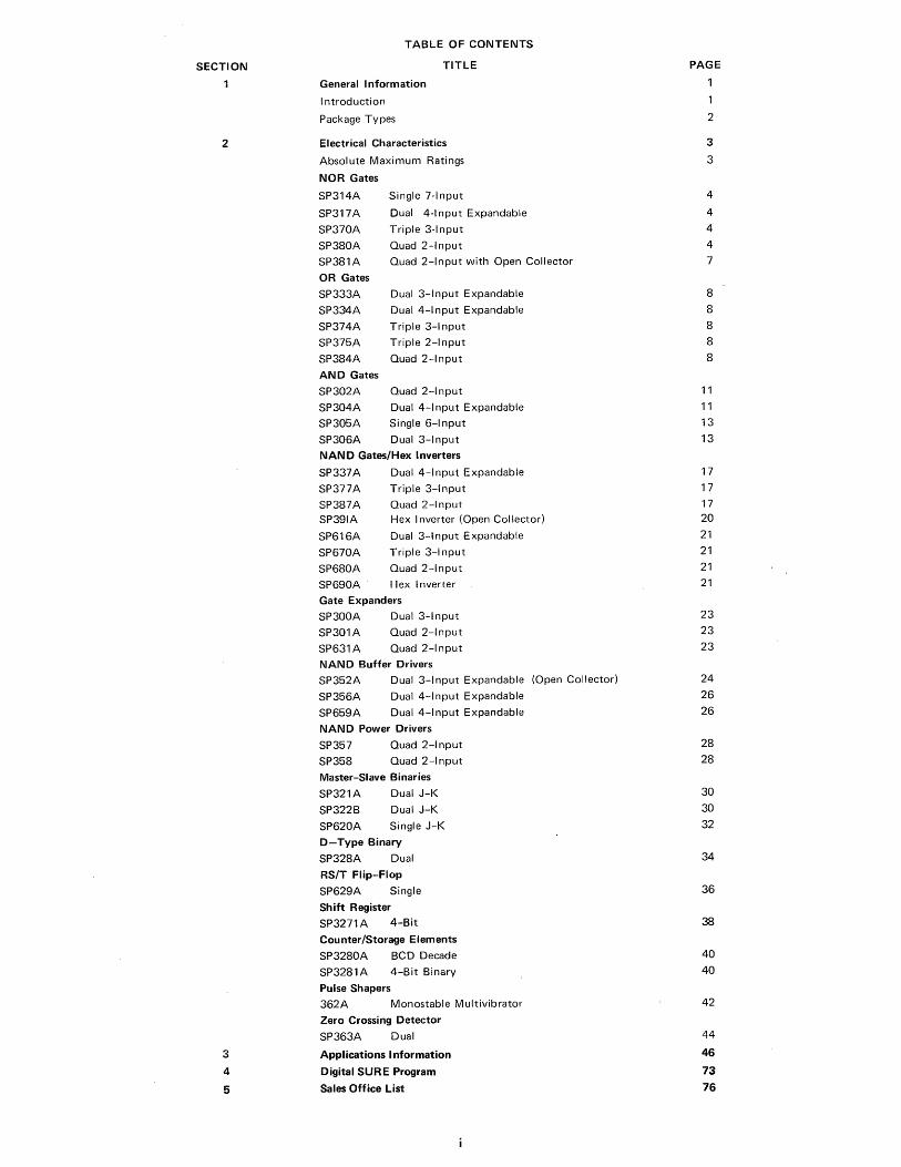
TABLE OF CONTENTS
SECTION TITLE PAGE
General Information
Introduction
Package Types 2
2 Electrical Characteristics 3
Absolute Maximum Ratings 3
NOR Gates
SP314A Single 7-1 nput 4
SP317A Dual 4-1 nput Expandable 4
SP370A Triple 3-1 nput 4
SP380A Quad 2-lnput 4
SP381 A Quad 2-lnput with Open Collector 7
OR Gates
SP333A Dual 3-lnput Expandable 8
SP334A Dual 4-1 nput Expandable 8
SP374A Triple 3-1 nput 8
SP375A Triple 2-lnput 8
SP384A Quad 2-lnput 8
AND Gates
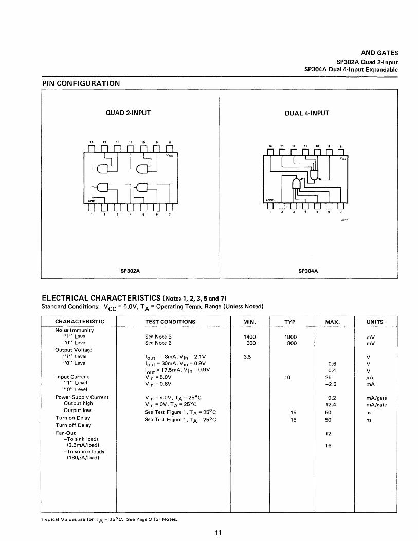
SP302A Quad 2-lnput 11
SP304A Dual 4-1 nput Expandable 11
SP305A Single 6-1 nput 13
SP306A Dual 3-1 nput 13
NAND Gates/Hex Inverters
SP337A Dual 4-1 nput Expandable 17
SP377A Triple 3-1 nput 17
SP387A Quad 2-lnput 17
SP391A Hex Inverter (Open Collector) 20
SP616A Dual 3-1 nput Expandable 21
SP670A Triple 3-1 nput 21
SP680A Quad 2 -I nput 21
SP690A Hex Inverter 21
Gate Expanders
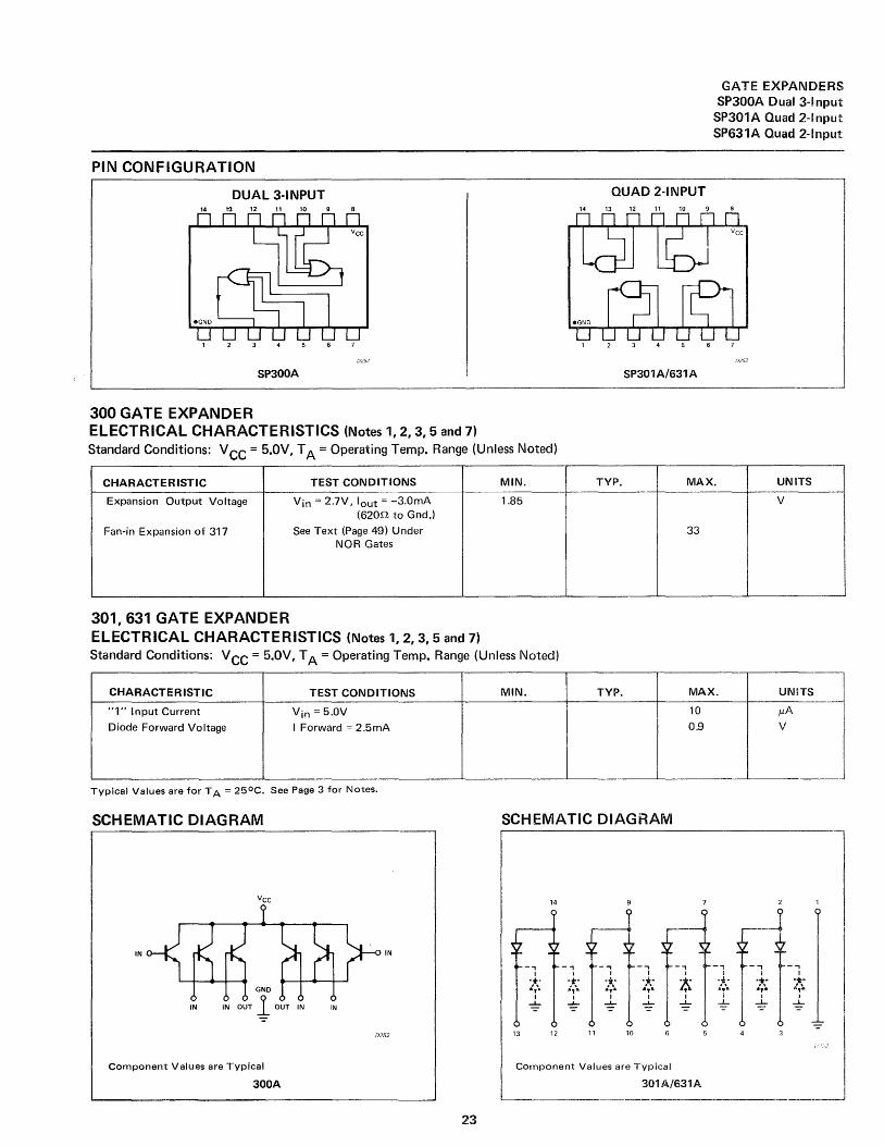
SP300A Dual 3-1 nput 23
SP301A Quad 2-1 nput 23
SP631A Quad 2-1 nput 23
NAND Buffer Drivers
SP352A Dual 3-1 nput Expandable (Open Collector) 24
SP356A Dual 4-1 nput Expandable 26
SP659A Dual 4-1 nput Expandable 26
NAND Power Drivers
SP357 Quad 2-lnput 28
SP358 Quad 2-1 nput 28
Master-Slave Binaries
SP321A Dual J-K 30
SP322B Dual J-K 30
SP620A Single J-K 32
D-Type Binary
SP328A Dual 34
RS/T Flip-Flop
SP629A Single 36
Shift Register
SP3271A 4-Bit 38
Counter/Storage Elements
SP3280A BCD Decade 40
SP3281A 4-Bit Binary 40
Pulse Shapers
362A Monostable Multivibrator 42
Zero Crossing Detector
SP363A Dual 44
3 Applications Information 46
4 Digital SURE Program 73
5 Sales Office List 76
Copyright 1972
SIGNETICS CORPORATION
Signetics Corporation reserves the right to make changes in the products contained in this book in order to improve design or performance and to supply the best possible product.
Signetics Corporation assumes no responsibility for the use of any circuits described herein and makes no representations that they are free from patent infringement.
o 25% to 50% recycled paper
ii
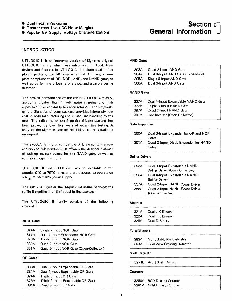
• Dual In-Line Packaging • Greater than '-volt DC Noise Margins • Popular 5V Supply Voltage Characterizations
INTRODUCTION
UTI LOGIC II is an improved version of Signetics original UTI LOGIC family which was introduced in 1964. New devices and features in UTI LOGIC II include dual in-line plug-in package, two J-K binaries, a dual D binary, a complete complement of OR, NOR, AND, and NAND gates, as well as buffer line drivers, a one shot, and a zero crossing detector.
The proven performance of the earlier UTI LOG IC family, including greater than 1 volt noise margins and high capacitive drive capability has been retained. The simplicity of the Signetics silicone package provides inherently low cost in both manufacturing and subsequent handling by the user. The reliability of the Signetics silicone package has been proved by over five years of exhaustive testing. A copy of the Signetics package reliability report is available on request.
The SP600A family of compatible DTL elements is a new addition to this handbook. It affords the designer a choice of pull-up resistor values for the NAND gates as well as additional logic functions.
UTI LOGIC II and SP600 elements are available in the popular O°C to 75°C range and are designed to operate on a V cc = 5V ±10% power supply.
The suffix A signifies the 14-pin dual in-line package; the suffix B signifies the 16-pin dual in-line package.
The UTI LOGIC II family consists of the following elements:
NOR Gates
314A 317A 370A 380A 381A
OR Gates
333A 334A 374A 375A 384A
Single 7-lnput NOR Gate Dual 4-lnput Expandable NOR Gate Triple 3-lnput NOR Gate Quad 2-lnput NOR Gate Quad 2-lnput NOR Gate (Open-Collector)
Dual 3-lnput Expandable OR Gate Dual 4;.Jnput Expandable OR Gate Triple 3-lnput OR Gate Triple 2-lnput Expandable OR Gate Quad 2-lnp'ut OR Gate
1
AND Gates
302A 304A 305A 306A
Section General Information
Quad 2-lnput AND Gate Dual 4-lnput AND Gate (Expandable) Single 6-lnput AND Gate Dual 3-lnput AND Gate
NAND Gates
337A Dual 4-lnput Expandable NAND Gate 377A Triple 3-lnput NAND Gate 387A Quad 2-lnput NAND Gate 391A Hex Inverter (Open Collector)
Gate Expanders
300A Dual 3-lnput Expander for OR and NOR Gates
301A Quad 2-lnput.Diode Expander for NAND Gates
Buffer Drivers
352A
356A
357A 358A
Binaries
321A 322A 328A
Dual 3-1 nput Expandable NAN D Buffer Driver (Open Collector)
Dual 4-lnput Expandable NAND Buffer Driver Quad 2-lnput NAND Power Driver Quad 2-lnput NAND Power Driver ( Open-Collector)
Dual J-K Binary Dual J-K Binary Dual D Binary
Pulse Shapers
362A I Monostable Multivibrator 363A Dual Zero Crossing Detector
Shift Register
I 3271 B I 4-Bit Shift Register
Counters
3280A I BCD Decade Counter 3281A 4-Bit Binary Counter
The SP600 family consists of the following elements:
NAND Gates
616A 670A 680A
Dual 4-lnput Expandable NAND Gate Triple 3-lnput NAND Gate Quad 2-lnput NAND Gate
Line Driver
659A I Dual 4-1 nput Buffer/Driver
J-K Binary
620A I Single J-K Binary
RS/T Binary
629A I Single RS/T Binary
Inverter
690A Hex Inverter
Expander
631 A I Gate Expander
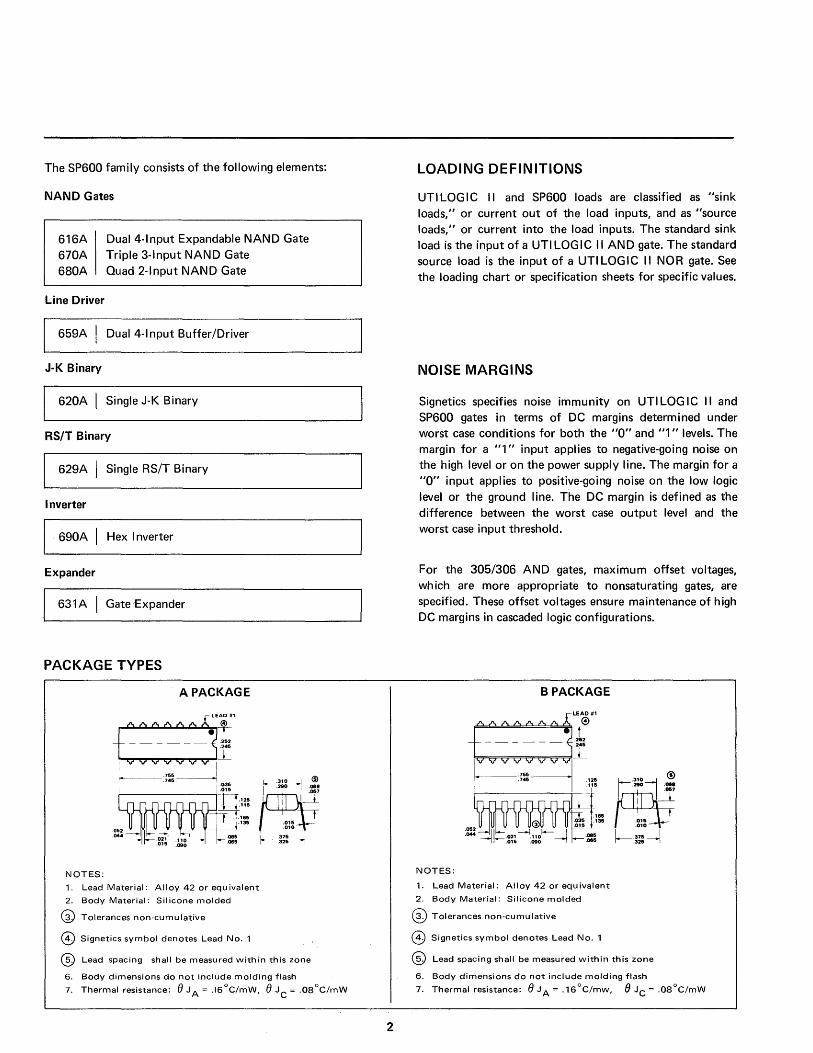
PACKAGE TYPES
A PACKAGE
f~ ~:-:-:-:~~¥ , .756 v- v- v- I
i .7.5~ r---_____ ---;l :~~
-[1-'25 .115
I~r !.'85 I _~135
.085 ------ .066
NOTES:
1. Lead Material: Alloy 42 or equivalent
2. Body Material: Silicone molded
@ Tolerances non-cumulative
@ Signetics symbol denotes Lead No.1
® Lead spacing shall be measured within this zone
6. Body dimensions do not include molding flash
7. Thermal resistance: e J A = .16°C/mW, e JC
= .08°C/mW
2
LOADING DEFINITIONS
UT I LOG I C II and SP600 loads are classified as "si nk loads," or current out of the load inputs, and as "source loads," or current into the load inputs. The standard sink load is the input of a UTI LOG I C II AN D gate. The standard source load is the input of a UTILOGIC II NOR gate. See the loading chart or specification sheets for specific values.
NOISE MARGINS
Signetics specifies noise immunity on UTI LOG IC II and SP600 gates in terms of DC margins determined under worst case conditions for both the "0" and "1" levels. The margin for a "1" input applies to negative-going noise on the high level or on the power supply line. The margin for a "0" input applies to positive-going noise on the low logic level or the ground line. The DC margin is defined as the difference between the worst case output level and the worst case input threshold.
For the 305/306 AND gates, maximum offset voltages, which are more appropriate to nonsaturating gates, are specified. These offset voltages ensure maintenance of high DC margins in cascaded logic configurations.
NOTES:
BPACKAGE
f:~ ~:: ~ ~?" I
.766·~
.746 .• 26 .115
~IU ~1.'86 r.:. .035 .'35 \!I .015
.052 I I-- 1
.0« -=11_ .02' -.11 0 _I _ .085 .0.5 .090 ~ .085
1. Lead Material: Alloy 42 or equivalent
2. Body Material: Silicone molded
o Tolerances non-cumulative
@ Signetics symbol denotes Lead No.1
@ Lead spacing shall be measured within this zone
6. Body dimensions do not include molding flash
7. Thermal resistance: e J A = .16°C/mw, e J C = .08°C/mW
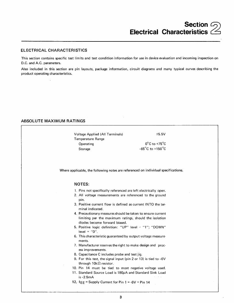
ELECTRICAL CHARACTERISTICS
Section Electrical Characteristics
This section contains specific test limits and test condition information for use in device evaluation and incoming inspection on
D.C. and A.C. parameters.
Also included in this section are pin layouts, package information, circuit diagrams and many typical curves describing the product operating characteristics.
ABSOLUTE MAXIMUM RATINGS
Voltage Applied (All Terminals)
Temperature Range
Operating
Storage
±5.5V
O°C to +75°C
-65°C to +150°C
Where applicable, the following notes are referenced on individual specifications.
NOTES:
1. Pins not specifically referenced are left electrically open. 2. All voltage measurements are referenced to the ground
pin. 3. Positive current flow is defined as current I NTO the ter
minal indicated. 4. Precautionary measures should be taken to ensure current
limiting per the maximum ratings, should the isolation diodes become forward biased.
5. Positive logic definition: "UP" level = "1"; "DOWN" level = "0".
6. This characteristic guaranteed by output voltage measurements.
7. Manufacturer reserves the right to make design and process improvements.
8. Capacitance C includes probe and test jig. 9. For this test, the signal input (pin 2 or 13) is tied to -6V
th rough 10kD. resistor. 10. Pin 14 must be tied to most negative voltage used. 11. Standard Source Load is 180}1A and Standard Sink Load
is -2.5mA
12. lEE = Supply Current for Pin 1 = -6V = Pin 14
3
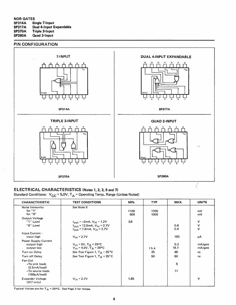
NOR GATES SP,314A Single 7-lnput SP317A Dual4·lnput Expandable SP370A Triple 3·1 nput SP380A Quad 2-lnput
PIN CONFIGURATION
7-INPUT DUAL 4·INPUT EXPANDABLE
14 13 12 11 10 14 13 12 11 10
SP314A SP317A
TRIPLE 3-INPUT QUAD 2·INPUT
14 13 12 11 10 14 13 12 11 10
SP370A SP380A
ELECTRICAL CHARACTERISTICS (Notes 1,2,3,5 and 7) Standard Conditions: V CC = 5.0V, T A = Operating Temp. Range (Unless Noted)
CHARACTERISTIC TEST CONDITIONS MIN. TYP MAX. UNITS
Noise Immunity See Note 6 for "1" 1100 1700 mV for "0" 600 1000 mV
Output Voltage "1" Level lout = -2mA, Vin = 1.2V 3.8 V "0" Level lout = 12.5mA, Vin = 2.7V 0.6 V
lout = 7.5mA, Vin = 2.7V 0.4 V
Input Current -input high Vin = 2.7V 180 J..LA
Power Supply Current output high Vin=OV,TA=25°C 0.3 mA/gate output low Vin = 4.0V, TA = 25°C 13.4 18.1 mA/gate
Turn on Delay See Test Figure 1, T A = 25°C 25 60 ns
Turn off Delay See Test Figure 1, T A = 25°C 50 80 ns
Fan·Out -To sink loads 5
(2.5mA/load) -To source loads 11
(180J..LA/load)
Expander Voltage Vin = 2.7V 1.85 V (317 only)
Typical Values are for T A = 250 C. See Page 3 for Notes.
4
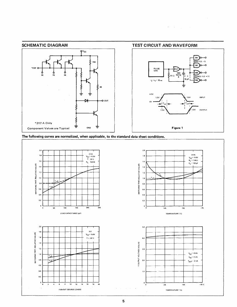
SCHEMATIC DIAGRAM
740
*EXP ~-+----6-~--~~~--~-. __ ~
IN IN IN
40
... ----011-----+--0 OUT
*317 A Only
Component Values are Typical GND
TEST CIRCUIT AND WAVEFORM
~ I SINK F.O. = 5
PULSE GEN
5Hl.
40V I
15V 15V
OV I I I
INPUT
-:'t -:'7 I I I 1 5V 1 5V OUTPUT
I I
Figure 1
The following curves are normalized, when applicable, to the standard data sheet conditions.
2.0
317A -VCC= +5.0V
1.8
T = 25c C 1.6
RL = NONE
1.4
~ -.......
./ V 1 o!!., -.:? ~
1.2
1.0
0.8
"'P' / 0.6
/ 0.4
0.2
50 100 150 200 250
LOAD CAPACITANCE (pF)
2.0 I ,
iii 1.8
3 317 -
VCC= +5.0V
<t 1.6 > T = +25"C w >
~ 1.4
1.2 :;; i= .-V ~
I-""
<:l 1.0 z
~ 0.8
~
~ ~ t::-!=---
~p
0.6
0.4
0.2
o o 10 12 14 16 18 20
FAN.OUT (SOURCE L.OADSi
5
2.0 I
317A -1.8 VCC= +5.0V
1.6 RL = 1.6K!! -
\ CL = 130 pF
'" P ,---1 off ~ -~ ~~
1.4
1.2
1.0 -0.8
0.6
0.4
0.2
o o +25 +50 +75
5.0 ....------r-----T"""----.,.-------.-----.,-----,
4.0 I---
3.0 1---+-------I----I---+---4-----l
2.0 1---+------1----1---+
VCC= +5.0V
V'N= +1.2V
10UT
=·2 mA -
1.0 1---+------I----I---+---4-----l
0L----~----+-------+-------~----~----~ o +25 +50 +75"C
TEMPERATURF lOCi
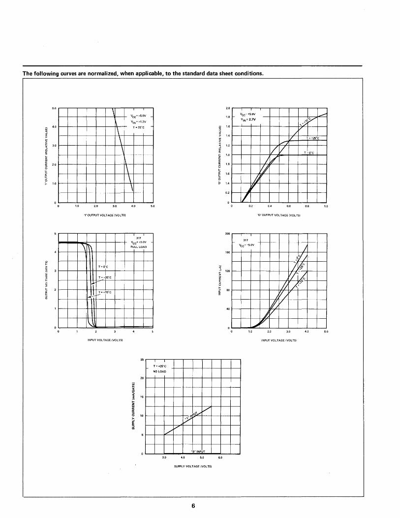
The following curves are normalized, when applicable, to the standard data sheet conditions.
5.0
\ I
vee= +5.0V -
1\ V1N = +1.2V
\ T = 25'e -
\ \
\
\ \ \
4.0
3.0
2.0
1.0
o
2.0
1.8
W 1.6
3 q:
1.4 > > >=
1.2 i f- 1.0
~ 1.8 a f-
~ 1.6
0
9 1.4
0.2
I I I
- Vee= +5.0V .......... VIN = 2.7V
~ ,1 ... '
/V ~ T = +25'e
rl 1/ V T !o'e
/ V Ij
fj~
~,.
IL o o 1.0 2.0 3.0 4.0 5.0 o 0.2 0.4 0.6 0.8 1.0
'I' OUTPUT VOLTAGE (VOLTS) '0' OUTPUT VOL TAGE (VOLTS)
I I 200 I
317
Vee= +5.0V -
\ '" FULL LOAD
160
I-317
Vee= +5.0V
L ,ill
T =o'e
T = +~5'e r
fA LL.-! = +75'e
1 120 f-z w a: a: a f-:::J 80 ~
)'Mv v, · If"
II A:-",'
/,'1/
40 ~/
~ '/ , ~ ~
1.0 2.0 3.0 4.0 50
INPUT VOL TAGE (VOLTS) INPUT VOLTAGE (VOLTS)
25 I I
l-T = +25'e
NO LOAD
20
W ~ !2 «
15 ..s I-
ffi a: a: ;:) (,) 10 > t
~-.)~ /
" ,'I'
~ ;:) en
./ ./'"
"0" INPUT
3.0 4.0 5.0 6.0
SUPPLY VOLTAGE (VOLTS)
6
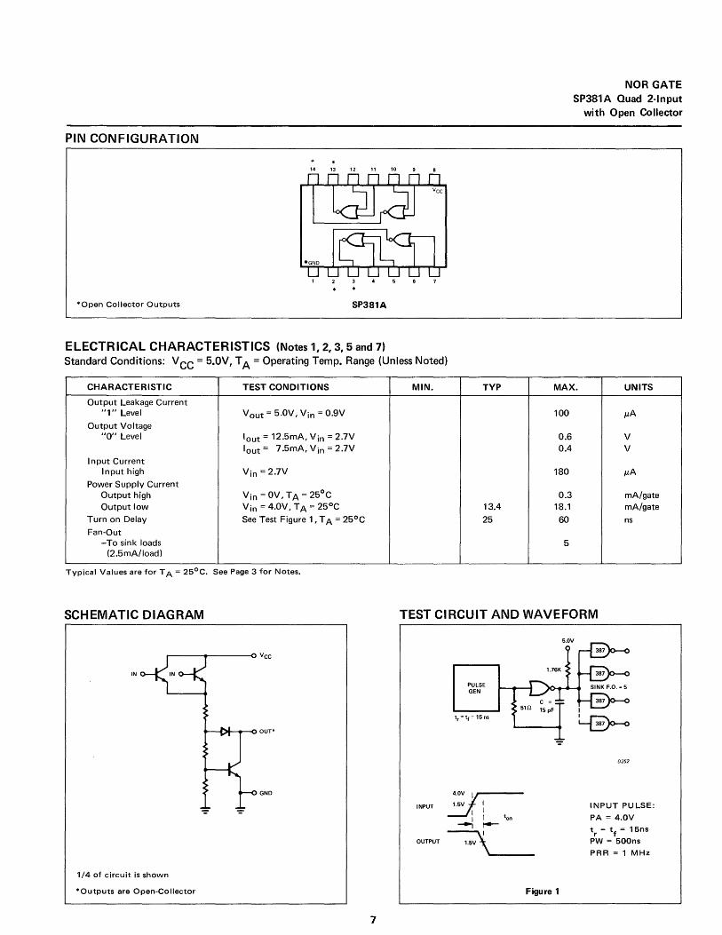
PIN CONFIGURATION
14 13 12 11 10
* Open Collector Outputs SP381A
ELECTRICAL CHARACTERISTICS (Notes 1,2,3,5 and 7)
NOR GATE SP381A Quad 2-lnput
with Open Collector
Standard Conditions: V CC = 5.0V, T A = Operating Temp. Range (Unless Noted)
CHARACTERISTIC TEST CONDITIONS
Output Leakage Current "1" Level V out = 5.0V, Vin = 0.9V
Output Voltage "0" Level lout = 12.5mA, Vin = 2.7V
lout = 7 .5mA, Vin = 2.7V
Input Current Input high Vin = 2.7V
Power Supply Current Output high Vin =OV, TA = 25°C Output low Vin = 4.0V, TA = 25°C
Turn on Delay See Test Figure 1, T A = 25°C
Fan-Out -To sink loads
(2.5mA/load)
Typical Values are for T A = 25°C. See Page 3 for Notes.
SCHEMATIC DIAGRAM
r----_---oO vcc
IN
..-~ ....... _OOUT·
GND
1/4 of circuit is shown
*Outputs are Open-Collector
7
MIN. TYP MAX. UNITS
100 JlA
0.6 V 0.4 V
180 JlA
0.3 rnA/gate 13.4 18.1 mA/gate
25 60 ns
5
TEST CIRCUIT AND WAVEFORM
PULSE GEN
t, = tf = 15 n5
INPUT ~::~ r,--.:::..II! t I I ton ~ t4-
OUTPUT~
Figure 1
0252
INPUT PULSE:
PA = 4.0V
\ = t f = 15ns
PW = 500ns PRR = 1 MHz
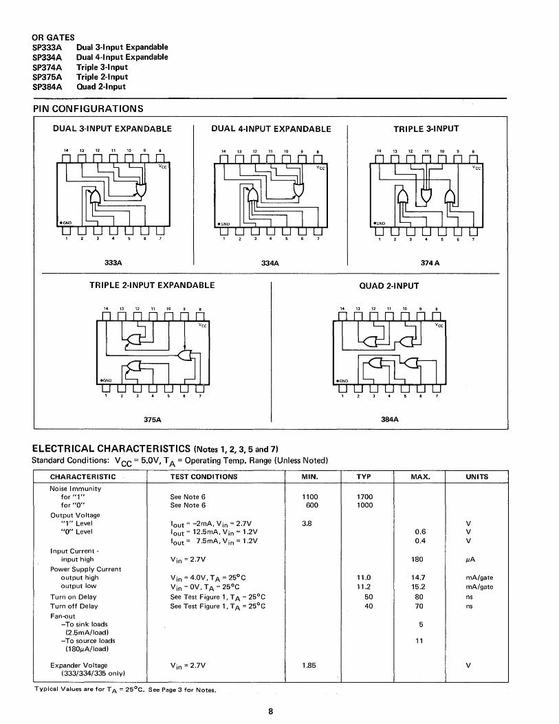
OR GATES SP333A SP334A SP374A SP375A SP384A
Dual 3-lnput Expandable Dual 4-1 nput Expandable Triple 3-lnput Triple 2-lnput Quad 2-lnput
PIN CONFIGURATIONS
DUAL 3-INPUT EXPANDABLE DUAL 4-INPUT EXPANDABLE
14 13 12 11 10 14 13 12 11 10
333A 334A
TRIPLE 2-INPUT EXPANDABLE
14 13 12 11 10
375A
ELECTRICAL CHARACTERISTICS (Notes 1,2,3,5 and 7) Standard Conditions: V CC = 5.0V, T A = Operating Temp. Range (Unless Noted)
CHARACTERISTIC TEST CONDITIONS MIN.
Noise Immunity for "1" See Note 6 1100 for "0" See Note 6 600
Output Voltage "1" Level lout = -2mA, Vin = 2.7V 3.8 "0" Level lout = 12.5mA, Vin = 1.2V
lout = 7 .5mA, Vin = 1.2V
Input Current -input high Vin = 2.7V
Power Supply Current output high Vin = 4.0V, TA = 25°C output low Vin=OV,TA=25OC
Turn on Delay See Test Figure 1, T A = 25°C Turn off Delay See Test Figure 1, T A = 25°C
Fan-out -To sink loads
\
(2.5mA/load) -To source loads
(180p,A/load)
Expander Voltage Vin = 2.7V 1.85 (333/334/335 only)
Typical Values are for T A = 25°C. See Page 3 for Notes.
8
TRIPLE 3-INPUT
14 13 12 11 10
374 A
QUAD 2-INPUT
14 13 12 11 10
384A
TVP MAX. UNITS
1700 1000
V 0.6 V 0.4 V
180 p,A
11.0 14.7 mA/gate 11.2 15.2 mA/gate
50 80 ns 40 70 ns
5
11
V
SCHEMATIC DIAGRAM
*EXP
Component Values are Typical
*333/334/374 Only
OUT
TEST CIRCUIT AND WAVEFORM.
PULSE GEN
51.(2
rE»-o I SINK F.O. = 5
c= I 15PF~=11
L-______ ~ ~
4.0V I 1.5V I 1.5V INPUT
OV I I I --*i T off f4- -.l Ton 14-
'!'5:··~ 1.5V OUTPUT
~ ~
Figure 1
The following curves are normalized, when applicable, to the standard data sheet conditions.
2.0 I I 200
333 Vce= +5.0V -
T = +25'C
I- 333
VCC= +5.0V
1.8 180
RL = 1.6K --- I---- -I--
~~ ~~
V" /? '"
v./
l- T = +25'C V
RL = 1.6K / I- CL = 130 pF V ~
V
V /'
V
V -:7 Toft
1.6
1.4
1.2
1.0
0.8
0.6
0.4
160
140
120
100
80
60
40
0.2 20
o o o 100 200 300 400 500 o 10 20 30 40 50 60 70 80 90 100
LOAO CAPACITANCE (pF) EXPANSION INPUT CAPACITANCE (pF)
9
00 ~----~I----T-----~----~----~--~
f-- Vee::~.OV 40 f-- e L = 130 pF
RL = 1.6K to GND.
Toft -
20 ~----+-----+-----+-----+-----+---~
10~----+-----+-----+-----+-----+---~
o~----~----~----~----~----~--~ o +25 +00 +75
0252
200~~1~-~1--~~--~--~--~--T---~~
333
1.0 2.0 3.0 4.0 5.0
INPUT VOLTAGE (VOLTS)
0252
r-
o o
25
20
15
10
10
I 333 I
Vee= +5.0V
FULL LOAD (
I T =ooe
"'" 1 ° ,_y+~5 e
V+75oe
j ....J.
INPUT VOLTAGE (VOLTS)
0252
II T = +25°e
...... "~~~~ ::"... "o"\~
~ ~
3.0 4.0 5.0 6.0
SUPPL Y VOLT AG E (VOLTS)
0252
PIN CONFIGURATION
QUAD 2-INPUT
14 13 12 11 10
SP302A
ELECTRICAL CHARACTERISTICS (Notes 1,2,3,5 and 7) Standard Conditions: V CC ::: 5.0V, T A ::: Operating Temp. Range (Unless Noted)
CHARACTERISTIC TEST CONDITIONS MIN.
Noise I rnmunity "1" Level See Note 6 1400 "0" Level See Note 6 300
Output Voltage "1" Level lout = -3mA, Vin = 2.1V 3.5 "0" Level lout = 30mA, Vin = 0.9V
lout = 17.5rnA, Vin = 0.9V Input Current Vin = 5.0V
"1" Level Vin = 0.6V "0" Level
Power Supply Current Vin = 4.0V, TA = 25°C Output high Vin=OV,TA=25°C Output low See Test Figure 1, T A = 25°C
Turn on Delay See Test Figure 1, T A = 25°C Turn off Delay
Fan-Out -To sink loads
(2.5rnA/load) -To source loads
(180JlA/load)
Typical Values are for T A = 25°C. See Page 3 for Notes.
11
AND GATES
SP302A Quad 2-1 nput SP304A Dual 4-lnput Expandable
DUAL 4-INPUT
14 13 12 11 10
0252
SP304A
TYP. MAX. UNITS
1800 rnV 800 mV
V 0.6 V 0.4 V
10 25 JlA -2.5 rnA
9.2 rnA/gate 12.4 rnA/gate
15 50 ns
15 50 ns
12
16
SCHEMATIC DIAGRAM
2.5K
Component Values are Typical
1/4 of circuit shown
TEST CIRCUIT
1Kn
PULSE o-__ ~+--~ 13 IN
51n
12
11
10
SP302A
5.0V
Vcc
Vcc
Boon 2K 150n
':" 0252
c=~ ~'" t ~ oOS.OV
SCHEMATIC DIAGRAM
2.5K
Component Values are Typical
1/2 of circuit is shown
TEST CIRCUIT
PULSE IN
1Kn
SP304A
11
14
14~""'_<T
GND
All diodes are 1 N916's SP302A
WAVEFORM
INPUT PULSE
PA = 4.0V
tr = tf = 10nsec
PW = 500nsec
PR R = 1 MHz
r;'~ 0252
All diodes are 1 N916's SP304A
-1Tt[ JTrr-
~0"10 ±fi----90% -1W lW
10"10 10"10
OV To~~ I - '~rr Vv 1.51
INPUT
OUTPUT
12
Vcc
Boon 2K 150n
":'" 0252
PIN CONFIGURATION
SINGLE 6-INPUT
14 13 12 11 10
0252
305A
ELE,CTRICAL CHARACTERISTICS (Notes 1, 2, 3, 5 and 7)
DUAL 3-1 NPUT
14 13 12 11 10
306A
AND GATES SP305A Single 6-1 nput
SP306A Dual 3-lnput
Standard Conditions: VCC = 5.0V, T A = Operating Temperature Range (Unless Noted)
CHARACTERISTIC TEST CONDITIONS MIN. TYP. MAX. UNITS
Offset Voltage "1" Level lout = -1.8mA, Vin = 3.8V 0.15 V
measure Vin - Vout "0" Level lout = 0, Vin = 0.6V -0.3 V
measure Vin - V out Input Current
input high Vin = 5.0V 10 40.0 J,lA input low Vin = 0.6V -2.5 mA
Power Supply Current Vin = 4.0V, TA = 25°C output high 0.9 rnA/gate
output low Vin = OV, T A = 25°C 2.9 rnA/gate
Turn on Delay See Test Figure 1, T A = 25°C 15 50 ns Turn off Delay See Test Figure 1, T A = 25°C 32 60 ns
Fan-out -To sink loads 0
(2.5rnA/load) -To source loads 10
(180J,lA/load)
Typical Values are for T A = 25°C. See Page 3 for Notes.
13
SCHEMATIC DIAGRAM
Component Values are Typical
TEST CIRCUIT AND WAVEFORM
PULSE
GEN
'IN
IN
IN
0252
....-----__ 0 Vcc
2K
OUT
GND
0252
Figure 1
4'OV~ 1.5V I 1.5V
OV I I I INPUT
-.JToff~ -../Ton~
~II
I ' 1.5V I 1.5V
I I OUTPUT
0252
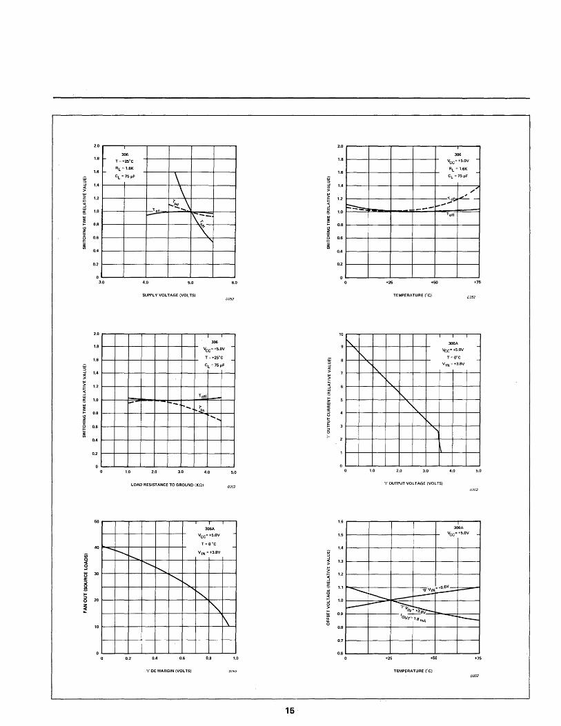
The following curves are normalized, when applicable, to the standard data sheet conditions.
2.0
/V
/'
/ 306
Vce= 5.0V -
/ T = +25°C
V RL = 1.6K -
/ -<'0" ;i.fo~
-~ .... /
./V V
1.8
1.6
1.4
1.2
1.0
0.8
0.6
0.4
2.0 I I
VCC= +5.0V
_ T = +25°C ~
V ...... /~
,/
~ .y
.... ~ ~ I---r--"Io~
~, ~ C; v
1.8
1.6
1.4
1.2
1.0
0.8
0.6
0.4
0.2 0.2
o o o 20 40 60 80 100 120 140 160 180 200 o 10 12 14 16 18 20
LOAD CAPACITANCE - (pF) D252 FAN OUT (SOURCE LOADS)
D252
14
~ « > w >
i w ::;; >= t:l z i ~ ~
W 3 « > w >
i w ::;; >= t:l Z i ~ ~
iii Q « 9 w CJ rr: ;:, 0 !!! ... ;:, 0 Z
~
2.0
1.8 r-
1.6 r-
1.4
1.2
1.0
0.8
0.6
0.4
0.2
o 3.0
2.0
1.8
1.6
1.4
1.2
1.0
O.S
0.6
0.4
0.2
0 0
50
40
30
20
10
o o
306
T = +25°C
RL = 1.6K
CL = 75 pF \ \
"on r!~ .... \ - 1\.:-
\ ......
4.0 5.0 6.0
SUPPLY VOLTAGE (VOLTS) 0252
I
306
VCC= +5.0V -
T = +25°C _
CL = 75 pF
-- --I'- ....
........
1.0 2.0 3.0 4.0 5.0
LOAD RESISTANCE TO GROUND (Kn) 0252
I I I
306A
VCC= +5.0V -T=O°C -..... 1'--..
.......... VIN = +3.8V
........... r--..... ~ r--...
" I'\. \
0.2 0.4 0.6 0.8 1.0
'I' DC MARGIN (VOLTS)
16
W 3 « > w > >=
i w ::;; >= t:l z i ~ ~
~ « > >
i ... z w
"' "' :::> u ... ~ :::> o
W 3 « > w > >=
i w t:l
~ 0 > ... w (I) u.
~
2.0
1.8
1.6
1.4
1.2
1.0
0.8
0.6
0.4
0.2
0
10
o
1.6
1.5
1.4
1.3
1.2
1.1
1.0
0.9
0.8
0.7
0.6
306
VCC= +5.0V -
RL = 1.6K _
CL = 75 pF
","
r-----+-----+-----+-----~~~?~~ ---- .... --~
0 +25 +50 +75
TEMPERATURE (oC) 0252
I I I
~ 306A -"'~
VeC= +5.0V
T= DOe -"r'\..
Y,N = +3.8V
" " ',-'t'...
"'\ "-
"\
o 1.0 2.0 3.0 4.0 5.0
'I' OUTPUT VOLTAGE (VOLTS)
n252
306A
VCC= +5.0V -
'O'V\N~ ............... t--
"-.... --------~ ~~ I ~8v OUT~ 7.8"'4 -I---
o +25 +50 +75
TEMPERATURE (OC) 0252
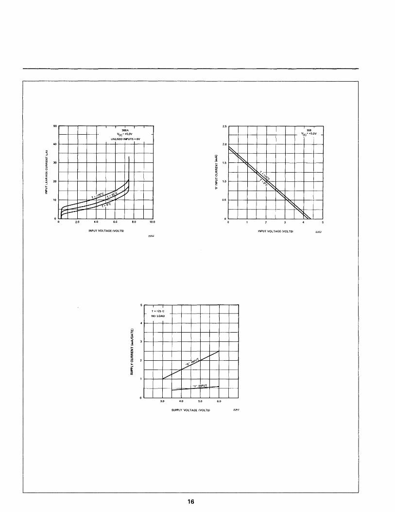
50 I I 2.5
306A 306 Vee: +5.0V Vee= +5.0V -
UNUSED INPUTS: OV
40 2.0
1 l-
i 30
a w C>
~ ~ 20
I-
~ ~
10
/~ ~~ ~~~
~ I--~ Kfc r ~
~ E
1.5 I-z II: II: ::> (.)
I-
~ 1.0
?
0.5
~ "~ ~ ~ )'>$'0
)0 C'
~'~ Oc-t-..
~~ ~ ~
F ~"""" o '\:: ~ o
o 2.0 4.0 6.0 8.0 10.0 o
INPUT VOL TAGE (VOLTS) INPUT VOL TAGE (VOLTS)
0252
I I
T = +25 e I-
NO LOAD
,,/ /"
~..:J'" "'Y ./
./ ,,/
"1" INPUT -3.0 4.0 5.0 6.0
SUPPLY VOLTAGE (VOLTS) 0252
16
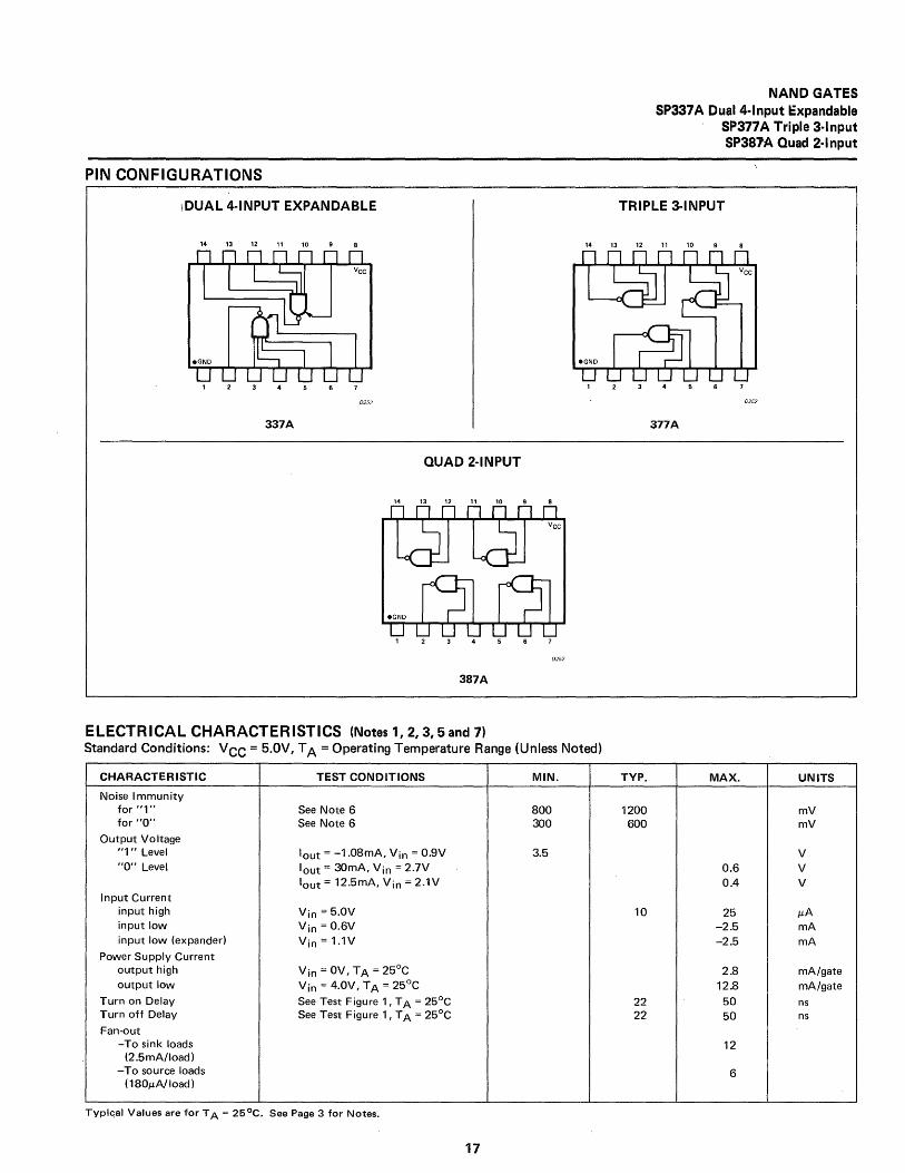
PIN CONFIGURATIONS
\DUAL 4·INPUT EXPANDABLE
14 13 12 11 10
0252
337A
QUAD 2·INPUT
14 13 12 11 10
387A
ELECTRICAL CHARACTERISTICS (Notes 1,2,3,5 and 7)
NAND GATES SP337A Dual4·lnput Expandable
SP377A Triple 3·lnput SP387A Quad 2·lnput
TRIPLE 3·INPUT
14 13 12 11 10
0252
377A
Standard Conditions: VCC = 5.0V, T A = Operating Temperature Range (Unless Noted)
CHARACTERISTIC TEST CONDITIONS MIN. TYP. MAX. UNITS
Noise Immunity for "1" See Note 6 BOO 1200 mV for "0" See Note 6 300 600 mV
Output Voltage "1" Level lout = -1.0BmA, Vin = 0.9V 3.5 V "0" Level lout = 30mA, Vin = 2.7V 0.6 V
lout = 12.5mA, Vin = 2.1V 0.4 V Input Current
input high Vin = 5.0V 10 25 }.LA input low Vin = 0.6V -2.5 rnA input low (expander) Vin=1.1V -2.5 mA
Power Supply Current output high Vin = OV, T A = 25°C 2.B mA/gate output low Vin = 4.0V, TA = 25°C 12.B mA/gate
Turn on Delay See Test Figure 1, T A = 25°C 22 50 ns Turn off Delay See Test Figure 1, T A = 25°C 22 50 ns Fan-out
-To sink loads 12 (2.5mA/load)
-To source loads 6 (1BO}.LA/load)
Typi<;al Values are for T A = 25°C. See Page 3 for Notes.
17
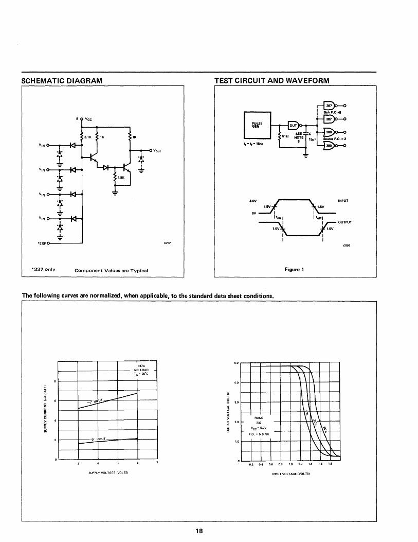
SCHEMATIC DIAGRAM
1K
t--t--oVout I ••• . ,. I
* VIN
I ••• ·r\
* VIN I .,. .,\
* *EXP
*337 only Component Values are Typical
0252
TEST CIRCUIT AND WAVEFORM
r-Go--o ~ Sinlc F.O.-8
PULSE GEN
387
4.0V INPUT
1.5V 1.5V
OV I I I tan I , tort,
I OUTPUT
1.5V 1.5V
I I I I
0252
Figure 1
The following curves are normalized, when applicable, to the standard data sheet conditions.
I 5.0 337A
NO LOAD - "'\. ~ ........ TA • 25°e , \ 1\
\ 4.0
~~~ -~
"0" INPUT
~
\ \ \ \ \
NAND f \ - 337
\ I\~
Vee· 5.0V '( ~~o r-,... F.O .• 5 SINK ~\ '\-
\ \\
3.0
2.0
1.0
~ ~ 0.2 0.4 0.6 0.8 1.0 1.2 1.4 1.6 1.8
SUPPLY VOLTAGE (VOLTS) INPUT VOLTAGE (VOLTS)
18
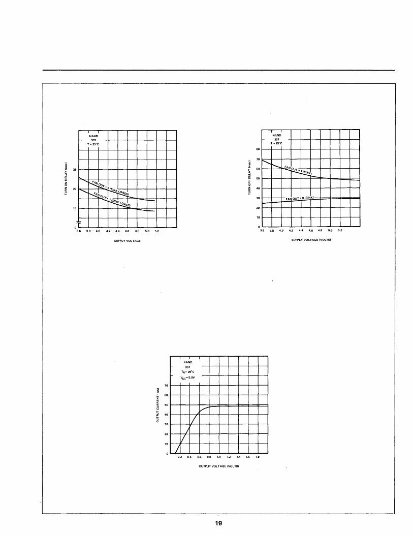
I I I
NAND NAND
I- 337 I- 337
T; 25°C T = 25°C
80
I 25 >
~ 0 z 0
~ 20
...
15
........ ~ "'~8
............ J~ ~", ( 0408) °U.,. ........ ~~I(( J --
~8) r---
70
I 60 >
~ 0 50
q
~ 40
30
20
r---.... ........... F~OU"'~7 ~~I-
fAN OUT = 8 (SINK) -10
~~ o o u u u u u u u u u U U U U U U U U U
SUPPL Y VOL T AGE SUPPLY VOL TAGE (VOLTS)
I T I NAND
I- 337
TA= 25°C
Vee= 5.0V
70
<" E
60 ... z a: a: 50 a ... / ~ 40
0 30
/ 20
10
J V
/ 0.2 0.4 0.6 0.8 1.0 1.2 1.4 1.6 1.8
OUTPUT VOL TAGE (VOLTS)
19
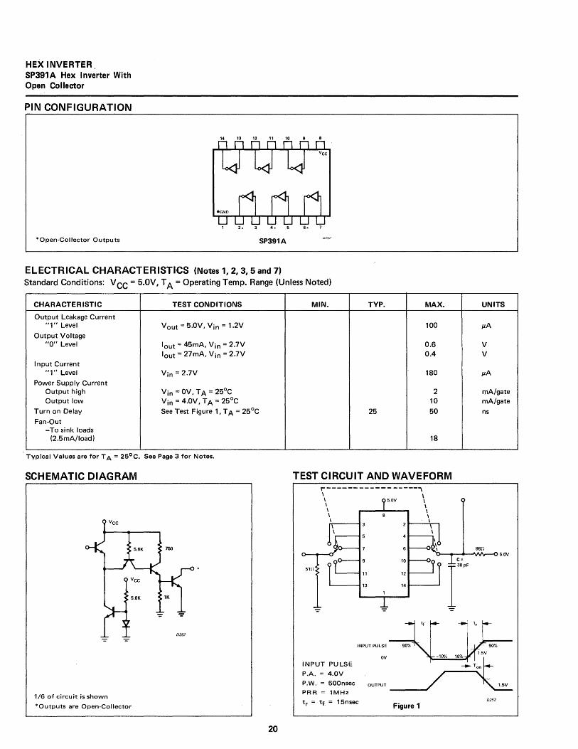
HEX INVERTER, SP391A Hex Inverter With Open Collector
PIN CONFIGURATION
*Open-Collector Outputs
14 13 12 11 10
SP391 A
ELECTRICAL CHARACTERISTICS (Notes 1,2,3,5 and 7) Standard Conditions: Vee = 5.0V, T A = Operating Temp. Range (Unless Noted)
CHARACTERISTIC TEST CONDITIONS
Output Leakage Current "1" Level Vout = 5.0V, Vin = 1.2V
Output Voltage "0" Level lout = 45mA, Vin = 2.7V
lout = 27mA, Vin = 2.7V Input Current
"1" Level Vin = 2.7V Power Supply Current
Output high Vin = OV, T A = 25°C Output low Vin = 4.0V, TA = 25°C
Turn on Delay See Test Figure 1, T A = 25°C
Fan-Out -To sink loads
(2.5mA/load)
Typical Values are for T A = 25°C. See Page 3 for Notes.
SCHEMATIC DIAGRAM
Vee
1/6 of circu it is shown
*Outputs are Open-Collector
0257
20
MIN. TYP. MAX. UNITS
100 /-LA
0.6 V 0.4 V
180 /-LA
2 mA/gate 10 mA/gate
25 50 ns
18
TEST CIRCUIT AND WAVEFORM ,------ ------ -----, \ \ \ ~w \ \ \ \ \ \ \ \ \ \ \ \ \
10
51n 11 12
L------113 14 1-------1
INPUT PULSE
OV
..... Ton ... INPUT PULSE
P.A. = 4.0V
P.W. = 500nsec PRR = 1MHz
10%1' L1.
5V
----OUTPUT 1.5V
tr = tf = 15nsec 0252
Figure 1
PIN CONFIGURATION
DUAL 3-INPUT EXPANDABLE
14 13 12 11 10
616A
QUAD 2-1 NPUT
14 13 12 11 10
680A
ELECTRICAL CHARACTERISTICS (Notes 1,?, 3, 5 and 7) Standard Conditions: VCC = 5.0V, T A = Operating Temp. Range (Unless Noted)
CHARACTERISTIC TEST CONDITIONS MIN.
Noise Immunity for "1" See Note 6 SOO for "0" See Note 6 300
Output Voltage "1" Level Vin = 0.9V, lout = 260J,tA 3.5 "0" Level Vin = 2.7V, lout = 20mA
Vin = 2.1V, lout = 12.5mA Input Current
input high Vin = 5.0V input low Vin = 0.6V input low (expander) Vin=1.1V
Power Supply Current output high Vin =OV, TA = 25°C output low Vin = 4.0V, TA = 25°C
Turn on Delay See Test Figure 1, T A = 25°C Turn off Delay See Test Figure 1, T A = 25°C
Fan-out -To sink loads
(2.5mA/loadl -To source loads
(1S0J,tA/loadl
Typical Values are for T A =250 C. See Page 3 for Notes.
21
NAND GATES SP616A Dual 3-lnput Expandable
SP670A Triple 3-lnput SP680A Quad 2-lnput SP690A Hex Inverter
TRIPLE 3-INPUT
14 13 12 11 10
0252
670A
HEX INVERTER
690A
TYP. MAX. UNITS
1200 mV 600 mV
V 0.6 V 0.4 V
25 J,tA -2.5 mA -2.5 mA
2.S mA/gate 9.0 mA/gate
25 65 ns 40 70 ns
S
1
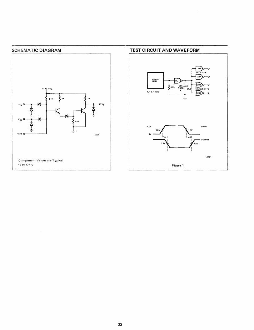
SCHEMATIC DIAGRAM 1--Vee
V 1N I
~ I
"* V IN
t I
* "EXI' 0
Component Values are Typical
*616 Only
4K
t Vo
I ~
1.8K
-=-0252
. ______________________________ -.-J
22
TEST CIRCUIT AND WAVEFORM
~ : Sink F .0.=8
PULSE GEN
t, = It = 15ns
4.0V INPUT
1.5V 1.5V
OV I I I ton I I toftl
I OUTPUT
1.5V 1.5V
I I I I
0252
Figure 1
PIN CONFIGURATION
DUAL 3-INPUT 14 Y.l 12 11 10
SP300A
300 GATE EXPANDER ELECTRICAL CHARACTERISTICS (Notes 1,2,3,5 and 7)
QUAD 2-INPUT 14 13 12 11 10
SP301A/631A
GATE EXPANDERS SP300A Dual 3-lnput
SP301A Quad 2-lnput SP631A Quad 2-lnput
Standard Conditions: V CC = 5.0V, T A = Operating Temp. Range (Unless Noted)
CHARACTERISTIC TEST CONDITIONS MIN. TYP. MAX. UNITS
Expansion Output Voltage Vin == 2.7V, lout = -3.0mA 1.85 V (620n to Gnd.)
Fan-in Expansion of 317 See Text (Page 49) Under 33 NOR Gates
301,631 GATE EXPANDER ELECTRICAL CHARACTERISTICS (Notes 1,2,3,5 and 7) Standard Conditions: V CC = 5.0V, T A = Operating Temp. Range (Unless Noted)
CHARACTERISTIC TEST CONDITIONS MIN. TYP. MAX. UN~TS l
"1" Input Current Vin == 5.0V 10 J.1-A
Diode Forward Voltage I Forward = 2.5mA 0.9 V
Typical Values are for T A == 25°C. See Page 3 for Notes.
SCHEMATIC DIAGRAM SCHEMATIC DIAGRAM
14
IN IN
-, -, -.., -., -, -, -, -, I I I I I I I I
-+. -.t. . ',t; -j; 7s. . .,; .,.- t~~ .. ",. "1· ",. .,. , .~. ·rA
I I I I I I I ~ -:;:- ~ ~ ~ -L -=t: ~
-= 0252 13 12 11 10
Component Values are Typical Component Values are Typical
300A 301A/631A
'-----------.---------------.-~ 23
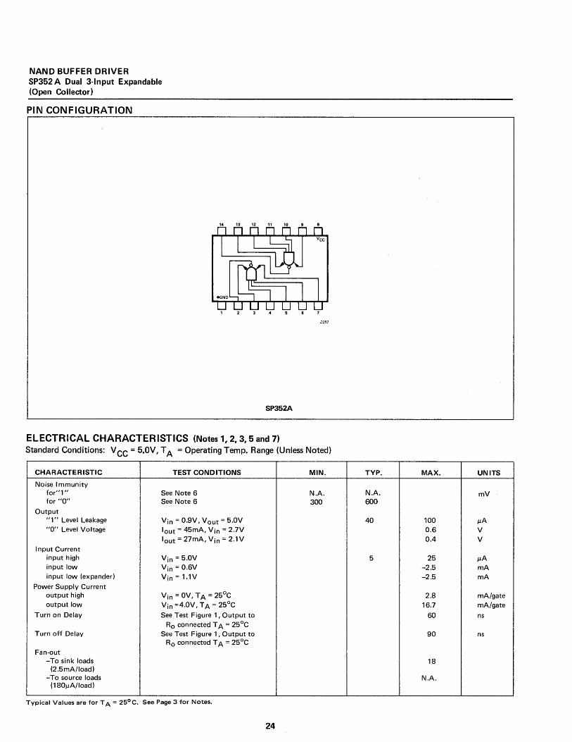
NAND BUFFER DRIVER SP352 A Dual 3-lnput Expandable (Open Collector)
PIN CONFIGURATION
14 13 12 11 10
SP352A
ELECTRICAL CHARACTERISTICS (Notes 1, 2, 3, 5 and 7)
0252
Standard Conditions: V CC = 5.0V, T A = Operating Temp. Range (Unless Noted)
CHARACTERISTIC TEST CONDITIONS MIN.
Noise Immunity for"1 " See Note 6 N.A. for "0" See Note 6 300
Output "1" Level Leakage Vin = 0.9V, Vout = 5.0V "0" Level Voltage lout = 45mA, Vin = 2.7V
lout = 27mA, Vin = 2.1V I nput Current
input high Vin = 5.0V input low Vin = 0.6V input low (expander) Vin=1.1V
Power Supply Current output high Vin = OV, TA = 25°C output low Vin =4.0V, T A = 25°C
Turn on Delay See Test Figure 1, Output to Ro connected T A = 25°C
Turn off Delay See Test Figure 1, Output to Ro connected T A = 25°C
Fan-out -To sink loads
(2.5mA/load) -To source loads
(180j.LA/load)
Typical Values are for T A = 25°C. See Page 3 for Notes.
24
TYP. MAX. UNITS
N.A. mV 600
40 100 }.LA 0.6 V 0.4 V
5 25 }.LA -2.5 mA -2.5 mA
2.8 mA/gate 16.7 mA/gate
60 ns
90 ns
18
N.A.
SCHEMATIC DIAGRAM
VCC
460 UK
VIN I
-.' .,t. I
* I
VIN 'A' a,t. ,i- I
.,t. '*' I
'*' VIN
••• ., .. -I
'*' • EXP
Component values shown are typical
Ro
VOUT
0252
25
TEST CIRCUIT AND WAVEFORM
PULSE GEN
51l!
~ I SINK F.O. = 18
C = I SOURCE F.O. = 5 t, = tf = 15 ns 15pF~
'-----.... ~ 0252
4.0V I I
1.5V 1.5V INPUT I I
OV I I I
-""0:__ -""j:-1.5V\. : 1.5V OUTPUT
I I I I I I
0252
Figure 1
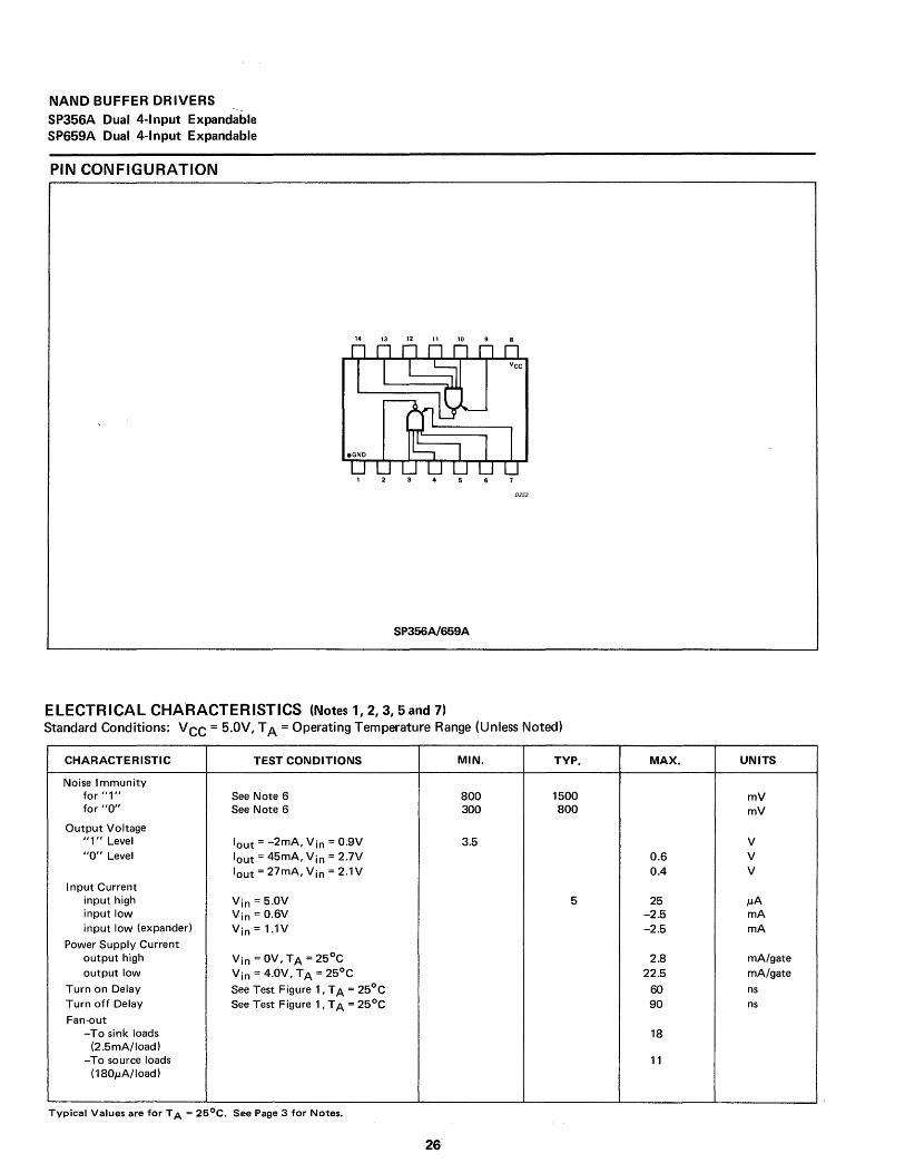
NAND BUFFER DRIVERS SP356A Dual 4-1 nput Expandable SP659A Dual 4-lnput Expandable
PIN CONFIGURATION
14 13 12 11 10
SP356A/659A
ELECTRICAL CHARACTERISTICS (Notes 1,2,3,5 and 7) Standard Conditions: V CC = 5.0V, T A = Operating Temperature Range (Unless Noted)
CHARACTERISTIC TEST CONDITIONS MIN. TYP.
Noise Immunity for "1" See Note 6 800 1500 for "0" See Note 6 300 800
Output Voltage "1" Level lout = -2mA, Vin = 0.9V 3.5 "0" Level lout = 45mA, Vin = 2.7V
lout = 27mA, Vin = 2.1V Input Current
input high Vin = 5.0V 5 input low Vin = 0.6V input low (expander) Vin=1.1V
Power Supply Current output high Vin =OV, TA = 25°C output low Vin = 4.0V, TA = 25°C
Turn on Delay See Test Figure 1 , T A = 25°C Turn off Delay See Test Figure 1, T A = 25°C
Fan-out -To sink loads
(2.5mA/load) -To source loads
(180/JA/load)
Typical Values are for T A = 25°C. See Page 3 for Notes.
26
MAX. UNITS
mV mV
V 0.6 V 0.4 V
25 /JA -2.5 mA -2.5 mA
2.8 mA/gate 22.5 mA/gate
60 ns 90 ns
18
11
SCHEMATIC DIAGRAM
IN 0--..... --«1-.. ,', I,~
I
* IN o--.... --KI-..
IN <r-..... --f(J-..
'." I,~
I
* IN <r-..... --KI-..
' .. I,~
I
* *EXp<r-----~
Component Values are Typical
Vee
1K
t----<t--o OUTPUT
0252
TEST CIRCUIT AND WAVEFORM
PULSE GEN
t,= tf = 15 ns
~ : .SINK F.O. = 17
387
S1n c = I 15PF~=11
'-----..... ~
0252
4.0V 1.5V ~ 1.5Y INPUT
~ ~ -..1 ton 1"'- __ I toft ~
OV 1
1.SV . 1.5V OUTPUT
1 1 1 1
0252
Figure 1
The following curves are normalized, when applicable, to the standard data sheet conditions,
I I I
DRIVER
356
25°C
Vce 5.0V
250
200
",. ,..-
..... V ./V
V
150
100
50
o o 0.2 0.4 0.6 0.8 1.0 1.2 1.4 1.6 1.8 2.0
OUTPUT COLLECTOR VOL TAGE (VOL TSI
27
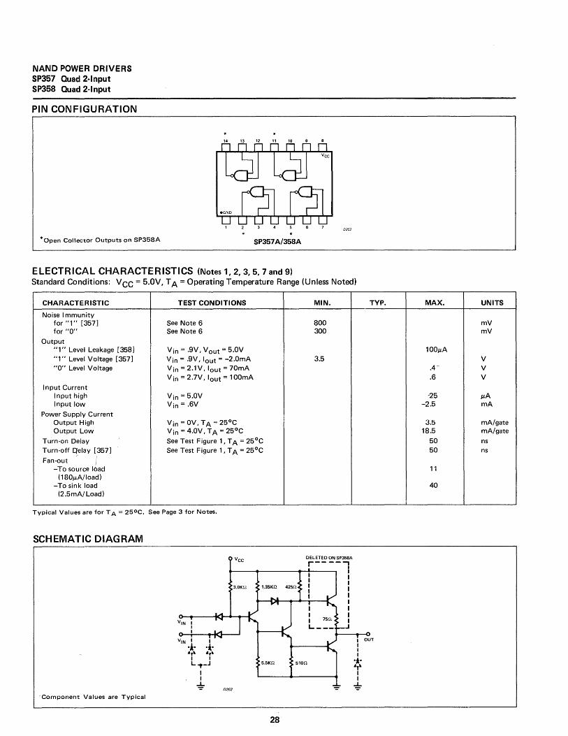
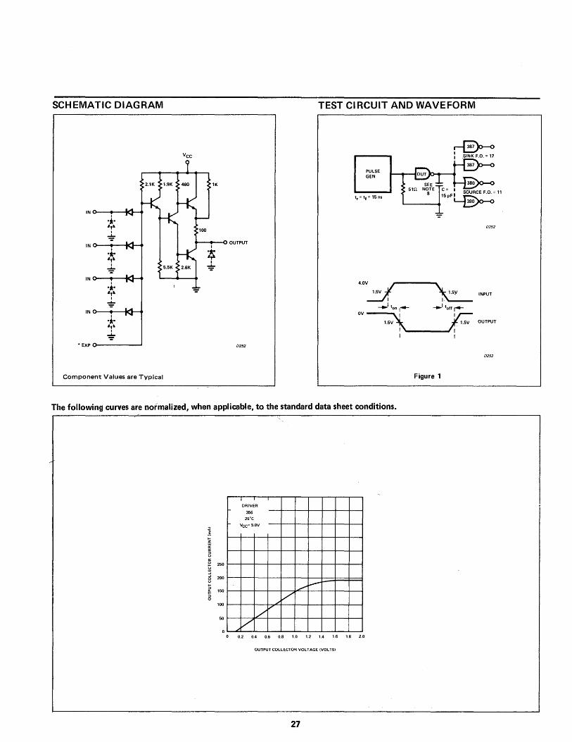
NAND POWER DRIVERS SP357 Quad 2-lnput SP358 Quad 2-lnput
PIN CONFIGURATION
*Open Collector Outputs on SP358A
14 13 12 11 10
SP357 A/358A
ELECTRICAL CHARACTERISTICS (Notes 1,2,3,5,7 and 9) Standard Conditions: VCC = 5.0V, T A = Operating Temperature Range (Unless Noted)
CHARACTERISTIC TEST CONDITIONS
Noise Immunity for "1" [357] See Note 6 for "0" See Note 6
Output "1" Level Leakage [:358] Yin = .9V, Vout = 5.0V "1" Level Voltage [357] Yin = .9V, lout = -2.0rnA "0" Level Voltage Yin = 2.1V, lout = 70rnA
Yin = 2.7V, lout = 100mA Input Current
Input high Yin = 5.0V Input low Yin = .6V
Power Supply Current Output High Yin = OV, T A = 25°C Output Low Yin =4.0V, TA =25OC
Turn-on Delay I See Test Figure 1, T A = 25°C Turn-off qelay [357] See Test Figure 1, T A = 25°C
Fan-out I -To source 16ad
(180p.A/load) -To sink load
(2.5mA/Load)
Typical Values are for T A = 25°C. See Page 3 for Notes.
SCHEMATIC DIAGRAM
'Component Values are Typical
V1N I I I
0252
Vcc
3.0KU
5.5KU
28
MIN.
800 300
3.5
DELETED ON SP358A
510U
r----.., I
I I I I I I I I I I
I I I I
_.J
TYP.
lOUT I I I
"A-',~ I I
~
MAX. UNITS
rnV rnV
100p.A V
.4""" V
.6 V
-25 p.A -2.5 rnA
3.5 rnA/gate 18.5 rnA/gate
50 ns 50 ns
11
40
TEST CIRCUIT AND WAVEFORM
~ SINK F.O. = 40
INPUT
OUTPUT
0252
I I SOURCE F.O. = 11
~
Figure 1
29
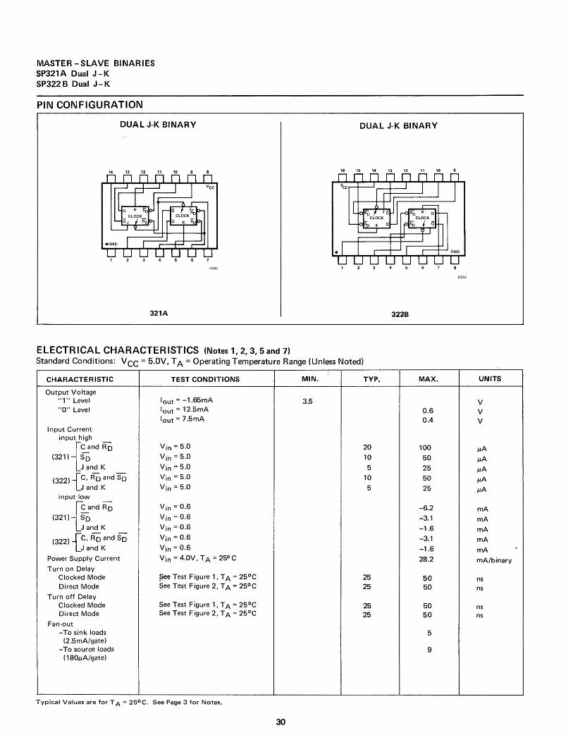
MASTER -SLAVE BINARIES SP321 A Dual J - K SP322 B Dual J - K
PIN CONFIGURATION
DUAL J-K BINARY
14 13 12 11 10
321A
ELECTRICAL CHARACTERISTICS (Notes 1,2,3, 5and 7)
DUAL J-K BINARY
16 15 1. 13 12 11 10
322B
Standard Conditions: VCC = 5.0V, T A = Operating Temperature Range (Unless Noted) I
CHARACTERISTIC TEST CONDITIONS MIN. TYP. MAX.
Output Voltage "1" Level lout = -1.65mA 3.5 "0" Level lout = 12.5mA 0.6
lout = 7.5mA 0.4 Input Current
input high
{Cand RD Vin = 5.0 20 100 (321) So Vin = 5.0 10 50
J and K Vin = 5.0 5 25
(322l{C, RO and So Vin = 5.0 10 50 J and K Vin = 5.0 5 25
input low t -C and RO Vin = 0.6 -6.2 (321) So Vin = 0.6 -3.1
J and K Vin = 0.6 -1.6
(322) {C, RO and So Vin = 0.6 -3.1 J and K Vin = 0.6 -1.6
Power Supply Current Vin = 4.0V, T A = 25°C 28.2 Turn on Oelay
Clocked Mode ~ee Test Figure 1, T A = 25°C 25 50 Oirect Mode See Test Figure 2, T A = 25°C 25 50
Turn off Oelay Clocked Mode See Test Figure 1, T A = 25°C 25 50 Oirect Mode See Test Figure 2, T A = 25°C 25 50
Fan-out -To sink loads 5
(2.5mA/gate) - To source loads 9
(180J.LA/ gate)
Typical Values are for T A = 25°C. See Page 3 for Notes.
30
D252
UNITS
V V V
}.LA
}.LA
}.LA
}.LA
}.LA
rnA
rnA
mA
rnA
rnA
mA/binary
ns ns
ns ns
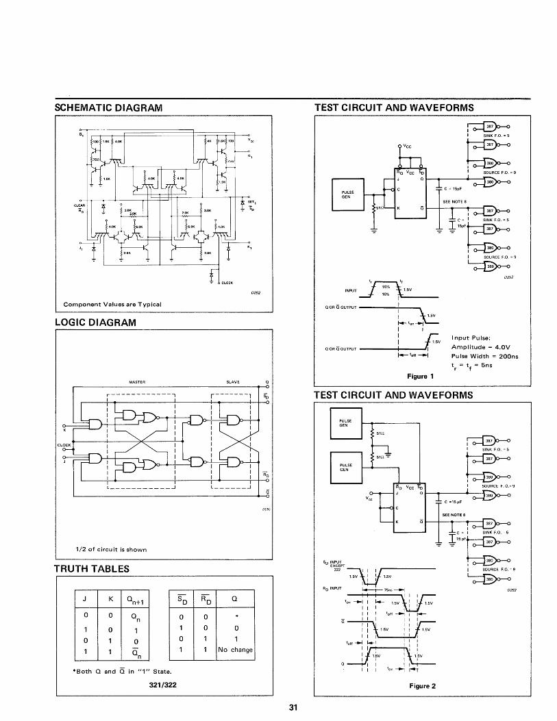
SCHEMATIC DIAGRAM
0252
Component Values are Typical
LOGIC DIAGRAM
MASTER SLAVE Q
r------------.., r-------,
___________ --1 L ______ ...J
1/2 of circu it is shown
TRUTH TABLES
-J K Qn+1 So RO Q
0 0 Qn 0 0 *
1 0 1 1 0 0
0 1 0 0 1 1
1 1 Qn
1 1 No change
* Both Q and Q in "1" State.
321/322
31
TEST CIRCUIT AND WAVEFORMS
PULSE GEN
51!!
SEE NOTE 8
~
~I SI::F.0.=5
380 I I SOURCE F.O. = 9
I
~ l:~'j::: 380
I
INPUT t~f 1.5V
.....J- 10% ~ , Q OR Q OUTPUT ---__ +, __ """
: ~1.5V f.4-ton~~ , I
: Fv Q OR Q OUTPUT ____ --11 ___ ..1.1
f4- toff---J
Figure 1
I SOURCE F.O. = 9
~ 0252
Input Pu Ise:
Amplitude = 4.0V
Pulse Width = 200ns
\ = t f = 5ns
TEST CIRCUIT AND WAVEFORMS
PULSE GEN
PULSE GEN
5H!
51n-=-
AD VCC SO SOURCE F. 0.= 9
J Q~-1------~--~
SEE NOTE 8
Q J---+--+--+--i
SD ~N:~ETpT
322~11 1.5V I I 1.5V
I I I
RD INPUT ~ 75n, ---.-j
I I
ton ~ I I-- 1.5V
I I I I II I toff~ I ~
Q I I I I I I
---:tJJF1 I I I I I 1.5V I I 1.5V
" I I I I toff ~ 14-1 I I I
1 I: : I 1.'5V I 1:5V I I I I
Q I I I I I I I ton ---, j4"j
Figure 2
I
l:';'j;:: 380
I
I SOURCE F.O. = 9
~ 0252
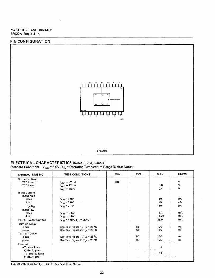
MASTER-SLAVE BINARY SP620A Single J-K
PIN CONFIGURATION
SP620A
ELECTRICAL CHARACTERISTICS (Notes 1,2,3,5 and 7) Standard Conditions: VCC = 5.0V, T A = Operating Temperature Range (Unless Noted)
CHARACTERISTIC TEST CONDITIONS MIN.
Output Voltage "1" Level lout = -2mA 3.8 "0" Level lout = 12mA
lout = 5mA Input Current
input high clock Vin = 5.0V J, K Vin = 5.0V
RD,SD Vin = 2.7V
input low clock Vin = 0.6V J, K Vin = 0.6V
Power Supply Current Vin = 4.0V, TA = 25°C
Turn on Delay clock See Test Figure 1, T A = 25°C preset See Test Figure 2, T A = 25°C
Turn off Delay clock See Test Figure 1, T A = 25°C preset See Test Figure 2, T A = 25°C
Fan-out -To sink loads
(2.5mA/gate) -To source loads
(180J,lA/gate)
Typical Values are for T A = 25°C. See Page 3 for Notes.
32
TYP. MAX. UNITS
V 0.6 V 0.4 V
50 J,lA 25 J,lA
180 J,lA
-1.7 rnA -1.25 rnA
38.0 rnA
55 100 ns 65 150 ns
90 150 ns
95 175 ns
4 ..
)
11 <. . , , - ~
• • <~
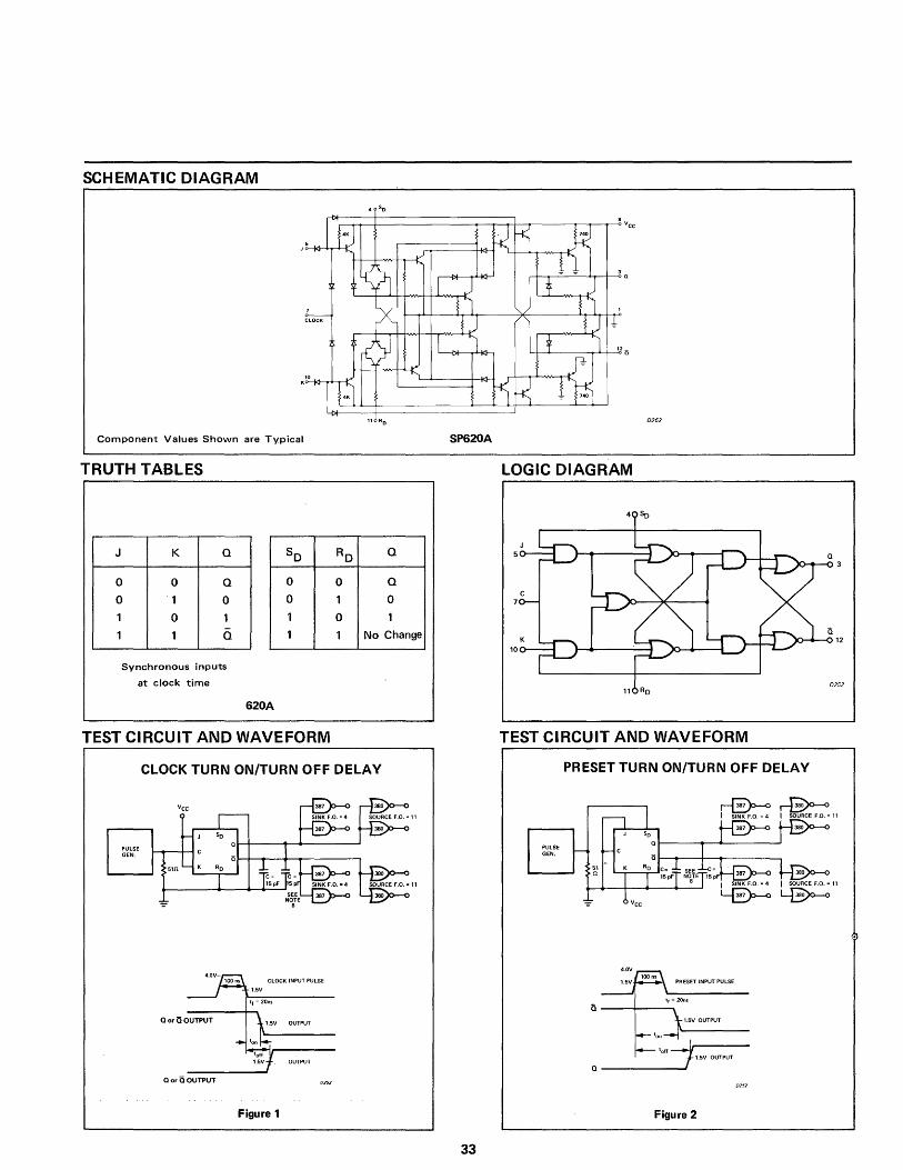
SCHEMATIC DIAGRAM
Component Values Shown are Typical
TRUTH TABLES
J K Q
0 0 Q
0 1 0
1 0 1
1 1 Q
Synchronous inpub
at clock time
So
0
0
1
1
620A
TEST CIRCUIT AND WAVEFORM
RO Q
0 Q
1 0
0 1
1 No Change
CLOCK TURN ON/TURN OFF DELAY
PULSE GEN.
Vcc
5Ul
OUTPUT
OUTPUT
Figure 1
SP620A
33
0252
LOGIC DIAGRAM
TEST CIRCUIT AND WAVEFORM
PRESET TURN ON/TURN OFF DELAY
PULSE GEN.
51 n
a---+--""'\ 1.5V OUTPUT
Q ______ ...J
Figure 2
rG>o---o I SOURCE F.O.· 11
D-TYPE BINARY SP328A Dual
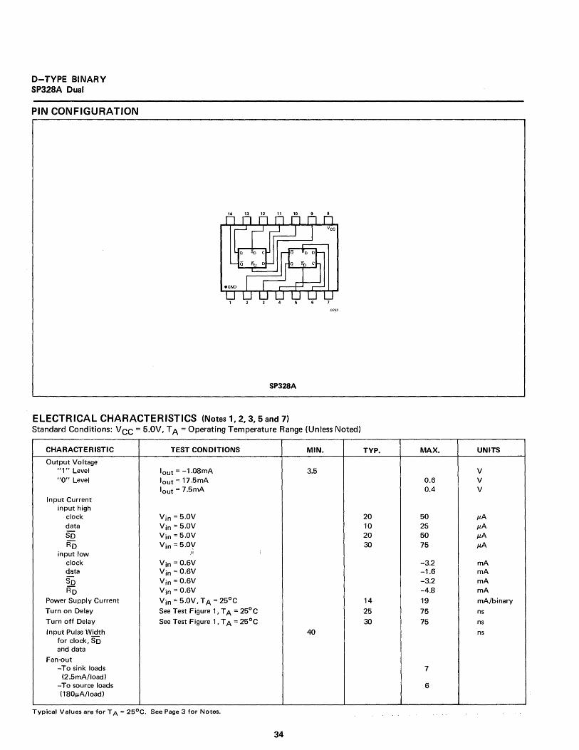
PIN CONFIGURATION
14 13 12 11 10
SP328A
ELECTRICAL CHARACTERISTICS (Notes', 2, 3, 5 and 7)
0252
Standard Conditions: VCC = 5.0V, T A = Operating Temperature Range (Unless Noted)
CHARACTERISTIC TEST CONDITIONS MIN.
Output Voltage "1" Level lout = -1.08rnA 3.5 "0" Level lout = 17 .5 rnA
lout = 7.5rnA Input Current
input high clock Vin = 5.0V data Vin = 5.0V So Vin = 5.0V RO Vin = 5.0"
input low .J'
clock Vin = 0.6V data Vin = 0.6V
So Vin = 0.6V RD Vin = 0.6V
Power Supply Current Vin = 5.0V, T A = 25°C Turn on Oelay See Test Figure 1, T A = 25°C
Turn off Delay See Test Figure 1, T A = 25°C
Input Pulse Width 40 for clock, So and data
Fan-out -To sink loads
(2.5rnA/load) -To source loads (180J.tA/load)
Typical Values are for T A = 25°C. See Page 3 for Notes.
34
TYP. MAX. UNITS
V 0.6 V 0.4 V
20 50 J.tA 10 25 J.tA 20 50 J.tA 30 75 J.tA
-3.2 rnA -1.6 rnA -3.2 rnA -4.8 rnA
14 19 rnA/binary
25 75 ns
30 75 ns
ns
7
6
.SCHEMATIC'DIAGRAM
4K 1.6K 1K
4.12
Clod<
5.11 L4----+----_+___,
Data
6.10
7.9
Component Values are Typical
LOGIC DIAGRAM
SDo-----.------~
Q
CLOCK o--t::t:~:::;::::::IL)
DATA o----+-------t
RDO---~---4---------~ 0252
35
TRUTH TABLES
On Qn+1 On+1
1 1 0 0 0 1
So RO Q
1 1 Q
1 0 0 0 1 1 0 0 t
t Both outputs in 1 state
n is time prior to clock
n+1 is time following clock
TEST CIRCUIT AND WAVEFORM
PULSE GEN.
PULSE GEN.
:0-0 : SINK F.O. = 7
387
C SOURCE F .0. = 6
Q
DUT
Q
D RD
51n
VCC
-=- : SINK F.O. = 7
~
CLOCK PULSE __ -+-.Ij
r- tSETUP 20 ns
----+-1 ""\ r--Q/OOUT:U':~'~~J~ ,Toft
Clock Pulse:
Amplitude = 4.0V, P.W. =
200ns, \ = tf
= 5ns, f = 2 MHz.
D Input:
Amplitude = 4.0V, P.W. = 500n6,
\ = t f = 5ns, f = 1 MHz.
Figure 1
0252
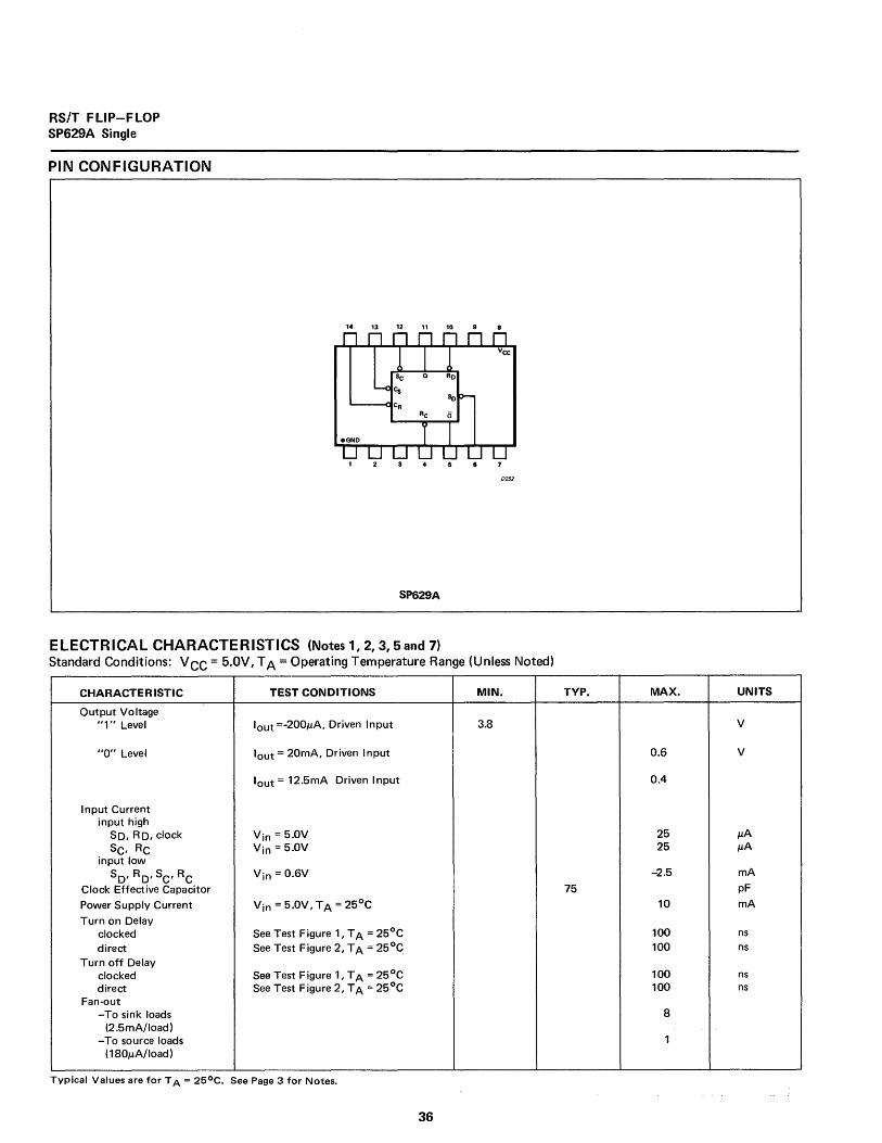
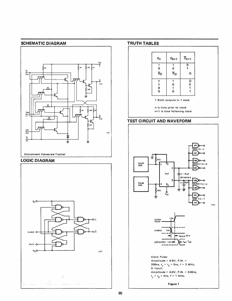
RS/T FLIP-FLOP SP629A Single
PIN CONFIGURATION
14 13 12 11 10
SP629A
ELECTRICAL CHARACTERISTICS (Notes 1, 2, 3, 5 and 7) Standard Conditions: V CC = 5.0V, T A = Operating Temperature Range (Unless Noted)
CHARACTERISTIC TEST CONDITIONS MIN.
Output Voltage "1" Level lout =-200J,tA, Driven Input 3.8
"0" Level lout = 20mA, Driven Input
lout = 12.5rnA Driven Input
Input Current input high
SO, RD, clock Vin = 5.0V SC, RC Vin = 5.0V
input low
SO' RD, SC' RC Vin = 0.6V
Clock Effective Capacitor
Power Supply Current Vin = 5.0V, T A = 25°C
Turn on Delay clocked See Test Figure 1, T A = 25°C direct See Test Figure 2, T A = 25°C
Turn off Delay clocked See Test Figure 1, T A = 25°C direct See Test Figure 2, T A = 25°C
Fan-out -To sink loads
(2.5mA/load) -To source loads
(180J,tA/load)
Typical Values are for T A = 25°C. See Page 3 for Notes.
36
TYP. MAX. UNITS
V
0.6 V
0.4
25 J,tA 25 J,tA
-2.5 rnA
75 pF
10 rnA
100 ns 100 ns
100 ns 100 ns
8
1
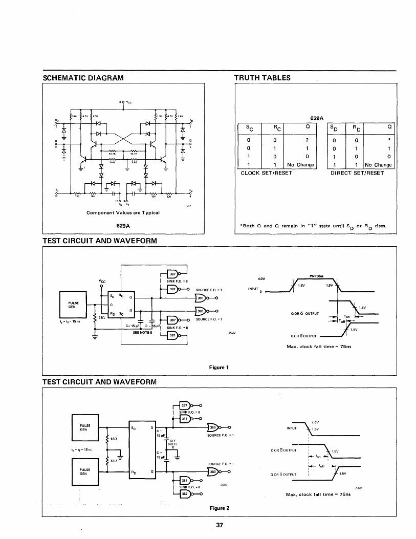
SCHEMATIC DIAGRAM
10 I
1:
~ I
',: -,-~
B Vee
,j,
~
Component Values are Typical
629A
TEST CIRCUIT AND WAVEFORM
TEST CIRCUIT AND WAVEFORM
PULSE GEN t------ISD
511l
51H ':"
c-
SINK F.O. = 8
r-E»--o I SINK F.O. = 8
NOTE 8 nEE
15 pF ':"
PULSE GEN t-..... ---... RD Q~-~~------I
I SINK F.O. = 8
~
TRUTH TABLES
629A
Sc RC Q So RO Q
0 0 ? 0 0 * 0 1 1 0 1 1
1 0 0 1 0 0
1 1 No Change 1 1 No Change
CLOCK SET/RESET 01 RECT SET/RESET
*Both Q and Q remain in "1" state until SD or RD rises.
4.0V
INPUT o
D252
Max. clock fall time = 75ns
Figure 1
~ 4.0V
INPUT ~1.5V
I~--------------I
OOR o OUTPUT : ~ I 15V ~ ton -l "' ____ _ I I I _ toff ----. __ ----
! !1.5V OOR a OUTPUT
0252
Max. clock fall time = 75ns
Figure 2
37
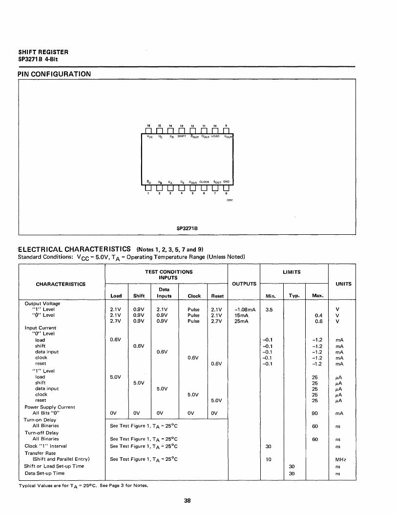
SHIFT REGISTER SP3271 B 4·Bit
PIN CONFIGURATION
16 15 14 13 12 " 10
SP3271B
'ELECTRICAL CHARACTERISTICS (Notes 1,2,3,5,7 and 9)
0252
Standard Conditions: V CC = 5.0V, T A = Operating Temperature Range (Unless Noted)
TEST CONDITIONS INPUTS
CHARACTERISTICS OUTPUTS Data
Load Shift Inputs Clock Reset
Output Voltage "1" Level 2.1V 0.9V 2.1V Pulse 2.1V -1.0BmA "9" Level 2.1V 0.9V 0.9V Pulse 2.1V 15mA
2.7V 0.9V 0.9V Pulse 2.7V 25mA I nput Current
"0" Level load 0.6V shift 0.6V data input 0.6V clock 0.6V reset 0.6V
"1'-' Level load 5.0V shift 5.0V data input 5.0V clock 5.0V reset 5.0V
Power Supply Current All Bits "0" OV OV OV OV OV
Turn-on Delay All Binaries See Test Figure 1, T A = 25°C
Turn-off Delay All Binaries See Test Figure 1, T A = 25°C
Clock "1" Interval See Test Figure 1, T A :::, 25°C
Transfer Rate (Shift and Parallel Entry) See Test Figure 1, T A = 25°C
Shift or Load Set-up Time
Data Set-up Time
Typical Values are for T A = 25°C. See Page 3 for Notes.
38
LIMITS
UNITS
Min. Typ. Max.
3.5 V 0.4 V 0.6 V
-0.1 -1.2 mA -0.1 -1.2 mA -0.1 -1.2 mA -0.1 -1.2 mA -0.1 -1.2 mA
25 pA 25 pA 25 pA 25 pA 25 pA
90 mA
60 ns
60 ns
30 ns
10 MHz
30 ns
30 ns
SCHEMATIC DIAGRAM
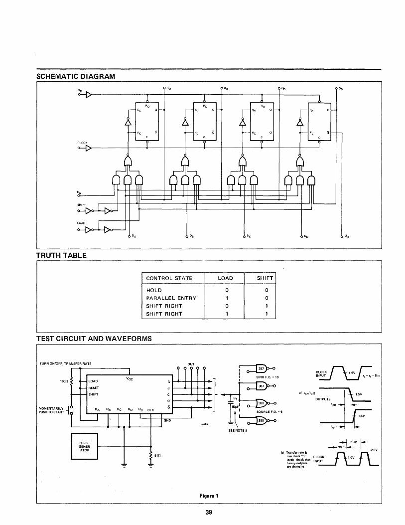
TRUTH TABLE
CONTROL STATE
HOLD
PARALLEL ENTRY
SHIFT RIGHT
SHIFT RIGHT
TEST CIRCUIT AND WAVEFORMS
TURN ON/OFF, TRANSFER RATE
10012
MOMENTARilY J PUSH TO START 1
~ lOAD . ~ RESET --- SHIFT
C DA
I L-J
PULSE GENER· ATOR
DB
I'
OUT
1 r c Vce
A
B
C
0
DC DO Os ClK 6
I I I I I GND
5112
-'- -'-
LOAD SHIFT
0 0
1 0
0 1
1 1
~ I
}
: SINK F.O. = 10
~::: I5tF: SOURCE F.O. = 6
0252
Figure 1
39
-\ ~ SEE NOTE 8
bl Transfer rate & min clock "1" level: check that binary outputs are changing
CLOCK r-\... 1.5V I IN:::..J ~ tr = tf = 5 n,
OUTPUTS
--l 70n, I-----130 n, I-- I
·2.0V
CLOCK ~ 1.0V ~ INP~ '----I L
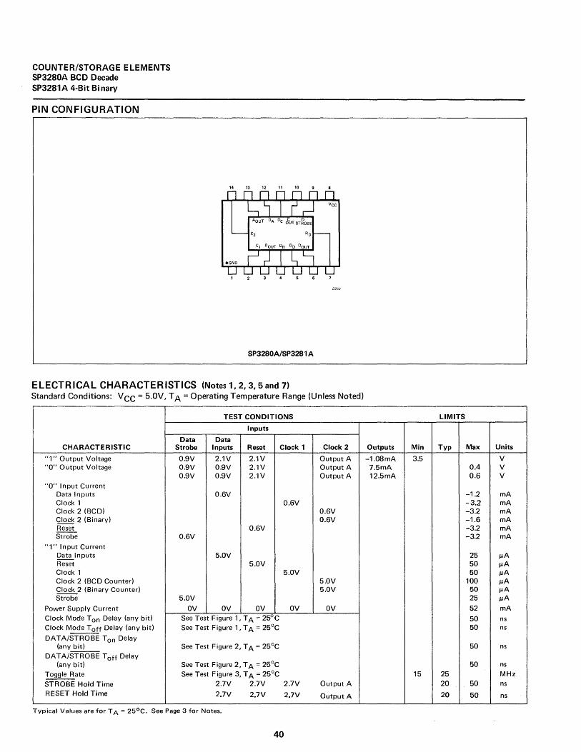
COUNTERfflTORAGEELEMENTS SP3280A BCD Decade SP3281A 4-Bit Binary
PIN CONFIGURATION
14 13 12 11 10
SP3280A/SP3281 A
ELECTRICAL CHARACTERISTICS (Notes 1,2,3,5 and 7) Standard Conditions: VCC = 5.0V, T A = Operating Temperature Range (Unless Noted)
TEST CONDITIONS
Inputs
Data Data CHARACTERISTIC Strobe Inputs Reset Clock 1 Clock 2
"1" Output Voltage 0.9V 2.1V 2.1V Output A "0" Output Voltage 0.9V 0.9V 2.1V Output A
0.9V 0.9V 2.1V Output A
"0" Input Current Data Inputs 0.6V Clock 1 0.6V Clock 2 (BCD) 0.6V Clock 2 (Binary) 0.6V Reset 0.6V Strobe 0.6V
"1" Input Current Data Inputs 5.0V Reset 5.0V Clock 1 5.0V Clock 2 (BCD Counter) 5.0V Clock 2 (Binary Counter) 5.0V Strobe 5.0V
Power Supply Current OV OV OV OV OV Clock Mode Ton Delay (any bit) See Test Figure 1, T A = 25°C Clock Mode T off Delay (any bit) See Test Figure 1, T A = 25°C
DATA/STROBE Ton Delay (any bit) See Test Figure 2, T A = 25°C
DATA/STROBE Toft Delay (any bit) See Test Figure 2, T A = 25°C
Toggle Rate See Test Figure 3, T A = 25°C
STROBE Hold Time 2.7V 2.7V 2.7V Output A
RESET Hold Time 2.7V 2.7V 2.7V Output A
Typical Values are for T A = 25°C. See Page 3 for Notes.
40
LIMITS
Outputs Min Typ Max Units
-1.0BmA 3.5 V 7.5mA 0.4 V 12.5mA 0.6 V
-1.2 mA -3.2 mA -3.2 mA -1.6 mA -3.2 mA -3.2 mA
25 /-LA 50 /-LA 50 /-LA
100 /-LA 50 /-LA 25 /-LA
52 mA
50 ns 50 ns
50 ns
50 ns
15 25 MHz 20 50 ns
20 50 ns
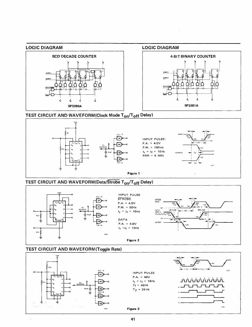
LOGIC DIAGRAM LOGIC DIAGRAM
BCD DECADE COUNTER
SP3280A
TEST CI RCU IT AND WAVE FORM (Clock Mode T on/T off Delay) 5.0V
F 0:: 5
~ I
51H 0 8
I
~
Figure 1 '
INPUT PULSE:
P.A. = 4.0V
P.W. = 100ns
tr = tf = 10 ns
PRR = 5 MHz
TEST CIRCUIT AND WAVE FORM (Data/Strobe Ton/Toff Delay)
5.0V
5Hl
F.O." 5
~ I I
I I
~ F.O. "6
INPUT PULSE
STROBE
P.A. = 4.0V
P.W. = 50ns
tr = tf = 10ns
DATA
P.A. = 4.0V
tr =tf = 10ns
Figure 2
TEST CIRCUIT AND WAVEFORM(Toggle Rate)
'Kll
TO OUTPUTS
F.O." 5
~ I 1
I
~.
INPUT PULSE
P.A. = 4.0V
tr = tf = 10 ns
T1 = 40ns
T2=26ns
Figure 3
41
4-BIT BINARY COUNTER
SP3281A
--1 til-I I
9~o/5V I I ,;'(;" I '0% '0% I I--pw~--ov
--I-I ---i \5V
OUTPUTS ----l ton ~~---
i Y,5V I /I'
-.< toff I.-
1 2 3 4 5 6 7 8 9 10
.I1..IUU'UUU'Ul
A~
8~
'---______________ ~r---L
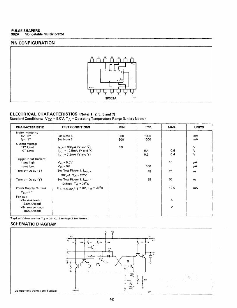
PULSE SHAPERS 362A Monostable Multivibrator
PIN CONFIGURATION
14 13 12 11 10
SP362A
E lECTR ICAl CHARACTER ISTICS (Notes 1,2,3,5 and 7) Standard Conditions: V CC = 5.OV, T A = Operating Temperature Range (Unless Noted)
CHARACTERISTIC TEST CONDITIONS
Noise Immunity for "0" See Note 6 for "1" See Note 6
Output Voltage lout = 360~A (Y and Vi "1" Level
"0" Level lout = 12.5mA (Y and Y) lout = 7.5mA (Y and Y)
Trigger I nput Current input high Yin = 5.0V input low Yin = OV
Turn off Delay (Y) See Test Figure 1, lout =
360~A TA = 25°C
Turn or Delay (y) See Test Figure 1, lout =
12.5mA T A = 25°C
Power Supply Current RX to 5.0V ,RT = OV, T A = 25°C Yout = 1
Fan-out -To sink loads
(2.5mA/load) -To source loads (180~A/load)
Typical Values are for T A = 25 C. See Page 3 for Notes.
SCHEMATIC DIAGRAM
Component Values are Typical GROUND
MIN.
800 800
3.5
Ax Vee
ITI
42
TRIGGER INPUT
TYP.
1000 1200
0.4 0.3
100
45
35
MAX. UNITS
mV mV
V 0.6 V 0.4 V
10 ~A
~A
75 ns
55 ns
19.0 mA
5
2
TEST CIRCUIT AND WAVEFORM
Vcc
~ I I SINK F.O. = 5
RX VCC I
Y o-........ --t Y M~~~~~~~!~~R Y 1---'"
INPUT
~~ pF SOURCE F.O. = 2
-:!-~~\E' 8 ..... -.
0252
Figure 1
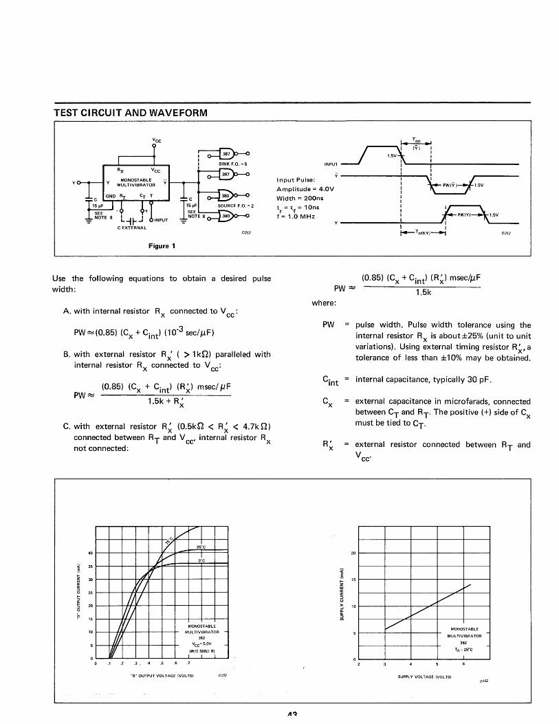
Use the following equations to obtain a desired pulse width:
A. with internal resistor Rx connected to V cc:
B. with external resistor Rx' ( > 1 kO) paralleled with internal resistor Rx connected to V cc:
(0.85) (Cx + Cint) (R~) msecl pF PW~
1.5k + R~
C. with external resistor R~ (0.5kO < R~ < 4.7kO) connected between RT and V cc' internal resistor Rx not connected:
40
/' ~
if 25le
i V oIe
~ r r!;
!J V 11//
l(L MONOSTABLE
MULTIVIBRATOR -
I!J 362
Vee= 5.0V -
VI! (W/O 500n R) I I )
35
30
25
20
15
10
.2 .3..4 .5 .6 .7
"0" OUTPUT VOLTAGE (VOLTS)
Input Pu Ise:
Amplitude = 4.0V
Width = 200ns
\ = tf
= 10ns
f=1.0MHz Y -------!--------f PW(YI=\ ..... '_.5V __ _
PW~
I r--Toff(Y)~
(0.85) (Cx + Cint) (R~) mseclJlF
1.5k
0252
where:
PW
R' x
20
pulse width. Pulse width tolerance using the internal resistor Rx is about ±25% (unit to unit variations). Using external timing resistor R~, a tolerance of less than ±10% may be obtained.
internal capacitance, typically 30 pF.
external capacitance in microfarads, connected between CT and RT. The positive (+) side of Cx must be tied to CT'
external resistor connected between RT and
Vcc'
15
./ V
...... V ~
10
V MONOSTABLE
MULTIVIBRATOR -
362 -TA = 25°e
o I
2
SUPPL Y VOLTAGE (VOLTS) 0252
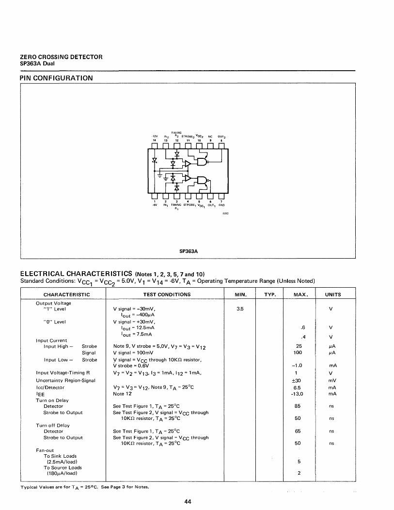
ZERO CROSSING DETECTOR SP363A Dual
PIN CONFIGURATION
TIMING -12V IN2 R2 STROBE2 VCC2 NC OUT2
14 13 12 11 10 9 8
1 -6V
2 3 4 5 8 7 INI TIM~~G STROBEl VCC1 OUT 1 GND
SP363A
ELECTRICAL CHARACTERISTICS (Notes 1,2,3,5,7 and 10) Standard Conditions: VCC, = VCC2 = 5.0V, V, = V'4 = -6V, TA = Operating Temperature Range (Unless Noted)
CHARACTERISTIC TEST CONDITIONS MIN. TYP. MAX.
Output Voltage "1" Level V signal = -30mV, 3.5
'out = -400j.LA
"0" Level V signal = +30mV, lout = 12.5mA .6
'out = 7.5rnA .4 Input Current
Input High - Strobe Note 9, V strobe = 5.0V, V7 = V3 = V12 25 Signal V signal = 100mV 100
Input Low- Strobe '! signal = VCC through 10Kn resistor, V strobe = 0.6V -1.0
Input Voltage-Timing R V7 = V 2 = V 1 3, 13 = 1 rnA, 112 = 1 mA, 1
Uncertainty Region-Signal ±30
I ccl Detector V7 = V3 = V12, Note9, TA = 25°C 6.5 lEE Note 12 -13.0 Turn on Delay
Detector See Test Figure 1, T A = 25°C 85 Strobe to Output See Test Figure 2, V signal = V CC through
10Kn resistor, T A = 25°C 50
Turn off Delay Detector See Test Figure 1, T A = 25°C 65 Strobe to Output See Test Figure 2, V signal = V CC through
10Kn resistor, T A = 25°C 50
Fan-out To Sink Loads
(2.5mA/load) 5 To Source Loads
(180j.LA/load) 2
Typical Values are for T A = 25°C. See Page 3 for Notes.
44
UNITS
V
V
V
j.LA j.LA
mA
V
mV
mA mA
ns
ns
ns
ns
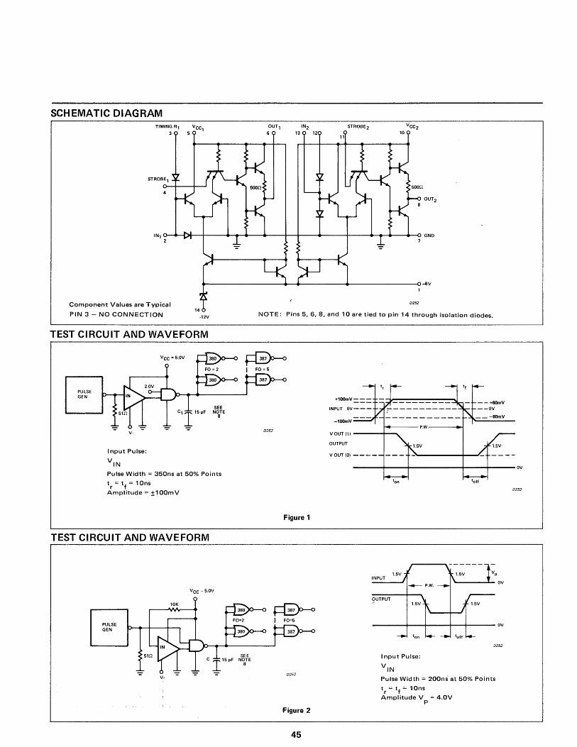
SCHEMATIC DIAGRAM TIMING Rl Vee1
3 5 IN2
13 12 STROBE2
11
STROBEl
INlo-~-C~~~--~~~e---~----~~----e-----~----~-.~~~~~ GND 2
+-------------------~~~--------~~--------------_o~V
Component Values are Typical
PIN 3 - NO CONNECTION ·12V
TEST CIRCUIT AND WAVEFORM
PULSE GEN
V·
Input Pulse:
Vee = 5.0V
SEE NOTE
8
0252
NOTE: Pins 5, 6, 8, and 10 are tied to pin 14 through isolation diodes.
~ I FO = 5
-l00mV ~---- P.W.------..-l
0252 V OUT (1) ---4-... OUTPUT
V OUT (0) - - - -V
IN -----4---4------~--~------OV Pulse Width = 350ns at 50% Points
\ = tf
= 10ns
Amplitude = ±100mV
TEST CIRCUIT AND WAVEFORM
PULSE GEN
Vee =5.0V
SEE NOTE
8
Figure 1
~ I FO=5
0252
Figure 2
45
1.5V INPUT
'------..I.- OV
9UTPUT 1.5V
----4---1------+----+----- OV
0252
I nput Pulse:
VIN
Pulse Width = 200ns at 50% Points
\ = t f = 10ns
Amplitude V p = 4.0V
0252
Section 0) Applications Information ~
HOW TO DESIGN WITH UTILOGIC II
Information in this section gives examples of efficient system design with UTI LOGIC II integrated circuits. The use of the characterization curves presented earl ier for each UTI LOGIC II circuit will be demonstrated here.
Interfacing is discussed, including the interconnecting of UTI LOGIC II and other circuit types. Typical interfacing techniques are illustrated.
Some of the features of UTI LOG IC II that make the family especially interesting to the systems engineer are:
1. High noise immunity, a major design consideration where application may be in high ambient noise environments that are encountered in industrial control equipment, computer peripherals, etc.
2. Low output impedance, essential for good noise immunity, also provides high DC fan-out capabilities. Switching times are relatively unaffected by the increased load capacitance associated with high fan-outs or long inter-connecting lines.
3. Single power supply to provide economy in power supply costs. Tolerance to voltage variations (±10percent) permit the use of simply regulated supplies for further economy.
4. Availability of OR, AND, NOR and NAND logic functions permits straightforward design approaches which means shorter design times and lower package count.
5. Direct interface of UTI LOG IC II to TTL MSI devices ensures that the latest complex functional arrays are available to the designer along with the economy, reliability and simplicity of the UTI LOG IC II logic elements.
All members of the UTI LOGIC II family have built-in protection against damage produced by momentary short circuit conditions, valuable during debugging or troubleshooting procedures. Any input or output connection of any UTI LOGIC II element may be connected to the input, output, supply voltage, or ground connection of any other UTILOGIC II element momentarily, without producing damage to either circuit. It is not recommended that UTI LOGIC II elements be connected so that they produce conditions designated as abnormal for periods of time that can be measured in seconds. If the devices are required to operate for extended periods of time under other than recommended conditions, precautions should be taken to limit the current to safe values within the device's dissipation capabilities.
46
GENERAL DESIGN CONSIDERATIONS
The normal good design practices that are commonly used in layout of networks of any digital circuit family should also be applied to UTI LOGIC II networks. Although all of the UTI LOG IC II elements have excellent noise margins, any circuit, discrete or integrated, will produce erroneous results if the noise levels become high enough. As in any system, ground, DC distribution, and noise problems should be considered from the very beginning of the design.
A major consideration with integrated circuits is the higher packaging density, as compared to discrete devices. For example, a printed circuit board that held 3 or 4 discrete flip-flops can now hold 30 to 40 integrated flip-flops; the design of the DC and ground distribution systems must allow for the corresponding current increases. DC and ground lines should be kept as short as possible and of adequate cross-section, and the use of tantalum or other high-frequency type by-pass capacitors is recommended.
The effect of the high circuit density on system cooling requirements and the increased possibility of localized hot spots must also be considered.
Signal leads should be kept as short as possible to minimize cross-talk, noise pick-up, and propagation time down the wire.
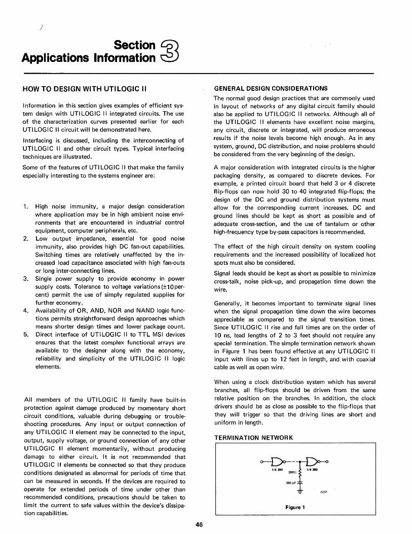
Generally, it becomes important to terminate signal lines when the signal propagation time down the wire becomes appreciable as compared to the signal transition times. Since UTI LOG IC II rise and fall times are on the order of 10 ns, lead lengths of 2 to 3 feet should not require any special termination. The simple termination network shown in Figure 1 has been found effective at any UTI LOGIC II input with lines up to 12 feet in length, and with coaxial cable as well as open wire.
When using a clock distribution system which has several branches, all fl ip-flops should be driven from the same relative position on the branches. In addition, the clock drivers should be as close as possible to the flip-flops that they will trigger so that the driving lines are short and uniform in length.
TERMINATION NETWORK
o----Do---~ 1/4380 1/4380. 300n
300PFI . -= 0252
Figure 1
UTILOGIC II CIRCUITS
UTI LOGIC II inputs are classified as sink loads and source loads by the direction of current flow required to activate the input. The input of the OR and NOR gates are called source loads because they must be driven by a source of current, e.g., the output of a UTI LOG IC II element in the "1" state or a connection to the positive supply. The inputs of the AND gates, NAND gates and the Binary are called sink loads because they must be driven from a current sink: for example, the output of a UTILOGIC II element in the "0" state or a connection to ground.
In this publication, and all other UTI LOGIC II literature, the convention of positive logic, i.e., the positive level is 1/1", has been assumed. If the negative logic notation is assumed (most negative level is "1"), the AND, OR, NAND and NOR gates become OR, AND, NOR and NAND respectively.
The characteristic curves presented in the various sections are designed to allow the system designer to predict system performance characteristics for various operating conditions. In general, characteristics are normalized to the conditions of the specification sheets. The use of the normalized characteristic is a definite design aid in that it is usually the change in the characteristic as a result of a change in the parameter that is of interest.
As long as the effects, e.g.,
aVsat aTemp'
are small, the total effect may be predicted by taking the product of the individual effects.
Throughout the discussion that follows, V cc is assumed to be 5.0V unless otherwtse specified.
UTI LOGIC II NOR Gates and Expander
The UTI LOG IC II NOR gates (314,370, and 380), Expandable NOR gate (317) and Expander (300), are all derived from the same basic circuit to ensure full compatibility of the Expandable Gates and Expander, and to give all the circuits identical electrical characteristics. However, the 300 and 317 will have longer turn-off delay times (T 2) because of the additional capacitive loading on the expansion input. Turn-on delays (T1) are not sensitive to this capacitance because the source impedance is low during turn-on.
The 300 Expander circuit is characterized in terms of its operation in conjunction 'With the 317 Expandable NOR and 333 Expandable OR. The ways in which 300 and 317
47
(as well as 300 and 333) compatibility is guaranteed are of interest. The expansion forward voltage for the 300 and the expansion input voltage of the 317 are measured under the same conditions, and the same limits are guaranteed. In addition, the 300 input leakage current and the 317 "0" input current specifications guarantee reverse current compatibility. These specifications assure the user that the 300 and 317 or the 300 and 333 combination will have the same DC characteristics as when the 317 or 333 is used alone. AC characteristics are shown later (with the 317 and 333 curves) as a function of the capacitance on the expansion input.
CIRCUIT DESCRIPTION
The UTI LOG IC II NOR gate (page 4) may be considered as a derivation of the DTL NOR gate. The input diodes of the DTL NOR were replaced with transistors to decrease the input current to allow larger source fan-out capabilities from the NOR and other circuits in the family. The NOR employs a totem-pole output to obtain low output impedance in both the "1" and "0" states. The switching thresholds are determined by the ratio of the coupling resistance to the pull-down resistance at the base of each switching transistor. The series resistor at the output provides current-limiting should the output become accidentally shorted to ground. The Expandable NOR is implemented by connecting the common emitters of the input transistors to an expansion input. The Expander (page 23) is a dual array of input transistors; thus, the effect of connecting the Expander output to an expansion input is the same as connecting more input transistors in parallel.
Input Characteristics
The Standard UTI LOGIC II Source Load is the NOR input. The Standard Source Load may be simulated by a 15 kn resistor and 2 series silicon diodes to ground. An unused NOR input should be tied to ground through a resistance of 60 kn. (or less) or connected In common with a used input on the same circuit. The capacitance of an open input may become charged during prolonged "1" levels at a driven input. When the driven input goes from "1" to "0", the charged capacitance discharges into the input and gives the effect of a slow circuit. Two or more common inputs represent the same DC load as a single input since the "1" input current is determined by the voltage across the coupling resistors and the gain of the input transistors. Neither of these values changes appreciably when inputs are connected in common. The additional capacitance of a commoned input has no measurable effect on switching times. Input voltages should not exceed the supply voltage unless precautions are taken to limit the resulting current to 30mA in the input transistor collector-base junction.
Output Characteristics
A UTI LOGIC II NOR gate has a fan-out of 5 sink loads and 11 source loads. All 16 loads may be connected simu 1-taneously because they do not interact. Because the NOR gates employ transistors for both pull-up and pull-down, their outputs cannot be connected with the output of any other independent circuit (collector-logic). Such operation of an active pull-up device with another device may result in ambiguous output voltages and/or excessively high currents if one device should attempt to reach a "1" level while the other is attempting to reach a level "0". However, two NORs may be connected with common inputs and common outputs. In this case, fan-out is doubled and the input loading is two Standard Source Loads.
UTI LOG IC II OR Gates
The UTI LOGIC II OR gates are compatible on a pin for pin basis with their UTI LOGIC II NOR gate counterparts. This simplifies system design, circuit board layout and checkout.
Comparison of the schematics of the UTI LOGIC II OR gate (page 8 through 10) and the UTI LOGIC II NOR gate (page 4) shows that both types of gates have essentially identical input and output structures; however, the OR gate uses one more transistor to obtain the additional inversion required to produce an OR gate from the basic UTI LOG IC II NOR configuration.
UTI LOG IC II AND Gates
The UT I LOG I C II AN D gates 305 and 306 are fabricated from the same basic chip, and therefore have identical electrical characteristics. The internal connection pattern is varied to produce a single 6-input AND gate in the 305, and the dual 3-input AN D gates in the 306.
CIRCUIT DESCRIPTION
Schematic diagrams of the UTI LOG I C II AN D gates are shown on page 13. The multiple-emitter input structure provides the same function as a Diode AND gate. The output-emitter follower provides the current gain necessary for high fan-out, and also reduces the offset voltage associated· with Diode AND gates. The emitter follower provides a low output impedance to effect fast response on "0" to "1" transistionsand the current gain necessary for source current fan-out. The input transistor and connecting diode provide a low impedance circuit to maintain good response on "1" to "0" transitions.
48
Input Characteristics
The input of the AND is defined as a standard UTI LOGIC II sink load. The standard sink load may be simulated by 2 k n resistor with a series silicon diode to the supply voltage. The input impedance of UTI LOGIC II AND gates is low enough so that unused inputs may be left open without degrading circuit performance (open inputs are logical "1") however; it is recommended that unused inputs be connected to the used inputs of the circuit. Connecting the unused inputs to used inputs of the same circuit will not increase the circuit loading. The effect of the added capacitance will be negligible.
Output Characteristics
The fan-out of the UTILOGIC II AND gate is 10 to standard UTILOGIC II source loads. The AND gate does not have output current sinking capability; therefore, it cannot drive sink loads. The AND gate can drive any of the UTI LOG I C II source loads. The AN D gate outputs should not be paralleled with the outputs of any other circu its as in collector logic configurations. However, outputs of AND gates may be connected to increase fan-out if the inputs of the two circuits are in common.
UTI LOGIC II NAND Gates and Expander
The UTI LOG IC II NAND gates (337, 377 and 387) and diode expander (301) are DTL gates. This is due to the fact that the basic UTI LOGIC input structure does not lend itself to implementing the NAND function. The NAND gates are compatible with all other elements in the UTI LOGIC II line. In addition, the NAND gates provide a guaranteed interface with Signetics TTL logic elements.
The 301 expander is specified under the same conditions as the gate inputs, thus ensuring that an expanded 337 will have the same input characteristics as the other NAND gates. The 301 may also be used as an expander for the 356 driver element.
CIRCUIT DESCRIPTION
The UTILOGIC II NAND gates (page 17) are modifications of the proven Signetics 600 series circu its. The major change is that the usual 4 k n output resistor has been replaced with a 1 kn resistor. The use of a passive pull-up permits outputs to be connected in parallel to perform collector logic. Input and output levels are fully compatible with the other UTI LOGIC elements and provide a minimum of 800 mV of noise margin in both the "0" and "1" states.
Input Characteristics
The input structure of the NAND gates makes them sink loads. The NAND inputs, like the UTI lOGIC " AND inputs, require that the driving gate to be able to sink 2.5 mA for each such load driven. The UTI lOGIC OR and NOR gates can therefore drive up to 5 NAND gate inputs. As with the AND gates, the input load of the NAND gates may be. simulated by a 2 kn resistor in series with a silicon diode to the supply voltage.
Unused inputs may be left open, however, a more conservative design practice suggests connecting the unused inputs to a driven input. In cases where the source load on the driving gate will not permit connecting the unused inputs to a driven input, the unused inputs may be returned to V cc'
The UTI lOGIC" NAND gates have two sets of input and output specifications to enable the NAN D gates to be used with both UTI lOGIC elements and Signetics TTL logic elements. The "1" level input threshold is specified at 2.7 volts for use with UTI lOGIC driving elements and 2.1 volts for use with TTL driving elements. This is accomplished by reducing the fan-out at the lower input voltage. The "0" level input current in both cases is within the 2.5 mA maximum.
Output Characteristics
A UTI lOG I C " NAN D gate has a fan-out of 12 loads and 6 source loads. All 18 loads may be connected simultaneously. The passive 1 k n pull-up resistor used in the NAND output structure permits collector logic to be performed by connecting the outputs of up to 5 NAND gates in parallel. The resulting "wired AND" gate can drive one sink load and 6 source loads.
In cases where additional fan-out may be required, NAND gates may be connected in parallel. The fan-out can be doubled by connecting two gates in parallel; however, the input loading is also doubled.
The UTI lOGIC II NAND gates can be used to drive Signetics TTL logic elements and complex arrays. When used in conjunction with TTL circuits, the NAND gate sink fan-out is reduced to 12.5 mA at a "0" output voltage of 0.4 volts. In most cases, this will result in a fan-out of 7 to Signetics DCl sink type loads. Refer to the Signetics DCl Handbook for further information on DCl input requ irements.
The 600 Series NAND gates, as stated previously, are the same as the UTI lOGIC NANDS except for the pull-Up resistor which is 4 kn instead of the 1 k n used in UT I lOG I C. Therefore the comments for UT I lOG I C NAND* are applicable to 600 series NANDS with this one difference.
49
Series 600 Inverter
The 690 Inverter has been designed using the same circuit as the 600 NAND gates and provides six inverters in each package.
The circuit description, input and output characteristics are therefore the same as those for the SP600 NAN D gates.
UTILOGIC II Buffer Driver
The UTI lOGIC" 356 Buffer Driver is shown on page 26. It is intended for driving the clock and RESET I ines of the 321 and 322 J-K binaries. The "1" level output impedance of the driver is approximately 150 ohms for output voltages less than one diode drop below V cc' It should also be noted that the use of active outputs for both the "1" and "0" states means that the output of these drivers cannot be connected in parallel with any other element. However, for those cases where high fan-out is required, but absolutely no clock skew can be allowed, two line drivers may be tied in parallel if the inputs also are made common.
The 352 is an open collector variation of the 356. The open collector allows collector logic to be performed in conjunction with the driving capabilities for clock and reset lines.
UTI LOG IC II J-K Binaries
The UTI lOGIC II 321 and 322 are dual J-K general purpose binaries with both synchronous and asynchronous inputs. They employ DC level triggering with clocking effected on the negative-going edge of the clock pulse waveform.
CIRCUIT OPERATION
The 321 and 322 have the following output sequence: 1. With clock pulse low, the logical inputs are disabled
and the slave is connected to the master. 2. At the rise of the clock pulse the slave is disconnected
from the master and the logical inputs are enabled. Data now enters the master, setting it to the state determined by the logical inputs. The information present at the J and K lines prior to or coincident with the rise of the clock, sets the master F F when the clock reaches a logical "1" level. For reliable operation the original J and K inputs must remain stable during the entire clock "1" interval.
3. At the fall of the clock pulse the logical inputs are disabled to prevent entry of further information and the slave is connected to the master. The slave now takes the state of the master and state of the slave appears at the outputs. The J and K inputs of the 321 and 322 are non-inverting, that is, the flip-flop will be set at "1" when the J input is high and the K input is low. The asynchronous inputs are inverting, that is, actu ated by log ical "0". The effect of the asynchronous inputs is independent of the state of the clock line.
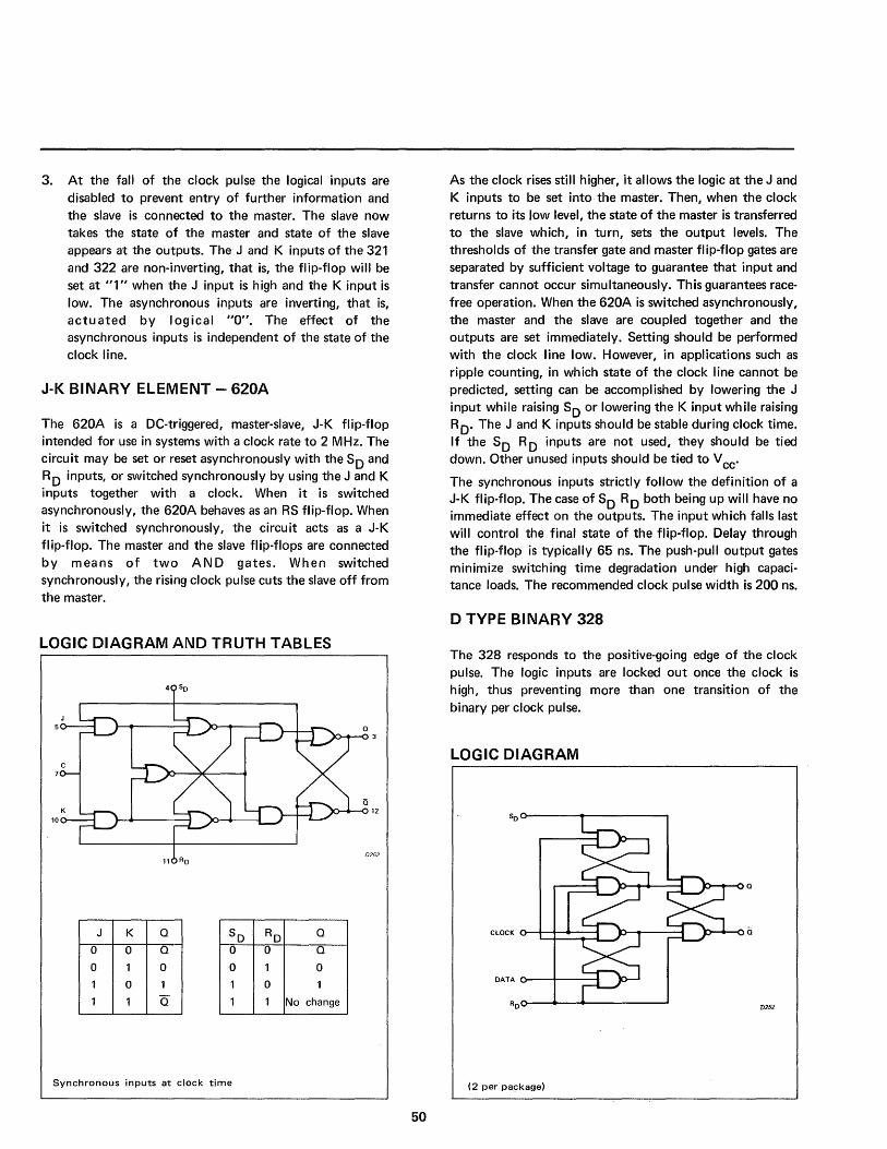
J-K BINARY ELEMENT - 620A
The 620A is a DC-triggered, master-slave, J-K flip-flop intended for use in systems with a clock rate to 2 MHz. The circuit may be set or reset asynchronously with the SD and RD inputs, or switched synchronously by using the J and K inputs together with a clock. When it is switched asynchronously, the 620A behaves as an RS flip-flop. When it is switched synchronously, the circuit acts as a J-K flip-flop. The master and the slave flip-flops are connected by means of two AND gates. When switched synchronously, the rising clock pulse cuts the slave off from the master.
LOGIC DIAGRAM AND TRUTH TABLES
J K Q SD RD Q
0 0 Q 0 0 Q
0 1 0 0 1 0
1 0 1 1 0 1
1 1 Q 1 1 No change
Synchronous inputs at clock time
50
As the clock rises still higher, it allows the logic at the J and K inputs to be set into the master. Then, when the clock returns to its low level, the state of the master is transferred to the slave which, in turn, sets the output levels. The thresholds of the transfer gate and master flip-flop gates are separated by sufficient voltage to guarantee that input and transfer cannot occur simultaneously. This guarantees racefree operation. When the 620A is switched asynchronously, the master and the slave are coupled together and the outputs are set immediately. Setting should be performed with the clock line low. However, in applications such as ripple counting, in which state of the clock line cannot be predicted, setting can be accomplished by lowering the J input while raising SD or lowering the K input while raising RD' The J and K inputs should be stable during clock time. If the SD R D inputs are not used, they should be tied down. Other unused inputs should be tied to V cc'
The synchronous inputs strictly follow the definition of a J-K flip-flop. The case of SD RD both being up will have no immediate effect on the outputs. The input which falls last will control the final state of the flip-flop. Delay through the flip-flop is typically 65 ns. The push-pull output gates minimize switching time degradation under high capacitance loads. The recommended clock pulse width is 200 ns.
D TYPE BINARY 328
The 328 responds to the positive-going edge of the clock pulse. The logic inputs are locked out once the clock is high, thus preventing more than one transition of the binary per clock pulse.
LOGIC DIAGRAM
SDo------4~--------~
Q
CLOCK O-+-+-~---I
DATA 0---+-----1
RDo------~~--------~ 0252
(2 per package)
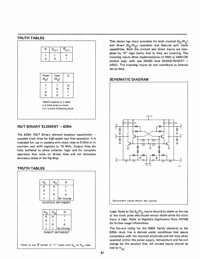
TRUTH TABLES
0 Q n+1 Q n+1
1 1 0 0 0 1
Preset Clear Q
(SO) (RO)
1 1 Q
1 0 0 0 1 1 0 0 +
+Both outputs in 1 state n is time prior to clock n+1 is time following clock
RS/T BINARY ELEMENT - 629A
The 629A RSIT Binary element employs capacitively -coupled clock lines for high-speed race free operation. It is intended for use in systems with clock rates to 5 MHz or in counters and shift registers to 10 MHz. Output lines are fully buffered to allow collector logic and for complete assurance that noise on driven lines will not introduce erroneous states in the fl ip-flop.
TRUTH TABLES
Sc RC Q
0 0 ?
0 1 1
1 0 0
1 1 No Change
CLOCKED SET/RESET
So RO Q
0 0 * 0 1 1
1 0 0
1 1 No Change
01 RECT SET/RESET
* Both Q and Q remain in "1" state until So or RO rises.
51
This device has input provision for both clocked (SciRe) and direct (SD/RD) operation and features split clock capabilities. Both the clocked and direct inputs are energized by "0" logic levels; that is, they are inverting. The inverting inputs allow implementation of AND or AND-OR control logic with one NAND level (NAND-INVERT =
AND). The inverting inputs do not contribute to internal set-up time.
SCHEMATIC DIAGRAM
8 Vee
3.8K 4.2K 1.5K 1.5K 4.2K 3.8K
11 I I 5 .". ',-~
. .. l
Component values shown are typical
Logic levels to the SciRe inputs should be stable at the rise of the clock pulse and should remain stable while the clock input is high. Refer to Signetics Application Note AN108 for further usage information.
The fan-out rating for the 600A family elements to the 629A clock line is derived under conditions that assure compliance with the required amplitude and fall time when operated within the power supply, temperature and fan-out ratings for the product line. All unused inputs should be
tied to V cc'
362 Multivibrator
The 362 is a one-shot multivibrator with complementary outputs and optional 500-ohm load resistors. The output pulse width can be conveniently adjusted to conform to most one-shot application requirements. The 362 provides high output duty cycle (75%) and complete isolation of the timing stage and the output stage, resulting in good fall time even with wide pulse width. The input pulse width should be at least 50 nanoseconds wide, with a fall time of less than 75 nanoseconds, or 1 volt per 25 ns.
The 362 provides complementary outputs with passive 3k ... ohm pull-up resistors. An optional 500 ohm pull-up resistor
is provided at each output, to be used when driving heavy capacitance loads where rise times must be maintained.
The 362 design employs a 30 pF timing capacitor and an optional 1.5k ohm timing resistor. The output pulse width may be varied by appropriate connection of external Rand C at the Ct ' Rt , Ry and Ry terminals.
363 DUAL ZERO CROSSING DETECTOR
The 363 Dual Zero Crossing Detector is a circuit incorporating a differential input and logic gate output. The input ampl ifier is referenced to zero volts and employs temperature compensation to ensure stable thresholds.
INTERFACING CONSIDERATIONS
GENERAL CONSIDERATIONS
The need to interface UTI LOGIC II integrated circuits with discrete component circuitry or with integrated circuits of another family may arise when a UTI LOGIC II system or subsystem is added to or must operate with existing hardware. General rules when interfacing are: 1. Inputs to UTI LOGIC II source loads must be capable
of supplying 1BOJLA input current at the 1t1" input threshold voltage of at least 2.7 volts.
2. Inputs to sink loads must be capable of sinking 2.5 rnA at the "0" voltage (0.6V).
3. A UTI LOG IC II output will supply 2 mA at 3.B volts for NOR and OR gates; it will supply 1.6 mA at 3.B volts for binaries; and 1.B rnA at 3.B volts for ANDs.
4. The approximate equivalent circuit for any UTI LOG IC II output at 1t1" is 100 ohms to 4.0 volts. A NOR, OR and binary output will sink 12.5 mA at 0.6 volts or less.
5. The rise and fall times of signals entering a UTI LOG I C system should be kept to less than 1 JLsec to ensure stable operation and avoid oscillation of the gate driving transition of the threshold.
52
UTI LOGIC II AND DTL
A UTILOGIC II-to-Signetics 100 series DTL (DTL in general) interface requires, at most, modification of load definitions. The input resistor of the DTL NAND gate and the UTI LOGIC II AND are approximately the same value so that the DTL load is equal to a UTILOGIC II sink load. The 1t1" and ItO" levels at UTI LOGIC II outputs are fully compatible with DTL input requ irements and vice versa.
SP600 series DTL elements that have passive pull-up outputs generally have fan-outs of 2 to UTI LOG I C II source loads. Higher source load fan-out can be obtained by providing Bkn of pull-up resistance for each additional source fan-out required. A UTI LOGIC II AND gate may be used as buffer for DTL to UTILOGIC II.
Mixed UTI LOGIC II - DTL systems should operate with a 5.0 volt power supply; the rules above assume a common power supply.
UTI LOGIC II AND TTL
Uti logic 11/600 Series circuits are designed to interface directly with Signetics TTL integrated circuits. The inputs of the TTL devices (BOOO Series or 54/7400 Series) are multiples of 1.6mA with an input voltage of O.4V. The sink current capabiltiy of the Uti logic II and 600 Series devices is specified at VSAT = O.4V and 0.6V in order that fan-out can be calculated for either TTL or Uti logic loads respectively. Since the output voltage of all Uti logic II and 600 Series circuits with either active or passive internal pull-ups is guaranteed to be a minimum of 3.5V, these devices will provide at least 1.5V of "1" level noise margin when driving TTL loads.
For TTL driving Uti logic II or 600 Series circuits, the maximum "0" level output voltage of O.4V will provide up to 800mV of guaranteed noise margin. For most Uti logic 11/ 600 Series circuits, the input threshold voltage is specified at either 2.1 V or 2.7V with corresponding differences in current sink capability. The lower figure of 2.1 V should be used when interfacing directly with TTL outputs. The guaranteed "1" level for the 54/7400 Series is 2.4V providing 300m V of noise margin, while the "1" level output for Signetics BOOO Series circuits is 2.6V minimum which results in 500mV of worst case noise margin.
When driving Utilogic II OR and NOR gates with an input threshold of 2.7V minimum a resistor should be connected between the TTL output and VCC. The resistor value should be chosen such that it maintains a 1/1" level output voltage greater than 2.7V while supplying 1/1" level current to drive the load. The resistor must be large enough so that it does not require excessive I/O" level current sinking capability for the TTL output structure.
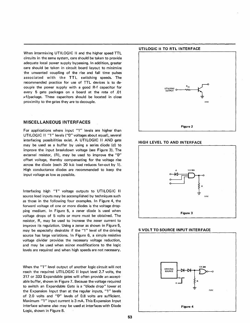
When intermixing UTILOGIC II and the higher speed TTL circuits in the same system, care should be taken to provide adequate local power supply bypassing. In addition, greater care should be taken in circuit board layout to minimize the unwanted coupling of the rise and fall time pulses associated with the TTL switching speeds. The recommended practice for use of TTL devices is to decouple the power supply with a good R-f capacitor for every 5 gate packages on a board at the rate of .01 .uf/package. These capacitors should be located in close proximity to the gates they are to decouple.
MISCELLANEOUS INTERFACES
For applications where input "1" levels are higher than UTI LOGIC II "1" levels ("0" voltages about equal), several interfacing possibilities exist. A UTI LOGIC II AND gate may be used as a buffer by using a series diode (d) to improve the input breakdown voltage (see Figure 3). The external resistor, (R), may be used to improve the "0" offset voltage, thereby compensating for the voltage rise across the diode (each 20 kn load reduces fan-out by 1). High conductance diodes are recommended to keep the input voltage as low as possible.
Interfacing high "1" voltage outputs to UTI LOG IC II source load inputs may be accomplished by techniques such as those in the following four examples. In Figure 4, the forward voltage of one or more diodes is the voltage dropping medium. In Figure 5, a zener diode is used when voltage drops of 5 volts or more must be obtained. The resistor, R, may be used to increase the zener current to improve its regulation. Using a zener as shown in Figure 5, may be especially desirable if the "1" level of the driving source has large variations. In Figure 6, a simple resistive voltage divider provides the necessary voltage reduction, and may be used when minor modifications to the logic levels are required and when high speeds are not necessary.
When the "1" level output of another logic circuit will not reach the required UTILOGIC II input level 2.7 volts, the 317 or 333 Expandable gates will often provide an acceptable buffer, shown in Figure 7. Because the voltage required to switch an Expandable Gate is a "diode drop" lower at the Expansion I nput than at the regular inputs, "1" levels of 2.0 volts and "0" levels of 0.8 volts are sufficient. Maximum "1" input current is 3 mAo This Expansion Input interface scheme also may be used at interfaces with Diode Logic, shown in Figure 8.
53
UTI LOGIC II TO RTL INTERFACE
UTI LOGIC OUTPUT ~
IN
0252
Figure 2
HIGH LEVEL TO AND INTERFACE
1/2306
0252
Figure 3
5 VOLT TO SOURCE INPUT INTERFACE
DRIVING SOURCE
Figure 4
R
1/4380
0252
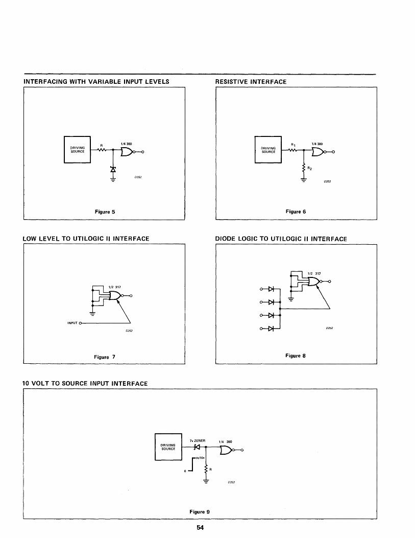
INTERFACING WITH VARIABLE INPUT LEVELS
DRIVING SOURCE
Figure 5
1/4380
0252
LOW LEVEL TO UTI LOGIC II INTERFACE
INPUT 0----------"
0252
Figure 7
10 VOLT TO SOURCE INPUT INTERFACE
DRIVING SOURCE
7v ZENER
r~ .......
, J~'" ~
Figure 9
54
RESISTIVE INTERFACE
R1 1/4380 DRIVING SOURCE
R2
-== 0252
Figure 6
DIODE LOGIC TO UTILOGIC II INTERFACE
0252
Figure 8
1/4 380
R
0252
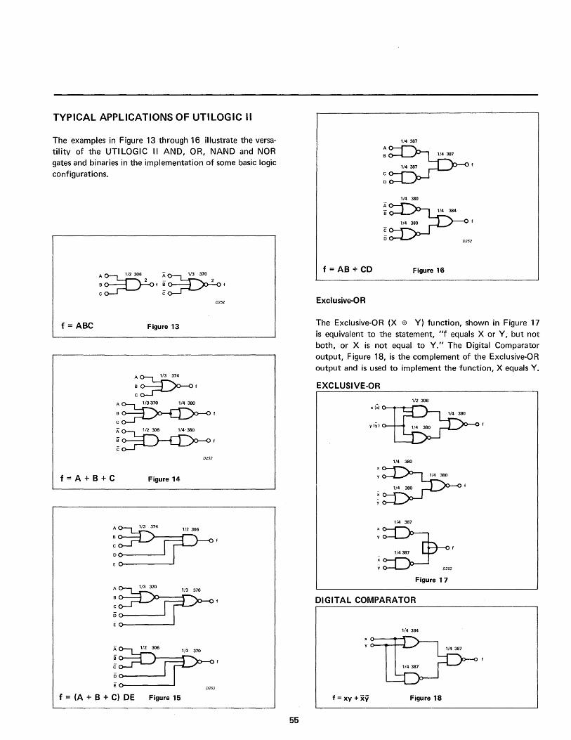
TYPICAL APPLICATIONS OF UTILOGIC II
The examples in Figure 13 through 16 illustrate the versatility of the UTI LOGIC II AND, OR, NAND and NOR gates and binaries in the implementation of some basic logic configurations.
A~/23062 ~~/3 370 2 B f B f
C C
0252
f = ABC Figure 13
A~/3374 B f
C
A~/3370 1/4380
B f
C
~~/2306 1/4-380
B f
C
0252
f=A+B+C Figure 14
~~~. E 0252
f = (A + B + C) DE Figure 15
55
f = AB + CD
Exclusive-OR
A
C
D
A S
c o
1/4 387
1/4 380
Figure 16
The Exclusive-OR (X EI3 V) function, shown in Figure 17 is equivalent to the statement, "f equals X or V, but not both, or X is not equal to V." The Digital Comparator output, Figure 18, is the complement of the Exclusive-OR output and is used to implement the function, X equals V.
EXCLUSIVE-OR
1/2 306
1/4 380
1/4 387
:~. ,~,~~
Figure 17
DIGITAL COMPARATOR
1/4 384
f = xy + xy Figure 18
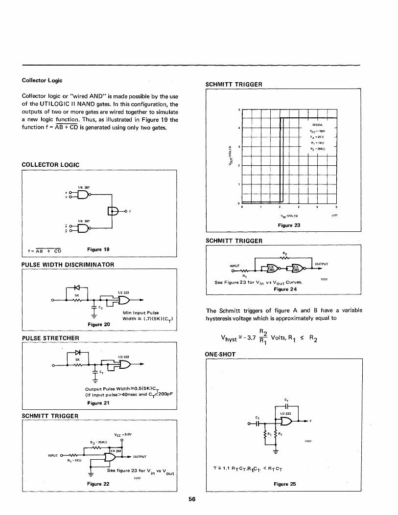
Collector Logic
Collector logic or "wired AND" is made possible by the use of the UTI LOG IC II NAND gates. In this configuration, the outputs of two or more gates are wired together to simulate a new logic function. Thus, as illustrated in Figure 19 the function f = AB + CD is generated using only two gates.
COLLECTOR LOGIC
1/4 387
1/4 387
f= AS + CD Figure 19
PULSE WIDTH DISCRIMINATOR
J cT
Figure 20
PULSE STRETCHER
Min Input Pulse Width ~ ('7)(5K)(C
T)
Output Pulse Width~O.5(5K)CT (if input pulse>40nsec and CT<200pF
Figure 21
SCHMITT TRIGGER
Vcc =5.0V
INPUT O-~Vv-"""'---l(""""""'" OUTPUT
0252
Figure 22
56
SCHMITT TRIGGER
I I I
SP333A
Vee = +5DV
TA = 25°e -R1 = 1Kn
-R2 =20Kn
Oc:=c~==±==±~L-~-l __ l--L~ o
VIN (VOLTS)
Figure 23
SCHMITT TRIGGER
INPUT
~
R1
R2
_~ __ --J. ----.., OUTPUT
1/4 1/4 380 380
0252
See Figure 23 for Vin vs V out Curves.
Figure 24
0252
The Schmitt triggers of figure A and B have a variable hysteresis voltage which is approximately equal to
R2 Vhyst ~ - 3.7 R1 Volts, R 1 ~ R2
ONE-SHOT
C1
o--I~-+--I y
0252
Figure 25
The one-shot of figure 25 operates in the following manner: The input pulse is differentiated by the R, C, network for a positive going input transition. This causes the input to the gate to appear as a logical "1" causing the output to rise. This is fed back to the other input thereby locking the output to a "1" until the voltage at the input discharges through RT CT to the threshold region. At this point the positive feedback restores the output to a logical "0".
The output pulse will have two modes: Mode 1 - if: input p.w. < output p.w. then output p.w. =T Mode 2 - if: input p.w. > output p.w. then output p.w. = input p.w.
This circuit is useful to overcome the contact bounce associated with mechanical to electrical interface and for signal conditioning for short pulse inputs. The same circuit can be built using two NOR gates as shown in figure 28.
ONE SHOT WITH A SCHMITT TRIGGER INPUT, RETRIGGERABLE POSITIVE EDGE TRIGGER
INPUT
10K
RT
INPUT PULSE 0252
_ [RT (10K) + RT(25K) + (25K) (1OK)l
T - 0.7 RT(25K) (10K) J
Figure 26
Circuit operation: When the input rises to a logical "1" level the output of gate 1 assumes a "1" level. This charges CT through the diode thereby presenting the input of gate 2 with a "1". The output of gate 2 therefore assumes a "1" level. This condition holds until the input falls to the input threshold level. At this point, and until the input pulse falls to one diode drop below threshold, the 10 kn resistor feeds current into the input holding a "1" level output.
When the input falls to a diode drop below threshold the current through the 10 kn resistor is "bled" away from the input and the output of gate 1 falls to a logical "0". CT then discharges through the effective parallel resistance until the voltage at gate 2 input reaches threshold. At this time the output falls to a logical zero. CT may be recharged at any point in the cycle by another pulse at the input.
57
RE-TRIGGERABLE ONE-SHOT WITH NEGATIVE EDGE TRIGGERING
Vee.
INPUT 1/2 321
Figure 27
0252
ONE-SHOT WITH COMPLEMENTARY OUTPUTS
10K
RT 8KMAX
y
L..-________ ~ Y
Figure 28
NOISE DISCRIMINATOR ONE-SHOT
NOISE SIGNAL
INPUT JI.._..__ ........
OUTPUT --------il-
~T1 ~ 1.1 R1C1
~T2 ~ 1.1 R2C2
I I I I I ~ 6T114- 6 T2-.j
Figure 29
0252
Circuit Operation: This one-shot discriminates between noise lasting less than time A T 1 and an input signal having a greater than AT 1 duration. An input greater than AT 1 produces an output pulse of AT 2' The output of gate 3 is fed back into the input of gate 1 which guarantees an output pulse of AT 2 if the input goes to "0" during the output "1" cycle. The diodes are used to minimize recovery time.
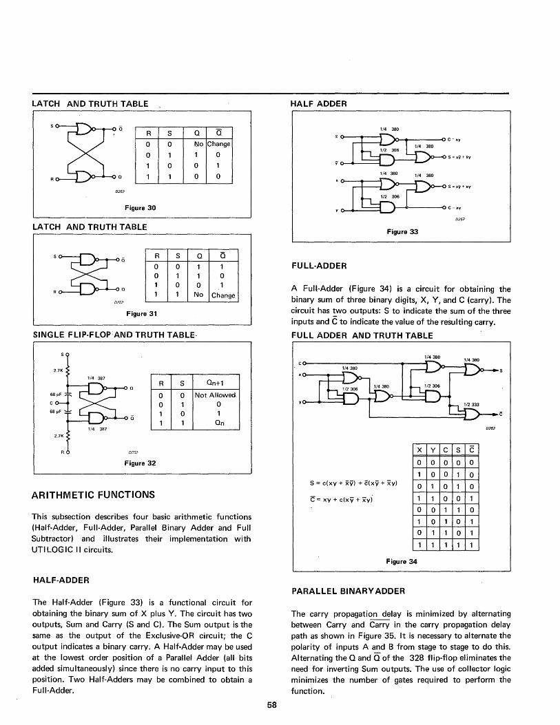
LATCH AND TRUTH TABLE
R
0
0
1
1
0252
Figure 30
LATCH AND TRUTH TABLE
S~Q
R~O 0252
R
0 0 1 1
Figure' 31
S
0
1
0
1
a a No Change
1 0
0 1
0 0
S a 5 0 1 1 1 1 0 0 0 1 1 No Change
SINGLE FLiP-FLOp:AND TRUTH TABLE-
2.7K
1/4 387 R S an+l
0 0 Not Allowed
0 1 0 1 0 1 1 1 an
1/4 387
2.7K
0252
Figure 32
ARITHMETIC FUNCTIONS
This subsection describes four basic arithmetic functions (Half-Adder, Full-Adder, Parallel Binary Adder and Full Subtractor) and illustrates their implementation with UTI LOGIC II circuits.
HALF-ADDER
The Half-Adder (Figure 33) is a functional circuit for obtaining the binary sum of X plus Y. The circuit has two outputs, Sum and Carry (S and C). The Sum output is the same as the output of the Exclusive-OR circuit; the C output indicates a binary carry. A Half-Adder may be used at the lowest order position of a Parallel Adder (all bits added simultaneously) since there is no carry input to this position. Two Half-Adders may be combined to obtain a Full-Adder.
58
HALF ADDER
1/4 380
0252
Figure 33
FULL-ADDER
A FulL-Adder (Figure 34) is a circuit for obtaining the binary sum of three binary digits, X, Y, and C (carry). The circuit has !.wo outputs: S to indicate the sum of the three inputs and C to indicate the value of the resulting carry.
FULL ADDER AND TRUTH TABLE
0252
x y C S C
0 0 0 0 0
1 0 0 1 0 S = c(xy + xv) + c(xy + xv) 0 1 0 1 0
c= xv + c(xy + xv) 1 1 0 0 1
0 0 1 1 0
1 0 1 0 1
0 1 1 0 1
1 1 1 1 1
Figure 34
PARALLEL BINARY ADDER
The carry propagation delay is minimized by alternating between Carry and Carry in the carry propagation delay path as shown in Figure 35. It is necessary to alternate the Rolarity of inputs A and B from stage to stage to do this. Alternating the Q and Q of the 328 flip-flop eliminates the need for inverting Sum outputs. The use of collector logic minimizes the number of gates required to perform the function.
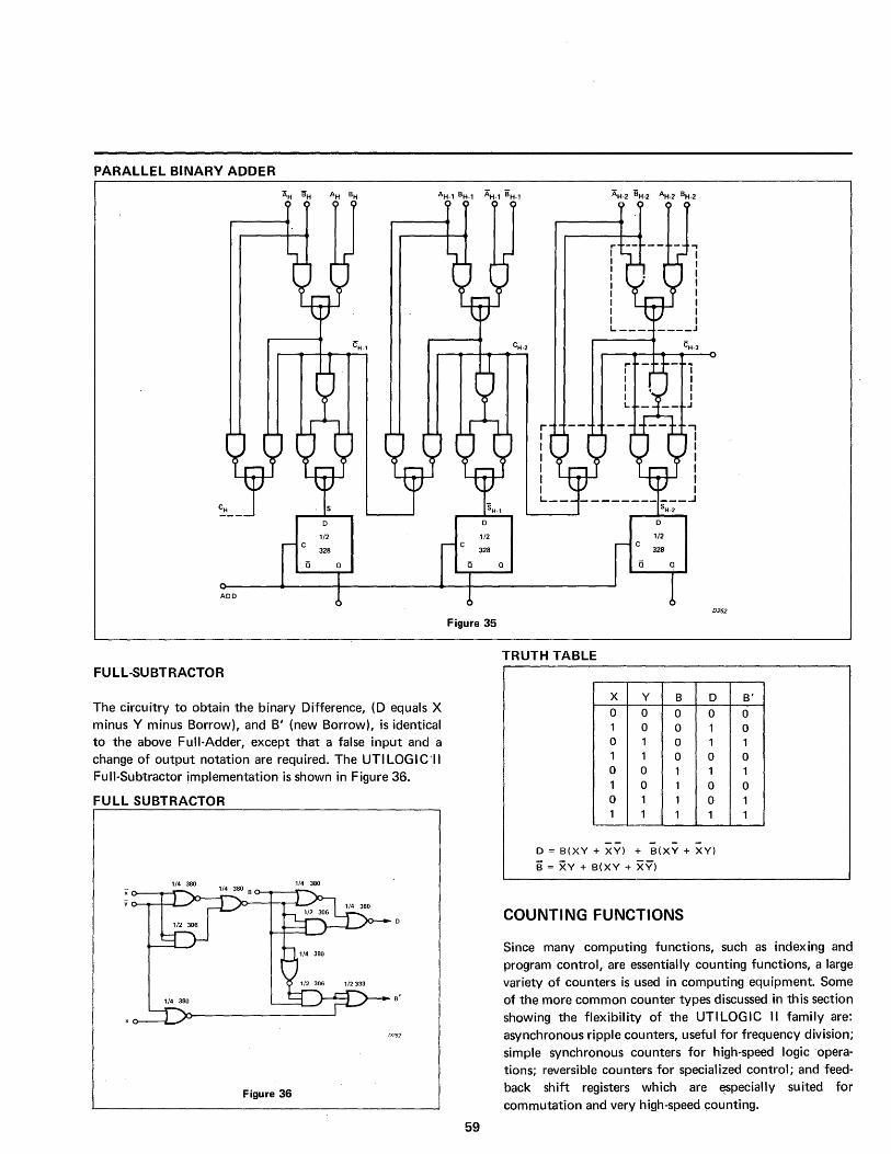
PARALLEL BINARY ADDER
ADD
FULL-SUBTRACTOR
D
1/2
328
o
The circuitry to obtain the binary Difference, (0 equals X minus Y minus Borrow), and B' (new Borrow), is identical to the above Full-Adder, except that a false input and a change of output notation are required. The UTILOGIC'II Full-Subtractor implementation is shown in Figure 36.
FU LL SUBTRACTOR
1/4 380
B'
Figure 36
c
D
1/2
328
Figure 35
59
o
,. I I I I I I I I I L __ _
r -, I I I I I I , I I I I I L _____________ ~
c
SH.2
D
1/2
328
o
TRUTH TABLE
x y 8 0 0 0 1 0 0 0 1 0 1 1 0 0 0 1 1 0 1 0 1 1 1 1 1
- - -
0252
0
0 1 1 0 1 0 0 1
o = B(XV + XV) + B(XV + XV)
B = xv + B(XV + XV)
COUNTING FUNCTIONS
8'
0 0 1 0 1 0 1 1
Since many computing functions, such as indexing and program control, are essentially counting functions, a large variety of counters is used in computing equipment. Some of the more common counter types discussed in this section showing the flexibility of the UTI LOGIC II family are: asynchronous ripple counters, useful for frequency division; simple synchronous counters for high-speed logic operations; reversible counters for specialized control; and feedback shift registers which are ~specially suited for commutation and very hig~-speed counting.
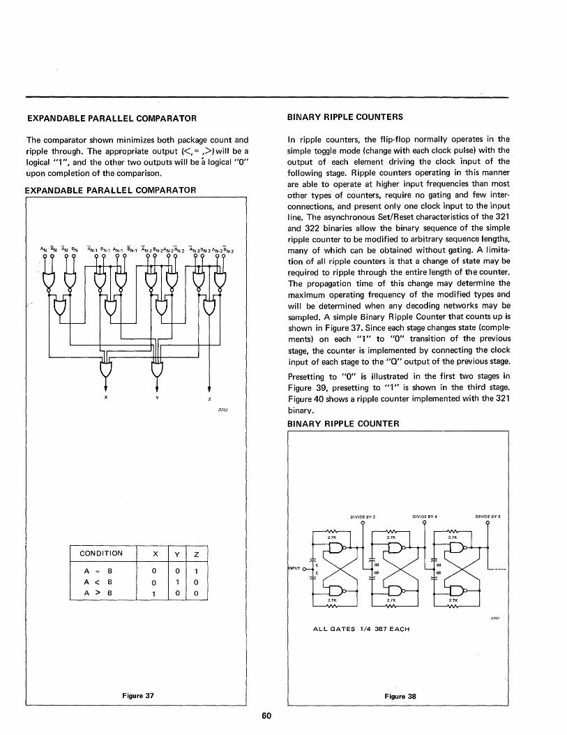
EXPANDABLE PARALLEL COMPARATOR
The comparator shown minimizes both package count and ripple through. The appropriate output «, = ,>) will be a logical "1 ", and the other two outputs will be a logical "0" upon completion of the comparison.
EXPANDABLE PARALLEL COMPARATOR
x y
0252
CONDITION X Y Z
A = B 0 0 1
A < B 0 1 0
A > B 1 0 0
Figyre 37
60
BINARY RIPPLE COUNTERS
In ripple counters, the flip-flop normally operates in the simple toggle mode (change with each clock pulse) with the output of each element driving the clock Input of the following stage. Ripple counters operating in this manner are able to operate at higher input frequencies than most other types of counters, require no gating and few interconnections, and present only one clock input to the input line. The asynchronous Set/Reset characteristics of the 321 and 322 binaries allow the binary sequence of the simple ripple counter to be modified to arbitrary sequence lengths, many of which can be obtained without gating. A limitation of all ripple counters is that a change of state may be required to ripple through the entire I'ength of the counter. The propagation time of this change may determine the maximum operating frequency of the modified types and will be determined when any decoding networks may be sampled. A simple Binary Ripple Counter that counts up is shown in Figure 37. Since each stage changes state (complements) on each "1" to "0" transition of the previous
stage, the counter is implemented by connecting the clock input of each stage to the "0" output of the previous stage.
Presetting to "0" is illustrated in the first two stages in Figure 39, presetting to "1" is shown in the third stage. Figure 40 shows a ripple counter implemented with the 321 binary.
BINARY RIPPLE COUNTER
DIVIDE BY 2 DIVIDE BY 4 DIVIDE BY 8
NPUT o{:
2,7K 2,7K 2,7K
ALL GATES 1/4 387 EACH
Figure 38
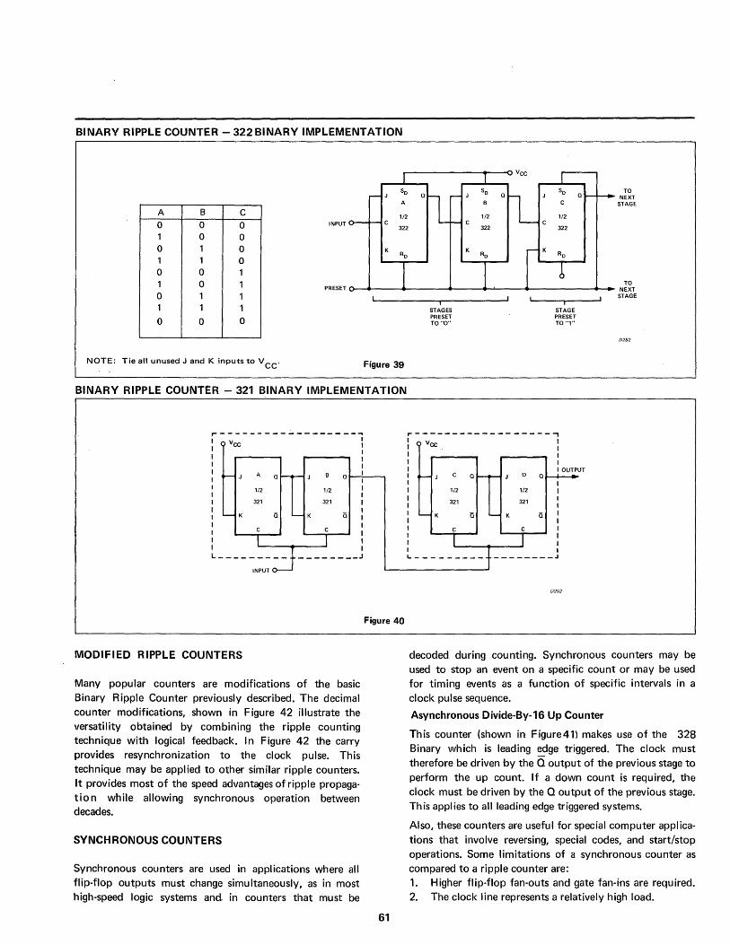
BINARY RIPPLE COUNTER - 322 BINARY IMPLEMENTATION
Vee
So So Q
So Q
TO Q NEXT
A e STAGE
A B C 112 1/2 1/2
0 0 0 INPUT 322 322 322
1 0 0
Ro K
Ro Ro 0 1 0 1 1 0 0 0 1
TO PRESET NEXT
1 0 1 0 1 1 STAGE , t
STAGES STAGE 1 1 1 PRESET PRESET TO "0" TO "1" 0 0 0
0252
NOTE: Tie all unused J and K inputs to V cc. Figure 39
BINARY RIPPLE COUNTER - 321 BINARY IMPLEMENTATION
~------------------~ Vee
~ J A Q ---<r- J Q~--,
- K
1/2
321
I
Q '-- K
1/2
321
I
----~~~~--------
MODIFIED RIPPLE COUNTERS
Many popular counters are modifications of the basic Binary Ripple Counter previously described. The decimal counter modifications, shown in Figure 42 illustrate the versatility obtained by combining the ripple counting technique with logical feedback. In Figure 42 the carry provides resynchronization to the clock pulse. This technique may be applied to other similar ripple counters. It provides most of the speed advantages of ripple propagation while allowing synchronous operation between decades.
SYNCHRONOUS COUNTERS
Synchronous counters are used in applications where all flip-flop outputs must change simultaneously, as in most high-speed logic systems and in counters that must be
Figure 40
61
r------------------, : Vee I I I , ~ J o
OUTPUT Q~ ,
I 1/2 1/2
I I
321 321
, - K '-- K I t , t I I I
~--------- --------~
0252
decoded during counting. Synchronous counters may be used to stop an event on a specific count or may be used for timing events as a function of specific intervals in a clock pulse sequence.
Asynchronous Divide-By-16 Up Counter
This counter (shown in Figure41l makes use of the 328 Binary which is leading ~ge triggered. The clock must therefore be driven by the Q output of the previous stage to perform the up count. If a down count is required, the clock must be driven by the Q output of the previous stage. This applies to all leading edge triggered systems.
Also, these counters are useful for special computer applications that involve reversing, special codes, and start/stop operations. Some limitations of a synchronous counter as compared to a ripple counter are: 1. Higher fl ip-flop fan-outs and gate fan-ins are requ ired. 2. The clock line represents a relatively high load.
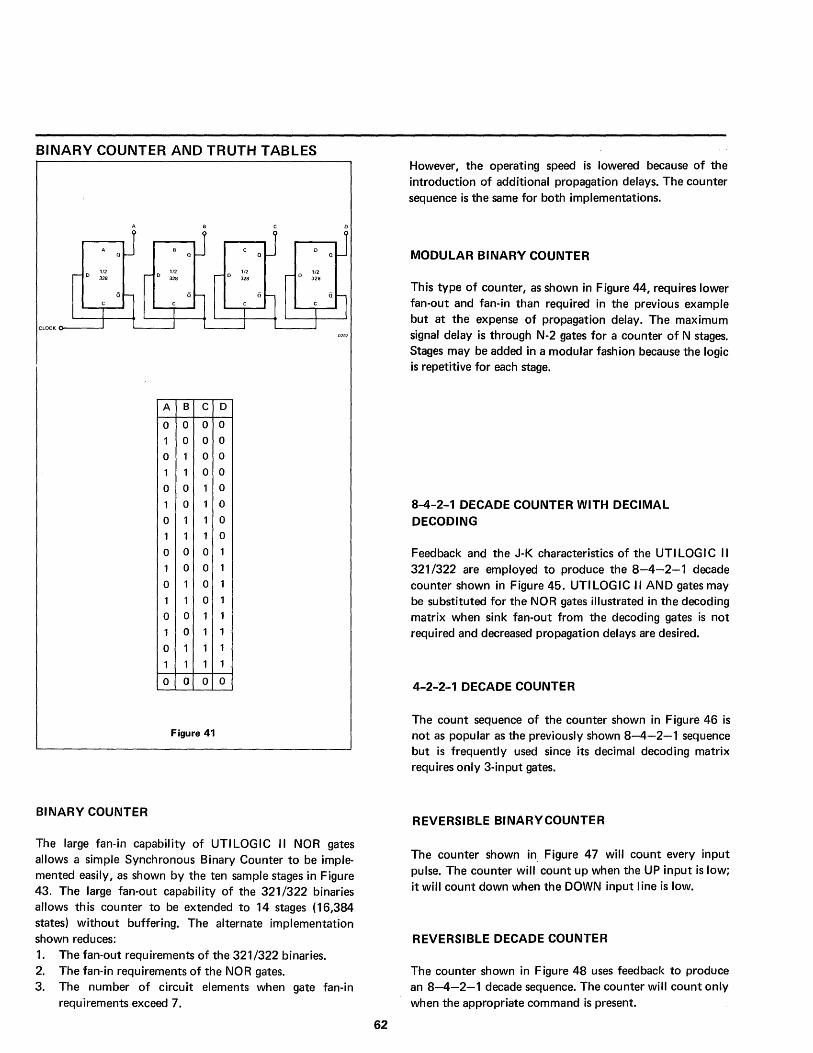
BINARY COUNTER AND TRUTH TABLES
J B C 0
oJ oj aU A B C 0
-0 1/2 r- 0
112 -0
112 -0
112 328 328 328 328
C O~ C O~ C °l C O~ I 1 I
CLOCK ~ J l I I [ I 0252
A 8 C D
0 0 0 0
1 0 0 0
0 1 0 0
1 1 0 0
0 0 1 0
1 0 1 0
0 1 1 0
1 1 1 0
0 0 0 1
1 0 0 1
0 1 0 1
1 1 0 1
0 0 1 1
1 0 1 1
0 1 1 1
1 1 1 1
0 0 0 0
Figure 41
BINARY COUNTER
The large fan-in capability of UTI LOGIC II NOR gates allows a simple Synchronous Binary Counter to be implemented easily, as shown by the ten sample stages in Figure 43. The large fan-out capability of the 321/322 binaries allows this counter to be extended to 14 stages (16,384 states) without buffering. The alternate implementation shown reduces: 1. The fan-out requirements of the 321/322 binaries. 2. The fan-in requirements of the NOR gates. 3. The number of circuit elements when gate fan-in
requirements exceed 7.
62
However, the operating speed is lowered because of the introduction of additional propagation delays. The counter sequence is the same for both implementations.
MODULAR BINARY COUNTER
This type of counter, as shown in Figure 44, requires lower fan-out and fan-in than required in the previous example but at the expense of propagation delay. The maximum signal delay is through N-2 gates for a counter of N stages. Stages may be added in a modular fashion because the logic is repetitive for each stage.
8-4-2-1 DECADE COUNTER WITH DECIMAL DECODING
Feedback and the J-K characteristics of the UT I LOG I C " 321/322 are employed to produce the 8-4-2-1 decade counter shown in Figure 45. UTI LOG IC " AND gates may be substituted for the NOR gates illustrated in the decoding matrix when sink fan-out from the decoding gates is not required and decreased propagation delays are desired.
4-2-2-1 DECADE COUNTER
The count sequence of the counter shown in Figure 46 is not as popular as the previously shown 8-4-2-1 sequence but is frequently used since its decimal decoding matrix requires only 3-input gates.
REVERSIBLE BINARY COUNTER
The counter shown in Figure 47 will count every input pulse. The counter will count up when the UP input is low; it will count down when the DOWN input I ine is low.
REVERSIBLE DECADE COUNTER
The counter shown in Figure 48 uses feedback to produce an 8-4-2-1 decade sequence. The counter will count only when the appropriate command is present.
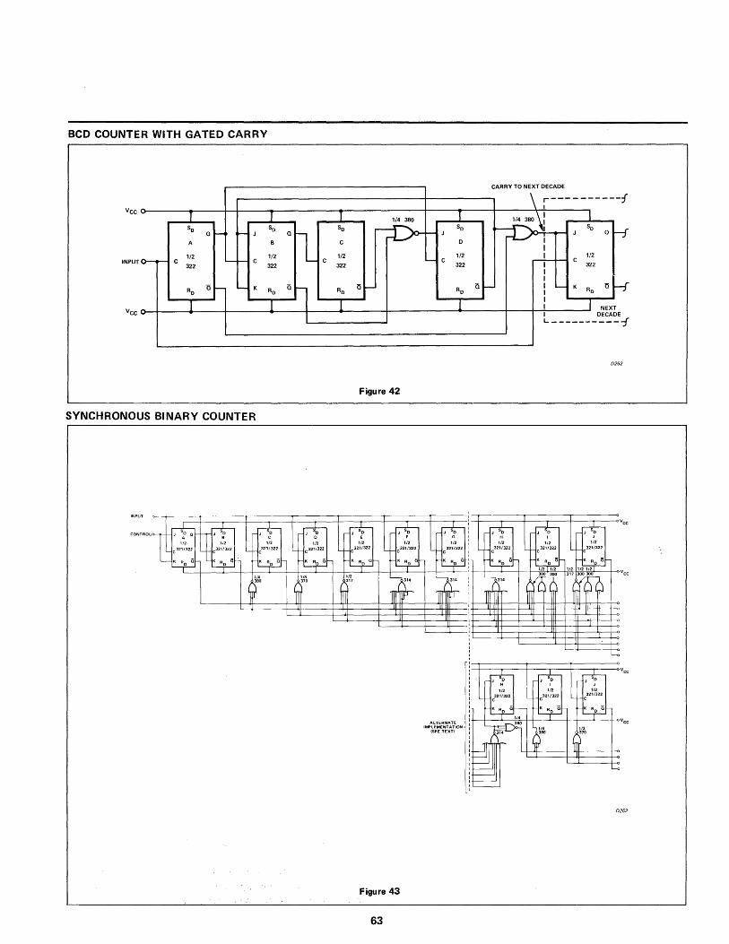
BCD COUNTER WITH GATED CARRY
CARRY TO NEXT DECADE
VCC
\ r----------{
T T T 1/4 380 T
--D-~ I
So - J
So Qrt , So irDo-- So J
So O-{ O- J
A B C D
00-'--<-1/2 1/2 1/2 1/2 1/2
C - - C -C C 322 322 322 322 322 INPUT
RO 0- - K RO 0 f- Ro
O- RO Or- ""'-- K
Ro Ol-f
- 1 I 1 1 I NEXT - DECADE
L - ----------1'
0252
Figure 42
SYNCHRONOUS BINARY COUNTER
.~* ~~ ~ r-J- ~ ~ ~ r---t--- r+- .--+-J g J ~ J ~ J ;' J ~ J D J ~ G I
1/2 1/2 1/2 1/2 1/2 1/2 1/2 1/2 1/2 1/2
C321/32~ C321/322_ . C321/322 C321/322 C
3211322 C321/322 C
321/322 C321/322 C321/322 C
321/322
~ ~ ,K jo Q ~ ,K AID a ,K RID Q ~ ~ K R Q K R a: 1/21°,/2 1/2 1/2'--;nf--
~~t 1/3 1/2
~ '----J,31' 31'
m~ "'~ ~70 ~317 'TIl :r 'TIl
r-
-II 11 II II
-0
...-;-J ~ -+-
J ~ --+-J ~
1/2 1/2 1/2
C321/322 C321/322 C321/322
K RIO a:- K RID Q ~ ALTERNATE 380
IMPLEMENTATION
~. 1/3
(SEE TEXT) 31' 380
~r ~
--0
-
0252
Figure 43
63
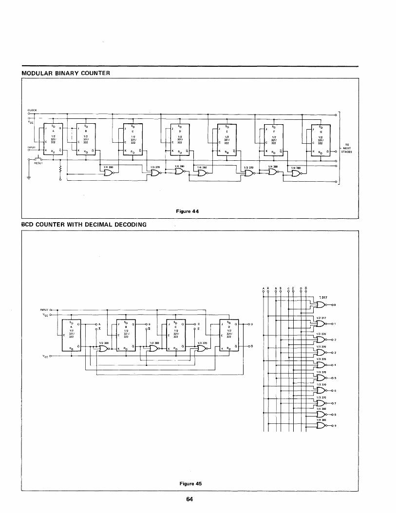
MODULAR BINARY COUNTER
CLOCK
VCC 1 1 1 I ~J
So 01- I--r- J
So r- J
So r- J
So r- J
A B C 0
1/2 1/2 1/2 1/2 321/ 321/ 3211 3211
'--I- C 322 '--I- C 322 '-- r- C 322 '-- f-- C 322 '--t-- C
~ I- K RD Q~ L-K
RO of-- f--K RO oI- l- K RO 01- f--K
-L I I I J
["" 1/4380 113370
~ =u-
Figure 44
BCD COUNTER WITH DECIMAL DECODING
INPUT
Vec
-C
T So
A
1/2 321/ 322
RD
1
1 01-..------.0 A r- J
So
A B
1/2
-I-- C 321/ 322
1/2380 6
~I-K RD
I
1 O~B r- J
So O~C ,--- J
L: C c 1/2
r-C 3211 '--- C 322
~370 Q 0 -K 1~r-K RO IP I I I I
I
Figure 45
64
I T I So
~ J So
r- J So
E F G
112 112 112 3211 3211 3211 322 ,--~e 322 '-f--C 322
TO NEXT
Ro 01- I-K RO 0'- f--K Ro 01-0 STAGES
1 I 1
L 113370
~
AA Bli ec oii
~~ I
So o I--r--<J 0
112 3211
~~ 1/3370
322
RO 01--1-0 ii 113370
T 113370
113370
113370
1/3370
114380
~ ~380
~
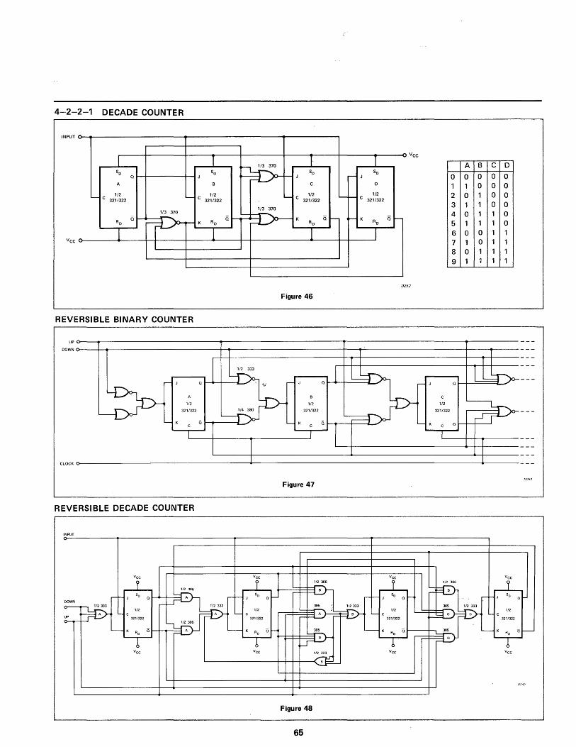
4-2-2-1 DECADE COUNTER
INPUT ,.. -
~
I 1 ~
1 I So So
- J So
r- J So
Q J
A B e 0
A B C D
0 0 0 0 0 1 1 0 0 0
1/2 1/2 - e 1/2 - I--e 112 '--e 321/322 -e 321/322 321/322 321/322
1/3 370 1/3 370
0 - 0 ~ K at-- ~K a r-Ro ~_K Ro Ro Ro
1 1 1 I I
2 0 1 0 0 3 1 1 0 0 4 0 1 1 0 5 1 1 1 0 6 0 0 1 1 7 1 0 1 1 8 0 1 1 1
Vee
9 1 '" 1 1 ,
0252
Figure 46
REVERSIBLE BINARY COUNTER
upo--~~---------------~---------------~-----------------.-------------
OOWNo---~~~-----------------1-~-----------------------1--~~---------------+-----~-------
1/2
321/322
Q I-~t----L"""; Q t--t--====l...-'
CLOCKo-------------------------~-----------------------~-----------------~---------
Figure 47
REVERSIBLE DECADE COUNTER
Vee Vee Vee vf 1 L 1/2 306 L 1/2306
1/2 306 ~ -r--r-
& O..J
.---~ ""-~J
So a
J-~' SO
r-f-- J So at- _~J
So a
OOWN - 1/2333 0---3=£5- 305 1/2333 305 1/2 333
1/2 1/2
"-~~ 1/2 1/2 - e A '-- e _ A _ B '-- e e e ~ e
~-- 321/322 321/322 321/322 321/322 1/2306
-K a A - K 0- 305 - K a 305 _ K o-Ro Ro
P Ro Ro
b b 6 r- D
! Vee Vee 1/2333 Vee Vee
~
02-,7
Figure 48
65
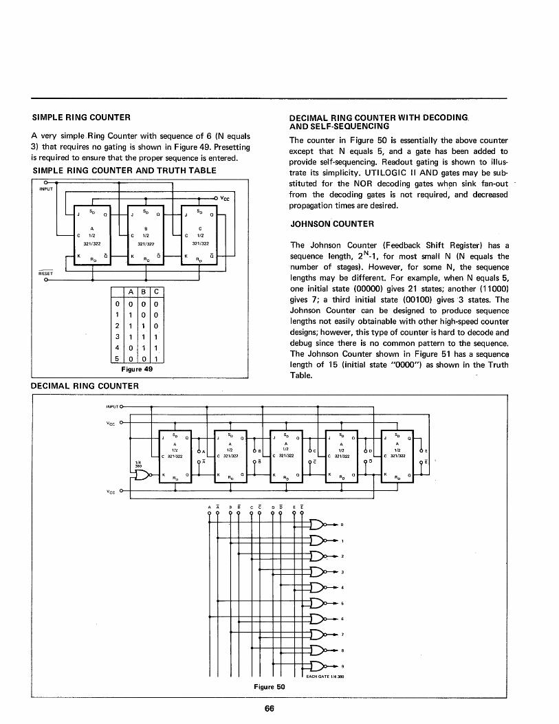
SIMPLE RING COUNTER
A very simple.Ring Counter with sequence of 6 (N equals 3) that requires no gating is shown in Figure 49. Presetting is required to ensure that the proper sequence is entered.
SIMPLE RING COUNTER AND TRUTH TABLE
INPUT
L, - Vee r T T So QI-- I-- J
So QI--I- J So QI--
A B c '--- C 1/2 '--c 1/2 '-- C 1/2
321/322 321/322 3211322
jK a I--- K O~K 01-~ Ro Ro Ro
- T I I RESET T 1 T -
A B C
0 0 0 0
1 1 0 0
2 1 1 0
3 1 1 1
4 0 1 1
5 0 0 1
Figure 49
DECIMAL RING COUNTER
DECIMAL RING COUNTER WITH DECODING1
AND SELF-SEQUENCING
The counter in Figure 50 is essentially the above counter except that N equals 5, and a gate has been added to provide self-sequencing. Readout gating is shown to illustrate its simpli~ity. UTI LOGIC II AND gates may be substituted for the NOR decoding gates wh~n sink fan-out from the decoding gates is not required, and decreased propagation times are desired.
JOHNSON COUNTER
The Johnson Counter (Feedback Shift Register) has a sequence length, 2N-l, for most small N (N equals the number of stages). However, for some N, the sequence lengths may be different. For example, when N equals 5, one initial state (00000) gives 21 states; another (11000) gives 7; a third initial state (00100) gives 3 states. The Johnson Counter can be designed to produce sequence lengths not easily obtainable with other high-speed counter designs; however, th is type of cou nter is hard to decode and debug since there is no common pattern to the sequence. The Johnson Counter shown in Figure 51 has a sequence length of 15 (initial state "0000") as shown in the Truth Table.
INPUT C>----+------..----------<p---------,------,
Vcc 0-~-4_-~---+--~--~~-~---+--~---+-_,
Vcc C>-+----~-------+-----~-----~---t-~
AA as cc DO EE ( -
~ -L -~ -~ ---.... -L
~ I -J -I -
Fr>-EACH GATE 114 380
Figure 50
66
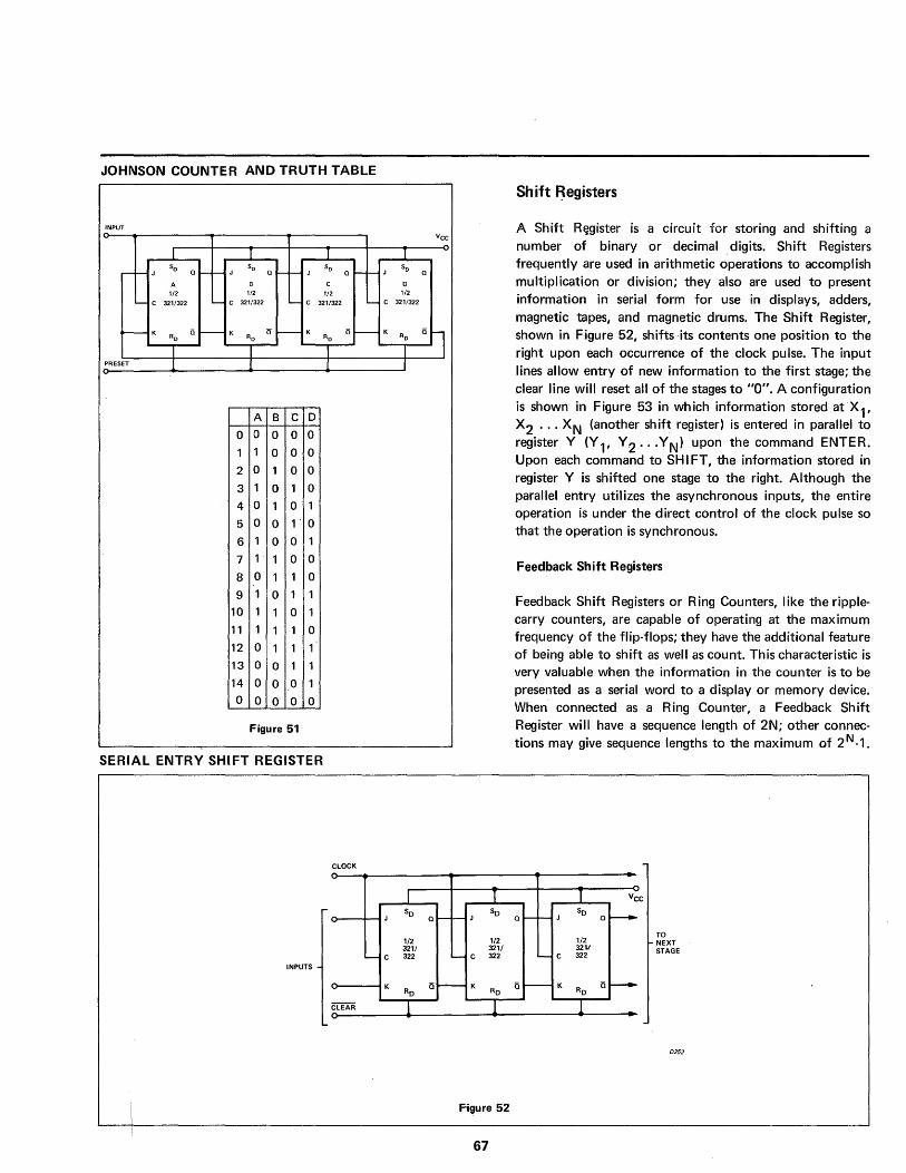
JOHNSON COUNTER AND TRUTH TABLE
INPUT
1 I
- f- J So
o-f- J So
Of-f-- J So
o-f- J
A B e 1/2 1/2 1/2
'--e 321/322 '-- e 321/322 '-- e 3211322 ,--e
~K Ro
5......- K Ro
0" r--- K Ro
5-K
I I PRESET 1 1
A B C 0
0 0 0 0 0
1 1 0 0 0
2 0 1 0 0
3 1 0 1 0
4 0 1 0 1
5 0 0 l' 0
6 1 0 0 1
7 1 1 0 0
8 0 1 1 0
9 1 0 1 1
10 1 1 0 1
11 1 1 1 0
12 0 1 1 1
13 0 0 1 1
14 0 0 0 1
0 0 0 0 0
Figure 51
SERIAL ENTRY SHIFT REGISTER
CLOCK
- J
-c INPUTS
K
mAR
Vee 1">
I So
0
0 1/2
321/322
Ro 5~ I J
I I So
- J So
0-
1/2 1/2 321/ 321/ 322 ~C 322
RO a""-"-'- K
RO
1 1
Figure 52
67
Shift ~egisters
A Shift R~gister is a circuit for storing and shifting a number of binary or decimal ,digits. Shift Registers frequently are used in arithmetic operations to accomplish multiplication or division; they also are used to present information in serial form for use in displays, adders, magnetic tapes, and magnetic drums. The Sh ift Register, shown in Figure 52, shifts its contents one position to the right upon each occurrence of the clock pulse. The input lines allow entry of new information to the first stage; the clear line will reset all of the stages to "0". A configuration is shown in Figure 53 in which information stored at Xl' X2 ... XN (another shift register) is entered in parallel to register Y (Y l' Y 2' .. Y N) upon the command ENTER. Upon each command to SHIFT, the information stored in register Y is shifted one stage to the right. Although the parallel entry utilizes the asynchronous inputs, the entire operation is under the direct control of the clock pulse so that the operation is synchronous.
Feedback Shift Registers
Feedback Shift Registers or Ring Counters, like the ripplecarry counters, are capable of operating at the maximum frequency of the flip-flops; they have the additional feature of being able to shift as well as count. This characteristic is very valuable when the information in the counter is to be presented as a serial word to a display or memory device. When connected as a Ring Counter, a Feedback Shift Register will have a sequence length of 2N; other connections may give sequence lengths to the maximum ,of 2 N ·1.
T
or- - J So
1/2 321/
-c 322
a r----- K RO
1
Vc C
0-
Q r---
TO NEXT STAGE
0252
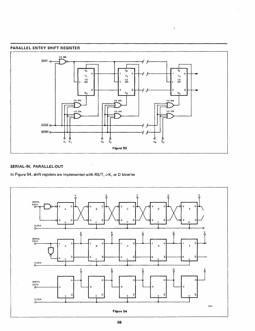
PARALLEL ENTRY SHIFT REGISTER
1/4 380
1/3 374
Y1
1/2 322
Q t-+----_+_-I
Q t-+---------I K
Y2
1/2 322
~o-~----4-~_+_--------------------~_+_+-----------------------~
~o-------------~_+_--------------------------~~+--------------------~
X1 X 1
Figure 53
SERIAL-IN. PARALLEL-OUT
In Figure 54, shift registers are implemented with RS/T. J-K. or 0 binaries
SERIAL DATA
CLOCK
RIAL SE
D ATA
A
A
Q A
Q
A (~
Q~
Q Q C
K Q Q C
(~ (~
Q ----1 Q~
K
D '-- D ~D '-- D -C
Q C
Q C
Q
CLOCK 1 1 1 .
Figure 54
68
D
C
C
1
1/3 374
D
D
Q
Q
D
Q-
Y3
112 322
K
Q
'--- D
Q
Q
Q
C Q
I 0252
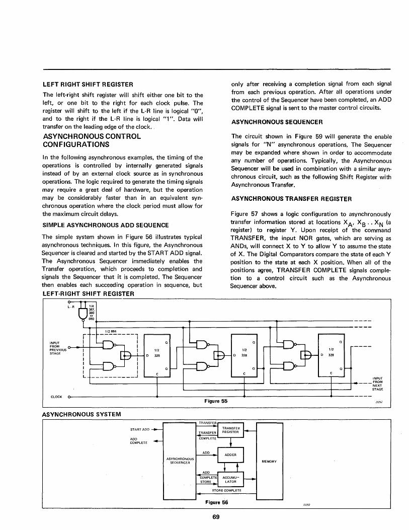
LEFT RIGHT SHIFT REGISTER
The left-right shift register will shift either one bit to the left, or one bit to the right for each clock pulse. The register will shift to the left if the L-R line is logical "0", and to the right if the L-R line is logical "1". Data will transfer on the leading edge of the clock. ,
ASYNCHRONOUS CONTROL CONFIGURATIONS
In the following asynchronous examples, the timing of the operations is controlled by internally generated signals instead of by an external clock source as in synchronous operations. The logic required to generate the timing signals may require a great deal of hardware, but the operation may be considerably faster than in an equivalent synchronous operation where the clock period must allow for the maximum circuit delays.
SIMPLE ASYNCHRONOUS ADD SEQUENCE
The simple system shown in F jgure 56 illustrates typical asynchronous techniques. In this figure, the Asynchronous Sequencer is cleared and started by the START ADD signal. The Asynchronous Sequencer immediately enables the Transfer operation, which proceeds to completion and signals the Sequencer that it is completed. The Sequencer then enables each succeeding operation in sequence, but
LEFT-RIGHT SHIFT REGISTER
1/4 387, 380 Or
only after receiving a completion signal from each signal from each previous operation. After all operations under the control of the Sequencer have been completed, an ADD COMPLETE signal is sent to the master control circuits.
ASYNCHRONOUSSEOUENCER
The circuit shown in Figure 59 will generate the enable signals for "N" asynchronous operations~ The Sequencer may be expanded where shown in order to accommodate any number of operations. Typically, the Asynchronous Sequencer will be used in combination with a similar asynchronous circuit, such as the following Shift Register with Asynchronous Transfer.
ASYNCHRONOUS TRANSFER REGISTER
Figure 57 shows a logic configuration to asynchronously transfer information stored at locations XA , X B .. X N (a register) to register Y. Upon receipt of the command TRANSFER, the input NOR gates, which are serving as ANDs, will connect X to Y to allow Y to assume the state of X. The Digital Comparators compare the state of each Y position to the state at each X position. When all of the positions agree, TRANSFER COMPLETE signals completion to a control circu it such as the Asynchronous Sequencer above.
ooo~ ________________________ ~ ______________________ ~r-__________________ __
1/2884 - ---------1 INPUT FROM PREVIOUS STAGE
I Q
I I . 1/2
"'-I--I~ D 328 I I I I __________ .J C
CLOCK
ASYNCHRONOUS SYSTEM
START ADD --......-
ADD ---COMPLETE
Q
ASYNCHRONOUS SEQUENCER
Q Q
1/2 1/2
D 328 D 328
Q Q
C
INPUT
L..---------------+---t---- - ~~~~ STAGE
Figure 55 0252
TRANSFER,
: I TRANSFER J.--TRANSFER REGISTER
COMPLETE
~ ADD I ADDER I I MEMORY
• t ADD
COMPLETE' ACCUMU-r STORE LATOR
STORE COMPLETE
Figure 56 D252
69
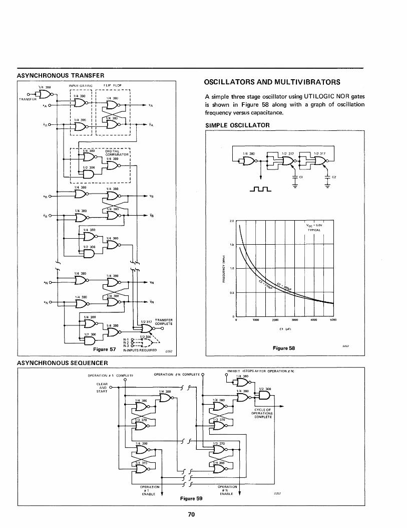
ASYNCHRONOUS TRANSFER
i/4 380 INPUT GATING FLIP FLOP
~-- - i74-380--- DIGiTAL--l I COMPARATOR I
1/4 380 I
I I I I
I I L _______________ J
1/4 380
Figure 57 N.INPUTS REQUIRED 0252
ASYNCHRONOUS SEQUENCER
OPERATION It 1 COMPLETE OPERATION # N COMPLETE
CLEAR AND o-~-+-------------------4
START
OPERATION 1f1
ENABLE
1/4 380
Figure 59
70
OSCILLATORS AND MUL TIVIBRATORS
A simple three stage oscillator using UTI LOGIC NOR gates is shown in Figure 58 along with a graph of oscillation
frequency versus capacitance.
SIMPLE OSCI LLATOR
2.0
1.5
1.0
0.5
o o
OPERATION #N
ENABLE
\ \ ~
'\ ~ ~~ ~ S,O",.<-
i':::::.]~ -.; ::::::::
1000 2000 3000
Cl (pFI
Figure 58
0252
I Vee = 5.0V
TYPICAL
r===-~ ~
4000 5000
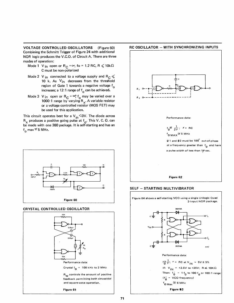
VOLTAGE CONTROLLED OSCILLATORS (Figure 60) Combining the Schmitt Trigger of Figure 24 with additional NOR logic produces the V.C.O. of Circuit A. There are three modes of operation:
Mode 1 V in open or RC =00, fo = 1.2 RC, R "10kn C must be non-polarized
Mode 2 V in connected to a voltage supply and RC ~ 10 k. As Vin decreases from the threshold region of Gate 1 towards a negative voltage fo increases; a 12:1 range of fo can be achieved.
Mode 3 V in open or RC = oe: fo may be varied over a 1000: 1 range by varying Rx. A variable resistor or a voltage controlled resistor (MOS FET) may be used for this application.
This circuit operates best for a V in <OV. The diode across Rx produces a positive going pulse at f o. This V. C. O. can be made with one 380 package. It is self-starting and has an fo max-=' 5 MHz.
fo
INPUT
Figure 60
CRYSTAL CONTROLLED OSCILLATOR
10K
10K
Performance data:
Crystal fa = 100 kHz to 2 MHz
RW controls the amount of positive
feedback permitting both sinusoidal
and square-wave operation.
Figure 61
71
RC OSCILLATOR - WITH SYNCHRONIZING INPUTS
~ !2!1 ~-,.-
I I I I L-r--------...J I !2! 2 o- __ ...... ______________ ...J
Performance data:
f E:t ...l. 1'= RC a 2r'
fa MAX~ 5 MHz
(J 1 and 02 must be 1800
out-of-phase
at a frequency greater than fa and have
a pulse width of less than 1f sec.
Figure 62
SELF - STARTING MULTIVIBRATOR
Figure 64 shows a self-starting VCO using a single Utilogic Quad 2-lnput NOR package.
IN914A
Performance data:
f8+-' T = RC at VIN
= 5V± 5%
If: VIN
= +2.5V to +25V; R ~ 10Kn
Then: fO = 1 fa to. 100 fa or 100: 1 range
(fO = VCO frequency)
fa Max ~ 5 MHz
Figure 63
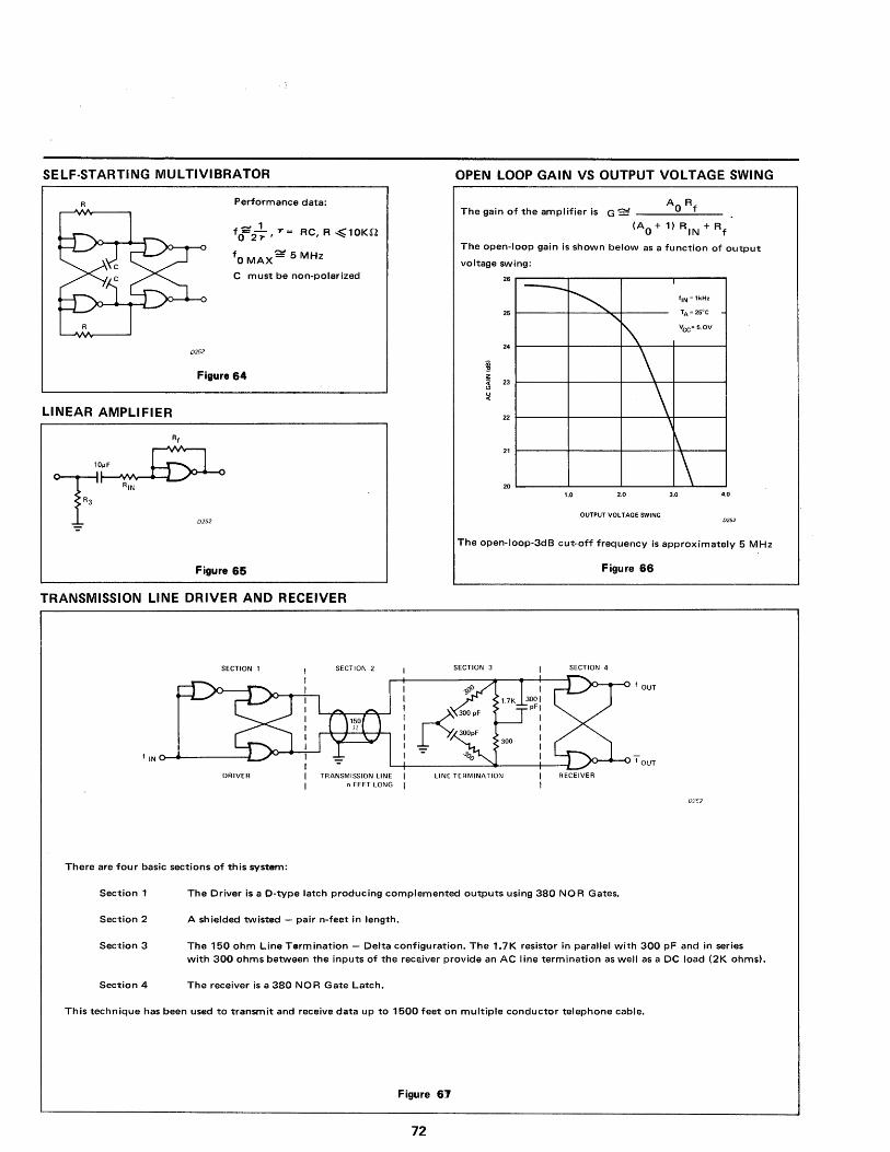
SELF-STARTING MULTIVIBRATOR OPEN LOOP GAIN VS OUTPUT VOLTAGE SWING
Performance data:
_1 fO==ir I -r = RC, R ~10Kn.
fO MAX 9t 5 MHz
C must be non-polarized
0252
Figure 64
LINEAR AMPLIFIER
Figure 65
AO Rf The gain of the amplifier is G s:! ___ ....;;;........:.. __
(AO + 1) RIN + R f
The open-loop gain is shown below as a function of output
voltage swing:
26 I
25
24
~ z ::( 23 (!)
~
22
---~ 'IN = 1kHz
'1\ TA = 25"e
Vee= 5.0V
\ \
\
21
20
\
\ 1.0 2.0 3.0 4.0
OUTPUT VOLTAGE SWING 0252
The open-loop-3dB cut-off frequency is approximately 5 MHz
Figure 66
TRANSMISSION LINE DRIVER AND RECEIVER
SECTION 1 SECTION 2 SECTION 3 SECTION 4
, OUT
, IN o-.... -------L~ L-+-______ ~_--+-_1~/':>-...... -O f OUT
DRIVER
There are four basic sections of this system:
TRANSMISSION LINE n FEET LONG
LINE TERMINATION RECEIVER
Section 1 The Driver is a D-type latch producing complemented outputs using 380 NOR Gates.
Section 2 A shielded twisted - pair n-feet in length.
0252
Section 3 The 150 ohm Line Termination - Delta configuration. The 1.7K resistor in parallel with 300 pF and in series with 300 ohms between the inputs of the recaiver provide an AC line termination as well as a DC load (2K ohms).
Section 4 The receiver is a 380 NOR Gate Latch.
This technique has been used to transmit and receive data up to 1500 feet on multiple conductor telephone cable.
Figure 6'7
72
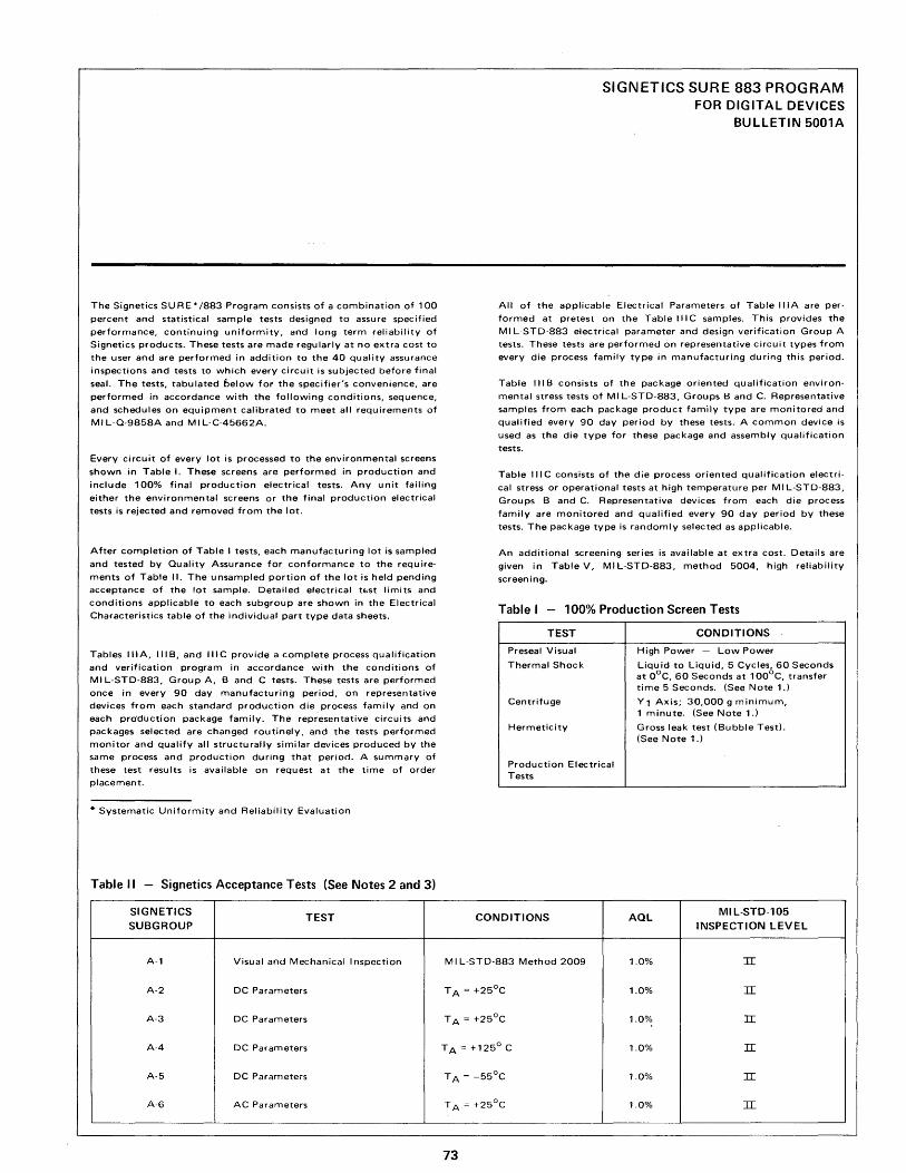
The Signetics SU R E' /883 Program consists of a combination of 100
percent and statistical sample tests designed to assure specified
performance, continuing uniformity, and long term reliability of
Signetics products. These tests are made regularly at no extra cost to
the user and are performed in addition to the 40 quality assurance
inspections and tests to which every circuit is subjected before final
seal. The tests, tabulated below for" the specifier's convenience, are
performed in accordance with the following conditions, sequence,
and schedules on equipment calibrated to meet all requirements of
MI L-Q·9858A and MI L-C-45662A.
Every circuit of every lot is processed to the environmental screens
shown in Table I. These screens are performed in production and
include 100% final production electrical tests. Any u nit failing
either the environmental screens or the final production electrical
tests is rejected and removed from the lot.
After completion of Table I tests, each manufacturing lot is sampled
and tested by Quality Assurance for conformance to the require
ments of Table II. The unsampled portion of the lot is held pending
acceptance of the lot sample. Detailed electrical tbSt limits and
conditions applicable to each subgroup are shown in the Electrical
Characteristics table of the individual part type data sheets.
Tables III A, III B, and III C provide a complete process qualification
and verification program in accordance with the conditions of
MI L-STD-883, Group A, Band C tests. These tests are performed
once in every 90 day manufacturing period, on representative
devices from each standard production die process family and on
each pro'dUttion package family. The representative circuits and
packages selected are changed routinely, and the tests performed
monitor and qualify all structurally similar devices produced by the
same process and production during that period. ,0... summary of
these test results is available on request at the time of order
placement.
* Systematic Uniformity and Reliability Evaluation
Table II - Signetics Acceptance Tests (See Notes 2 and 3)
SIGNETICS TEST SUBGROUP
A-1 Visual and Mechanical Inspection
A-2 DC Parameters
A-3 DC Parameters
A-4 DC Parameters
A-5 DC Parameters
A-6 AC Parameters
SIGNETICS SURE 883 PROGRAM FOR DIGITAL DEVICES
BULLETIN 5001A
All of the applicable Electrical Parameters of Table IliA are per·
formed at pretest on the Table III C samples. This provides the
MI L-STD-883 electrical parameter and design verification Group A
tests. These tests are performed on representative circuit types from
every die process family type in manufacturing during this period.
Table III B consists of the package oriented qualification environ
mental stress tests of MI L-STD-883, Groups Band C. Representative
samples from each package product family type are monitored and
qualified every 90 day period by these tests. A common device is
used as the die type for these package and assembly qualification
tests.
Table III C consists of the die process oriented qualification electri
cal stress or operational tests at high temperature per MI L-STD-883,
Groups Band C. Representative devices from each die process
family are monitored and qualified every 90 day period by these
tests. The package type is randomly selected as applicable.
An additional screening series is available at extra cost. Details are
given in Table V, MIL-STD-883, method 5004, high reliability
screening.
Table I - 100% Production Scr-een Tests
TEST CONDITIONS
Preseal Visual High Power - Low Power
Thermal Shock Liqu id to Liqu id, 5 Cycles, 60 Seconds at OoC, 60 Seconds at 100°C, transfer time 5 Seconds. (See Note 1.)
Centrifuge Y1 Axis; 30,000 g minimum, 1 minute. (See Note 1.)
Hermeticity Gross leak test (Bubble Test). (See Note 1.)
Production Electrical Tests
CONDITIONS AQL MIL·STD·105 INSPECTION LEVEL
MI L-STD-883 Method 2009 1.0% :II
T A = +25O
C 1.0% IT
T A = +25O
C 1.0% IT
T A = +125° C 1.0% IT
T A = -55°C 1.0% IT
T A = +250
C 1.0% IT
73
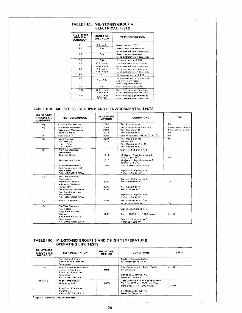
TABLE IliA. MIL-STD-883 GROUP A ELECTRICAL TESTS
Mll-STD·883 SIGNETICS GROUP A SUBGROUP TEST DESCRIPTION
SUBGROUP
Al A-2, A·3 Static tests at 25°C
A2 A4 Static tests at ma)(imum rated operating temperature.
A3 A-5 Static tests at minimum rated operating temperature.
A4 A6 Dynamic tests at 25°C,
A5 C 2, when Dynamic tests at ma)(imum applIcable rated operating temperature.
A6 C 2, when Dynamic tests at minimum applIcable rated operating temperature.
A7 FunctIonal tests at 25°C.
A8 Functlbnal tests at ma)(lmum A 4, A 5 and minImum rated
operating temperatures.
A9 A6 Switching tests at 25°C.
A10 C 2, when SWitching tests at maximum applicable rated operating temperature.
f----- All C 2, when SWltchong tests at minImum applicable rated operatIng temperature.
TABLE IIIB. MIL-STD-883 GROUPS BAND C ENVIRONMENTAL TESTS
Mll-STD-883 Mll-STD-883 GROUP B & C TEST DESCRIPTION METHOD
CONDITIONS SUBGROUP
'Bl Physical D,mensions 2008 Test CondItIon A
B2 MarkIng Permanency 2008 . Test ConditIon B, Para 3,2,1 Visual and Mechanical 2008 Test Condition B Bond Strength 2011 Test Condition 0
B3 Solderability 2003 Solder Temperature 260°C ±10oC
B4 Lead FatIgue 2004 Test CondItIon B2 Hermetlcity 1014 See Note 4
a. F,ne Test CondItion A or B
b. Gross Test Condition C
Cl Pre· Test Electrical Signetics Subgroup A-3 Parameters Thermal Shock 1011 15 Cycles. Test ConditIon C,
+ 150°C to -65°C Temperature Cycle 1010 10 Cycles. Test CondItIon C,
150°C to -65°C MOISture Resistance 1004 OmIt Initial condItIoning. End Point Electrical Parameters Signetics Subgroup A'3 FAI LURE CRITERIA Refer to Table IV.
C2 Pre· Test Electrical Paramete~s Signetics Subgroup A'3 Mechanical Shock 2002 Test CondItIon B VibratIon Variable Frequency 2007 Test CondItIon A Constant Acceleration 2001 Test CondItion E End Point Electrical Parameters Signetics Subgroup A·3 FAILURE CRITERIA Refer to Table IV.
C3 Salt Atmosphere 1009 Test Condition A. Omit initial condItIoning.
C4 Pre- Test Electrical Parameters , Signetics Subgroup A·3 High Temperature Storage 1008 TA = +150
oC, t ~ 1000 hours
End POInt Electrocal Parameters Slgnetics Subgroup A-3 FAI LURE CRITERIA Refer to Table IV.
TABLE IIIC. MIL-STD-883 GROUPS BAND C HIGH TEMPERATURE OPERATING LIFE TESTS
Mll-STD-883 Mll-STD-883 GROUPB & C TEST DESCRIPTION CONDITIONS SUBGROUP METHOD
Pre- Test ai,d Design Table III A as applicable, Verification Electrical data sheet groups A & C. Parameters
Cs High Temperature Steady Test Condition A T A = 150°C State Reverse Bias 1015 t = 72 hours. End Point Electrical Parameters Signetics Subgroup A-3
FAI LURE CRITERIA Refer to Table IV
85 & C5 High Temperature Test Condition 0 or E as applicable. Operating Life 1005 T A = + 125°C or +850 C, per Part
Data Sheet. t= 1000 hours. End Poont Electrical Parameters Signetics Subgroup A-3 FAILURE CRITERIA Refer to Table IV.
it Slgnetlcs performs a truth table test.
74
lTPD
15
4 devIces/no faIlure 1 device/no faIlure 15
15
15
15
15
15
A = 15
lTPD
A = 10
A = 10
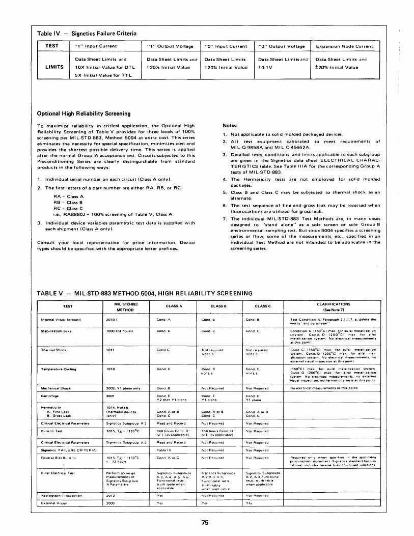
Table IV - Signetics Failure Criteria
TEST "1" Input Current "1" Output Voltage
Data Sheet Limits and' Data Sheet Limits and'
LIMITS lOX Initial Value for DTL ±20% Initial Value
5X Initial Value for TTL
Optional High Reliability Screening
To maximize reliability in critical application, the Optional High
Reliability Screening of Table V provides for three levels of 100%
screening per MI L·STO-883, Method 5004 at extra cost. This series
eliminates the necessity for special specification, minimizes cost and
provides the shortest possible -delivery time. This series is applied
after the normal Group A acceptance test. Circuits subjected to this
Preconditioning Series are clearly distingu ishable from standard
products in the following ways:
1. Individual serial number on each circuit (Class A only).
2. The first letters of a part number are either RA, RB, or RC.
RA = Class A
RB = Class B
RC = Class C
i.e., RA8880J = 100% screening of Table V, Class A.
3. Individual device variables parametric test data is supplied with
each shipment (Class A only).
Consult your local representative for price information. Device
types should be specified with the appropriate letter pr.efixes.
"0" Input Current "0" Output Voltage Expansion Node Current
Data Sheet Limits Data Sheet Limits and Data Sheet Limits and
±20% Initial Value ±O.lV ±20% Initial Value
Notes:
1. Not applicable to solid molded packaged devices.
2. A II test equipment calibrated to meet requ irements of
MI L-Q-9858A and MI L-C-45662A.
3. Detailed tests, conditions, and limits applicable to each subgroup
are given in the Signetics data sheet ELECTRICAL CHARAC
TERISTICS table. Sea Table IliA for the corresponding Group A
tests of MI L-STO-883.
4. The Hermeticity tests are not employed for solid molded
packages.
5. Class B and Class C may be subjected to thermal shock as an
alternate.
6. The test sequence of fine and gro!'s leak may be reversed when
fluorocarbons are utilized for gross leak.
7. The individual MI L-STD-883 Test Methods are, in many cases
designed to "stand alone" as a sole screen or sole Group B
environmental sampling test. But since 5004 specifies a screening
series or flow, some of the measurements, etc., spec;fied in an
individual Test Method are not intended to be applicable in the
screening series.
TABLE V - MIL·STD·883 METHOD 5004, HIGH RELIABILITY SCREENING
TEST
Internal Visual (preseal)
Stabilization Bake
Thermal Shock
Tempelature Cycling
MechanIcal Shock
Centrifuge
Hermeticity
A. Fine Leak B. Gross Leak
Critical Electrical Parameters
Critical Electrical Parameters
Signetics FAIL.URE CRITERIA
Rev.rse Bias ,Burn In
Final Electncal Test
Radiographic Inspection
Ex ternal Visual
MI L-STO-883
METHOD
2010.1
1008 (24 hours)
1011
1010
2002. Yl plane only
2001
1014. Note6
(HermetIc deVICes only)
Signetics Subgroup A·3
Slgnetlcs Subgroup A 3
1015. TA - "50o C t ;,. 72 hours
Perform go no go measurements of Signetics Subgroup A Parameters
2012
2009
CLASS A
Cond A
Cond C
Cond C
Condo C
Condo B
Cond E Y2 then Y 1 plane
Condo A or B Condo C
Read and Record
240 hours Condo 0 or E (as applIcable)
Read and Record
Table I V
Cond A or C
Signetics Subgroups
A 2. A 4. A 5. A 6. Functional tests. truth table when applicable
Yes
Yes
CLASS B
Condo B
Condo C
Not required
NOTE I)
Cond C
NOTE 5
Not Required
Cond E Y 1 plane
Condo A or B Condo C
Not Required
168 hours Cond . .o or E (as applicable)
Not ReqUired
Not ReqUired
Not ReqUired
Signetics Subgroups A 2.A 3. A 6.
Functional tests.
truth table when applicable
Not ReqUired
Yes
75
CLASS C
Condo B
Condo C
Not required. NOTE 5
Condo C
NOTE 5
Not ReqUired
Condo E Y 1 plane
Cond A or B Condo C
Not Required
Not ReqUired
Not ReqUired
Not ReqUired
Not ReqUired
Signetics Subgroups A 2, A 3 Functional tests, truth table when applicable
Not ReqUired
Yes
CLARIFICATIONS
(Sw Note 7)
Test CondItion A. Paragraph 3.1.1.7. a. delete the words "and parameter"
CondItion C (150°C) max. tor aulal metallizatIOn system. Condo 0 (200 C) max. for al/al metallization system. No electrical measurements at thiS POint.
Condo C (150°C) max. for au/al .,..etalllZatlon system. Cond.D (200°C) max. for al/al met· allization system. No electrical measurements. no external VIsual inspection at thiS pOint.
(150°C) max. for au/al metallization system. Cond.D (200°C) max. for al/al metelllZatlon system No electrical me.surements, no external visual Inspection, no hermetlclty tests at thiS point.
No electrical measurements at this point.
ReqUired only when specified In the applicable
procure',ment document Signetrcs standard burn-In (above) Includes reverse bias of unused Junctions
· .. J .
SALES OFFICES
• New England Regional Sales Office: Miller Building, Suite 11 594 Marrett Road, Lexington, Massachusetts 02173 Phone (617) 861-0840 TWX: (710) 326-6711
• Atlantic States Regional Sales Office: 2460 Lemoine Ave., Fort Lee, New Jersey 07024 Phone: (201) 947-9870 TWX: (710) 991-9794
Florida: 3267 San Mateo, Clearwater 33515 Phone: (813) 726-3469 TWX: (810) 866-0437
Florida: 4347 Northwest 2nd Court Boca Raton, Florida 33432 Phone: (305) 391-8318 TWX: (510) 953-7538
Maryland: Silver Springs Phone: (301) 946-6030
Pennsylvania and Southern New Jersey: P. O. Box 431 Oakwood Drive, Medford, New Jersey 08055 Phone: (609) 665-5071
Virginia: 12001 Whip Road, Reston 22070 Phone: (301) 946-6030
• Central Regional Sales Office: 5105 Tollview Drive, Suite 209 Rolling Meadows, Illinois 60008 Phone: (312) 259-8300 TWX: (910) 687-0765
Minnesota: 7710 Computer Ave., Suite 132, Minneapolis 55435 Phone: (612) 922-2801 TWX: (910) 576-2740
Ohio: 3300 So. Dixie Drive, Suite 220, Dayton 45439 Phone: (513) 294-8722
• Northwest Regional Sales Office: 811 E. Arques, Sunnyvale, CA 94086 Phone (408) 739-7700 TWX: (910) 339-9220 (910) 339-9283
• Southwest Regional Sales Office: 2061 Business Center Dr. Suite 214, Irvine, CA 92664 Phone: (714) 833-8980, (213) 437-6718 TWX: (910) 595-1506
California: P. O. Box 788, Del Mar 92014 Phone: (714) 453-7570
REPRESENTATIVES
ALABAMA Huntsville 35801: Compar Corp., 904 Bob Wallace Ave., Suite A Phone: (205) 539-8476
ARIZONA Scottsdale 85252: Compar Corp., Box 1607 Phone: (602) 947-4336 TWX: (910) 950-1293
CALIFORNIA San Diego 92123: Celtee Company, Inc., 8799 Balboa Avenue Phone: (714) 279-7961 TWX: (910) 335-1512
CANADA Toronto 17, Ontario: Corning Glass Works of Canada, Ltd., 135 Vanderhoff Ave. Phone: (416) 421-1500 TWX: (610) 491-2155
Montreal 265, Quebec: Corning Glass Works of Canada, 7065 Chester Ave.
COLORADO Denver 80237: Parker Webster Company, 8213 E. Kenyon Dr. Phone: (303) 770-1972
CONN ECTI,CUT Hamden 06518: Compar Corp., P. O. Box 5204 Phone: (203) 288-9276 TWX: (710) 465-1540
FLORIDA Altamonte Springs 32701: WMM Associates, Inc., 515 Tivoli Ct. Phone: (305) 831-4645
Clearwater 33516: WMM Associates, Inc., 1260A S. Highland Ave. Phone: (813) 446-0075
Pompano Beach 33060: WMM Associates, Inc., 721 South East 6th Terrace Phone: (305) 943-3091
INDIANA Indianapolis 46250: R. H. Newsom Associates, 6320 Woburn Dr. Phone: (317) 849-4442
MARYLAND Silver Springs 20904: Mechtronics Sales, Inc., 11700 Old Columbia Pike, Suite L-6 Phone: (301) 622-2420
MASSACHUSETTS Newton Highlands 02161: Compar Corp., 88 Needham Street Phone: (617) 969-7140 TWX: (710) 335-1686
MICHI'GAN Grosse P'ointe Park 48230: Greiner Associates, Inc., 15324 E. Jefferson Phone: (313) 499-0188, (313) 499-0189 TWX: (801) 221-5157
MINNESOTA Minneapolis 55416: Compar Corp., P. O. Box 16183 Phone: (612) 922-7011
MISSOURI St. Louis 63141: Compar Corp., 11734 Lackland Industrial Drive Phone: (314) 567-3399 TWX.: (910) 764-0839
UPSTATE NEW YORK Dewitt 13214: TriTech Electronics, Inc., P. O. Box C Phone: (315) 446-2881
NORTH CAROLINA Winston-Salem 27101: Compar Corp., 1106 Burke Street Phone: (919) 723-1002 TWX: (510) 931-3101
OHIO Dayton 45405: Compar Corp., P. O. Box 57, Forest Park Branch Phone: (415) 435-1301
Fairview Park 44126: Compar Corp., P. O. Box 4791 Phone: (216) 333-4120 TWX: (810) 421-8396
TEXAS Richardson 75080: Semiconductor Sales Associates, 312 North Central Expressway, Suite 213 Phone: (214) 231-6181
WASHINGTON Bellevue 98009: Western Technical Sales, P. O. Box 902 Phone: (206) 454-3906 TWX: (910) 443-2309
DISTRIBUTORS
ARIZONA Phoenix 85009: Hamilton/Avnet Electronics, 1739 N. 28th Ave. Phone: (602) 269-1391 TELEX: 667-450
CALIFORNIA Burbank 91504: Compar Corp., 2908 Naomi Avenue Phone: (213) 843-1772 TWX: (910) 498-2203
76

Burlingame 94010: Compar Corp., 820 Airport Blvd. Phone: (415) 347-5411 TWX: (910) 374-2366
Culver City 90230: Hamilton Electro Sales, 10912 W. Washington Phone: (213) 559-3311 TELEX: 677-100,674-381,674-354
EI Monte 91731: G. S. Marshall, 9674 Telstar Avenue Phone: (213) 686-1500 TWX: (910) 587-1565
Los Angeles 90022: KT/Wesco Electronics, 5650 Jillson Street Phone: (213) 685-9525 TWX: (910) 580-1980
Mountain View 94041: Hamilton/Avnet Electronics, 340 East Middlefield Road Phone: (415) 961-7000 TELEX: 348-201
Palo Alto 94303: Wesco Electronics, 3973 East Bayshore Road Phone: (415) 968-3475 TWX: (910) 379-6488
San Diego 92111: G. S. Marshall, 7990 Engineer Road, Suite 1 Phone: (714) 278-6350 TWX: (910) 587-1565
San Diego 92123: Kierulff Electronics, 8797 Balboa Avenue Phone: (714) 278-2112 TWX: (910) 335-1182
CANADA Toronto, Ontario: Cesco Electronics, Ltd., 24 Martin Ross Avenue Phone: (416) 638-5250
Montreal, Quebec: Cesco Electronics, Ltd., 4050 Jean Talon West Phone: (514) 735-5511 TWX: (610) 421-3445
Ottawa, Ontario: Cesco Electronics, Ltd., 1300 Carling Avenue Phone: (613) 729-5118
Quebec: Cesco Electronics, Ltd., 98 St. Vallier Street Phone: (418) 524-3518
COLORADO Denver 80216: Hamilton/Avnet Electronics, 1400 W. 46th Avenue Phone: (303) 433-8551 TELEX: 45872
FLORIDA Hollywood 33021: Hamilton/Avnet Electronics, 4020 No. 29th Ave. Phone: (305) 925-5401 TELEX: 51-4328
Orlando 32805: Hammond Electronics, 911 West Central Blvd. Pohne: (305) 241-6601 TWX: (810) 850-4121
ILLINOIS Elmhurst 60126: Semiconductor SpeCialists, Inc., 195 Spangler Avenue, Elmhurst Industrial Park Phone: (312) 279-1000 TWX: 254-0169
Schiller Park 60176: Hamilton/Avnet Electronics, 3901 Pace Court Phone: (312) 678-6310 TELEX: 728-330
MARYLAND Hanover 21076: Hamilton/Avnet Electronics, 7255 Standard Drive Phone: (301) 796-5000 TELEX: 879-68
Rockville 20850: Pioneer Washington Electronics, Inc., 1037 Taft Street Phone: (301) 424-3300
MASSACHUSETTS Burlington 01803: Hamilton/Avnet Electronics 207 Cambridge Street Phone: (617) 272-3060 TELEX: 9494-61
Needham Heights 02194: Kierulff/Schley, 14 Charles Street Phone: (617) 449-3600 TWX: (710) 325-1179
MICHIGAN Livonia 48150: Hamilton/Avnet Electronics, 13150 Wayne Rd. Phone: (313) 522-4700
Detroit 48240: Semiconductor Specialists, Inc., 25127 W. Six Mile Road Phone: (313) 255-0300 TWX: (910) 254-0169
77
MINNESOTA Minneapolis 55420: Semiconductor SpeCialists, Inc., 8030 Cedar Avenue, South Phone: (612) 854-8841
MISSOURI Hazelwood 63042: Hamilton/Avnet Electronics, 400 Brookes Lane Phone: (314) 731-1144 TELEX: 442348
NORTHERN NEW JERSEY Cedar Grove 07009: Hamilton/Avnet Electronics, 220 Little Falls Road Phone: (201) 239-0800 TELEX: 138313
SOUTHERN NEW JERSEY AND PENNSYLVANIA Cherry Hill, N. J. 08034: Hamilton/Avnet Electronics, 1608-10 W. Marlton Pike Phone: (609) 662-9337 TELEX: 834737
Cherry Hill, N. J. 08034: Milgray-Delaware Valley, 1165 Marlkress Road Phone: N.J. (609) 424-1300 Phila. (215) 228-2000 TWX: (710) 896-0405
NEW YORK Buffalo 14202: Summit Distributors, Inc., 916 Main Street Phone: (716) 884-3450 TWX: (710) 522-1692
Hauppauge, L.I. 11787: Semiconductor Concepts, Inc., Engineer Road Phone: (516) 273-1234 TWX: (510) 227-6232
Woodbury, L.I. 11797: Harvey Radio, 60 Crossways Park West Phone: (516) 921-8700 TWX: (510) 221-2184
OHIO Cleveland 44105: Pioneer Standard Electronics, P. O. Box 05100 Phone: (216) 587-3600 TWX: (810) 421-8238
Kettering 45429: Arrow Electronics, 3100 Plainfield Road Phone: (513) 253-9176 TWX: (810) 459-1611
TEXAS Dallas 75207: Hamilton/Avnet Electronics, 2403 Farrington Ave. Phone: (214) 638-2850 TELEX: 732359
Dallas 75220: Solid State Electronics Company, P. O. Box 20299 Phone: (214) 352-2601
Houston 77019: Hamilton/Avnet Electronics, 1216 West Clay Street Phone: (713) 526-4661 TELEX: 762589
WASHINGTON Seattle 98121: Hamilton/Avnet Electronics, 2320 Sixth Avenue Phone: (206) 624-5930 TELEX: 32249
INTERNATIONAL SALES
EUROPEAN HEADQUARTERS Signetics International Corp., Yeoman House, 63 Croydon Road, Penge, London, S.E. 20, England Phone: (01) 6592111 TELEX:946619
FRANCE Signetics S.A.R.L., 90 Rue Baudin, F 92 Levallois-Perret, France Phone: 739-85-80/739-96-40 TELEX: 62014
WEST GERMANY Signetics GmbH, Ernsthaldenstrasse 17, D 7 Stuttgart 80, West Germany Phone: (0711) 73-50-61 TELEX: 7255798
STOCKING DISTRIBUTORS AUSTRALIA Pye Industries, Ltd., Technico Electronics Division, 53 Carrington Rd., Marrickville, Sydney, N.S.W. Phone: 55-0411 TELEX: 790-21490
Pye Industries, Ltd., Technico Electronics Divsion, 2-18 Normanby Road, South Melbourne, Vic. Phone 69-60-61 TELEX: 31240
BELGIUM Klaasing Benelux S.A., 30 Rue Leon Frederic, 1040 Brussels Phone: (02) 33-62-63, 34-20-30 TELEX: 25003
WEST GERMANY EBV Elektronik GmbH. Augustenstrasse 79, 0-8 Muenchen 2 Phone: (0811) 52'53-40/48 TELEX: 524535
EBV Elektronik GmbH. Myliusstrasse 54 0-6 Frankfurt/Main 1 Phone: (0611) 72-04-16/18 TELEX: 413590
EBV Elektronik GmbH. Scheurenstrasse 1, 0-4 Duesseldorf Phone: (0211) 8-48-46/47 TELEX: 8587267
"Muetron" Muller & Co. KG, Postfach 164, Bornstrasse 65, 0-28 Bremen 1 Phone: (0421) 31-04-85 TELEX: 245·325
Dima-Elektronik Karl Manger KG, Postfach 800744 Robert-Leichtstrasse 43, D-7 Stuttgart-Vaihingen 80 Phone (0711) 73-40-50/9 TELEX: 255-642
Distron GmbH, 0·1 Berlin 31, Wilhelmsaue 39-41 Phone: 0311/870144 TELEX: 18-27-58
Signetics GmbH, Eulenkrugstr, 81 E, 0-2 Hamburg 67 Phone: (411) 60-35-242
AUSTRIA Ing. Ernst Steiner, Beckgasse 30, A-1130 Wien Phone: (222) 82-10-605
SWITZERLAND Dewald AG, Seestrasse 561, CH 8038, Zuerich Phone: (051) 45-13'00 TELEX: 52012
FRANCE S. A. Gallec Electronique, 78, Avenue des Champs-Elysees, Paris 8e Phone: 359-58-38/255-67-10/255-67-11
R.T.F., 73, Av. de Neuilly, 92 - Neuilly sur Seine, Paris Phone: 722.70.40 TELEX: 65.933
Elic 38, Ie Bureau Barisien S.A.R.L., 8-10 Avenue du Grand Sablon, 38 La Tronche Phone: (76) 87-67-71 TELEX: 32-739
ITALY Metroelettronica S.A.S., Viale Cirene 18, 1-20135 Milano Phone: 546-26-41 TELEX: 33-168 Metronic
ISRAEL Rapac Electronics Ltd., P. O. Box 18053, 15 Karl Herbst St., Tel-Baruch, Tel-Aviv Phone: 77 71 15,6,7 TELEX: TV 528
78
UNITED KINGDOM Quarndon Electronics Ltd., Slack Lane, Derby, Derbyshire Phone: (0332) 32651 TELEX: 37163
S.O.S. (Portsmouth) Ltd., Hilsea Industrial Estate Portsmouth, Hampshire Phone: 6 53 11 TELEX: 86114
Semicomps Ltd., 5 Northfield Industrial Estate, Beresford Ave., Wembley, Middlesex Phone: (01) 903-3161 TELEX: 935243
A. M. Lock & Co. Ltd., 79 Union St., Oldham, Lancs, England Phone: 061-624-6832
SCOTLAND Semicomps Northern Ltd., 44, The Square, Kelso, Roxburghshire Phone:2366 TELEX:72692
SWEDEN, NORWAY, FINLAND A. B. Kuno Kallman, Jarntorget 7, S-413 04 Goteberg SV, Phone: 17-01-20 TELEX: 21072
DENMARK E. Friis-Mikkelsen A/S, Krogshojvej 51, DK-2880 Bagsvaerd Phone: (01) 986333 TELEX:2350
THE NETHERLANDS Mulder-Hardenberg, P. O. Box 5059, Westerhoutpark I-A, Haarlem Phone: (023) 3191 84 TELEX: 41431
JAPAN Asahi Glass Co., Ltd., 1·2 Marunouchi, 2 Chome Chiyoda-ku, Tokyo Phone:218-5536 TELEX:4616
REPRESENTATIVES
SWEDEN, NORWAY, FINLAND A. B. Kuno Kallman, Jarntorget 7, S-413 04 Goteborg SV, Sweden Phone 17-01-20 TELEX: 21072
ISRAEL Rapac Electronics Ltd., P. O. Box 18053, 15 Karl Herbst St., Tel-Baruch, Tel-Aviv Phone: 7771 15,6,7 TELEX: TV 528
JAPAN Asahi Glass Co., Ltd., 1·2 Marunouchi, 2 Chome, Chiyoda-ku, Tokyo Phone 218-5536 TELEX: 4616
SWITZERLAND Dewald AG, Seestrasse 561, CH 8038 Zuerich Phone: (051) 45-13-00 TELEX: 52012
INDIA Semiconductors Limited, Radia House, 6, Rampart Row, Fort, Bombay 1 Phone: 293667 TELEX: Transducer, Bombay