Embed Size (px)
Citation preview
/
PROTEUS Universal Programmer
USER'S MANUAL Version 1.0a Copyright © D&C Microsystems, Inc.
B&C Microsystems, Inc. 750 N. Pastoria Avenue Sunnyvale, CA 94086 USA Tel: (408)730.5511 Fax: (408)730·5521
October 1991

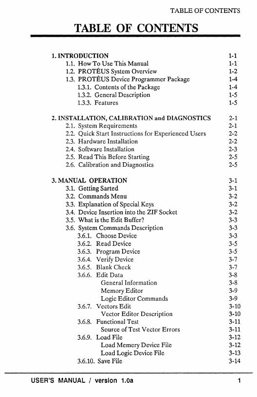
TABLE OF CONTENTS
TABLE OF CONTENTS
1. INTRODUCTION 1-1 1.1. How To Use This Manual 1-1 1.2. PROTEUS System Overview 1-2 1.3. PROTEUS Device Programmer Package 1-4
1.3.1. Contents of the Package 1-4 1.3.2. General Description 1-5 1.3.3. Features 1-5
2. INSTALLATION, CALIBRATION and DIAGNOSTICS 2-1 2.1. System Requirements 2-1 2.2. Quick Start Instructions for Experienced Users 2-2 2.3. Hardware Installation 2-2 2.4. Software Installation 2-3 2.5. Read This Before Starting 2-5 2.6. Calibration and Diagnostics 2-5
3. MANUAL OPERATION 3-1 3.1. Getting Sarted 3-1 3.2. Commands Menu 3-2 3.3. Explanation of Special Keys 3-2 3.4. Device Insertion into the ZIF Socket 3-2 3.5. What is the Edit Buffer? 3-3 3.6. System Commands Description 3-3
3.6.1. Choose Device 3-3 3.6.2. Read Device 3-5 3.6.3. Program Device 3-5 3.6.4. Verify Device 3-7 3.6.5. Blank Check 3-7 3.6.6. Edit Data 3-8
General Information 3-8 Memory Editor 3-9 Logic Editor Commands 3-9
3.6.7. Vectors Edit 3-10 Vector Editor Description 3-10
3.6.8. Functional Test 3-11 Source of Test Vector Errors 3-11
3.6.9. Load File 3-12 Load Memery Device File 3-12 Load Logic Device File 3-13
3.6.10. Save File 3-14
USER'S MANUAL / version 1.0a 1
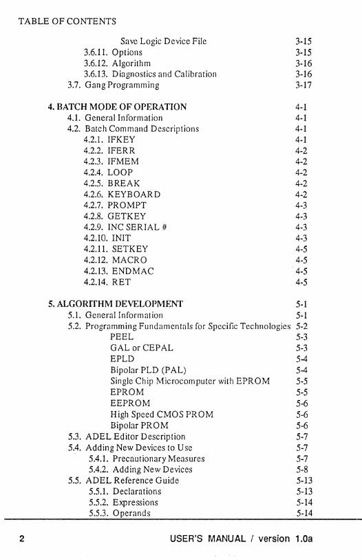
TABLE OF CONTENTS
2
Save Logic Device File 3.6.11. Options 3.6.12. Algorithm 3.6.13. Diagnostics and Calibration
3.7. Gang Programming
4. BATCH MODE OF OPERATION 4.1. General Information 4.2. Batch Command Descriptions
4.2.1. IFKEY 4.2.2. IFERR 4.2.3. IFMEM 4.2.4. LOOP 4.2.5. BREAK 4.2.6. KEYBOARD 4.2.7. PROMPT 4.2.8. GETKEY 4.2.9. INC SERIAL #
4.2.10. INIT 4.2.11. SETKEY 4.2.12. MACRO 4.2.13. ENDMAC 4.2.14. RET
5. ALGORITHM DEVELOPMENT 5.1. General Information
3·15 3·15 3·16 3-16 3-17
4·1 4-1 4·1 4-1 4-2 4·2 4-2 4·2 4·2 4·3 4-3 4-3 4·3 4·5 4·5 4·5 4·5
5·1 5·1
5.2. Programming Fundamentals for Specific Technologies 5-2 PEEL 5~
GAL or CEPAL 5~
EPLD 54 Bipolar PLD (PAL) 54 Single Chip Microcomputer with EPROM 5-5 EPROM 5-5 EEPROM 5-6 High Speed CMOS PROM 5-6 Bipolar PROM 5-6
5.3. ADEL Editor Description 5·7 5.4. Adding New Devices to Use 5·7
5.4.1. Precautionary Measures 5-7 5.4.2. Adding New Devices 5-8
5.5. ADEL Reference Guide 5·13 5.5.1. Declarations 5-13 5.5.2. Expressions 5·14 5.5.3. Operands 5-14
USER'S MANUAL I version 1.0a

TABLE OF CONTENTS
5.5.4. Constants and Modifiers 5·14 5.5.5. Identifiers 5·15 5.5.6. Strings 5·16 5.5.7. Function Calls 5·16 5.5.8. Operators 5·16
Assignment Operators 5·16 Binary Operators 5·17 Unary Operators 5·17
5.6. Directives 5-17 5.6.1. # hvtable 5-17 5.6.2. # load 5-18 5.6.3. # pin 5-18 5.6.4. # ttltable 5-19 5.6.5. # vectors 5·19
5.7. Device Map Directives 5·20 5.7.1. # base 5-20 5.7.2. !count 5-20 5.7.3. Device Record Format 5-21 5.7.4. %elementID 5-21 5.7.5. + incafter 5-21 5.7.6. > resetafter 5-21 5.7.7. " restafter 5·21
5.8. Commands 5-22 5.8.1. aput 5-22 5.8.2. charge 5·22 5.8.3. cset 5-23 5.8.4. delay 5·23 5.8.5. get 5·23 5.8.6. getvoltage 5-24 5.8.7. iput 5-24 5.8.8. Iget 5-25 5.8.9. put 5-25 5.8.10. putentry 5·25 5.8.11. grpset 5-26 5.8.12. rsput 5·26 5.8.13. rsputentry 5-26 5.8.14. set 5-27 5.8.15. sget 5·27 5.8.16. slope 5·28 5.8.17. sput 5·28 5.8.18. sputentry 5-28 5.8.19. test 5·29
5.9. Statements 5-29 5.9.1. break 5·29
USER'S MANUAL I version 1.0a 3
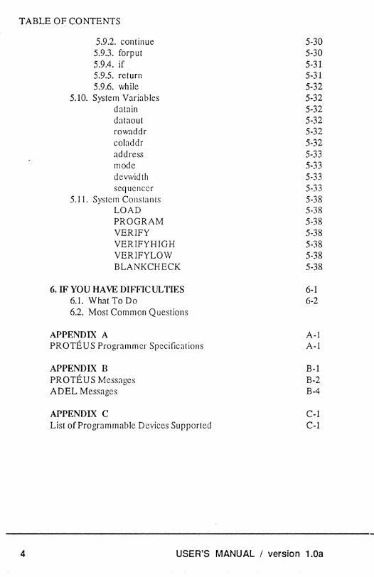
TABLE OF CONTENTS
5.9.2. continue 5.9.3. forput 5.9.4. if 5.9.5. return 5.9.6. while
5.10. System Variables datain dataout rowaddr coladdr address mode devwidth sequencer
5.11. System Constants LOAD PROGRAM VERIFY VERIFYHIGH VERIFYLOW BLANK CHECK
6. IF YOU HAVE DIFFICULTIES 6.1. What To Do 6.2. Most Common Questions
APPENDIX A PROTEUS Programmer Specifications
APPENDIX B PROTEUS Messages ADEL Messages
APPENDIX C List of Programmable Devices Supported
5-30 5-30 5-31 5-31 5-32 5-32 5-32 5-32 5-32 5-32 5-33 5-33 5-33 5-33 5-38 5-38 5-38 5-38 5-38 5-38 5-38
6-1 6-2
A-I A-I
B-1 B-2 B-4
C-l Col
4 USER'S MANUAL I version LOa

INTRODUCTION
1. INTRODUCfION
Welcome to the PROTEUS System and the PROTEUS Universal Device Programmer.
We are confident that you will find PROTEUS to be a reliable, good quality and easy to use instrument which combines professional quality with user effortless software upgradeability based on ADEL (Algorithm DEvelopment Language).
1.1. How To Use This Manual
Although called a User's Manual, this document is also a Reference Guide and contains all the information required to operate the PROTEUS Programmer. It includes Operation instructions, usually found in User's Manuals, as well as a complete Programmer Commands and ADEL (Algorithm DEvelopment Language) Reference Guide.
Most people do not read User's Manuals cover-to-cover before using a software program or operating a new instrument. As a matter of fact users will open a User's Manual only as a last resort and typically to find the answer to a specific question or problem.
The emphasis of this manual is focused on offering effective, easilyaccessible information usefull for operating the Proteus Programmer.
As a general rule, examining the table of contents will tell you where to find information related to your immediate area of interest. The following paragraphs will explain where to find pertinent information related to some of the most common operations that you might want to perform.
Note: Before operating the PROTEUS Programmer, users are advised to read Chapter 2, "Installation, Calibration and Diagnostics" entirely, or at least Section 2.2, "Quick Start Instruclons for Experienced Users" and Section 2.5 "Read This Before Starting". Doing so will reduce the chances of damaging the Programmer or device to be programmed.
USER'S MANUAL I version 1.0a 1-1
INTRODUCfION
To fmd out generalities about the PROTEUS System, read Section1.2, "Proteus System Overview". As you probably know by now, the PROTEUS Programmer is only one application on the PROTEUS Main Unit. You will find out more on the other applications in this section.
An overview of the PROTEUS Programmer Package is given in Section1.3, "Proteus Device Programmer".
If you want to learn more about operating the programmer after installation, you should read Chapter 3, "Programmer Operation". Section 3.1.3, "Common Command Sequences" will help you execute most of the basic operations related to programming devices. The remainder of Section 3.1 describes in detail the System Commands.
The Batch Mode of operation is described in Section 3.2, "Batch Mode of Operation". This section is for advanced users who might want to write user macros in order to make certain repetitive operations more efficient to execute. It is also useful when interfacing the PROTEUS with a Device Handler.
Users in need to add their own devices to the User Device Library will need to read Chapter 4, "Algorithm Development".
In case of difficulty when starting PROTEUS or if any errors are encountered, read Chapter 5, "If You Have Difficulties".
Appendix A, Band C contain the PROTEUS Programmer Specifications, the Supported Device List and System Error Messages.
1.2. PROTEUS System Overview
1-2
PROTEUS is a multifunctional device which has the ability to be configured as a Universal Device Programmer, Universal PCB or Device Tester, Data Logger, Controller or Programmable Power Supply.
PROTEUS can be operated in stand-alone mode by means of the optional removable and portable PROTEUS PC which is IBM-XT compatible. It can also be operated in computer link mode connected to the parallel printer port of any IBM-PC/XT/AT/386 or PS/2 type computer via a standard parallel printer port cable.
USER'S MANUAL / version 1.0a
INTRODUCTION
The advent of Personal Computers brought engineers and scientists inexpensive PC based instrumentation and development tools. Most commonly, regular IBM-PCs or compatibles are outfitted with specific add-on boards in order to be capable of performing a variety of special functions (i.e. Data Acquisition, Industrial Control, Device Programming) or are linked via a custom parallel interface plug-in card to an external box performing a specific hardware related task (i.e. Universal Device Programmers, Data Loggers, Input/Output devices).
Thanks to its built-in standard PC parallel printer port interface, PROTEUS can offer many of the functions performed by this type of equipment without the inconvenience of inserting a custom plug-in card into your PC, or the inflexibility of assigning a specific computer to perform a dedicated hardware function.
PROTEUS Hardware: The PROTEUS Main Unit contains the control logic and pin driver electronics for up to 104 fully analog & digital input-output pin drivers/receivers. It also houses a fully protected power supply and interfacing port for PC communications. The Main Unit accepts a variety of Adapter Modules: Gang/Set Programmer Adapter Module for E(E)Proms, Microcontrollers and Memory Cards (PCMCIA/JEIDA) , PLCC Programmer Adapter Module, Tester, Data Logger, Controller and Programmable Power Supply Adapter Module.
The modular design allows for straightforward upgrading, via internal modules, from the basic configuration of 4D to 104 pin drivers/receivers. For applications that require a greater number of pins/channels, (e.g. programming programmable gate arrays, testing PCBs with more than 104 testpoints, data logging hundreds of channels), the basic 40 pin driver configuration can be also upgraded via external adapter modules to a total of 296 pin drivers. In fact, for applications that are not speed critical, the pin driver expansion capability is practically limitless. This is due to the fact that the Adapter Modules interface to the main unit via the PROTEUS BUS, which makes all the important system signals available for external interfacing. The internal pin drivers/receivers have analog and digital capabilities with specifications listed below.
PROTEUS Software: The PROTEUS software is centered on ADEL, a proprietary Algorithm Development Language offered with its own development environment embedding a fully integrated editor and compiler. ADEL is a high level language, which was specifically designed to allow efficient
USER'S MANUAL / version 1.0a 1-3

INTRODUCTION
and effortless development of application programs. All Application Programs for PROTEUS consist of a core program and a user customizable/maintainable library written entirely using ADEL. Since ADEL is embedded in the core program, all libraries can be modified on-the-fly, thus allowing users effortless program customizationlmaintainance .
. . l11~;;t~erigtl1 ~i· .,ROTE(jS.,~"$ mUltif~n~tionality,. which ·is •. achiev~~by ComiJining:the.:PROTEIJ$. rrul,n~"'itaridits as~
/ ~ociaf~~ ::~d~pier~:wlthth~power ~hldflexi6jJity·ofADEL.· (Al~ .. gorithIT(ilE'f~lopmeiitLanguage)~.the ;:erid·re~u.lf :b.eilig.8 . Very ..
.• :. POV(~~~I;'~ef$a.tite;easy .·to: use and ... cost~eftectlvein$trulllert ..
1.3. PROTEUS Device Programmer Package
1-4
1.3.1. Contents of the Package
The basic PROTEUS Programmer package consists of four items: - PROTEUS Main Unit with 40 pin drivers capability - 40 pin DIP ZIF Programming Adapter Module - Parallel Printer Port Cable - PROTEUS Programmer System Software - PROTEUS User's Manual
In addition to this you may have received the following options: - ADEL (Algorithm Development Language): For a limited time, ADEL will be included in the basic PROTEUS Programmer. This option is in fact a built-in, fully integrated feature of the PROTEUS Programmer System Software. You will know if you received ADEL by examining the Main Program Menu and verifying whether the last item listed is ADEL. - PROTEUS-PC (including a SI2K RAM card and a PROTEUS-Link cable for communicating with regular PCs via the serial port)
Note: If any of the above listed items are missing, contact B&C Microsystems Immediately.
USER'S MANUAL I version 1.0a

INTRODUCTION
1.3.2. General Description
The PROTEUS Programmer is a low cost, high quality Universal Programmer capable or programming most Memory as well as Logic Devices. The list of supported programmable devices is given in AppendixC.
PROTEUS can be connected to any PC with a standard parallel port, or can be used in stand-alone mode with the optional PROTEUS-PC computer.
In it's standard configuration, the PROTEUS Programmer can support devices with up to 4{) pins. The pin drivers can be expanded internally to support devices with up to 104 pins.
The PROTEUS Programmer Specification can be found in Appendix A.
1.3.3. Features
The PROTEUS Programmer contains a series of hardware as well as software features not found in most, and in some cases any universal programmers on the market today. The most noteworthy of these features are presented in the following:
Algorithm Development System: No other programmer on the market offers a custom language and fully integrated environment for adding parts to the device libraries, to the extent that the language editor and compiler is actually part of the Programmer System Software. This feature allows for a significantly faster device library update cycle. At the same time, users will be able, using ADEL, to add new parts themselves or to modify algorithms, parameters and pincodes for existing devices.
Batch Mode Of Operation Based On A Macro Language: Most lowend programmers do not support batch mode. Even higher-end programmers have limited batch features, most of them only allowing the user to record keystrokes in a batch file. PROTEUS provides powerful macro language supporting features such as: IF THEN ELSE structures, LOOPs and User Interface Commands.
On-Board I In-Circuit Programming: This capability is found most commonly in either custom or high-end programmers and allows users
USER'S MANUAL I version 1.0a 1-5

INTRODUCTION
1-6
to program devices without removing them from their Printed Circuit Board. Thanks to the Symbolic Pinout Mapping employed in PROTEUS and with the help of ADEL, writing custom programs to perform On-Board Programming and interfacing to the user's target system is extremely easy to accomplish.
Hardware Expandability: The main unit can accomodate virtually any type of dedicated adapter module. The entire PROTEUS BUS, containing all relevant system signals, is accessible to any plug-in adapter module via four 50 pin connectors.
State Machine Testing: PROTEUS has the capability of clocking all pins simultaneously, thus allowing for true state-machine testing. As a general rule, low-end programmers set the logic levels on individual device pins sequentially and therefore can perform only limited functional testing on logic devices.
Fast Risetime Eliminates Double Clocking Errors: Most universal programmers have slow rise times (over 5 f.Ls) when driving logic in puts. Although this is fine in most cases during the programming process of a device, it often causes Double Clocking Errors while performing functional testing. PROTEUS employs high speed pin drivers that have rise times of less than lOOnS, thereby eliminating problems of this type.
Register and Buried Register Preload: Since the register preload sequence is different for each device, most programmers which do support this feature do so only for standard devices. Adding or modifying a specific device algorithm to support the register preload feature can be performed, even by the user, within minutes.
Correct Device Insertion Detection: Before attempting to perform an operation on a device, PROTEUS verifies whether or not the device is defective. In addition to this, PROTEUS can determine whether the device inserted in the ZIP socket is reversed (upside-down insertion) and even if pin no.1 is not aligned properly (shifted insertion). By means of this capability, PROTEUS can be configured to operate in an Autostart Mode, in which the device insertion in the ZIP socket is detected, verified for correctness, and the programming / verify process initiated without further operator prompting.
Support For New Devices: Unlike most low-end programmers, the PROTEUS hardware has no inherent limitations related to programming any particular type of device. PROTEUS can even handle devices that require programmable current limiting during fuse burning. The
USER'S MANUAL I version 1.0a
INTRODUCTION
current device list supports over 1000 parts from all major programmable device manufacturers. Due to ADEL, the device library will be expanded rapidly. Virtually all new devices on the market, as well as future devices, will be added to our device library in a shorter time frame than most if not all other programmer manufacturers.
Additional Features:
• Friendly, menu-driven User Interface; Device selection by manufac turer, part number and string search
• Built-in full screen Memory, Fuse Map and Test Editor • Reads 1MB EProms in 10 seconds • Programs 1MB EProms in 35 seconds • GANG, SET, SPLIT programming capability • Selectable wordsizes; Supports most file formats • Program-selectable decoupling capacitors and Clock Sources
(4MHz) • Gold plated Textool ZIF socket • Interface for Device Handlers
USER'S MANUAL / version 1.0a 1-7

INTRODUCTION
This page left intentionally blank.
1-8 USER'S MANUAL / version 1.0a

INSTALLATION, CALIBRATION AND DIAGNOSTICS
2. INSTALLATION, CALIBRATION AND DIAGNOSTICS
Note: Before installing PROTEUS, fill out the Registration Card enclosed in your manual. Make a copy of it and fax or mail it to B&C Microsystems. Customer Support and Software Upgrades will not be provided until the completed Registration Card has been received.
2.1. System Requirements
In order to install the PROTEUS hardware and software you will need the following:
IBM-PC/XT/AT/386 or compatible computer (unless you have ordered the PROTEUS-PC)
Monochrome, CGA, EGA or VGA monitor
Minimum 512KB RAM
Parallel printer port (LPTl or LPT2)
Floppy disk drive for loading the PROTEUS Software Formats supported: 360KB, nOKE, 1.2MB, 1.44MB
Optional hard disk drive is recommended to take full advantage of the speed of PROTEUS. A hard disk is required to run the PROTEUS soft ware on PCs with floppy drives of capacity smaller than nOKB.
Note: Before installing the software on your hard disk make sure you have at least 700KB of disk space available.
USER'S MANUAL / version 1.0a 2-1

INSTALLATION, CALIBRATION AND DIAGNOSTICS
2.2. Quick Start Instructions for Experienced Users
• Connect PROTEUS to your computer by plugging the Printer Cable provided with the unit into your available Parallel Printer Port. (PROTEUS will detect automatically which port you are using.)
• Make sure that the 1l0/220V AC switch, located on the back panel next to the power switch, is set correctly and verify that the Adapter Module installed in the main unit is plugged in properly.
• Plug the included power cord into PROTEUS and then into an AC outlet.
• Install the PROTEUS software by inserting the program diskette into drive A: and then typing:
A: INSTALL [D:]
where D: is the drive onto which you want to install the software (default drive is C:).
• Turn the power switch, located on the back panel of PROTEUS, to ON. Check if the red LED located at the Adapter Module and labeled "POWER" is ON.
• Run the PROTEUS Programmer software by typing:
PROTEUS [ENTER]
If for any reason your computer cannot communicate with PROTEUS, the program will automatically configure itself as a DEMO program and you will notice "PROTEUS Driver 1.x (DEMO mode)" at the top of the screen.
If this is not the case and if PROTEUS completes successfully the autodiagostics and calibration, you will be ready to use the PROTEUS Programmer. The entire start-up process can take from 10 to 60 seconds, depending on the speed of your computer.
2.3. Hardware Installation
2-2
There are two cables provided with PROTEUS: a Parallel Printer Cable and an AC Power Cable.
USER'S MANUAL I version 1.0a

INSTALLATION, CALIBRATION AND DIAGNOSTICS
Before connecting any of the cables be sure that the 110/220V AC switch, located on the back panel next to the power switch, is set to the appropriate AC voltage and verify that the Power Switch is set to OFF (depressed in the lower position). Inspect also the Adapter Module mounted on top of the main unit to insure that it is plugged-in correctly.
Plug the included Power Cord into PROTEUS and then into an AC outlet.
Connecting PROTEUS to your PC is as simple as connecting a Parallel Printer. No special interface cards are required and any Parallel Printer Port can be used (LPTl-4). A Parallel Printer Cable is provided for this purpose. Although you might already have a Parallel Printer cable connecting your computer with your printer, you should use the cable provided with PROTEUS to connect the programmer. Any Parallel Port can be used without the need for switch settings on the hardware side, or software configuration parameters on the software side. The PROTEUS Programmer Software will automatically detect to what port you have connected PROTEUs.
2.4. Software Installation
The PROTEUS Programmer System Software is provided on one 360KB diskette containing the following files:
README.TXT
INSTALL.EXE
(Contains last minute information not included in the manual) (Installation Program) Install.dat (Data file used by the Installation Program)
Make a backup copy of the PROTEUS software diskette and store the original in a safe place.
In order to install the PROTEUS Programmer System Software you need to insert the program diskette in drive A: and then type:
A:INSTALL [D:]
where D: is the drive on which you want to install the software (default drive is C:). A directory called "PROTEUS" will be created The system
USER'S MANUAL / version 1.0a 2-3
INSTALLATION, CALIBRATION AND DIAGNOSTICS
2-4
fIles will then be extracted from the fIle Install.dat and copied to the directory "PROTEUS". You will be able to monitor the entire process on the screen. The following message will be an indication that the installation was performed without problems:
PROTEUS Programmer System Software installed successfully!
After a successful installation you will have the following files in the PROTEUS subdirectory:
PROTEUS.BUF PROTEUS.HLP PROTEUS.MAC PROTEUS.IDX SYS.DEV SYS.DMP SYS.FAM SYS.IDS SYS.PIN SYS.TAB SYS.ALG USER.DEV USER.DMP USER.DSO USER.FAM USER.FSO USER.IDS USER.PIN USERPSO USERTAB USER.TSO USER.ALG USERASO
You can now type:
PROTEUS < ENTER>
to start the program.
If the message "PROTEUS Ready!" does not appear, follow the instructions given in Chapter 6, "IF YOU HA VB DIFFICULTIES".
USER'S MANUAL I version 1.0a

INSTALLATION, CALIBRATION AND DIAGNOSTICS
Turn ON the Power Switch located on the back panel. Check if the red LED (Light Emitting Diode) located on the Adapter Module and labeled "POWER" is ON. If this is not the case go to Chapter 6, "IF YOU HA VB DIFFICULTIES".
2.5. Read This Before Starting
Before turning ON the Power Switch on PROTEUS, make sure that the 110/220 V AC switch, located on the back panel next to the Power Switch, is set correctly and verify that the Adapter Module installed in the main unit is plugged in properly.
After starting the PROTEUS Programmer Program, wait until you see the message:
PROTEUS READY.
DO NOT INSERT the device to be programmed in the socket until PROTEUS passes auto diagnostics and calibration. Failing to do so will most likely damage the device you want to program due to the fact that the autodiagnostic and calibration process will set all the ZIF pins to voltages ranging from OV to 25.6V
You are now ready to use the PROTEUS Programmer.
For operation instructions, see Chapter 3, "MANUAL OPERATION".
2.6. Calibration and Diagnostics
The calibration and diagnostics are done automatically upon starting the PROTEUS program if the PROTEUS programmer is detected as being connected to the parallel port and if it initializes correctly.
There is no adjustment or manual calibration that the user will have to perform. During Calibration and Diagnostics, the program detects the present pin configuration and steps all the pins from OV to 25.6V in increments of 25mV. For this reason, it is very likely that, if a device is present in the ZIF socket, it will get damaged. The Calibration and
USER'S MANUAL I version 1.0a 2-5
INSTALLATION, CALIBRATION AND DIAGNOSTICS
Diagnostics process will not start, however, if a device is detected in the ZIP socket beforehand.
If the calibration and diagnostics is completed successfully, you will see the following message on the screen:
PROTEUS READY!
USER'S MANUAL / version 1.0a
MANUAL OPERATION
3. MANUAL OPERATION
PROTEUS can be operated manually or in batch mode. Manualoperation is typically used in a non-production environment while batch mode of operation is implemented for production optimization.
This chapter describes the manual mode of operation and details all System Commands.
3.1. Getting Started
In order to start using PROTEUS, turn ON the Power Switch on the programmer. Then go to the Proteus subdirectory, in case you are not already there, and type:
Proteus < Enter>
You will notice a Header Window appearing on your screen, in which you will be able to read the program Version Number, the currently (or last) selected device and the device checksum.
During system initializaion you will notice a series of short flashing messages appearing in this window, informing you about the steps the program is performing. If the programmer passes successfully auto calibration and diagnostics, the last message you will see in this window will be:
PROTEUS Ready!
Then, two more windows will appear on your screen: the MAIN MENU and the OPTIONS window.
You will always have a default device being selected, even when you first install and run the software. The default device is the device that was selected before you last exited the program. The first step to take will probably be to select a new device from the device library. The selected device will be remembered for the next programming session after you exit the program.
USER'S MANUAL / version 1.0a 3-1

MANUAL OPERATION
3.2. Commands Menu
The Commands menu will let you select the operation to be performed. The selection can be performed using the Arrow keys (Up and Down), or by typing the first letter of the command to highlight the selection, and then by pressing < Enter> or the < Space> bar.
The commands are organized in an intuitive order and have selfexplanatory designations. With the exception of the Options Menu selection, all of the other selections will display on the screen an associated window which will enable you to perform the selected operation.
The Options menu selection will allow the modifications of the Options parameters in the Options window.
Section 3.6. describes all the system commands in detail.
3.3. Explanation of Special Keys
At the bottom of the Main Screen you will find a line showing the function of special keys used throughout the program. They are:
Fl: <SPACE> or <Enter> : F9:
FlO: ESC:
Brings up the Help file.
Executes the menu selection; temporarily suspends. Suspends temporarily operation and jumps to DOS. (From DOS type "EXIT" to return to program.) Enables Command line operation. Prompts for confirmation and then exits to DOS.
3.4. Device Insertion into the ZIF Socket
3-2
The Proteus programmer has the capability to detect the presence of a device in the ZIF (Zero Force Insertion) socket and even to determine if the device is inserted correctly. Before any operation is executed that applies voltage to the device, the connection of the device to the socket is first tested. A backwards or offset device insertion will cause an
USER'S MANUAL I version 1.0a

MANUAL OPERATION
error message, as will a device inserted with a bent or broken pin. The detection of a device in the socket with more than the expected number of pins will also cause an error.
Should Proteus report such a Continuity Error, the user will have the option to abort or continue the operation.
3.5. What is the Edit Buffer?
Before reading about all the system commands it is useful to understand the basic principle of operation of the programmer.
The edit buffer (or data buffer) is a memory space that is used to store data temporarily. The data can come from a device which you might want to read, or it can come from a diskfile containing for example, microprocessor executable code generated by an assembler program.
Once loaded in the the Edit Buffer, this data can be modifed and used to program a device or it can be just rewritten, possibly in a different format, back to the disk.
Being that the data transfer to and from a device is always performed in binary form, there are no options to select from the OPTIONS menu related to the data transfer.
On the other hand, Loading or Saving data from and to a disk will require a file name as well as a file format selection. You will read more about this in the following section.
3.6. System Commands Description
The following are descriptions of the PROTEUS System Commands.
3.6.1. Choose Device
This is the first selection in the Commands Menu. Use the Arrow keys to highlight this selection and hit the < SPACE> bar or the < Enter>
USER'S MANUAL / version 1.0a 3-3
MANUAL OPERATION
3-4
key. A manufacturers list will appear on the screen. You will need to enter in the blinking window the two digit number corresponding to the device manufacturer you want to select. Doing so will highlight the manufacturer selected.
Before hitting < Enter> or < Space> verify that the Device Family field highlighted to the right of the blinking field, where you entered the manufacturers selection code, is the desired one. The device families listed are:
All: Displays all the devices for all the device families for the se-lected device manufacturer.
Logic: Displays the Logic devices for the selected manufacturer. Memory: Displays Memory devices for the selected manufacturer. Micros: Displays the Single Chip Microcomputer devices for the
selected manufacturer. Test les: Displays the Logic or Memory Devices to be tested for the
selected manufacturer. Other: Displays other type of programmable devices from the se
lected manufacturer.
Every Device Family field has a highlighted letter. Typing that letter at any time during the selection of the device manufacturer will select the desired device family.
After pressing < Enter> or < Space> you will see on the screen a list of devices from the selected manufacturer, all being of the family selected.
You will be able to select the device by using the Arrow Keys or by typing the device ID number in the blinking field, followed by the < Enter> or < Space> key. If the device list extends past the size of one screen, use the <PgUp>, <PgDn>, <End> and <Home> keys.
After selecting the desired device, the program will load the specific algorithms for the selected device into memory, will set-up the appropriate option selections in the OPTIONS window and will configure the edit buffer according to the family and size of the selected device. The programmer will then return to the Function Menu.
Pressing the < ESC > key at any time during the device selection process will abort the current operation and return you to the previous screen.
USER'S MANUAL I version 1.0a
MANUAL OPERATION
3.6.2. Read Device
Selecting this function reads the data from the device inserted in the ZIF socket and copies it into the edit buffer. The address range for the reading operation, can be set using the OPTIONS Menu selection described in Section 3.6.11, the default range being the size of the device.
A checksum is automatically performed on the data and displayed in the right upper corner of the screen, unless it is you disable the checksum generation from the OPTIONS Menu.
During the reading operation you will see on the screen the message:
Read In Process
If the operation is successful, at the end of the operation you will see the following message on the screen:
Device Read OK.
The reading process can be followed by a second reading for verification purposes. This is an option which can be set in from the OPTIONS Menu. You can find out more about this feature in Section 3.6.11.
Pressing the < ESC > key at any time during the reading process will abort the command and return you to the Commands Menu.
Note: 00 not remove the device to be read from the ZIF socket during the reading process. Doing so might damage the device.
3.6.3. Program Device
This command performs the reverse of the Read Device command. It takes the data in the edit buffer and programs it into the device placed in the ZIF socket. Similar to the Reading function, the address range for the programming operation can be set using the OPTIONS Menu selection, the default range being the size of the device.
During the reading operation you will see on the screen the message:
USER'S MANUAL / version 1.0a 3-5
MANUAL OPERATION
3-6
Program In Process
Before actually programming the device, the programmer will verify if the device is blank (erased). The devices that are electrically erasable or rewritable, such as EEPROMs, will be erased automatically if found not to be blank. If the device is found not to be blank, but cannot be erased or rewritten, then you will receive the following prompt:
Device is not blank. Continue (Y/N)?
If you answer Yes then the data in the device will be overwritten with the new data.
Each device has a specific programming algorithm specified by the manufacturer, which is automatically determined when the part is selected from the device library. Selecting a different algorithm is not an option unless you want to program a part from the USER Library and create or modify, yourself, the programming parameters.
Each memory cell is verified after being programmed. If an error occurs, the process will be immediately aborted and an error message will be displayed.
Additional verify cycles could be performed if specified in the OPTIONS Menu. Read more about this feature in Section 3.6.11.
Some devices have a built-in protection that prevents the device from being read after being programmed. This is typically implemented using a Security Fuse that can be programmed at the end of the programming cyle. After programming the Security Fuse the data inside the device can no longer be accessed. If the device is supporting this feature, the OPTION menu will let you set the option to blow the Security Fuse after programming.
If the operation is successful, at the end of the operation you will see the following message on the screen:
Device Programmed OK.
Pressing the < ESC > key at any time during the reading process will abort the command and return you to the Function Menu.
USER'S MANUAL I version 1.0a
MANUAL OPERATION
Note: Do not remove the device to be programmed from the ZIF socket during the reading process. Doing so may damage the device.
3.6.4. Verify Device
Selecting this function verifies the data from the edit buffer against the device inserted in the ZIF socket. The address range for the verify operation can be set using the OPTIONS Menu selection described in Section 3.6.11, the default range being the size of the device.
During the reading operation you will see on the screen the message:
Verify In Process
If the operation is successful, at the end of the operation you will see the following message on the screen:
Device Verified OK.
If a problem is encountered during the verify process, an error message will be displayed on your screen and the operation will be aborted.
Pressing the < ESC> key at any time during the verifying process will abort the command and return you to the Function Menu.
Note: Do not remove the device to be verified from the ZIF socket during the verifying process. DOing so may
damage the device.
3.6.5. Blank Check
This function checks whether the device inserted in the ZIF socket is blank (erased). The address range for this operation can also be set using the OPTIONS menu selection described in Section 3.6.11, the default range being the size of the device.
During the operation you will see on the screen the message:
USER'S MANUAL / version 1.0a 3-7
MANUAL OPERATION
3-8
Blankcbecldng Device
If the operation is successful, at the end of the operation you will see the following message on the screen:
Device Blankchecked OK.
If a problem is encountered during the blankcheck process, an error message will be displayed on your screen and the operation will be aborted.
Some devices will always fail the blankcheck operation due to the fact that they have no stable unprogrammed state. In such a case, the state of the cells is unpredictable and this test will most likely fail.
Pressing the < ESC> key at any time during the blankcheck process will abort the command and return you to the Function Menu.
Note: Do not remove the device to be blankchecked from the ZIF socket during the blankcheck process. Doing so may damage the device.
3.6.6. Edit Data
General Information
As mentioned in Section 3.6, data is not directly transferred between a device and the hard (of floppy) disk. The data is first loaded into the Edit Buffer. Selecting this function from the menu will allow you to modify or create data to be either programmed into a deviced or saved to disk.
Upon selecting a device from the device library, the software is automatically setting up the Edit Buffer. There are two Editor Buffer configurations: Memory Editor and Logic Editor.
The following keys are common in functionality to both editors:
LetlArrow/RigbtArrow UpArrow!DownArrow PgUp/PgDn
Moves cursor left/right Moves cursor up/down Displays the previous/next page in buffer
USER'S MANUAL I version 1.0a

HomelEnd
CtrlH ome/CtrlEn d
Memory Editor
MANUAL OPERATION
Moves cursor at the firstllast address on the page moves cursor at the beginning/end of the edit buffer
The Memory Editor is a full screen editor allowing data entry or alteration in both HEX and ASCII. A set of useful functions can be invoked via Function Keys. The following is a list of the function keys and their attached function:
Fl Displays Help information F3 Places the cursor at the desired address F4 Searches for an indicated ASCII string, starting
from the indicated address F5 Fills an indicated address range of the buffer with a
given value (character) F6 Performs 1's complement on an indicated range of
the edit buffer F7 Copies data from a given range in the buffer to gi
ven address F8 Computes the checksum within a given range of the
memory
Logic Editor Commands
The Logic Editor is a full screen editor customized for fusemap editing. Data entered can only be "-" (fuse blown) and "X" (fuse intact).
The following is a list of the function keys that have specific functions attached to them for Fusemap editing.
Fl Displays Help information F3 Places the cursor at the desired address FS Fills an indicated address range of the buffer with a
given value (character) FlO Allows temporary exiting to DOS CtrlLeft/CtrlRight Shifts the fusemap screen left/right
USER'S MANUAL / version 1.0a 3-9

MANUAL OPERATION
3.6.7. Vectors Edit
3-10
Selecting this function from the Commands menu will bring up the Test Vector Editor screen. Functional Test vectors can be edited with this editor and then used by the Functional Test selection from the Command menu to test if a progammed logic device operates correctly.
Logic design packages like ABEL, CUPL, P ALASM or AMAZE produce as an output of their compilers a me in JEDEC format. This fUe contains the device fusemap and, optionally, a set of test vectors. When loading a JEDEC fUe, if any Test Vectors are detected in the fUe, they are loaded in the Vector Edit Buffer.
The size and format of the Test Vector Editor buffer is dependent on the size of the device selected with the Choose Device command. The buffer has a number of columns equal to the device pin number. Each row in the buffer holds a test vector containing a valid test condition. The following test confitions are supported:
o Set Input Low 1 Set Input High B Buried register preload C Set Input (low, high, low) F Float Input/Output pin H Test output high K Set Input (high, low, high) L Test Output low N Pins not tested (Power, Outputs) P Preload registers X Input don't care (default), Output not tested Z Test Input/Output for high impedence
Vector Editor Description
The Vector Editor has similar features with the Logic Editor. The following Special Keys can be used while inside the Vector Editor.
F3 LeftArrow/RightArrow UpArrow/DownArrow PgUp/PgDn
HomelEnd
Place the cursor to a given vector Previous pin / next pin Previous vector / next vector Displays the previous / next page in buffer Places cursor at the beginning / end of page
USER'S MANUAL / version 1.0a

CtrIHomelCtrlEnd
3.S.S. Functional Test
MANUAL OPERATION
places cursor at the beginning / end of buffer
This command is used to test a programmed logic device against a set of predefined test vectors. Selecting this command will apply the test vectors found in the Test Edit buffer to the device in the ZIP socket.
In case the device will pass the functional test you will see the following message on the screen:
Device Passed Functional Test!
If an error occurs, a message will appear on the screen indicating the failing vector and pin number.
The functional test is performed in the following manner:
Pass1 - The input pins are set to levels 0, 1, X according to the test vector - The output pins are all set to Read Mode. - If any P or B vectors are found, they will be executed in this pass. Pass2 - Applies the clock pulses, if they are found, to the respective pins. Unlike most programmers, Proteus can apply multiple clocks simultaneously. Pass3 - Checks the output of the device against the test vectors
The cycle is repeated until all the test vectors are exhausted or until an error occurs.
Sources of Test Vector Errors
Preload: The preload feature found in the more advanced PLDs is one of the most difficult to support. Preload sequences differ not only from device to device, but sometimes also between two manufacturers of an equivalent part.
There are situations when a pin used for asynchronous reset might be used also in the preload sequence. This will automatically undermine
USER'S MANUAL / version 1.0a 3-11
MANUAL OPERATION
the preload operation. The built-in Vector Editor is very helpful when dealing with problems of this nature. Changes to test vectors can be made immediately and the development time shortened significantly.
Power-On Reset: It happens sometimes that the Functional Test fails after the first vector. This is often caused by the the fact that the Power-On condition is not defmed in the first test vector. In order to correct such a problem, an initialization test vector might have to be added as the first vector. This vector will then reset the internal registers and put them in and in a stable state.
Signal Sequence: Unlike most universal programmers which apply functional test levels sequentially, PROTEUS has the capability to apply all signals to the pins simultaneously. This eliminates errors caused by sequencing of the test signals to the device pins during testing.
Asynchronous or Multiple Clocks: Unlike most universal programmers, PROTEUS can perform simultaneous clocking, thus eliminating asynchronous and multiple clock errors.
Synchronous Clocks: Since PROTEUS applies all logic levels simultaneously and pin risetimes are less than lOOns, all synchronous clock errors are eliminated.
3.6.9. Load File
3-12
Load Memory Device File
Selecting this function loads the data from the file specified in the Load File window and copies it into the edit buffer. The Load File operation requires the following parameters:
Filename - The fllename is the first paramter to be specified in the Load File window. If you enter a filespec containing wildcard characters, the appropriate flle listing will appear in the Load File window.
From address· Specifies the beginning address of the edit buffer to load data from.
USER'S MANUAL / version 1.0a
MANUAL OPERATION
To address· Specifies the beginning address of the edit buffer to load data to.
Block size· Specifies the number of the bytes to load into the edit buffer.
Current set· Specifies the current virtual device section of the edit buffer to be loaded.
From byte [##] of [##] • Specifies which byte of the byte group to be loaded from the file. For example: to load all odd addresses one would specify: From byte [2] of [2].
To byte [##] of [##] • Specifies which byte of the byte group to load the file data into.
File Format - Specifies the format of the file to be loaded into the buffer. The supported formats are listed in the LOAD FILE window.
Pressing < Enter> will start the loading process. The following message will be displayed on the screen if there were no errors encountered:
Operation Complete.
The checksum is automatically performed on the data and displayed in the right upper corner of the screen, unless you have disabled the checksum generation from the OPTIONS menu.
Load Logic Device File
Selecting this function while having a logic device selected, loads the data from the file specified in the Load File window and copies it into the edit buffer.
In case of loading a data file into the Logic Edit Buffer for the purpose of programming a PLD (Programmable Logic Device), the file must be in JEDEC format. All PLD software design packages (e.g. PALASM, ABEL, CUPL, or AMAZE) can generate JEDEC files. JEDEC files contain the information required to program a PLD but have the capability to also contain Test Vectors. If Test Vectors are encountered in a JEDEC file while it is loaded, the vectors are stored automatically in the Vector Edit Buffer. This will enable the user to perform Functional Testing.
USER'S MANUAL / version 1.0a 3·13
MANUAL OPERATION
The Load File operation requires the following parameters:
Filename - The mename is the ftrst parameter to be specifted in the Load File window. If you enter a mespec containing wildcard characters, the appropriate me listing is will appear in the Load File window.
Press < Enter> to start executing the Load Device command.
3.6.10. Save File
3-14
Save Memory Device File
Selecting this function saves the data from the Edit buffer into the me specifted in the SAVE FILE window. The Save File operation requires the following parameters:
Filename· The mename is the ftrst paramter to be specified in the Save File window. If you enter a filespec containing wildcard characters, the appropriate file listing is will appear in the Load File window.
From address • Specifies the beginning address of the edit buffer to save data from.
To address· Speciftes the beginning address of the file to save data to.
Block size· Specifies the number of the bytes to save to file.
Current set· Speciftes the current virtual device section of the edit buffer to be saved.
From byte [##] of [##] • Specifies which byte of the byte group to be saved from the edit buffer. For example: to save all odd addresses one would specify: From byte [2] of [2].
To byte [##] of [##] • Speciftes which byte of the byte group to save the edit buffer data into.
File Format - Speciftes the format ofthe file to be save on the disk. The suppoerted formats are listed in the SA VE FILE window.
Pressing < Enter> will start the saving process. The following message will be displayed on the screen if there were no errors encountered:
USER'S MANUAL / version 1.0a
MANUAL OPERATION
Operation Complete.
The checksum is automatically performed on the data and displayed in the right upper corner of the screen, unless you have disabled the checksum generation from the OPTIONS menu.
Save Logic Device File
Just like above, selecting this function while having a logic device selected, saves the data from the Logic Editor Buffer to the file specified in the SA VB FILE Window.
The Save File operation requires the following parameters:
Filename - The filename is the first parameter to be specified in the SA VB File Window. If you enter a filespec containing wildcard characters, the appropriate file listing will appear on the screen.
Press < Enter> to start executing the Save Device command.
3.6.11. Options
Selecting this menu option enables the user to set-up or alter the following programming options.
Library • PROTEUS is offered with two device libraries, SYS and USER. The SYS library contains standard memory and logic devices which are implemented according to manufacturers specifications. If the user wants to alter a device or to add a new device to the library, he needs to select the USER library. The SYS library is read and write protected in order to prevent inadvertent damaging of the programming algorithms, as well as to protect device manufacturers proprietary information.
Blankcheck - Allows the configuration of the programmer to perform a blank check on the device inserted in the ZIF socket before initiating the programming cycle.
Verify. Selecting this option will let the user determine if the programmer should execute an additional verification cycle at the end of the programming cyle, and how to perform this extra cycle. There are three values that can be selected for this option: S, W, N. Selecting S (Standard) performs a verification at nominal vee operating voltage, W
USER'S MANUAL / version 1.0a 3·15
MANUAL OPERATION
(Worse) performs a verification at worst case operating voltages and N (None) disables this feature.
FromAddress - This option is used only when memory devices are selected. It defmes the starting address for loading, programming or verifying operations performed on the selected device.
ToAd dress - This option is also used only when memory devices are selected. It defines the ending address for loading, programming or verifying operations performed on the selected device.
Checksum - This option can be enabled or disabled according to the user. In some instances it is useful to always have the ckecksum computed for any data transfer to and from the Edit Buffer. In others this option can be disabled in order to speed up the switching between the program screens.
Sound ON - Allows the user to switch the programmer sound effects OFF or ON.
3.6.12. Algorithm
Selecting Algorithm from the Command Menu will permit access to ADEL for modifications of programming parameters or additions of new parts. Read Chapter 5, "ALGORITHM DEVELOPMENT" for more information on ADEL.
3.6.13. Diagnostics and Calibration
Selecting this command will execute the autocalibration and diagnostics. If no errors are encountered, the message PROTEUS OK! will be displayed on the screen.
USER'S MANUAL I version 1.0a
MANUAL OPERATION
3.7. Gang Programming
Using the PROTEUS programmer, equipped with a Gang Adapter Module for E/EPROMs, MICROs or Memory Cards, is straightforward. The software will automatically identify the adapter module and select the device library supported by the installed adapter as the default library.
Programming E/EPROMs, MICROs or Memory Cards in Gang Mode is similar to normal programming of single devices. The fIrst step is to select from the device library the type of device to be programmed in the gang module. The second step is to load the data, to be programmed into the mUltiple devices, into the data buffer. This can be done from a data fIle, or from a Master Device inserted in Socket # I, which is read into the data buffer by selecting from the Main Menu the command 'Read Device".
Once the data buffer contains the data to be programmed into the multiple devices, programming a set of8 or 16 devices (depending on the adapter) is performed by selecting from the MAIN Menu the command "Program Device".
Before actual device programming, the programmer performs a thorough check on all the devices inserted in the Gang Adapter sockets in order to identify if any of the devices are damaged. If a bad device is detected (open or short pins, Vcc or Vpp pins shorted to GND, etc.) the user is prompted to replace that device.
After checking all sockets for existing failures or bad devices, programming operation commences. All devices are programmed in parallel, but are verifIed independently. If a device fails a memory location verify operation, it is immediately flagged as bad and skipped in the subsequent programming cycles. The programming operation stops only after all devices are either flagged as bad, or have been fully programmed successfully.
The software will indicate at the end of the programming cycle which sockets, if any, failed programming and which programmed successfully.
To continue programming, new devices need to be inserted into the sockets, then from the main menu, execute the "Program Device" option.
USER'S MANUAL I version 1.0b 3-17

MANUAL OPERATION
This page left intentionally blank.
3-18 USER'S MANUAL I version 1.0b
BATCH MODE OF OPERATION
4. BATCH MODE OF OPERATION
4.1 . General Information
PROTEUS supports a powerful macro - defInition language that may be invoked through batch or terminal modes. This gives the user the ability to create custom applications. For example, a serial number could be entered into the memory buffer to allow EPROMs to be numbered automatically.
The batch commands and macro - defInitions must be defmed in the ASCII me "proteus.mac". This me may be created and/or modifIed with any standard ASCII text editor.
Press FlO key to enter command line mode. From terminal mode any batch commands may be executed. Terminal mode is useful in calling macros, that except parameters, to perform complex operations. For example, you might define a macro that would select a device. From the terminal you could type "SELECT NS 27C64" to perform that operation.
Note: The "proteus.mac" file comes with predefined macros that you may modify as needed.
4.2. Batch Command Descriptions
4.2.1. IFKEY key statement1 [ELSE statement2] ENDIF
If the last key pressed by user equals key, then execute statementl otherwise execute statement2 (if defIned). See KEYBOARD command for legal values for key.
Example:
PROMPT DO YOU WANT PROGRAM DEVICE (YIN): GETKEY IFKEY Y
PROGRAM DECODER.MOS ELSE
USRE'S MANUAL / version 1.0a 4-1
BATCH MODE OF OPERATION
READ DECODER.MOS
4-2
ENDIF
4.2.2. IFERR statementl [ELSE statement2] ENDIF
If last command executed returned an error condition, then execute statementl otherwise execute statement2 (if defined).
4.2.3. IFMEM statementl [ELSE statement2] ENDIF
If memory device was selected, then execute statementl otherwise execute statement2 (if defined).
4.2.4. LOOP count statement ENDLOOP
Executes statement count times or until the loop is exited with BREAK or RET commands.
4.2.5. BREAK
Exits the body of LOOP command.
4.2.6. KEYBOARD keys
Inserts characters (keys) into the keyboard buffer, which will then be executed. keys may be any character in the ASCII set. However, function keys, etc. are specified by a backslash (\) followed by the key's symbol. Legal symbols are:
Fl- FlO (function keys): HOME, END, PGUP, PGDN, UP, DN, LT, RT, "'LT, "'RT, ESC, SP, and ENTER.
INSERT
SERIAL#
Specifies to insert the parameter passed to the macro. This option may only be use within the body of macro definition.
Specifies to insert the ASCII value of system variable SERIAL#.
USRE'S MANUAL I version 1.08
BATCH MODE OF OPERATION
REVISION# Specifies to insert the ASCII value of system variable REVISION#.
Example:
MACRO SELECT KEYBOARD \ F2C \ F4 \ INSERT \ ENTER IFERR
RET ENDIF KEYBOARD \F4 \INSERT \ENTER
ENDMAC
4.2.7. PROMPT message
Displays message to user.
4.2.8. GETKEY
Waits for the user to press any key. May be used in conjunction with IFKEY command to branch conditionally on user selection.
4.2.9. INC SERIAL# or REVISION#
Increments system variables SERIAL# or REVISION#. Can be used to generate automatic serial numbering of memory devices.
DEC SERAIL# or REVISION#
Decrements system variablesSERL4L# or REVISION#. Can be used to generate automatic serial numbering of memory devices.
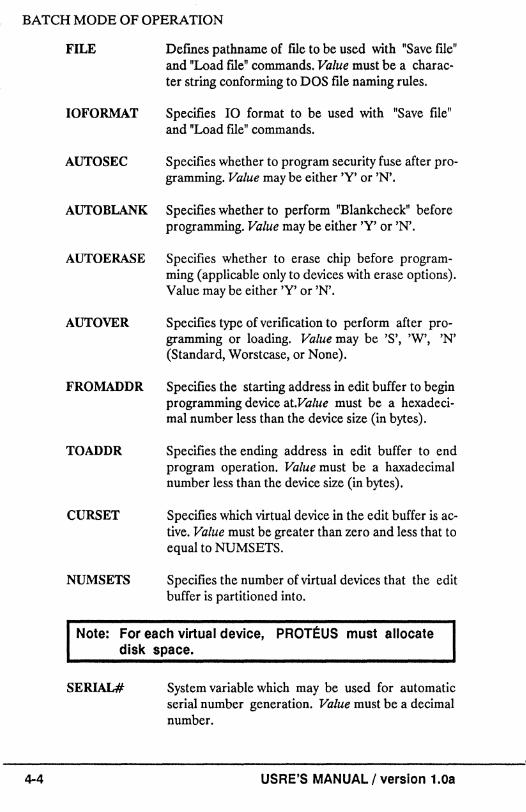
4.2.10. INIT variable value
Initializes one of the following "Options" or system variables.
AUTOINC Specifies whether to increment current set after programming. Value may be either 'Y' or 'N',
USRE'S MANUAL I version 1.0a 4-3
BATCH MODE OF OPERATION
4-4
FILE Dermes pathname of fUe to be used with "Save fUe" and "Load fUe" commands. Value must be a character string conforming to DOS fUe naming rules.
IOFORMAT Specifies 10 format to be used with "Save fUe" and "Load fUe" commands.
AUTOSEC Specifies whether to program security fuse after programming. Value may be either 'Y' or 'N'.
AUTO BLANK Specifies whether to perform "Blankcheck" before programming. Value may be either 'Y' or 'N'.
AUTOERASE Specifies whether to erase chip before programming (applicable only to devices with erase options). Value may be either 'Y' or 'N'.
AUTOVER Specifies type of verification to perform after programming or loading. Value may be'S', 'W', 'N' (Standard, Worstcase, or None).
FROMADDR Specifies the starting address in edit buffer to begin programming device at.Value must be a hexadecimal number less than the device size (in bytes).
TOAD DR Specifies the ending address in edit buffer to end program operation. Value must be a haxadecimal number less than the device size (in bytes).
CURSET Specifies which virtual device in the edit buffer is active. Value must be greater than zero and less that to equal to NUMSETS.
NUMSETS Specifies the number of virtual devices that the edit buffer is partitioned into.
Note: For each virtual device, PROTEUS must allocate disk space.
SERIAL# System variable which may be used for automatic serial number generation. Value must be a decimal number.
USRE'S MANUAL I version 1.0a
SERIAL#
REVISION#
BATCH MODE OF OPERATION
System variable which may be used for automatic serial number generation. Value must be a decimal number.
System variable which may be used for automatic revison number generation.
4.2.11. SETKEY key macro
Assigns macro to key. Therefore whenever user presses key, macro will be executed. Legals values for key are A Fl, A F2, ... A FlO.
Example:
SETKEY A Fl SELECT
4.2.12. MACRO name
Defines the start of a macro definition. Name can not be greater than 8 characters.
Note: Any batch commands may be used in macro definition.
4.2.13. ENDMAC
Defmes the end of a macro defmition.
4.2.14. RET
Returns control to PROTEUS system.
USRE'S MANUAL / version 1.0a 4-5

BATCH MODE OF OPERATION
This page left intentionally blank.
4-6 USRE'S MANUAL! version 1.0a
ALGORITHM DEVELOPMENT
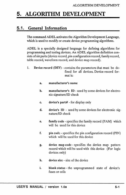
5. ALGORITHM DEVELOPMENT
5.1. General Information
The command ADEL activates the Algorithm Development Language, which is used to modify or create device programming algorithms.
ADEL is a specially designed language for defining algorithms for programming and testing devices. An ADEL algorithm defmition consists of six parts (device record, pin configuration record, family record, table record, waveform record, and device map record).
1. Device record (DEV) - contains the parameters that must be defined for all devices. Device record format is:
a. manufacturer's name
h. manufacturer's ID - used by some devices for electronic signaturellD check
c. device's part# - for display only
d. device's ID - used by some devices for electronic signaturellD check
e. family code - specifies the family record (FAM) which will be used for this device
f. pin code - specifies the pin configuration record (PIN) which will be used for this device
g. device map code - specifies the device map pattern record which will be used with this device (For logic devices only)
h. device size - size of the device
i. blank status - the unprogrammed state of device's fuses or cells
USER'S MANUAL / version 1.0a 5-1
ALGORITHM DEVELOPMENT
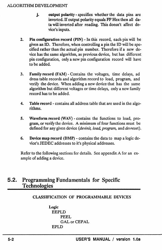
j. output polarity - specifies whether the data pins are inverted. If output polarity equals FF Hex then all data will inverted after reading. This doesn't affect device's inputs.
2. Pin configuration record (PIN) • In this record, each pin will be given an ID. Therefore, when controlling a pin the ID will be specified rather than the actual pin number. Therefore if a new device has the same algorithm, as previous device, but has different pin configuration, only a new pin configuration record will have to be added.
3. Family record (F AM) - Contains the voltages, time delays, ad dress table records and algorithm record to load, program, and verify the device. When adding a new device that has the same algorithm but different voltages or time delays, only a new family record has to be added.
4. Table record - contains all address table that are used in the algorithms.
S. Waveform record (W A V) • contains the functions to load, program, or verify the device. A minimum of four functions must be dermed for any given device (devini~ load, program, and devreset).
6. Device map record (DMP) - contains the data to map a logic device's JEDEC addresses to it's physical addresses.
Refer to the following sections for details. See appendix A for an example of adding a device.
5.2. Programming Fundamentals for Specific Technologies
5-2
CLASSIFICATION OF PROGRAMMABLE DEVICES
Logic EEPLD
PEEL GALorCEPAL
EPLD
USER'S MANUAL I version 1.0a
ALGORITHM DEVELOPMENT
PEEL
BipolarPLD Current source Voltage source
ECLPLD
Memory Single chip microcomputers with EPROM EPROM EEPROM Serial EEPROM High speed CMOS PROM Bipolar PROM
1. This is an electrically erasable logic device which is programmed and verified in parallel.
2. Rise times for high voltage pins must be slow. Use the slope command.
3. The parallel logic sequencer (2) must be selected.
4. Data will be programmed to and loaded from the device in parallel using put and get commands.
5. Addresses will be sent using the putentry command, possibly with an address lookup table.
6. The device erase function must be performed before programming, and must be included in the devinit() function for this device.
7. Program security fuse function, security() must be defined.
GAL or CEPAL
1 . This is an electrically erasable logic device which is programmed and verified in seria1. A row is addressed and shifted into the dedevices's serial shift register. Some GAL devices such as AMD's CEP ALs may program in serial, however, loaded in parallel.
USER'S MANUAL / version 1.0a 5-3
ALGORITHM DEVELOPMENT
2. Rise times for high voltage pins must be slow. Use the slope command.
3. Serial logic sequencer (3) must be selected.
4. Data will be programmed to, and loaded from the device in serial, using the sput, rsput, sget and rsget commands.
5. Addresses might be sent in parallel or in serial.
6. The device erase function must be performed before program ming and must be included in the devinit() function for this device.
7. Programsecurity() function must be defined.
EPLD
1. This is an ultra-violet, light erasable, logic device which is proprogrammed and verified in parallel. Use the put and get commands.
2. Rise times for high voltage pins are not critical.
3. Parallel logic sequencer (2) must be selected.
4. Device is programmed similar to a High Speed CMOS PROM, using INTELLIGENT or Super-Adaptive algorithms. For these these devices it is very critical that the algorithm is implemented correctly or some fuses may change state periodically after programming.
5. Program security() function must be defined.
Bipolar PLD (PAL)
1. This is a non-erasable logic device. It is addressed and loaded in parallel, however, only one fuse may be programmed at a time.
2. Parallel logic sequencer (2) must be selected.
5-4 USER'S MANUAL / version 1.0a
ALGORITHM DEVELOPMENT
3. Data will be programmed to and loaded from the device using the !orput statement and get command.
4. tDUTY must be defmed in the family record. This is the cooling time for the device after each high voltage pulse. If this value is too short, the device might not be able to program many fuses at one time.
5. These devices normally use high current. If the device cannot load or program, check the voltage drop at vee and high voltage pins. If the voltage is dropping, then raise it to compensate.
6. Program security() function must be defined.
Single Chip Microcomputer with EPROM
1. Is programmed like a normal EPROM except that a 4Mhz clock is required.
EPROM
1. This is an ultra-violet, light erasable memory device, which is programmed and loaded in parallel.
2. The memory sequencer (1) must be selected.
3. For many of these devices a programming algorithm (Le., Intelligent-I, Quick-pulse) must be defined.
4. It is important that the eE and OE pins are at their correct level. If the device cannot be read, this is normally the problem.
5. If a devices is read with a random checksum, then the device was not erased or programmed correctly or the vee voltage is not correct.
6. If a device cannot be programmed, then either the VPP voltage or the programming pulse width is incorrect.
USER'S MANUAL / version 1.0a 5-5
ALGORITHM DEVELOPMENT
EEPROM
1. This is an electrically erasable memory device which is programmed and loaded in parallel. It is normally loaded and programmed without high voltages.
2. The memory sequencer (1) must be selected.
3. It is important that the CE and OE pins are at their correct level. If the device cannot be read, this is normally the problem.
High Speed CMOS PROM
1. This is an ultra-violet, light erasable memory device, (pinout compatible with Bipolar PROMs) which is programmed and loaded in parallel.
2. The memory sequencer (1) must be selected.
3. A programming algorithm must be defined. This algorithm is critical and sometimes its parameters must be fme tuned for the device to program consistently. If random programming errors occur, it is normally a problem with the algorithm.
4. It is important that the CE and OE pins are at their correct level. If the device cannot be read, this is normally the problem.
Bipolar PROM
1. This is a non-erasable memory device. It is addressed and loaded in parallel, however only one fuse may be programmed at a time.
2. The memory sequencer (1) must be selected.
3. Data will be programmed to and loaded from the device using the !orput statement and get command.
4. tDU7Ymust be defmed in the family record. This is the cooling time for the device after each high voltage pulse. If this value is too short, the device might not be able to program many fuses at one time.
5-6 USER'S MANUAL / version 1.0a
ALGORITHM DEVELOPMENT
5. These devices normally use high current. If the device cannot load or program, check the voltage drop at vee and high voltage pins. If the voltage is dropping, raise it to compensate.
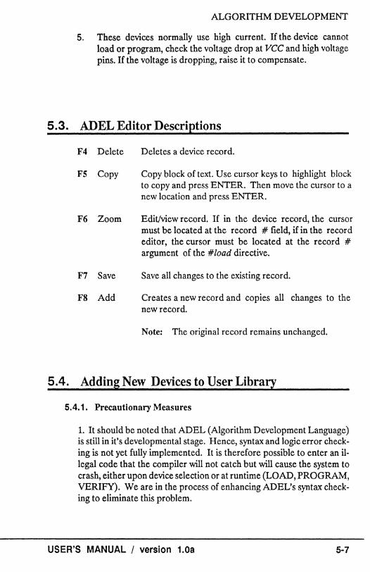
5.3. ADEL Editor Descriptions
F4 Delete
F5 Copy
F6 Zoom
F7 Save
F8 Add
Deletes a device record.
Copy block of text. Use cursor keys to highlight block to copy and press ENTER. Then move the cursor to a new location and press ENTER.
Edit/view record. If in the device record, the cursor must be located at the record # field, if in the record editor, the cursor must be located at the record # argument of the #load directive.
Save all changes to the existing record.
Creates a new record and copies all changes to the new record.
Note: The original record remains unchanged.
5.4. Adding New Devices to User Library
5.4.1. Precautionary Measures
1. It should be noted that ADEL (Algorithm Development Language) is still in it's developmental stage. Hence, syntax and logic error checking is not yet fully implemented. It is therefore possible to enter an illegal code that the compiler will not catch but will cause the system to crash, either upon device selection or at runtime (LOAD, PROGRAM, VERIFY). We are in the process of enhancing ADEL's syntax checking to eliminate this problem.
USER'S MANUAL / version 1.0a 5-7
ALGORITHM DEVELOPMENT
5-8
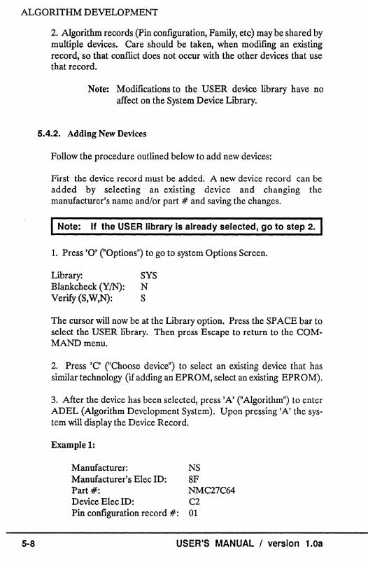
2. Algorithm records (Pin configuration, Family, etc) may be shared by multiple devices. Care should be taken, when modifing an existing record, so that conflict does not occur with the other devices that use that record.
Note: Modifications to the USER device library have no affect on the System Device Library.
5.4.2. Adding New Devices
Follow the procedure outlined below to add new devices:
First the device record must be added. A new device record can be added by selecting an existing device and changing the manufacturer's name and/or part # and saving the changes.
Note: If the USER library is already selected, go to step 2.
1. Press '0' ("Options") to go to system Options Screen.
Library: SYS Blankcheck (YIN): N Verify (S,W,N): S
The cursor will now be at the Library option. Press the SPACE bar to select the USER library. Then press Escape to return to the COMMANDmenu.
2. Press 'C' ("Choose device") to select an existing device that has similar technology (if adding an EPROM, select an existing EPROM).
3. After the device has been selected, press 'A' ("Algorithm") to enter ADEL (Algorithm Development System). Upon pressing 'A' the system will display the Device Record.
Example 1:
Manufacturer: Manufacturer's Elec ID: Part #: Device Elec ID:
NS SF NMC27C64 C2
Pin configuration record #: 01
USER'S MANUAL I version 1.0a
ALGORITHM DEVELOPMENT
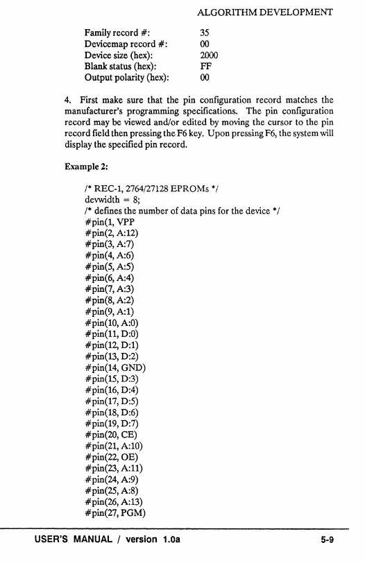
Family record #: 35 Devicemap record #: 00 Device size (hex): 2000 Blank status (hex): FF Output polarity (hex): 00
4. First make sure that the pin configuration record matches the manufacturer's programming specifications. The pin configuration record may be viewed and/or edited by moving the cursor to the pin record field then pressing the F6 key. Upon pressing F6, the system will display the specified pin record.
Example 2:
/* REC-l, 2764/27128 EPROMs */ devwidth = 8; !* defines the number of data pins for the device * / #pin(l, VPP #pin(2, A:12) #pin(3, A:7) #pin( 4, A:6) #pin(5, A:5) #pin(6, A:4) #pin(7, A:3) #pin(8, A:2) #pin(9, A:l) #pin(10, A:O) #pin(l1, D:O) #pin(12, D:l) #pin(13, D:2) #pin(14, GND) #pin(15, D:3) #pin(16, D:4) #pin(17, D:5) #pin(18, D:6) #pin(19, D:7) #pin(20, CE) #pin(21, A:I0) #pin(22, DE) #pin(23, A:ll) #pin(24, A:9) #pin(25, A:8) #pin(26, A:13) #pin(27, PGM)
USER'S MANUAL I version 1.08 5-9

ALGORITHM DEVELOPMENT
#pin(27, WE) #pin(28, VCC)
5-10
S. After modifying the record, press F8 if you want to save the changes as a new record, or F7 if you want to save changes to an existing record. If a new record is added, it's record # will be automatically assigned and the pin record # field of the Device record will be automatically updated.
6. Next, make sure that the family record matches specifications. The family record may be viewed and/or edited by moving the cursor to the family record field, then pressing the F6 key. Upon pressing F6, the system will display the specified family record.
Example 3:
1* REC-35, NS 27C64 EPROMs '" / VCCH = 6.00vcc; VPP = l3.00vppl; 1* See "Constants" - "Modifiers" '" / PW = Soous; RETRY = 20; OPW = 3; VCC = 5.00vcc; VPPL = 5.00vppl; tD = 10us; sequencer == 1; /'" selects memory device sequencer'" / #load(WA V, 1,2,3,4, 153) 1* loads waveforms'" /
7. Next, make sure that the waveform functions are according to specifications.
Note: A minimum of 4 functions must be defined: devinit, load, program, and devreset.
In Example 3, five functions are loaded: l-devinit, 3-load, 4-devreset and l53-program which calls 2-prog. To view and/or edit waveform records, move the cursor to the record # parameter of #load directive and press the F6 key. Upon pressing F6, the system will display the specified waveform record.
USER'S MANUAL / version 1.0a
ALGORITHM DEVELOPMENT
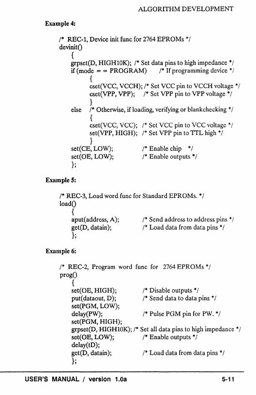
Example 4:
1* REC·l, Device init func for 2764 EPROMs "'/ devinitO
{ grpset(D, HIGHlOK); /'" Set data pins to high impedance'" / if (mode = = PROGRAM) 1* If programming device * /
{ cset(VCC, VCCH); 1* Set VCC pin to VeCH voltage */ cset(VPP, VPP); 1* Set VPP pin to VPP voltage */ }
else 1* Otherwise, if loading, verifying or blank checking '" / { cset(VCC, VCC); /* Set VCC pin to vce voltage * / set(VPP, HIGH); 1* Set VPP pin to TTL high "'/ }
set(CE, LOW); set(OE, LOW); };
Example 5:
1* Enable chip * / 1* Enable outputs * /
1* REC·3, Load word func for Standard EPROMs. * / 10adO
{ aput(address, A); get(D, datain); };
Example 6:
1* Send address to address pins * / /* Load data from data pins'" /
1* REC·2, Program word func for 2764 EPROMs * / progO
{ set(OE, HIGH); put(dataout, D); set(PGM, LOW); delay(PW); set(PGM, HIGH);
1* Disable outputs * / 1* Send data to data pins * /
/* Pulse PGM pin for PW. */
grpset(D, HIGH10K); 1* Set all data pins to high impedance * / set(OE, LOW); 1* Enable outputs "'/ delay(tD); get(D, datain); };
USER'S MANUAL / version 1.0a
/'" Load data from data pins'" /
5-11
ALGORITHM DEVELOPMENT
5-12
Example 7:
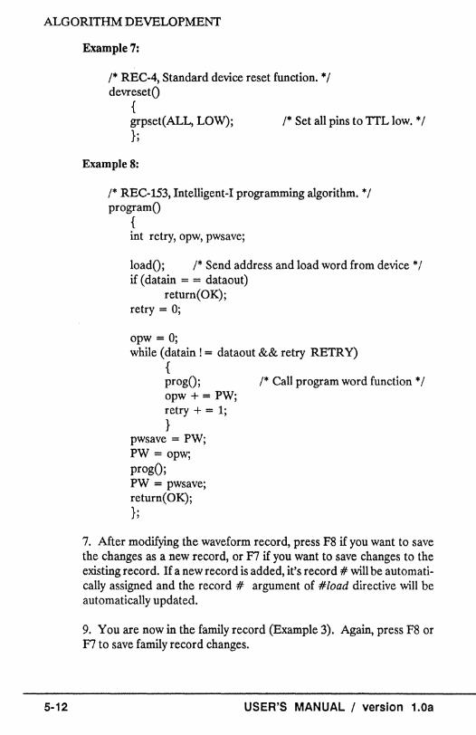
1* REC-4, Standard device reset function. >11/
devresetO { grpset(ALL, LOW); />11 Set all pins to TTL low. >11/
};
Example 8:
1* REC-153, Intelligent -I programming algorithm. >11/
programO { int retry, opw, pwsave;
loadO; 1* Send address and load word from device >11/
if (datain = = dataout) return(OK);
retry == 0;
opw = 0; while (datain! 0:: dataout && retry RETRY)
{ progO; 1* Call program word function >11/
opw + == PW; retry + == 1; }
pwsave == PW; PW = opw; progO; PW = pwsave; return(OK); };
7. After modifying the waveform record, press F8 if you want to save the changes as a new record, or F7 if you want to save changes to the existing record. If a new record is added, it's record # will be automatically assigned and the record # argument of #load directive will be automatically updated.
9. You are now in the family record (Example 3). Again, press F8 or F7 to save family record changes.
USER'S MANUAL I version 1.0a
ALGORITHM DEVELOPMENT
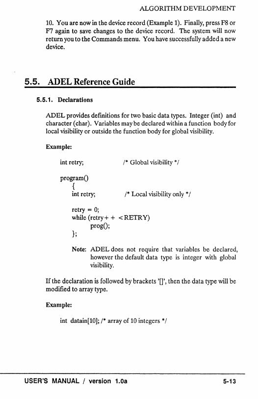
10. You are now in the device record (Example 1). Finally, press F8 or F7 again to save changes to the device record. The system will now return you to the Commands menu. You have successfully added a new device.
5.5. ADEL Reference Guide
5.5.1. Declarations
ADEL provides definitions for two basic data types. Integer (int) and character ( char). Variables may be declared within a function body for local visibility or outside the function body for global visibility.
Example:
int retry; 1* Global visibility" /
programO { int retry; 1* Local visibility only * /
retry = 0; while (retry + + < RETRY)
progO; };
Note: ADEL does not require that variables be declared, however the default data type is integer with global visibility.
If the declaration is followed by brackets '[]" then the data type will be modified to array type.
Example:
int datain[10]; 1* array of 10 integers" /
USER'S MANUAL / version 1.0a 5-13
ALGORITHM DEVELOPMENT
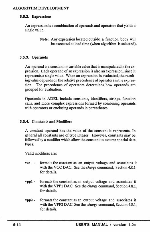
5.5.2. Expressions
An expression is a combination of operands and operators that yields a single value.
Note: Any expression located outside a function body will be executed at load time (when algorithm is selected).
5.5.3. Operands
An operand is a constant or variable value that is manipulated in the expression. Each operand of an expression is also an expression, since it represents a single value. When an expression is evaluated, the resulting value depends on the relative precedence of operators in the expression. The precedence of operators determines how operands are grouped for evaluation.
Operands in ADEL include constants, identifiers, strings, function calls, and more complex expressions formed by combining operands with operators or enclosing operands in parentheses.
5.5.4. Constants and Modifiers
A constant operand has the value of the constant it represents. In general all constants are of type integer. However, constants may be followed by a modifier which allow the constant to assume special data types.
Valid modifiers are:
vee - formats the constant as an output voltage and associates it with the VCC DAC. See the charge command, Section 4.8.1, for details.
vpp1 - formats the constant as an output voltage and associates it with the VPP1 DAC. See the charge command, Section 4.8.1, for details.
vpp2 - formats the constant as an output voltage and associates it with the VPP2 DAC. See the charge command, Section 4.8.1, for details.
5-14 USER'S MANUAL I version 1.0a
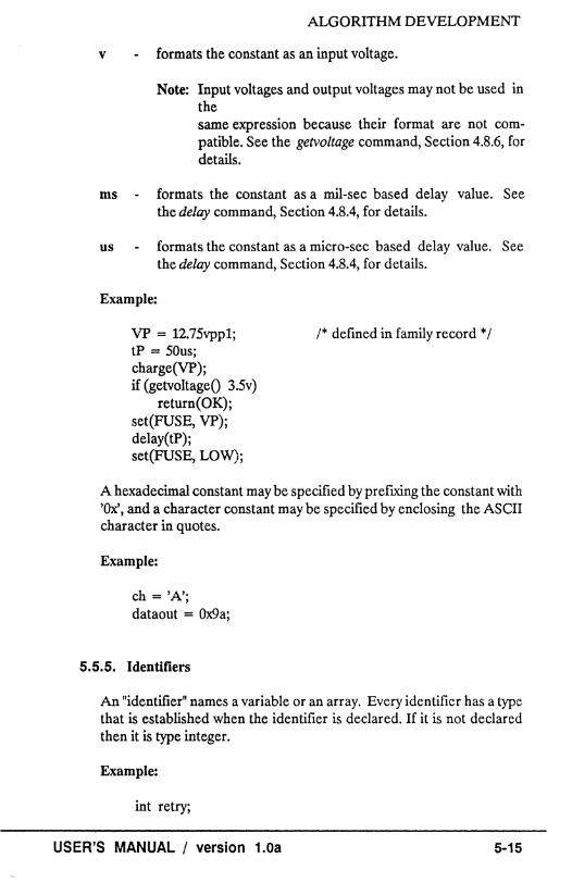
ALGORITHM DEVELOPMENT
v formats the constant as an input voltage.
Note: Input voltages and output voltages may not be used in the same expression because their format are not compatible. See the getvoltage command, Section 4.8.6, for details.
ms formats the constant as a mil-sec based delay value. See the delay command, Section 4.8.4, for details.
us formats the constant as a micro-sec based delay value. See the delay command, Section 4.8.4, for details.
Example:
VP = 12.7Svppl; tP = 50us; charge(VP); if (getvoltageO 3.5v)
return(OK); set(FUSE, VP); delay(tP); set (FUSE, LOW);
/* defined in family record * /
A hexadecimal constant may be specified by prefixing the constant with 'Ox', and a character constant may be specified by enclosing the ASCII character in quotes.
Example:
ch = 'A'; dataout = Ox9a;
5.5.5. Identifiers
An "identifier" names a variable or an array. Every identifier has a type that is established when the identifier is declared. If it is not declared then it is type integer.
Example:
int retry;
USER'S MANUAL / version 1.0a 5-15

ALGORITHM DEVELOPMENT
5.5.6. Strings
A "string literal" is a character or sequence of adjacent characters enclosed in double quotation marks.
Example:
error("Device 1D mismatch.");
5.5.7. Function Calls
Function Calls are specified as follows: a function name followed by function arguments, separated by commas, and enclosed in parentheses.
Example:
say(10, 20, "calling devchk function"); devchk(l);
5.5.S. Operators
5-16
Operators specify how the operand(s) of the expression are manipulated.
ADEL operators take one (unary) or two (binary) operands. Assignment operators include both unary or binary operators.
Assignment Operators
The assignment operators in ADEL can both transform and assign values in a single operation. Using a compound assignment operator to replace two separate operation can make your algorithms smaller and more efficient. ADEL provides the following assignment operators:
++
*=
1* %=
unary increment unary decrement simple assignment multiplication assignment division assignment remainder assignment
USER'S MANUAL / version 1.0a
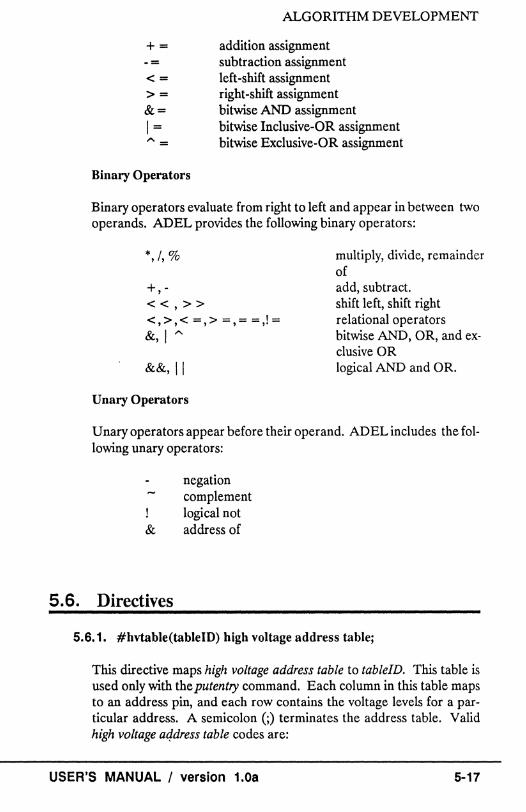
ALGORITHM DEVELOPMENT
+ = addition assignment -= subtraction assignment < = left-shift assignment > = right-shift assignment & = bitwise AND assignment 1 = bitwise Inclusive-OR assignment '" = bitwise Exclusive-OR assignment
Binary Operators
Binary operators evaluate from right to left and appear in between two operands. ADEL provides the following binary operators:
*,/, %
+, -< <,» <,>,< =,> =,= =,!= &,1 A
&&,11
Unary Operators
multiply, divide, remainder of add, subtract. shift left, shift right relational operators bitwise AND, OR, and exclusive OR logical AND and OR.
Unary operators appear before their operand. ADEL includes the following unary operators:
negation complement logical not
& address of
5.6. Directives
5.6.1. #hvtable(tableID) high voltage address table;
This directive maps high voltage address table to tableID. This table is used only with the putentry command. Each column in this table maps to an address pin, and each row contains the voltage levels for a particular address. A semicolon (j) terminates the address table. Valid high voltage aqdress table codes are:
USER'S MANUAL I version 1.0a 5-17
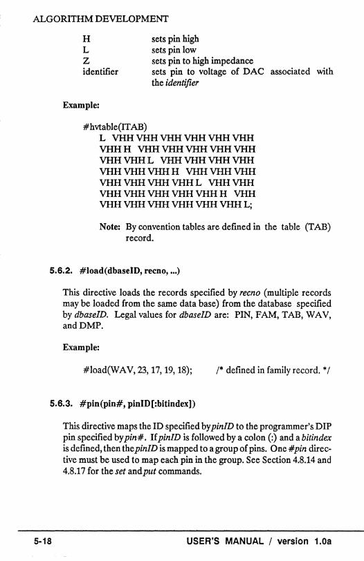
ALGORITHM DEVELOPMENT
H L
sets pin high sets pin low
Z identifier
sets pin to high impedance sets pin to voltage of DAC associated with the identifier
Example:
#hvtable(ITAB) L VHH VHH VHH VHH VHH VHH VHH H VHH VHH VHH VHH VHH VHH VHH L VHH VHH VHH VHH VHH VHH VHH H VHH VHH VHH VHH VHH VHH VHH L VHH VHH VHH VHH VHH VHH VHH H VHH VHH VHH VHH VHH VHH VHH L;
Note: By convention tables are defined in the table (TAB) record.
5.6.2. #load(dbaselD, recno, ... )
This directive loads the records specified by recno (multiple records may be loaded from the same data base) from the database specified by dbaselD. Legal values for dbaselD are: PIN, PAM, TAB, WAV, andDMP.
Example:
#load(WAV, 23,17,19,18); 1* defined in family record. '" /
5.6.3. #pin(pin#, pinlD[:bitindex])
This directive maps the ID specified by pinlD to the programmer's DIP pin specified bypin#. IfpinlD is followed by a colon (:) and a bitindex is defined, then the pinlD is mapped to a group of pins. One #pin directive must be used to map each pin in the group. See Section 4.8.14 and 4.8.17 for the set and put commands.
USER'S MANUAL / version 1.0a
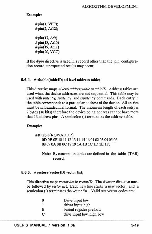
ALGORITHM DEVELOPMENT
Example:
#pin(1, VPP); #pin(2, A:12);
#pin(17, A:9) #pin(18, A:10) #pin(19, A:ll) #pin(20, VCC)
If the #pin directive is used in a record other than the pin configuration record, unexpected results may occur.
5.6.4. #ttltable(tableID) ttl level address table;
This directive maps ttl level address table to tableID. Address tables are used when the device addresses are not sequential. This table may be used withputent1)', sputent1)', and rsputent1)' commands. Each entry in the table corresponds to a particular address of the device. All entries must be in hexadecimal format. The maximum length of each entry is 2 bytes (16 bits) therefore the device being address cannot have more that 16 address pins. A semicolon (;) terminates the address table.
Example:
#ttltable(ROW ADDR) ®~~WllUDw~MMmroM~~ 0809 OA OB OC 18 19 1A 1B 1C ID 1E 1F;
Note: By convention tables are defined in the table (TAB) record.
5.6.5. #Vectors(vectorID) vector list;
This directive maps vector list to vectorID. The #vector directive must be followed by vector list. Each new line starts a new vector, and a semicolon (;) terminates the vector list. Valid test vector codes are:
o Drive input low 1 driver input high B buried register preload C drive input low, high, low
USER'S MANUAL I version 1.0a 5-19
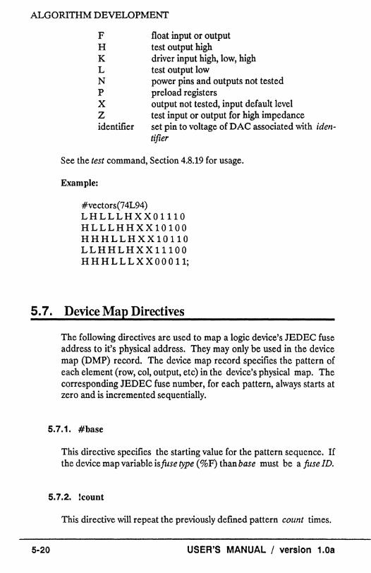
ALGORITHM DEVELOPMENT
F float input or output H test output high K driver input high, low, high L test output low N power pins and outputs not tested P preload registers X output not tested, input default level Z test input or output for high impedance identifier set pin to voltage ofDAC associated with iden
tifier
See the test command, Section 4.8.19 for usage.
Example:
#vectors(74L94) LHLLLHXXO 1110 HLLLHHXX 10100 HHHLLHXX 10 110 LLHHLHXX11100 HHHLLLXXOOO 11;
5.7. Device Map Directives
The following directives are used to map a logic device's JEDEC fuse address to it's physical address. They may only be used in the device map (DMP) record. The device map record specifies the pattern of each element (row, col, output, etc) in the device's physical map. The corresponding JEDEC fuse number, for each pattern, always starts at zero and is incremented sequentially.
5.7.1. #base
This directive specifies the starting value for the pattern sequence. If the device map variable isjUse type (%F) than base must be a jUse/D.
5.7.2. !count
This directive will repeat the previously defined pattern count times.
5-20 USER'S MANUAL / version 1.0a

ALGORITHM DEVELOPMENT
Example PAL 16L8 device map record:
%T #AND2048 %R #0 + 32 "256 2048 %C #0 + 1 "'322048 %0 #0 + 256 2048 %R #3264
5.7.3. Device Record Format
%F #base > range ..... %C # base [ + incafter] ['" resetafter] > range .... . %R # base [ + incafter] ['" reset after ] > range .... . %0 #base [ + incafter] ['" reset after] > range .... . %E #base range .....
5.7.4. %elementlD
T fuse types R row addresses C col addresses o outputs E edit buffer row lengths
5.7.5. + incafter
This directive increments the pattern after incafter number of fuses have been sequenced.
5.7.6. > resetafter
This directive sequences the pattern specified by preceding directives (%, #, +, A) for range number offuses.
5.7.7. '" restafter
This directive resets the pattern after resetafter number of fuses have been sequenced. The pattern is always reset to base.
USER'S MANUAL / version 1.0a 5-21
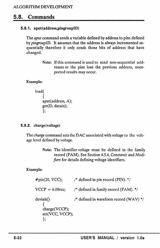
5.8. Commands
5.S.1. aput(address,pingroupJD)
The aput command sends a variable defmed by address to pins defmed by pingroupID. It assumes that the address is always incremented sequentially therefore it only sends those bits of address that have changed.
Example:
Note: If this command is used to send non-sequential addresses or the pins lose the previous address, unexpected results may occur.
load( { aput(address, A); get(D, datain); };
5.8.2. charge (voltage)
The charge command sets the DAC associated with voltage to the voltage level defined by voltage.
Example:
Note: The identifier voltage must be defmed in the family record (FAM). See Section 4.5.4, Constants and Modifiers for details defining voltage identifiers.
#pin(20, VCC); /* defined in pin record (PIN). */
VCCP = 6.00vcc; /* defined in family record (F AM). * /
devinitO /* defined in waveform record (W A V) * / { charge(VCCP); set(VCC, VCCP); };
5-22 USER'S MANUAL / version 1.0a
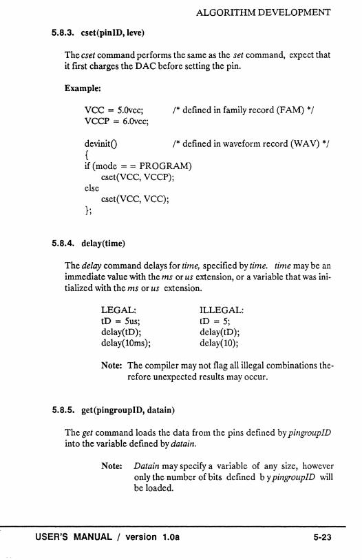
ALGORITHM DEVELOPMENT
5.8.3. cset(pinID,leve)
The eset command performs the same as the set command, expect that it ftrst charges the DAC before setting the pin.
Example:
VCC = S.Ovcc; VCCP = 6.Ovcc;
/* defined in family record (F AM) * /
devinitO /* defined in waveform record (W A V) * / { if (mode = = PROGRAM)
cset(VCC, VCCP); else
cset(VCC, VCC); };
5.8.4. delay(time)
The delay command delays for time, specified by time. time may be an immediate value with the ms or us extension, or a variable that was initialized with the ms or us extension.
LEGAL: tD = Sus; delay(tD); delay(lOms);
ILLEGAL: tD = S; delay(tD); delay(lO);
Note: The compiler may not flag all illegal combinations therefore unexpected results may occur.
5.8.5. get(pingroupID, datain)
The get command loads the data from the pins defined by pingroupID into the variable defined by datain.
Note: Datain may specify a variable of any size, however only the number of bits defined by pingroupID will be loaded.
USER'S MANUAL / version 1.0a 5-23
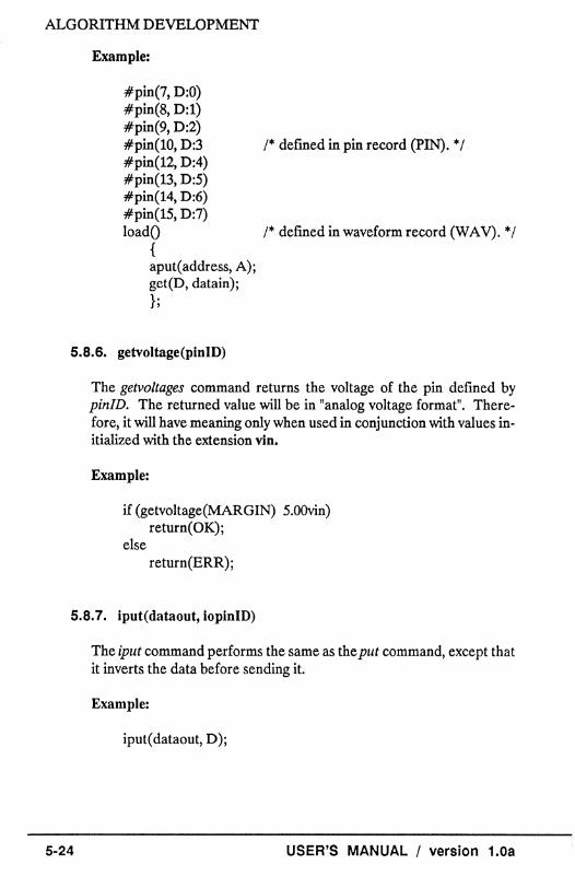
ALGORITHM DEVELOPMENT
Example:
#pin(7, D:O) #pin(8, D:l) #pin(9, D:2) #pin(10, D:3 /* defined in pin record (PIN). */ #pin(12, D:4) #pin(13, D:5) #pin(14, D:6) #pin(lS, D:7) loadO 1* defined in waveform record (W A V). * /
{ aput(address, A)j get(D, datain)j }j
5.S.6. getvoltage(pinlD)
The getvoltages command returns the voltage of the pin defined by pin/D. The returned value will be in "analog voltage format". Therefore, it will have meaning only when used in conjunction with values initialized with the extension vin.
Example:
if (getvoltage(MARGIN) 5.00vin) return(OK)j
else return(ERR);
5.S.7. iput(dataont,lopinlD)
5-24
The iput command performs the same as the put command, except that it inverts the data before sending it.
Example:
iput(dataout, D)j
USER'S MANUAL I version 1.0a
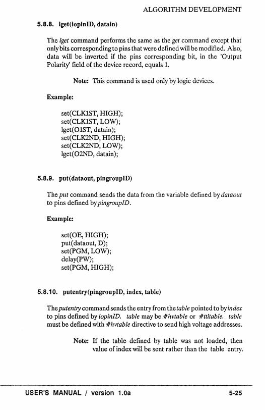
ALGORITHM DEVELOPMENT
5.S.S. Iget(iopinID, datain)
The 1get command performs the same as the get command except that only bits corresponding to pins that were defined will be modified. Also, data will be inverted if the pins corresponding bit, in the 'Output Polarity' field of the device record, equals 1.
Note: This command is used only by logic devices.
Example:
set(CLKlST, HIGH); set(CLKlST, LOW); Iget(OlST, datain); set(CLK2ND, HIGH); set(CLK2ND, LOW); Iget(02ND, datain);
5.S.9. put(dataout, pingroupID)
The put command sends the data from the variable defined by dataout to pins defmed by pingroupID.
Example:
set(OE, HIGH); put(dataout, D); set(PGM, LOW); delay(PW); set(PGM, HIGH);
5.8.10. putentry(pingroupID, index, table)
Theputentry command sends the entry from thetable pointed to by index to pins defmed by iopinID. table may be #hvtable or #ttltable. table must be defmed with #hvtable directive to send high voltage addresses.
Note: If the table defined by table was not loaded, then value of index will be sent rather than the table entry.
USER'S MANUAL / version 1.0a
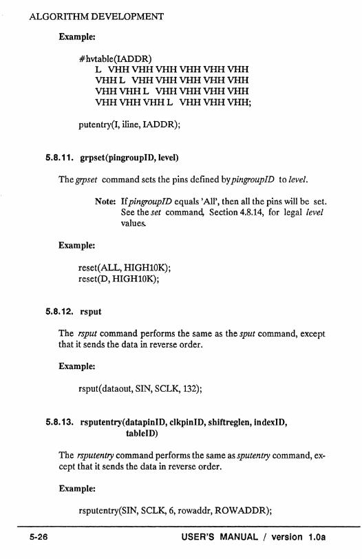
ALGORITHM DEVELOPMENT
Example:
#hvtable(IADDR) L VHH VHH VHH VHH VHH VHH VHH L VHH VHH VHH VHH VHH VHH VHH L VHH VHH VHH VHH VHH VHH VHH L VHH VHH VHH;
putentry(I, iline, IADDR);
5.8.11. grpset(pingroupID, level)
The grpset command sets the pins defined by pingroupID to level.
Example:
Note: JfpingroupID equals 'All', then all the pins will be set. See the set command, Section 4.8.14, for legal level values.
reset(ALL, HIGH10K); reset(D, HIGHI0K);
5.8.12. rsput
The rsput command performs the same as the sput command, except that it sends the data in reverse order.
Example:
rsput( data out, SIN, SeLK, 132);
5.8.13. rsputentry(datapinID, cIkpinID, shiftreglen, indexID, tableID)
5-26
The rsputentry command performs the same as sputentry command, except that it sends the data in reverse order.
Example:
rsputentry(SIN, SeLK, 6, rowaddr, ROWADDR);
USER'S MANUAL / version 1.0a
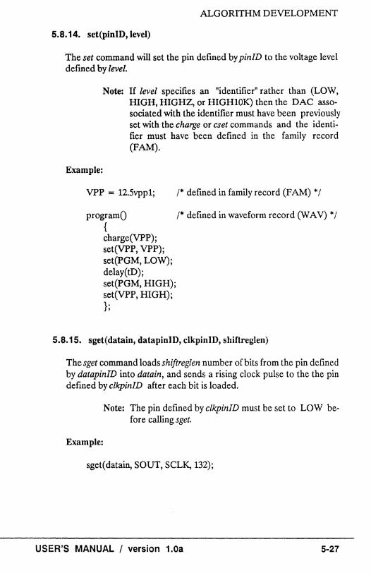
ALGORITHM DEVELOPMENT
5.8.14. set(pinlD, level)
The set command will set the pin defIned by pinID to the voltage level defIned by level.
Example:
Note: If level specifies an "identifier" rather than (LOW, HIGH, HIGHZ, or HIGH 10K) then the DAC assosociated with the identifier must have been previously set with the charge or cset commands and the identifIer must have been defIned in the family record (FAM).
VPP = 12.5vppl; /* defined in family record (FAM) */
programO 1* defIned in waveform record (W A V) * / { charge(VPP); set(VPP, VPP); set(PGM, LOW); delay(tD); set(PGM, HIGH); set(VPP, HIGH); };
5.8.15. sget(datain, datapinlD, clkpinlD, shiftreglen)
The sget command loads shiftreglen number of bits from the pin defIned by datapinID into datain, and sends a rising clock pulse to the the pin defined by clkpinID after each bit is loaded.
Example:
Note: The pin defined by clkpinID must be set to LOW before calling sget.
sget( datain, SOUT, SCLK, 132);
USER'S MANUAL / version 1.0a 5-27
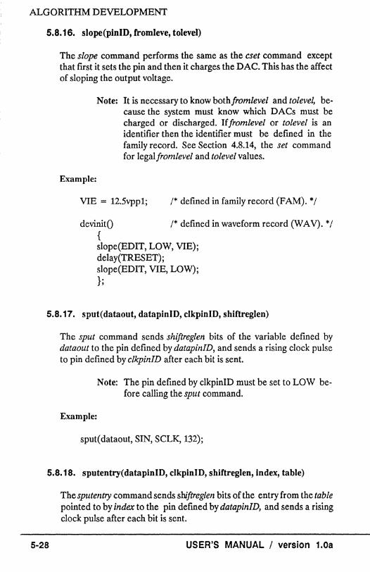
ALGORITHM DEVELOPMENT
5.8.16. slope(pinID, Cromleve, tolevel)
The slope command performs the same as the cset command except that ftrst it sets the pin and then it charges the DAC. This has the affect of sloping the output voltage.
Example:
Note: It is necessary to know bothjrom/eve/ and to/eve/, because the system must know which DACs must be charged or discharged. If/rom/eve/ or to/evel is an identifter then the identifier must be deftned in the family record. See Section 4.8.14, the set command for legal/romleve! and tolevel values.
VIE = 12.5vpp1; 1* defined in family record (FAM). */
devinitO 1* defined in waveform record (W A V). * / { slope(EDIT, LOW, VIE); delay(TRESET); slope(EDIT, VIE, LOW); };
5.8.17. sput(dataout, datapinID, clkpinID, shiftregJen)
The sput command sends shiftreg/en bits of the variable deftned by dataout to the pin defined by datapinID, and sends a rising clock pulse to pin deftned by C/kpinID after each bit is sent.
Example:
Note: The pin defined by clkpinID must be set to LOW before calling the sput command.
sput(dataout, SIN, SCLK, 132);
5.8.18. sputentry(datapinID, clkpinID, shiftreglen, index, table)
5-28
The sputentry command sends shi/treglen bits of the entry from the table pointed to by index to the pin defined by datapinID, and sends a rising clock pulse after each bit is sent.
USER'S MANUAL I version 1.0a
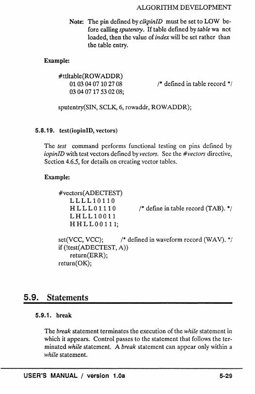
ALGORITHM DEVELOPMENT
Note: The pin defmed by c/kpinID must be set to LOW before calling sputentry. If table defmed by table wa not loaded, then the value of index will be set rather than the table entry.
Example:
#ttltable(ROW ADDR) 01 03 04 07 10 27 08 03040717530208;
1* defined in table record * /
sputentry(SIN, SCLK, 6, rowaddr, ROWADDR);
5.8.19. test(iopinID, vectors)
The test command performs functional testing on pins defined by iopinID with test vectors defined by vectors. See the #vectors directive, Section 4.6.5, for details on creating vector tables.
Example:
#vectors(ADECTEST) LLLLI0II0 HLLLOl110 LHLLI0011 HHLLOO 111;
/* define in table record (TAB). */
set(VCC, VCe); 1* defined in waveform record (WAV). */ if (!test(ADECTEST, A))
return(ERR) ; return(OK);
5.9. Statements
5.9.1. break
The break statement terminates the execution of the while statement in which it appears. Control passes to the statement that follows the terminated while statement. A break statement can appear only within a while statement.
USER'S MANUAL / version 1.0a 5-29
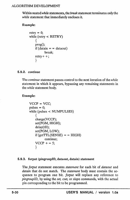
ALGORITHM DEVELOPMENT
Within nested while statements, the break statement terminates only the while statement that immediately encloses it.
Example:
retry = 0; while (retry < RETRY)
{ progO; if (datain = = dataout)
break; retry+ +; }
5.9.2. continue
The continue statement passes control to the next iteration of the while statement in which it appears, bypassing any remaining statements in the while statement body.
Example:
VCCP = VCC; pulses = 0; while (pulses < NUMPULSES)
{ charge(VCCP); set(PGM, HIGH); delay(tD); set(PGM, LOW); if (getTTL(SENSE) = = HIGH)
continue; VCCP + = 5; }
5.9.3. Corput (pingrouplD, dataout, datain) statement
5-30
The forput statement executes statement for each bit of dataout and datain that do not match. The statement body must contain the sequence to program one bit. forput will replace any reference to pingroupID, by using the set, cset, or slope commands, with the actual pin corresponding to the bit to be programmed.
USER'S MANUAL I version 1.0a

Example:
ALGORITHM DEVELOPMENT
Note: Before calling the !orput statement, data in must be loaded with the contents of the pins defined by pingroupID.
Iget(OlST, datain); forput(OlST, datain, dataout)
{ set (Vee, VHH); delay(tD); set(OlST, VHH); delay(tP); set(OlST, HIGHIOK); delay(tD); set (Vee, Vee); delay( tDUTY); }
5.9.4. if (expression) statementl [else statement2]
The body of an if statement is executed selectively, depending on the value of expression, as described below: Execution proceeds as follows:
a. If expression is true (non-zero), statementl is executed.
b. If expression is false, statement2 is executed.
c. If expression is false and the else clause is omitted, statementl is ignored.
5.9.5. return [expression]
The return statement terminates the execution of the function in which it appears and returns control to the calling function. Execution resumes in the calling function at the point immediately following the call. If expression is omitted, the return value of the function is undefmed.
USER'S MANUAL I version 1.0a 5-31
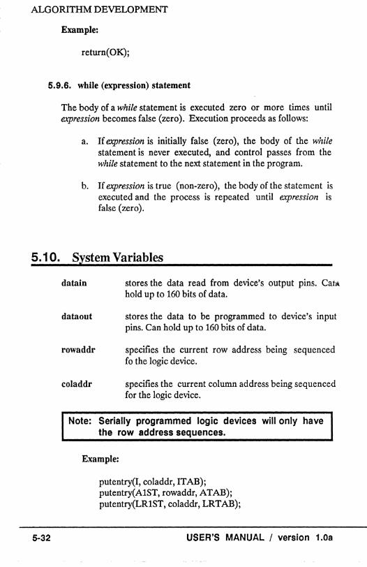
ALGORITHM DEVELOPMENT
Example:
return(OK);
5.9.6. while (expression) statement
The body of a while statement is executed zero or more times until expression becomes false (zero). Execution proceeds as follows:
a. If expression is initially false (zero), the body of the while statement is never executed, and control passes from the while statement to the next statement in the program.
b. If expression is true (non-zero), the body of the statement is executed and the process is repeated until expression is false (zero).
5.10. System Variables
5-32
datain
dataout
rowaddr
coladdr
stores the data read from device's output pins. Call1i: hold up to 160 bits of data.
stores the data to be programmed to device's input pins. Can hold up to 160 bits of data.
specifies the current row address being sequenced fo the logic device.
specifies the current column address being sequenced for the logic device.
Note: Serially programmed logic devices will only have the row address sequences.
Example:
putentry(I, coladdr, ITAB); putentry(A1ST, rowaddr, ATAB); putentry(LR1ST, coladdr, LRTAB);
USER'S MANUAL / version 1.0a
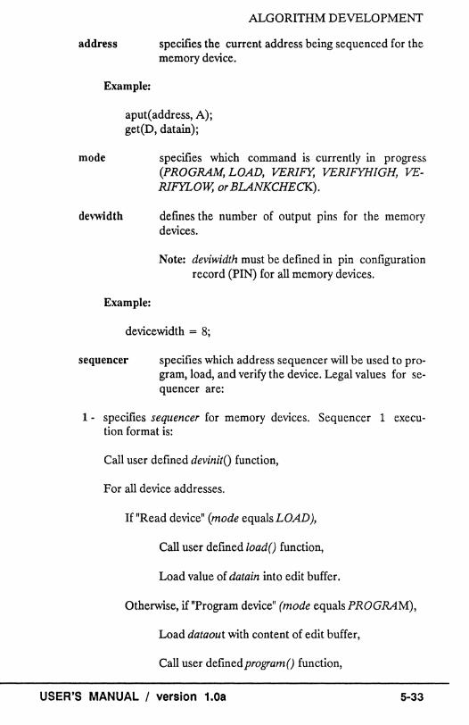
address
ALGORITHM DEVELOPMENT
specifies the current address being sequenced for the memory device.
Example:
mode
devwidth
aput(address, A); get(D, datain);
specifies which command is currently in progress (PROGRAM, LOAD, VERIFY, VERIFYHIGH, VERIFYLOw, or BLANKCHECK).
defmes the number of output pins for the memory devices.
Note: deviwidth must be defined in pin configuration record (PIN) for all memory devices.
Example:
devicewidth = 8;
sequencer specifies which address sequencer will be used to program, load, and verify the device. Legal values for sequencer are:
1 - specifies sequencer for memory devices. Sequencer 1 execution format is:
Call user defined devinitO function,
For all device addresses.
If "Read device" (mode equals LOAD),
Call user defined load() function,
Load value of datain into edit buffer.
Otherwise, if "Program device" (mode equals PROGRAM),
Load dataout with content of edit buffer,
Call user defined program () function,
USER'S MANUAL / version 1.0a 5-33
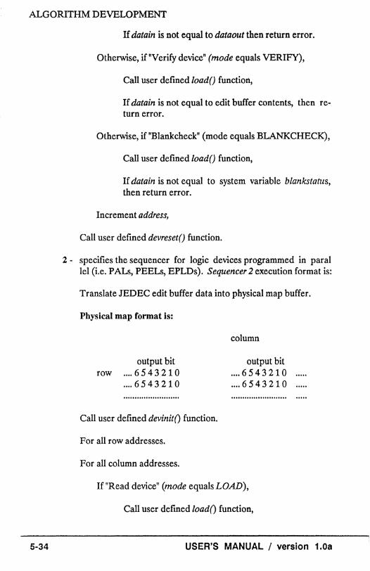
ALGORITHM DEVELOPMENT
5-34
If datain is not equal to dataout then return error.
Otherwise, if "Verify device" (mode equals VERIFY),
Call user defined loadO function,
If datain is not equal to edit buffer contents, then return error.
Otherwise, if "Blankcheck" (mode equals BLANKCHECK),
Call user defined loadO function,
If datain is not equal to system variable blankstatus, then return error.
Increment address,
Call user defined devresetO function.
2· specifies the sequencer for logic devices programmed in paral lel (i.e. PALs, PEELs, EPLDs). Sequencer 2 execution format is:
Translate JEDEC edit buffer data into physical map buffer.
Physical map format is:
output bit row .... 6 5 4 3 2 1 0
.... 6543210
column
output bit .... 6543210 .... 6543210
Call user defined devinit() function.
For all row addresses.
For all column addresses.
If "Read device" (mode equals LOAD),
Call user defined load() function,
USER'S MANUAL I version 1.08
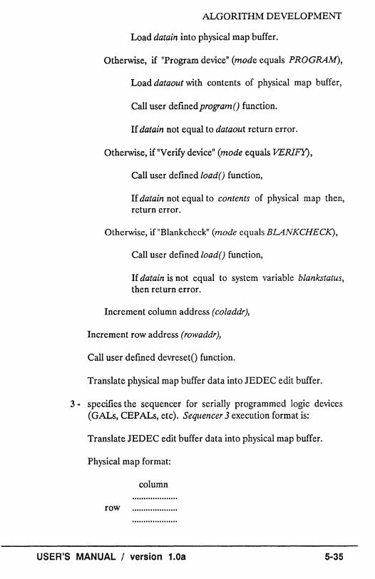
ALGORITHM DEVELOPMENT
Load datain into physical map buffer.
Otherwise, if "Program device" (mode equals PROGRAM),
Load dataout with contents of physical map buffer,
Call user defmed program () function.
If datain not equal to dataout return error.
Otherwise, if "Verify device" (mode equals VERIFY),
Call user defined load() function,
If datain not equal to contents of physical map then, return error.
Otherwise, if "Blankcheck" (mode equals BLANKCHECK),
Call user defined load() function,
If datain is not equal to system variable blankstatus, then return error.
Increment column address (co/addr),
Increment row address (rowaddr),
Call user defined devresetO function.
Translate physical map buffer data into JEDEC edit buffer.
3· specifies the sequencer for serially programmed logic devices (GALs, CEPALs, etc). Sequencer 3 execution format is:
Translate JEDEC edit buffer data into physical map buffer.
Physical map format:
column
row
USER'S MANUAL / version 1.0a 5-35

ALGORITHM DEVELOPMENT
5-36
Call user defined devinitO function,
For all row addresses.
If "Read device" (mode equal LOAD),
Call user defined loadO function,
Load datain into physical map buffer.
Otherwise, if "Program device" (mode equals PROGRAM),
Load dataout with contents of physical map buffer.
Call user defined program 0 function,
If datain is not equal to dataout return error.
Otherwise, if "Verify device" (mode equals VERIFY),
Call user defined /oadO function,
If datain is not equal to contents of physical map, then return error.
Otherwise, if "Blank check" (mode equals BLANKCHECK) ,
Call user defined /oadO function,
If datain not equal to system variable blankstatus then return error.
Increment row address (rowaddr),
Call user defined devresetO function,
Translate physical map buffer data into JEDEC edit buffer.
4 - specifies the sequencer for directly programmed logic devices (PLUSes, PLSes, etc). Sequencer 4 execution format is:
Call user defined devinitO function,
For all JEDEC addresses.
USER'S MANUAL I version 1.08

ALGORITHM DEVELOPMENT
Row address (rowaddr) equals row address corresponding to current JEDEC fuse address (as defined in device map),
Column address (coladdr) equals column address corresponding to current JEDEC fuse address (as defined in device map),
If "Read device" (mode equals LOAD),
Call user defined loadO function.
Load datain into JEDEC edit buffer.
Otherwise, if "Program device" (mode equals PROGRAM),
Load dataout with contents of JEDEC edit buffer,
Call user defmedprogramO function.
If datain is not equal to dataout, return error.
Otherwise, if "Verify device" (mode equals VERIFY),
Call user defined 10adO function
If datain not equal to contents of JEDEC edit buffer then return error.
Otherwise, if "Blankcheck" (mode equals BLANKCHECK),
Call user defined loadO function,
If datain not equal to system variable blankstatus, then return error,
Increment JEDEC address.
Call user defined devreset() function.
USER'S MANUAL I version 1.0a 5-37
ALGORITHM DEVELOPMENT
5.11. System Constants
5-38
LOAD system variable mode will equal LOAD when "Read device" in progress.
PROGRAM system variable mode will equal PROGRAM when "Program device" is in progress.
VERIFY system variable mode will equal VERIFY when "Verify device" (during standard verify pass).
VERIFYHIGH system variable mode will equal VERIFYHIGH when I1Verify device" is in progress (during high VCC verify pass).
VEFIFYLOW system variable mode will equal VERIFYLOW when "Verify device l1 is in progress (during low VCC verify pass).
BLANKCHECK system variable mode will equal BLANKCHECK when "Blankcheck" is in progress.
Example:
if (mode = = PROGRAM) cset(VCe, Vcep);
USER'S MANUAL / version 1.0a

IF YOU HA VB DIFFICULTIES
6. If You Have Difficulties
6.1 . What To Do:
Before calling B&C Microsystems make sure you have faxed or mailed a copy of the filled-out Registration Card enclosed in this manual. When calling for Customer Support, have the ruled out Registration Card in front of you for referencing information.
We advise you to read the following section, "MOST COMMON QUESTIONS", before calling. There is a good chance that you will fmd the answer to your question in this section.
The following is a list of symptoms and associated instructions that you should follow before calling for Customer Support:
The PROTEUS Software doesn't install successfully: • Check if you have enough space on your hard disk or floppy disk drive. You need at least 700KB of space in order to install the software.
The program comes up in DEMO mode: • This signifies that the hardware is not responding. • Verify that the PROTEUS is powered-up. The Power LED on the Adapter Module should be ON. • Check if your printer port is functioning correctly by connecting a printer to your parallel printer port and doing a test printout. Do this with the cable received with PROTEUS in order to check both, your printer port and the cable.
The programmer does not pass selfdiagnostics and autocalibration: • Make sure you do not have a device inserted in the ZIF socket.
You cannot read or program a device successfully: • Check if the part is damaged.
USER'S MANUAL / version 1.0a 6-1
IF YOU HAVE DIFFICULTIES
6.2. Most Common Questions:
(This Section will be expanded in the next manual release.)
6-2 USER'S MANUAL I version 1.0a
APPENDIX A
APPENDIX A PROTEUS PROGRAMMER SPECIFICATIONS
USER'S MANUAL I version 1.0a A·1
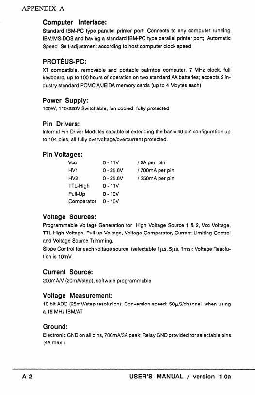
APPENDIX A
A·2
Computer Interface: Standard IBM·PC type parallel printer port; Connects to any computer running
IBM/MS·DOS and having a standard IBM·PC type parallel printer port; Automatic
Speed Self·adjustment according to host computer clock speed
PROTEUS·PC: XT compatible, removable and portable palmtop computer, 7 MHz clock, full
keyboard, up to 100 hours of operation on two standard AA batteries; accepts 2 in·
dustry standard PCMCINJEIDA memory cards (up to 4 Mbytes each)
Power Supply: 100W, 110/220V Swltchable, fan cooled, fully protected
Pin Drivers: Internal Pin Driver Modules capable of extending the basic 40 pin configuration up
to 104 pins, all fully overvoltage/overcurrent protected.
Pin Voltages: Vcc
HV1
HV2
TTL·High
Pull·Up
0- 11V
0- 25.6V
0- 25.6V
o ·11V
o -10V
Comparator 0 - 10V
Voltage Sources:
/2Aper pin
/ 700mA per pin
/ 350mA per pin
Programmable Voltage Generation for High Voltage Source 1 & 2, Vcc Voltage,
TTL-High VOltage, Pull·up Voltage, Voltage Comparator, Current Limiting Control
and Voltage Source Trimming.
Slope Control for each voltage source (selectable 1jl.s, 5jl.S, 1 ms); Voltage Resolu
tion is 10mV
Current Source: 200mA!V (20mNstep), software programmable
Voltage Measurement: 10 bit ADC (25mV/step resolution); Conversion speed: 50jl.S/channel when using
a 16 MHz IBM/AT
Ground: Electronic GND on all pins, 700mN3A peak; Relay GND provided for selectable pins
(4Amax.)
USER'S MANUAL / version 1.0a
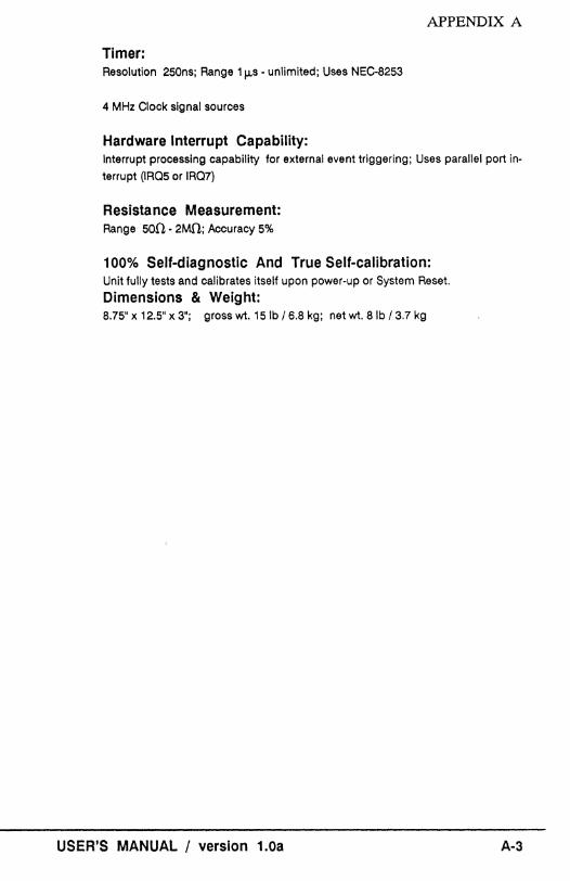
APPENDIX A
Timer: Resolution 250ns; Range 1 f.Ls - unlimited; Uses NEC-S253
4 MHz Clock signal sources
Hardware Interrupt Capability: Interrupt processing capability for external event triggering; Uses parallel port in
terrupt (IRQ5 or IRQ7)
Resistance Measurement: Range 500 - 2Mfi; Accuracy 5%
100% Self-diagnostic And True Self-calibration: Unit fully tests and calibrates itself upon power-up or System Reset.
Dimensions & Weight: S.75" x 12.5" x 3"; gross wt. 151b / 6.S kg; net wt. Sib / 3.7 kg
USER'S MANUAL / version 1.0a A-3

APPENDIX A
This page left blank intentionally.
A-4 USER'S MANUAL / version 1.0a
APPENDIX B PROTEUS MESSAGES
ADEL MESSAGES
USER'S MANUAL I version 1.0a
APPENDIXB
B-1
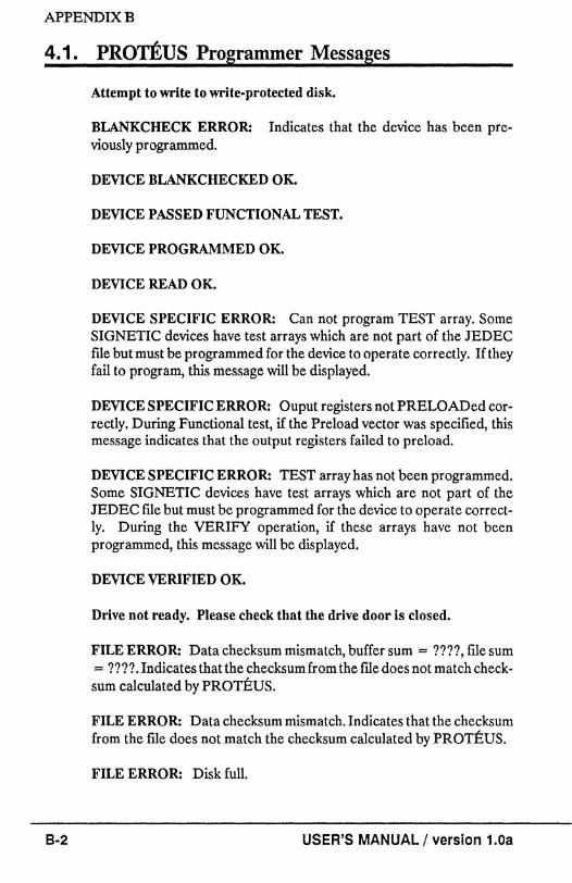
APPENDIXB
4.1. PROTEUS Programmer Messages
B·2
Attempt to write to write-protected disk.
BLANKCHECK ERROR! Indicates that the device has been previously programmed.
DEVICE BLANKCHECKED OK.
DEVICE PASSED FUNCTIONAL TEST.
DEVICE PROGRAMMED OK.
DEVICE READ OK.
DEVICE SPECIFIC ERROR: Can not program TEST array. Some SIGNETIC devices have test arrays which are not part of the JEDEC me but must be programmed for the device to operate correctly. If they fail to program, this message will be displayed.
DEVICE SPECIFIC ERROR: Ouput registers not PRELOADed correctly. During Functional test, if the Preload vector was specified, this message indicates that the output registers failed to preload.
DEVICE SPECIFIC ERROR: TEST array has not been programmed. Some SIGNETIC devices have test arrays which are not part of the JEDEC file but must be programmed for the device to operate correctly. During the VERIFY operation, if these arrays have not been programmed, this message will be displayed.
DEVICE VERIFIED OK.
Drive not ready. Please check that the drive door is closed.
FILE ERROR! Data checksum mismatch, buffer sum = ????, file sum = ???? Indicates that the checksum from the file does not match checksum calculated by PROTEUS.
FILE ERROR! Data checksum mismatch. Indicates that the checksum from the file does not match the checksum calculated by PROTEUS.
FILE ERROR: Disk full.
USER'S MANUAL / version 1.0a
APPENDIXB
FILE ERROR: File or pathname not found.
FILE ERROR: No fIles found.
FILE ERROR: Some records are out of range and not loaded. During the 'Load fIle' operation, if some records were out of the range for the From address and Blocksize, then this message will be displayed.
FILE ERROR: System fIle names are illegal. When loading or saving a fIle, system fIles may not be specified. System files are PROTEUS. *, SYS. *, and USER. *.
FILE ERROR: Unexpected end of file reached. Some fIle formats have an end of file marker. During the 'Load file' operation, this message will be displayed, if the end of fIle is reached before the end of file marker is found.
FILE LOADED OK.
FILE SAVED OK.
HARDWARE ERROR: CAP %i stuck on %s. HARDWARE ERROR: Could not calibrate DAC %i (%f). HARDWARE ERROR: Could not calibrate DAC trimmer. HARDWARE ERROR: pin ## VPPI driver ???V, +-???V).HARDWAREERROR: pin ## VPPI driver?? .?V. HARDWARE ERROR: TTL driver pin??, stuck on ?? HARDWARE TIMER ERROR. Indicates that the unit needs repair or that the host computer is not compatible. If these messages persist, contact B&C Microsystem's service department.
No test vectors to execute. Please create some.
OPERATION ABORTED BY USER.
OPERATION COMPLETE. Checksum = ????
OVER-CURRENT FAULT: May be display during programming operations and may indicate that the device in the socket is bad.
PROGRAM ERROR at ???? Hex Device data =???? Buffer data = nn SEEK error. Please check that drive is connected properly. SORRY. Register PRELOAD not supported for this device. TEST ERROR: Vector n, Pin n, Test code = H, pin voltage = ???? Unkown drive error, please check your workstation.
USER'S MANUAL I version 1.0a B-3

APPENDIXB
8-4
USER ERROR: ASCII mode not allowed with 4-bit device. Since the ASCII code requires 8-bits, the ASCII mode is not allowed during 'Edit buffer data' operation if selected device's data bus is only 4-bits.
USER ERROR: Device does not support this feature.
USER ERROR: Illegal key pressed.
USER ERROR: Illegal parameter entered.
USER ERROR: JEDEC format must be selected for logic devices. JEDEC format is the only legal file translation format for logic devices.
USER ERROR: A logic device must be selected for JEDEC translation. JEDEC format may not be selected if a memory devices has been selected.
USER ERROR: ManufacturerlPart # not found.
USER ERROR: Parameters out of range.
USER ERROR: Proprietary information, please select USER library. Due to obligations to the device manufacturers, we are not permitted to show you programming algorithms for each device. However, we have provided a USER device library which contains sample programming algorithms, for most types of devices, which may be modified andior added upon as needed. If you wish to view these algorithms, please go to the OPTIONS screen and select the USER library first.
USER ERROR: String not found.
USER ERROR: Uninitialized fuse cell may not be edited.
VERFIY ERROR at ???? Hex Device data = ???? Buffer data = nn
ADEL Messages
COMPILER LIMIT: Argument too complex. Indicates that the equation is too complex. To get around this problem, split the equation into two seperate equations.
USER'S MANUAL / version 1.0a

APPENDIXB
COMPILER LIMIT: Macro name table full. Too many macros have been defmed.
COMPILER LIMIT: Macro string queue full. Too many macros have been defmed.
COMPILER LIMIT: String literal too large. In ADEL strings are limited to a maximum of 100 characters. However this error often occurs when the closing quotation mark has been left out.
COMPILER LIMIT: Symbol table overflow. Too many variables have been defmed.
COMPILER LIMIT: Too many active loops. Too many 'while' statements.
COMPILER LIMIT: Too many arguments in CALL. The limit on the number of arguments that may be passed to another function has been reached.
CROSS REFERENCE ERROR: Argument not defined in parameter list.
SYNTAX ERROR: All rows must have equal length. In the '#hvtable' directive, all rows must be the same number of entries.
SYNTAX ERROR: Expecting 'shift register length'. In the 'sput', 'sget', and 'sputentry' commands this message will be displayed if the 'shift register length' parameter is not specified.
SYNTAX ERROR: Expecting variable definition.
SYNTAX ERROR: Illegal argument name.
SYNTAX ERROR: Illegal array size.
SYNTAX ERROR: Illegal dbase ID. Legal dbase IDs are PIN, FAM, DMP, TAB, and WA V.
SYNTAX ERROR: Illegal macro name.
SYNTAX ERROR: Illegal number of arguments.
SYNTAX ERROR: Illegal number of parameters.
USER'S MANUAL / version 1.0a 8-5

APPENDIXB
8-6
SYNTAX ERROR: Illegal parameter.
SYNTAX ERROR: Illegal pattern ID. When defining a device fuse map conversion sequence you have specified an unkown variable.
SYNTAX ERROR: Illegal record number.
SYNTAX ERROR: Illegal symbol name.
SYNTAX ERROR: Illegal variable name.
SYNTAX ERROR: Missing '('.
SYNTAX ERROR: Missing ')'.
SYNTAX ERROR: Missing ';'
SYNTAX ERROR: Missing ']'
SYNTAX ERROR: Missing comma.
SYNTAX ERROR: Missing final '}'.
SYNTAX ERROR: Out oflocal symbol space. Too many local symbols were defined.
SYNTAX ERROR: Symbol already defined. Variables may not be defined with the same name twice.
SYNTAX ERROR: Unexpected end of record reached.
SYNTAX ERROR: Unexpected end of table reached.
USER ERROR: Cursor must be at rec# argument of '#load' command to zoom.
USER ERROR: Cursor must be at record # field to zoom.
USER ERROR: Device map record # out of range. You have specified a device fuse map record that does not exists.
USER ERROR: Family record # out of range. You have specified a family record that does not exists.
USER'S MANUAL / version 1.0a

APPENDIXB
USER ERROR: Pin configuration record # out of range. You have specified a pin configuration record that does not exists.
USER ERROR: Record does not exists.
USER'S MANUAL / version 1.0a B-7

APPENDIXB
This page left blank intentionally.
8-8 USER'S MANUAL / version 1.0a

APPENDIX C
APPENDIX C LIST OF PROGRAMMABLE DEVICES
USER'S MANUAL / version 1.0a C-1

APPENDIX C
This page left blank intentionally.
C-2 USER'S MANUAL / version 1.0a


![Proteus All-In-One Manual v6[1]_3(1)](https://img.pdfslide.us/doc/110x75/55cf9ac6550346d033a35713/proteus-all-in-one-manual-v6131.jpg)