Embed Size (px)
Citation preview

TABLE OF CONTENTS
Paragraph PageNumber Title Number
Date: 8-20-98Revision No: 0.1Pages affected: see change bars
F
ree
sca
le S
em
ico
nd
uc
tor,
I
Freescale Semiconductor, Inc.n
c..
.
Section 1
Section 2Introduction
2.1 Background ..........................................................................................1-12.2 MCF5204 Features ..............................................................................1-22.3 Overview ..............................................................................................1-32.3.1 ColdFire Processor Core ............................................................1-42.4 Processor States ..................................................................................1-42.5 Programming Model .............................................................................1-42.6 Data Format Summary .........................................................................1-72.7 Addressing Capabilities Summary .......................................................1-72.8 Notational Conventions ........................................................................1-92.9 Instruction Set Overview ....................................................................1-122.9.1 Instruction Cache .....................................................................1-142.9.2 Internal SRAM ..........................................................................1-142.9.3 UART Module ...........................................................................1-142.9.4 Timers ......................................................................................1-142.9.5 System Interface Module (SIM) ................................................1-152.9.5.1 External Bus Interface. .................................................1-152.9.5.2 Chip-Selects. ................................................................1-152.9.5.3 8-Bit General Purpose I/O Interface. ............................1-152.9.5.4 Interrupt Controller. .......................................................1-152.9.5.5 System Protection. ........................................................1-152.9.5.6 JTAG. ............................................................................1-152.9.6 System Debug Interface ...........................................................1-152.9.7 Power Management .................................................................1-162.9.8 Pinout and Package .................................................................1-16
Section 3Signal Descriptions
3.1 Signals Overview ..................................................................................2-13.1.1 Signal Index Field Definitions .....................................................2-23.2 Signal Index ..........................................................................................2-33.3 Signal Definitions ..................................................................................2-43.3.1 External Bus Signals ..................................................................2-4
MOTOROLA MCF5204 USER’S MANUAL vii For More Information On This Product,
Go to: www.freescale.com

TABLE OF CONTENTS (Continued)
Paragraph PageNumber Title Number
F
ree
sca
le S
em
ico
nd
uc
tor,
I
Freescale Semiconductor, Inc.n
c..
.
3.3.1.1 Address Bus (A[21:20])/(PP[1:0]) ................................... 2-43.3.1.2 Address Bus (A[19:0]) .................................................... 2-43.3.1.3 Data Bus (D[15:0]) .......................................................... 2-43.3.2 Bus Control ................................................................................ 2-43.3.2.1 Data Transfer Acknowledge DTACK .............................. 2-43.3.2.2 Read Enable (RE) .......................................................... 2-43.3.2.3 Write Enable (WE) .......................................................... 2-53.3.2.4 Upper/Lower Write Enable (UWE/LWE).......................... 2-53.3.2.5 Bus Width (BUSW/ATS) ................................................. 2-63.3.3 Exception Control Signals .......................................................... 2-63.3.3.1 Reset (RESET) ............................................................... 2-63.3.4 Chip-select Signals .................................................................... 2-63.3.4.1 Chip-Selects (CS[5:0]) .................................................... 2-63.3.5 Interrupt Request Signals (IRQ[3:0]) .......................................... 2-73.3.6 Clock Signals (CLK) ................................................................... 2-73.3.7 Timer Signals ............................................................................. 2-73.3.7.1 Timer Input (TIN/PP2) .................................................... 2-73.3.7.2 Timer Output (TOUT/PP3) .............................................. 2-73.3.8 Serial Signals ............................................................................. 2-73.3.8.1 Transmit Data (TXD/PP4) ............................................... 2-73.3.8.2 Receive Data (RXD/PP5) ............................................... 2-73.3.8.3 Clear To Send (CTS/PP6) .............................................. 2-83.3.8.4 Request To Send (RTS/PP7) ......................................... 2-83.3.9 Test and Debug Signals ............................................................. 2-83.3.9.1 MTMOD .......................................................................... 2-83.3.9.2 Break Point (BKPT/TMS) ................................................ 2-83.3.9.3 Debug Serial data Input DSI/TDI) ................................... 2-83.3.9.4 Debug Serial data Output (DSO/TDO) ........................... 2-93.3.9.5 Debug Serial Clock DSCLK (TRST) ............................... 2-93.3.9.6 JTAG Clock (TCLK) ...................................................... 2-103.3.9.7 Debug Data (DDATA[3:0]) ........................................... 2-103.3.9.8 Processor Status (PST/hiz[3:0]) ................................... 2-10
Section 4ColdFire Core
4.1 Processor Pipelines ............................................................................. 3-14.2 Processor Register Description ............................................................ 3-24.2.1 User Programming Model .......................................................... 3-24.2.1.1 Data Registers (D0–D7) ................................................. 3-24.2.1.2 Address Registers (A0–A6) ............................................ 3-24.2.1.3 Stack Pointer (A7) .......................................................... 3-2
viii MCF5204 USER’S MANUAL MOTOROLA For More Information On This Product,
Go to: www.freescale.com
TABLE OF CONTENTS (Continued)
Paragraph PageNumber Title Number
F
ree
sca
le S
em
ico
nd
uc
tor,
I
Freescale Semiconductor, Inc.n
c..
.
4.2.1.4 Program Counter ............................................................3-24.2.1.5 Condition Code Register .................................................3-34.2.2 Supervisor Programming Model .................................................3-44.2.2.1 Status Register ...............................................................3-44.2.2.2 Vector Base Register (VBR) ...........................................3-54.3 Exception Processing Overview ...........................................................3-54.4 Exception Stack Frame Definition ........................................................3-74.5 Processor Exceptions ...........................................................................3-84.5.1 Access Error Exception ..............................................................3-84.5.2 Address-Error Exception ............................................................3-94.5.3 Illegal Instruction Exception ........................................................3-94.5.4 Privilege Violation .......................................................................3-94.5.5 Trace Exception .......................................................................3-104.5.6 Debug Interrupt ........................................................................3-104.5.7 RTE and Format Error Exceptions ...........................................3-104.5.8 TRAP Instruction Exceptions ....................................................3-114.5.9 Interrupt Exception ...................................................................3-114.5.10 Fault-on-Fault Halt ....................................................................3-114.5.11 Reset Exception .......................................................................3-114.6 Instruction Execution Timing ..............................................................3-114.6.1 Timing Assumptions .................................................................3-124.6.2 MOVE Instruction Execution Times ..........................................3-13
Section 5Instruction Cache
5.1 Features of Instruction Cache ..............................................................4-15.2 Instruction cache Physical Organization ..............................................4-15.3 Instruction cache Operation .................................................................4-25.3.1 Interaction With Other Modules ..................................................4-35.3.2 Memory Reference Attributes .....................................................4-35.3.3 Cache Coherency and Invalidation ............................................4-35.3.4 RESET .......................................................................................4-45.3.5 Cache Miss Fetch Algorithm/Line Fills .......................................4-45.4 Instruction Cache Programming Model ................................................4-55.4.1 Cache Control Register (CACR) ................................................4-55.4.1.1 Bit Definitions ..................................................................4-65.4.1.1.1 CENB - Cache Enable ................................................................4-65.4.1.1.2 CPDI - Disable CPUSHL Invalidation .........................................4-65.4.1.2 CFRZ - Cache Freeze ....................................................4-65.4.1.3 CINV - Cache Invalidate .................................................4-75.4.1.4 CEIB - Cache Enable Instruction Bursting...................... 4-7
MOTOROLA MCF5204 USER’S MANUAL ix For More Information On This Product,
Go to: www.freescale.com

TABLE OF CONTENTS (Continued)
Paragraph PageNumber Title Number
F
ree
sca
le S
em
ico
nd
uc
tor,
I
Freescale Semiconductor, Inc.n
c..
.
5.4.1.5 DCM - Default Cache Mode ........................................... 4-75.4.1.6 DBWE - Default Buffered Write Enable .......................... 4-75.4.1.7 DWP - Default Write Protection ...................................... 4-75.4.1.8 CLNF[1:0] - Cache Line Fill ............................................ 4-85.5 Access Control Registers ..................................................................... 4-85.6 Features ............................................................................................... 4-85.7 ACR Programming Model .................................................................... 4-85.7.1 Access Control Registers (ACR0, ACR1) .................................. 4-85.7.1.1 AB[31:24] - Address Base [31:24] .................................. 4-95.7.1.2 AM[23:16] - Address Mask [23:16] ................................. 4-95.7.1.3 EN - Enable .................................................................... 4-95.7.1.4 SM[1:0] - Supervisor mode ............................................. 4-95.7.1.5 CM - Cache Mode .......................................................... 4-95.7.1.6 BWE- Buffered Write Enable .......................................... 4-95.7.1.7 WP - Write Protect ........................................................ 4-10
Section 6SRAM
6.1 SRAM Features .................................................................................... 5-16.2 SRAM Operation .................................................................................. 5-16.3 SRAM Programming Model ................................................................. 5-16.3.1 SRAM Base Address Register ................................................... 5-26.3.1.1 BA[31:0] - Base Address ............................................... 5-26.3.1.2 WP - Write Protect ......................................................... 5-26.3.1.3 AS[5:1] - Address Space Masks .................................... 5-26.3.1.4 V - Valid ......................................................................... 5-36.3.2 SRAM Initialization ..................................................................... 5-36.3.3 Power Management ................................................................... 5-3
Section 7Bus Operation
7.1 Bus And Control Signals ...................................................................... 6-17.1.1 Address Bus ............................................................................... 6-17.1.2 Data Bus .................................................................................... 6-17.1.3 Chip Select ................................................................................. 6-17.1.4 ATS ............................................................................................ 6-17.1.5 RE - Read Enable ...................................................................... 6-27.1.6 WE - Write Enable ...................................................................... 6-27.1.7 Byte Write Enables/Byte Data Strobes ...................................... 6-27.1.7.1 Byte Write Enable Mode ................................................. 6-2
x MCF5204 USER’S MANUAL MOTOROLA For More Information On This Product,
Go to: www.freescale.com

TABLE OF CONTENTS (Continued)
Paragraph PageNumber Title Number
F
ree
sca
le S
em
ico
nd
uc
tor,
I
Freescale Semiconductor, Inc.n
c..
.
7.1.7.2 Byte Data Strobe Mode ..................................................6-27.1.7.3 Byte Enable Operation ....................................................6-27.1.8 DTACK .......................................................................................6-37.2 Direct Connection Bus Interface ...........................................................6-37.3 Wait States ...........................................................................................6-37.4 Port Sizing ............................................................................................6-47.5 Bursting Operation ...............................................................................6-47.6 Bus Exceptions .....................................................................................6-47.6.1 IACK ...........................................................................................6-47.6.2 Bus Errors ..................................................................................6-47.6.3 Halt .............................................................................................6-47.6.4 Double Bus Fault ........................................................................6-57.7 Bus Characteristics ..............................................................................6-57.8 Read and Write Cycles With Internal Termination .............................6-117.8.1 IACK Cycles with Internal Termination .....................................6-337.8.2 IACK Cycle During Autovectored Response ............................6-357.9 RESET Operation ...............................................................................6-367.9.1 ATS Activation ..........................................................................6-367.9.2 BUSW Sample Time ................................................................6-36
Section 8System Integration Module (SIM)
8.1 System Integration Module (SIM) Introduction .....................................7-18.2 SIM Operation ......................................................................................7-28.2.1 Module Base Address Register ..................................................7-28.2.2 Chip Select Operation ................................................................7-28.2.2.1 Programmable Features .................................................7-28.2.2.2 Global Chip Select Operation. ........................................7-28.2.2.3 Normal Chip Select Operation ........................................7-38.2.2.3.1 Chip Select Prioritization ............................................................7-38.2.2.3.2 Chip Select Used for IACK Indication .........................................7-38.2.3 Bus Timeout Monitor ..................................................................7-38.2.4 Spurious Interrupt Monitor ..........................................................7-38.2.5 Software Watchdog Timer (SWT) ..............................................7-48.2.6 Interrupt Controller .....................................................................7-58.2.7 Reset operation ..........................................................................7-68.3 Programming Model .............................................................................7-68.3.1 SIM Registers Memory Map .......................................................7-68.3.2 Memory Map ..............................................................................7-78.3.3 SIM Registers .............................................................................7-88.3.3.1 Module BASE Address Register (MBAR) .......................7-8
MOTOROLA MCF5204 USER’S MANUAL xi For More Information On This Product,
Go to: www.freescale.com

TABLE OF CONTENTS (Continued)
Paragraph PageNumber Title Number
F
ree
sca
le S
em
ico
nd
uc
tor,
I
Freescale Semiconductor, Inc.n
c..
.
8.3.3.1.1 BA[31:9] - Base Address ............................................................ 7-98.3.3.1.2 C/I,SC,SD,UC,UD - Address Space Masks ............................... 7-98.3.3.1.3 V - Valid ...................................................................................... 7-98.3.3.2 SIM Configuration Register (SIMR) ................................ 7-98.3.3.2.1 FRZ1 - Freeze Software Watchdog Timer Enable ..................... 7-98.3.3.2.2 FRZ0 - Freeze Bus Monitor Enable ........................................... 7-98.3.3.3 Interrupt Control Register (ICR_xX) ............................. 7-108.3.3.3.1 AVEC - Autovector Enable ....................................................... 7-108.3.3.3.2 IL2-IL0 - Interrupt Level ............................................................ 7-108.3.3.3.3 IP1-IP0 - Interrupt Priority ........................................................ 7-108.3.3.4 Interrupt Mask register (IMR) ........................................ 7-118.3.3.4.1 IMK - Interrupt Mask ................................................................. 7-118.3.3.5 Interrupt Pending Register (IPR) .................................. 7-128.3.3.5.1 IPN - Interrupt Pending ............................................................ 7-128.3.3.6 Reset Status Register (RSR) ........................................ 7-138.3.3.6.1 HRST - Hard Reset or System Reset ...................................... 7-138.3.3.6.2 SWTR - Software Watchdog Timer Reset ............................... 7-138.3.3.7 System Protection Control Register (SYPCR) .............. 7-138.3.3.7.1 SWE - Software Watchdog Enable .......................................... 7-138.3.3.7.2 SWRI - Software Watchdog Reset/Interrupt Select ................. 7-148.3.3.7.3 SWP - Software Watchdog Prescaler ...................................... 7-148.3.3.7.4 SWT1-SWT0 - Software Watchdog Timing .............................. 7-148.3.3.7.5 BME - Bus Monitor External Enable ......................................... 7-148.3.3.7.6 BMT1-BMT0 - Bus Monitor Timing ........................................... 7-158.3.3.8 Software Watchdog Interrupt Vector Register (SWIVR) 7-158.3.3.9 Software Watchdog Service Register (SWSR) ............. 7-158.3.4 Chip-Select Registers .............................................................. 7-168.3.4.1 Chip-Select Base Address Register (CSARX) ............. 7-168.3.4.1.1 BA[21:8]: Base Address Bits ................................................... 7-168.3.4.2 Chip-Select address mask register (CSMRX) .............. 7-178.3.4.2.1 BAM[31:9]: Address Mask Bits ................................................. 7-178.3.4.2.2 WP: Write Protect ..................................................................... 7-178.3.4.2.3 C/I,SC,SD,UC,UD - Address Space Masks ............................. 7-178.3.5 Chip Select Control Register (CSCRx) .................................... 7-188.3.5.1 WS[2:0]- Wait States .................................................... 7-188.3.5.2 AA - Auto Acknowledge Enable .................................... 7-188.3.5.3 PS: Port Size ................................................................ 7-188.3.5.4 BRST - Burst Enable .................................................... 7-188.3.5.5 BEM: Byte Mode Enable .............................................. 7-198.3.5.6 V: Valid Bit .................................................................... 7-198.4 General-Purpose I/O Port (Port A) Configuration Registers .............. 7-208.4.1 Pin Assignment Register (PAR) ............................................... 7-20
xii MCF5204 USER’S MANUAL MOTOROLA For More Information On This Product,
Go to: www.freescale.com

TABLE OF CONTENTS (Continued)
Paragraph PageNumber Title Number
F
ree
sca
le S
em
ico
nd
uc
tor,
I
Freescale Semiconductor, Inc.n
c..
.
8.4.1.1 Port A Data Direction Register (PADDR) ......................7-218.4.1.2 Port A Data Register (PADAT) ......................................7-21
Section 9UART Module
9.1 Module Overview ..................................................................................8-29.1.1 Serial Communication Channel ..................................................8-29.1.2 Baud-Rate Generator/Timer .......................................................8-39.1.3 Interrupt Control Logic ................................................................8-39.2 UART Module Signal Definitions ..........................................................8-39.2.1 Transmitter Serial Data Output (TxD) .........................................8-39.2.2 Receiver Serial Data Input (RxD) ...............................................8-49.2.3 Request-To-Send (RTS) ............................................................8-49.2.4 Clear-To-Send (CTS) .................................................................8-49.3 Operation ..............................................................................................8-59.3.1 Baud-Rate Generator/Timer .......................................................8-59.3.2 Transmitter and Receiver Operating Modes ..............................8-59.3.2.1 Transmitter ......................................................................8-69.3.2.2 Receiver ..........................................................................8-99.3.2.3 FIFO Stack ....................................................................8-119.3.3 Looping Modes .........................................................................8-129.3.3.1 Automatic Echo Mode ...................................................8-129.3.3.2 Local Loopback Mode ...................................................8-129.3.3.3 Remote Loopback Mode ...............................................8-139.3.4 Multidrop Mode .........................................................................8-149.3.5 Bus Operation ..........................................................................8-169.3.5.1 Read Cycles .................................................................8-169.3.5.2 Write Cycles ..................................................................8-169.3.5.3 Interrupt Acknowledge Cycles ......................................8-169.4 Register Description and Programming .............................................8-169.4.1 Register Description .................................................................8-169.4.1.1 Mode Register 1 (UMR1) ..............................................8-179.4.1.2 Mode Register 2 (UMR2) ..............................................8-199.4.1.3 Status Register (USR) ..................................................8-219.4.1.4 Clock-Select Register (UCSR) ......................................8-249.4.1.5 Command Register (UCR) ............................................8-249.4.1.6 Receiver Buffer (URB) ..................................................8-279.4.1.7 Transmitter Buffer (UTB) ..............................................8-289.4.1.8 Input Port Change Register (UIPCR) ............................8-289.4.1.9 Auxiliary Control Register (UACR) ................................8-299.4.1.10 Interrupt Status Register (UISR) ...................................8-29
MOTOROLA MCF5204 USER’S MANUAL xiii For More Information On This Product,
Go to: www.freescale.com

TABLE OF CONTENTS (Continued)
Paragraph PageNumber Title Number
F
ree
sca
le S
em
ico
nd
uc
tor,
I
Freescale Semiconductor, Inc.n
c..
.
9.4.1.11 Interrupt Mask Register (UIMR) .................................... 8-309.4.1.12 Timer Upper Preload Register (UBG1) ......................... 8-329.4.1.13 Timer Lower Preload Register (UBG2) ......................... 8-329.4.1.14 Interrupt Vector Register (UIVR) .................................. 8-329.4.1.15 Output Port Data Registers (UOP1, UOP0) ................. 8-339.4.2 Programming ............................................................................ 8-339.4.2.1 UART Module Initialization ........................................... 8-349.4.2.2 I/O Driver Example ....................................................... 8-349.4.2.3 Interrupt Handling ......................................................... 8-349.5 UART Module Initialization Sequence ................................................ 8-34
Section 10Timer Module
10.1 Overview .............................................................................................. 9-110.1.1 Key Features .............................................................................. 9-110.2 Module Operation ................................................................................. 9-210.2.1 General Purpose Timer Units ..................................................... 9-210.2.1.1 Prescaler ........................................................................ 9-310.2.1.2 Capture Mode ................................................................. 9-310.2.1.3 Reference Compare ....................................................... 9-310.2.1.4 Output Mode ................................................................... 9-310.3 Programming Model ............................................................................. 9-310.3.1 General Purpose Timer Registers .............................................. 9-310.3.1.1 Timer Mode Register (TMR) ........................................... 9-410.3.1.2 Timer Reference Register (TRR) .................................... 9-510.3.1.3 Timer Capture Register (TCR) ....................................... 9-510.3.1.4 Timer Counter (TCN) ...................................................... 9-510.3.1.5 Timer Event Register (TER) ........................................... 9-6
Section 11Debug Support
11.1 Real-Time Trace ................................................................................ 10-111.2 Background Debug Mode (BDM) ....................................................... 10-411.2.1 CPU Halt .................................................................................. 10-511.2.2 BDM Serial Interface ................................................................ 10-611.2.3 BDM Command Set ................................................................. 10-711.2.3.1 BDM Command Set Summary ..................................... 10-711.2.3.2 ColdFire BDM Commands ............................................ 10-811.2.3.3 Command Sequence Diagram ..................................... 10-911.2.3.4 Command Set Descriptions ........................................ 10-10
xiv MCF5204 USER’S MANUAL MOTOROLA For More Information On This Product,
Go to: www.freescale.com
TABLE OF CONTENTS (Continued)
Paragraph PageNumber Title Number
F
ree
sca
le S
em
ico
nd
uc
tor,
I
Freescale Semiconductor, Inc.n
c..
.
11.2.3.4.1 Read A/D Register (RAREG/RDREG) ...................................10-1011.2.3.4.2 Write A/D Register (WAREG/WDREG) ..................................10-1111.2.3.4.3 Read Memory Location (READ) .............................................10-1211.2.3.4.4 Write Memory Location (WRITE) ...........................................10-1411.2.3.4.5 Dump Memory Block (DUMP) ................................................10-1611.2.3.4.6 Fill Memory Block (FILL) ........................................................10-1811.2.3.4.7 Resume Execution (GO) ........................................................10-2011.2.3.4.8 No Operation (NOP) ...............................................................10-2011.2.3.4.9 Read Control Register (RCREG) ...........................................10-2111.2.3.4.10 Write Control Register (WCREG) ...........................................10-2211.2.3.4.11 Read Debug Module Register (RDMREG) .............................10-2311.2.3.4.12 Write Debug Module Register (WDMREG) ............................10-2311.2.3.4.13 Unassigned Opcodes .............................................................10-2411.3 Real-Time Debug Support ................................................................10-2511.3.1 Programming Model ...............................................................10-2511.3.1.1 Address Breakpoint Registers (ABLR, ABHR) ...........10-2611.3.1.2 Address Attribute Breakpoint Register (AATR) ...........10-2611.3.1.3 Program Counter Breakpoint Register (PBR, PBMR) 10-2811.3.1.4 Data Breakpoint Register (DBR, DBMR) ....................10-2811.3.1.5 Trigger Definition Register (TDR) ...............................10-2911.3.1.6 Configuration/Status Register (CSR) ..........................10-3111.3.2 Theory of Operation ...............................................................10-3311.3.2.1 Reuse Of Debug Module Hardware. ...........................10-3511.3.3 Concurrent BDM and Processor Operation ............................10-3511.4 Motorola Recommended BDM Pinout ..............................................10-3611.4.1 Differences Between the ColdFire BDM and a CPU32 BDM .10-36
Section 12JTAG Specification
12.1 1149.1 Standard JTAG Specification ..................................................11-112.2 Overview ............................................................................................11-212.3 JTAG Register Description ................................................................11-512.3.1 JTAG Instruction Shift Register ...............................................11-512.3.1.1 EXTEST Instruction .....................................................11-512.3.1.2 SAMPLE/PRELOAD Instruction ..................................11-512.3.1.3 HIGHZ Instruction ........................................................11-612.3.1.4 CLAMP Instruction .......................................................11-612.3.1.5 BYPASS Instruction .....................................................11-612.4 TAP Controller ....................................................................................11-712.4.1 JTAG Bypass Register .............................................................11-8
MOTOROLA MCF5204 USER’S MANUAL xv For More Information On This Product,
Go to: www.freescale.com

TABLE OF CONTENTS (Continued)
Paragraph PageNumber Title Number
F
ree
sca
le S
em
ico
nd
uc
tor,
I
Freescale Semiconductor, Inc.n
c..
.
Section 13Electrical Characteristics
13.1 Maximum Ratings .............................................................................. 12-113.2 Clock Input Specification ................................................................... 12-213.3 DC Electrical Specifications ............................................................... 12-313.4 AC Electrical Specification ................................................................. 12-313.4.1 Maximum Output Loading ........................................................ 12-313.4.2 Bus Timing ............................................................................... 12-313.4.2.1 Input Setup and Hold Waveform .................................. 12-413.4.2.2 Output Setup and Hold Waveform ................................ 12-513.5 Pin Timings ........................................................................................ 12-513.5.1 Reset Timing ............................................................................ 12-513.5.2 Interrupt Timing ....................................................................... 12-513.5.2.1 Reset Configuration Timing .......................................... 12-613.5.3 Activation of ATS ...................................................................... 12-613.5.4 BUSW Timing Diagram ............................................................ 12-713.6 Bus Timing Diagrams ......................................................................... 12-813.6.1 AC Debug Timing Specification ............................................. 12-1013.6.1.1 Debug Timing Diagrams ............................................. 12-1013.6.2 HIZ Timing Specification ......................................................... 12-1113.6.2.1 HIZ Timing Diagrams .................................................. 12-1113.6.3 Timer Timing .......................................................................... 12-1213.6.3.1 Timer AC Timing Diagrams and Specifications .......... 12-1213.6.3.2 Timer Timing Diagrams .............................................. 12-1213.6.4 UART Timing .......................................................................... 12-1313.6.4.1 UART Module AC Timing Specifications .................... 12-1313.6.4.2 UART Timing Diagrams .............................................. 12-1313.6.5 General-Purpose I/O Timing .................................................. 12-1413.6.5.1 General-Purpose I/O AC Timing Specifications ......... 12-1413.6.5.2 General-Purpose I/O Timing Diagrams ....................... 12-1413.6.5.3 Boundary scan Timing Diagrams ............................... 12-1413.6.6 IEEE 1149.1 (JTAG) Timing ................................................... 12-1513.6.6.1 IEEE 1149.1 AC Timing Specification ........................ 12-1513.6.6.2 Test Clock Timing Diagrams ....................................... 12-1513.6.6.3 Boundary Scan Timing Diagrams................................ 12-1613.6.6.4 Test Access Port Timing Diagrams ............................. 12-1613.6.7 MTMOD Timing....................................................................... 12-1713.6.7.1 MTMOD Timing Specification...................................... 12-1713.6.7.2 MTMOD Timing Diagram............................................. 12-17
xvi MCF5204 USER’S MANUAL MOTOROLA For More Information On This Product,
Go to: www.freescale.com

TABLE OF CONTENTS (Continued)
Paragraph PageNumber Title Number
F
ree
sca
le S
em
ico
nd
uc
tor,
I
Freescale Semiconductor, Inc.n
c..
.
Section 14Mechanical Characteristics
14.1 Ordering Information ..........................................................................13-114.2 Package ..............................................................................................13-214.3 Pin Out ...............................................................................................13-314.4 Pin Out ASCII ....................................................................................13-4
Appendix APorting from M68K Family Devices
0.1 C Compilers and Host Software .......................................................... A-10.2 Target Software Port ........................................................................... A-10.3 Initialization Code ................................................................................ A-20.4 Exception Handlers ............................................................................. A-20.5 Supervisor Registers ........................................................................... A-3A.5
A.1A.2A.3A.4
MOTOROLA MCF5204 USER’S MANUAL xvii For More Information On This Product,
Go to: www.freescale.com

TABLE OF CONTENTS (Continued)
Paragraph PageNumber Title Number
F
ree
sca
le S
em
ico
nd
uc
tor,
I
Freescale Semiconductor, Inc.n
c..
.
xviii MCF5204 USER’S MANUAL MOTOROLA For More Information On This Product,
Go to: www.freescale.com

LIST OF TABLES
Table PageNumber Title Number
Date: 8-20-98Revision No: 0.1Pages affected: See change bars
F
ree
sca
le S
em
ico
nd
uc
tor,
I
Freescale Semiconductor, Inc.n
c..
.
1-1. ColdFire MCF5204 Data Formats ................................................................... 1-71-2. ColdFire Effective Addressing Modes............................................................. 1-81-3. Specific Effective Addressing Modes.............................................................. 1-81-4. MOVE Specific Effective Addressing Modes .................................................. 1-81-5. Notational Conventions................................................................................... 1-91-6. Supervisor-Mode Instruction Summary......................................................... 1-122-1. Chip-Select Port Width.....................................................................................2-42-2. WE Control of Data Bus...................................................................................2-52-3. Data Strobe Control of Data Bus..................................................................... 2-52-4. PST Signal Encoding .................................................................................... 2-113-1. Exception Vector Assignments ....................................................................... 3-73-2. Format Field Encodings .................................................................................. 3-83-3. Fault Status Encodings ................................................................................... 3-83-4. Misaligned Operand References................................................................... 3-123-5. Move Byte and Word Execution Times......................................................... 3-133-6. Move Long Execution Times......................................................................... 3-133-7. One Operand Instruction Execution Time..................................................... 3-143-8. Two Operand Instruction Execution Times ................................................... 3-153-9. Miscellaneous Instruction Execution Times .................................................. 3-163-10. General Branch Instruction Execution Times................................................ 3-173-11. BRA, Bcc Instruction Execution Times.......................................................... 3-174-1. Initial Fetch Offset vs. CLNF Bits .................................................................... 4-44-2. Instruction Cache Operation as Defined by CACR[31,10] ..............................4-54-3. External Fetch Size Based on Miss Address and CLNF................................. 4-85-1. Examples of Typical RAMBAR Settings.......................................................... 5-47-1. CPU Registers Memory Map .......................................................................... 7-77-2. SIM Registers Memory Map............................................................................ 7-77-3. SWT Timeout ................................................................................................ 7-147-4. BMT Timeout .................................................................................................7-157-5. Wait State Encoding...................................................................................... 7-187-6. Byte Enable Mode......................................................................................... 7-197-7. PAR Pin Assignment .....................................................................................7-208-1. UART Module Programming Model ...............................................................8-178-2. PMx and PT Control Bits............................................................................... 8-198-3. B/Cx Control Bits........................................................................................... 8-198-4. CMx Control Bits ........................................................................................... 8-198-5. SBx Control Bits ............................................................................................ 8-218-6. RCSx Control Bits ......................................................................................... 8-24
MOTOROLA USER’S MANUAL xxi For More Information On This Product,
Go to: www.freescale.com

LIST OF TABLES (Continued)
Table PageNumber Title Number
F
ree
sca
le S
em
ico
nd
uc
tor,
I
Freescale Semiconductor, Inc.n
c..
.
8-7. TCSx Control Bits ......................................................................................... 8-248-8. MISCx Control Bits......................................................................................... 8-258-9. TCx Control Bits............................................................................................. 8-268-10. RCx Control Bits ............................................................................................ 8-279-1. Programming Model for Timers ...................................................................... 9-310-1. Processor PST Definition.............................................................................. 10-210-2. CPU-Generated Message Encoding............................................................. 10-710-3. BDM Command Summary............................................................................ 10-710-4. BDM Size Field Encoding ............................................................................. 10-810-5. Control Register Map.................................................................................. 10-2110-6. Definition of DRc Encoding - Read ............................................................. 10-2310-7. Definition of DRc Encoding - Write ............................................................. 10-2410-8. SZ Encodings.............................................................................................. 10-2710-9. Transfer Type Encodings............................................................................ 10-2710-10. Transfer Modifier Encodings for Normal Transfers ..................................... 10-2810-11. Transfer Modifier Encodings for Alternate Access Transfers...................... 10-2810-12. Core Address, Access Size, and Operand Location................................... 10-2910-13. DDATA, CSR[31:28] Breakpoint Response................................................ 10-3410-14. Shared BDM/Breakpoint Hardware............................................................. 10-3511-1. JTAG Pin Description.................................................................................... 11-411-2. JTAG Instructions ......................................................................................... 11-5
xxii MCF5204 USER’S MANUAL MOTOROLA For More Information On This Product,
Go to: www.freescale.com

LIST OF ILLUSTRATIONS
Figure PageNumber Title Number
Date : 8-20-98Revision No: 0.1Pages affected: see change bars
F
ree
sca
le S
em
ico
nd
uc
tor,
I
Freescale Semiconductor, Inc.n
c..
.
1-1. MCF5204 Block Diagram................................................................................. 1-31-2. Programming Model......................................................................................... 1-61-3. MCF5204 Pinout Block Diagram...................................................................... 2-12-1. Chip-Select Port Width..................................................................................... 2-43-1. ColdFire Processor Core Pipelines .................................................................. 3-13-2. User Programming Model .................................................................................3-3 3-3. Supervisor Programming Model....................................................................... 3-53-4. Status Register................................................................................................. 3-73-5. Exception Stack Frame Form........................................................................... 3-74-1. Instruction Cache Block Diagram .....................................................................4-26-1. Signal Relationships to CLK............................................................................. 6-56-2. Read: Word, Word Port, External Termination, 1 Wait State ........................... 6-76-3. Read: Word, Word Port, External Termination, 2 Wait States ......................... 6-86-4. Write: Word, Word Port, External Termination, 1 Wait State ........................... 6-96-5. Write: Word, Word Port, External Termination, 2 Wait States ....................... 6-106-6. Read: Word, Word Port, Internal Termination, 0 Wait States ........................ 6-116-7. Read: Word, Word Port, Internal Termination, 1 Wait State .......................... 6-126-8. Read: Word, Word Port, Internal Termination, 2 Wait States ........................ 6-136-9. Write: Word, Word Port, Internal Termination, 0 Wait States......................... 6-146-10. Write: Word, Word Port, Internal Termination, 1 Wait State .......................... 6-156-11. Write: Word, Word Port, Internal Termination, 2 Wait States......................... 6-166-12. Read: Byte, Word Port, Internal Termination, 0 Wait States.......................... 6-176-13. Write: Byte, Word Port, Internal Termination, 0 Wait States .......................... 6-186-14. Read/Write: Word, Word Port, Internal Termination, 0 Wait States ............... 6-196-15. Read: Word, Byte Port, Internal Termination, Burst-Inhibited,
0 Wait States................................................................................................. 6-206-16. Read: Word, Byte Port, Internal Termination, Burst-Inhibited,
1 Wait State ................................................................................................... 6-216-17. Read: Word, Byte Port, Internal Termination, Burst-Enabled,
0 Wait States.................................................................................................. 6-226-18. Read: Word, Byte Port, Internal Termination, Burst-Enabled,
1 Wait State ................................................................................................... 6-236-19. Write: Word, Byte Port, Internal Termination, 0 Wait States .......................... 6-246-20. Write: Word, Byte Port, Internal Termination, 1 Wait State............................ 6-256-21. Read: Line, Word Port, Internal Termination, Burst-Inhibited, 0 Wait States . 6-266-22. Read: Line, Word Port, Internal Termination, Burst Inhibited,
1 Wait State ................................................................................................... 6-276-23. Read: Line, Word Port, Internal Termination, Burst-Enabled,
MOTOROLA USER’S MANUAL xix For More Information On This Product,
Go to: www.freescale.com
LIST OF ILLUSTRATIONS (Continued)
Figure PageNumber Title Number
F
ree
sca
le S
em
ico
nd
uc
tor,
I
Freescale Semiconductor, Inc.n
c..
.
0 Wait States ................................................................................................. 6-286-24. Read: Line, Word Port, Internal Termination, Burst-Enabled,
1 Wait State ................................................................................................... 6-296-25. Write: Line, Word Port, Internal Termination, 0 Wait States .......................... 6-306-26. Write: Line, Word Port, Internal Termination, 1 Wait State ............................ 6-316-27. IACK: External Termination, 1 Wait State...................................................... 6-326-28. IACK: Internal Termination, 0 Wait States ..................................................... 6-336-29. IACK: Internal Termination, 1 Wait State ....................................................... 6-346-30. IACK: Autovector ........................................................................................... 6-356-31. Reset Operation............................................................................................. 6-368-1. UART Block Diagram....................................................................................... 8-18-2. External and Internal Interface Signals ............................................................ 8-48-3. Baud Generator Diagram................................................................................. 8-58-4. Transmitter and Receiver Functional Diagram ................................................ 8-78-5. Transmitter Timing Diagram ............................................................................ 8-88-6. Receiver Timing Diagram .............................................................................. 8-108-7. Looping Modes Functional Diagram .............................................................. 8-138-8. Multidrop Mode Timing Diagram.................................................................... 8-158-9. Serial Module Programming Flowchart (5 pages)........................................... 8-369-1. Timer Block Diagram ....................................................................................... 9-210-1. Processor/Debug Module Interface ............................................................... 10-110-2. Pipeline Timing Example - Debug Output...................................................... 10-310-3. BDM Signal Sampling.................................................................................... 10-610-4. Command Sequence Diagram..................................................................... 10-1010-5. Debug Programming Model ......................................................................... 10-2510-6. 26-pin Berg Connector Arranged 2x13 ........................................................ 10-3610-7. Serial Transfer Illustration............................................................................ 10-3711-1. JTAG Mode, JTAG Disabled .......................................................................... 11-211-2. Background Debug Mode, JTAG Disabled.................................................... 11-211-3. JTAG Test Logic Block Diagram.................................................................... 11-411-4. JTAG TAP Controller State Machine ............................................................. 11-812-1. Clock Input Timing .......................................................................................... 12-212-2. Write Cycle Timing (shown with one wait state) ............................................ 12-812-3. Read Cycle Timing Diagram (shown with one wait state inserted)................ 12-9
xx USER’S MANUAL MOTOROLA For More Information On This Product,
Go to: www.freescale.com

DATE: 08-21-98
REVISION NO: 0.1
PAGES AFFECTED: SEE CHANGE BARS
F
ree
sca
le S
em
ico
nd
uc
tor,
I
Freescale Semiconductor, Inc.n
c..
.
SECTION 1INTRODUCTION
1.1 BACKGROUNDThe MCF5204 integrated microprocessor combines a ColdFire processor core with peripheral functions such as a timer, serial interface, and system integration module (SIM). Designed for embedded control applications, the ColdFire core delivers enhanced performance while maintaining low system costs. To speed program execution, the on-chip instruction cache and SRAM provide one-cycle access to critical code and data. The MCF5204 processor greatly reduces the time required for system design and implementation by packaging common system functions on the chip itself and by providing a glueless interface to 8- and16-bit SRAM, ROM, and I/O devices.
The revolutionary ColdFire microprocessor architecture gives cost-sensitive, high-volume markets new levels of price and performance. Based on the concept of variable-length RISC technology, ColdFire combines the architectural simplicity of conventional 32-bit RISC with a memory-saving, variable-length instruction set. In defining the ColdFire architecture for embedded processing applications, Motorola incorporated RISC architecture for peak performance and a simplified version of the variable-length instruction set found in the M68000 Family for code density.
By using a variable-length instruction set architecture, embedded processor designers using ColdFire RISC processors will enjoy significant system-level advantages over conventional fixed-length RISC architectures. The denser binary code for ColdFire processors consumes less valuable memory than any available fixed-length instruction set RISC processor. This improved code density means using more efficient system memory for a given application, and using slower, less costly memory to help achieve a target performance level.
The integrated peripheral functions provide high performance and flexibility. The serial interface consist of a programmable full duplex UART. Two 16-bit general-purpose multimode timers are included, one of which has input and output signals. For system protection, the processor includes a programmable 16-bit software watchdog timer and several bus monitors. In addition, common system functions such as chip-selects, interrupt control, bus arbitration, and IEEE 1149.1 test (JTAG) support are included in the SIM.
A sophisticated debug interface supports both Background-Debug mode and real-time trace. This interface is common to all ColdFire-based processors and allows common emulator support across the entire ColdFire Family.
MOTOROLA MCF5204 USER’S MANUAL 1-1 For More Information On This Product,
Go to: www.freescale.com

Introduction
F
ree
sca
le S
em
ico
nd
uc
tor,
I
Freescale Semiconductor, Inc.n
c..
.
1.2 MCF5204 FEATURESThe primary features of the MCF5204 integrated processor include the following:
• ColdFire Processor Core
— Variable-length RISC— 32-bit internal address bus with up to 4 MBytes of off-chip linear address space— 16-bit data bus— 16 user-visible 32-bit wide registers— Supervisor / User modes for system protection— Vector base register to relocate exception-vector table— Optimized for high-level language constructs— 13.5 MIPS at 33 MHz using Dhrystone 2.1
• 512-Byte Direct-Mapped Instruction Cache
• 512-Byte On-Chip SRAM
— Provides one-cycle access to critical code and data
• Universal Synchronous/Asynchronous Receiver/Transmitter (UART)
— Full duplex operation— Modem control signals available (CTS, RTS)— Processor-interrupt capability
• Dual 16 Bit General-Purpose Multimode Timers
— 8-bit prescaler— Timer input and output pins (Timer 1 only)— 30ns resolution with 33 MHz system clock— Processor-interrupt capability
• System Interface
— Various operating modes (input/capture, output/compare, free run/restart)— Glueless bus interface to 8 and16-bit SRAM, ROM, and I/O devices— 6 programmable chip-select signals— Programmable wait states and port sizes— System protection
• 16-bit software watchdog timer with prescaler• Double bus fault monitor• Bus timeout monitor• Spurious interrupt monitor
— Programmable interrupt controller• Low interrupt latency (3 clocks minimum)• 4 external interrupt inputs• 4 internal interrupt sources• Programmable interrupt priority and autovector generator
1-2 MCF5204 USER’S MANUAL MOTOROLA For More Information On This Product,
Go to: www.freescale.com

Introduction
F
ree
sca
le S
em
ico
nd
uc
tor,
I
Freescale Semiconductor, Inc.n
c..
.
— IEEE 1149.1 test (JTAG) support— 8-Bit general-purpose I/O interface
• System Debug Support
— Real-time trace— Background debug interface
• Power-Saving Features
• Fully Static 5.0-Volt Operation
• 100 Pin TQFP Package
1.3 OVERVIEWFigure 1-1 is a block diagram of the MCF5204 processor. The paragraphs that follow provide an overview of the integrated processor.
Figure 1-1. MCF5204 Block Diagram
SYSTEM
CHIP
INTERRUPT
PROTECTION
EXTERNAL
CHIP
SELECTS
INTERRUPT
SUPPORT
SERIAL
INTERFACE
CLOCK
INPUT
TIMER SUPPORT
BDM
INTERFACE
BUS INTERFACE
CONTROLLER
SELECTS
UART
TIMER1
512 BYTE ICACHE
COLDFIRE
512 BYTE SRAM
CORE
JTAG
SYST
EM B
US
CO
NTR
OLL
ERJTAG
INTERFACE
CLOCK
EXTERNAL
BUS
TIMER2
MOTOROLA MCF5204 USER’S MANUAL 1-3 For More Information On This Product,
Go to: www.freescale.com

Introduction
F
ree
sca
le S
em
ico
nd
uc
tor,
I
Freescale Semiconductor, Inc.n
c..
.
1.3.1 ColdFire Processor Core
The ColdFire processor core consists of two independent, decoupled pipeline structures to maximize performance while minimizing core size.The instruction fetch pipeline (IFP) is a two-stage pipeline for prefetching instructions. The prefetched instruction stream is gated into the two-stage operand execution pipeline (OEP), which decodes the instruction, fetches the required operands, and then executes the required function. Because the IFP and OEP pipelines are decoupled by an instruction buffer that serves as a FIFO queue, the IFP can prefetch instructions in advance of their actual use by the OEP, thereby minimizing time stalled waiting for instructions. The OEP is implemented in a two-stage pipeline featuring a traditional RISC data path with a dual read-ported register file feeding an arithmetic/logic unit.
1.4 PROCESSOR STATESThe processor is always in one of four states: normal processing, exception processing, stopped, or halted. It is in the normal processing state when executing instructions, fetching instructions and operands, and storing instruction results.
Exception processing is the transition from program processing to system, interrupt, and exception handling. Exception processing includes fetching the exception vector, stacking operations, and refilling the instruction fetch pipe after an exception. The processor enters exception processing when an exceptional internal condition arises, such as tracing an instruction, an instruction resulting in a trap, or executing specific instructions. External conditions, such as interrupts and access errors, also cause exceptions. Exception processing ends when the first instruction of the exception handler enters the operand execution pipeline.
Stopped mode is a reduced power operation mode that causes the processor to remain quiescent until either a reset or nonmasked interrupt occurs. The STOP instruction is used to enter this operational mode.
The processor halts when it receives an access error or generates an address error while in the exception processing state. For example, if during exception processing of one access error another access error occurs, the MCF5204 processor cannot complete the transition to normal processing nor can it save the internal machine state. The processor assumes that the system is not operational and halts. Only an external reset can restart a halted processor. When the processor executes a STOP instruction, it is in a special type of normal processing state, e.g., one without bus cycles. The processor stops but it does not halt.
The processor can also halt in a restart mode because of Background-Debug mode events.
1-4 MCF5204 USER’S MANUAL MOTOROLA For More Information On This Product,
Go to: www.freescale.com

Introduction
F
ree
sca
le S
em
ico
nd
uc
tor,
I
Freescale Semiconductor, Inc.n
c..
.
1.5 PROGRAMMING MODELThe ColdFire programming model is separated into two privilege modes: supervisor and user. The S-bit in the status register (SR) indicates the current privilege mode. The processor identifies a logical address by accessing either the supervisor or user address space, which differentiates between supervisor and user modes.
Programs access registers based on the indicated mode. User programs can access only registers specific to the user mode. System software executing in the supervisor mode can access all registers using the control registers to perform supervisory functions. User programs are thus restricted from accessing privileged information. The operating system performs management and service tasks for user programs by coordinating their activities. This difference allows the supervisor mode to protect system resources from uncontrolled accesses.
Most instructions execute in either mode but some instructions that have important system effects are privileged and can execute only in the supervisor mode. For instance, user programs cannot execute the STOP instructions. To prevent a program executing in user mode from entering the supervisor mode, instructions that can alter the S-bit in the SR are privileged. The TRAP instructions provide controlled access to operating system services for user programs.
The processor employs the user mode and the user programming model when it is in normal processing. During exception processing, the processor changes from user to supervisor mode. Exception processing saves the current SR value on the stack and then sets the S-bit, forcing the processor into the supervisor mode. To return to the user mode, a system routine must execute a MOVE to SR, or an RTE, which operate in the supervisor mode, modifying the S-bit of the SR. After these instructions execute, the instruction fetch pipeline flushes and is refilled from the appropriate address space.
The registers depicted in the programming model (see Figure 1-2) provide operand storage and control for the ColdFire processor core. The registers are also partitioned into user and supervisor privilege modes. The user programming model consists of 16 general-purpose, 32-bit registers and two control registers. The supervisor model consists of five more registers that can be accessed only by code running in supervisor mode.
Only system programmers can use the supervisor programming model to implement operating system functions and I/O control. This supervisor/user distinction allows for the coding of application software that will run without modification on any ColdFire Family processor. The supervisor programming model contains the control features that system designers would not want user code to erroneously access as this might effect normal system operation. Furthermore, the supervisor programming model may need to change slightly from ColdFire generation to generation to add features or improve performance as the architecture evolves.
MOTOROLA MCF5204 USER’S MANUAL 1-5 For More Information On This Product,
Go to: www.freescale.com

Introduction
F
ree
sca
le S
em
ico
nd
uc
tor,
I
Freescale Semiconductor, Inc.n
c..
.
Figure 1-2. Programming Model
The user programming model includes eight data registers, seven address registers, and a stack pointer register. The address registers and stack pointer can be used as base address registers or software stack pointers, and any of the 16 registers can be used as index registers. Two control registers are available in the user mode—the program counter (PC), which contains the address of the instruction that the MCF5204 device is executing, and the lower byte of the SR, which is accessible as the Condition Code Register (CCR). The CCR contains the condition codes that reflect the results of a previous operation and can be used for conditional instruction execution in a program.
31 0
D0
D1
D2
DATAREGISTERS
D3
D4
D5
D6
D7
31 0
A0
A1
A2
ADDRESSREGISTERS
A3
A4
A5
A6
A7 STACK POINTER
PC PROGRAM COUNTER
CCR CONDITION CODE REGISTER
USER PROGRAMMING MODEL
15
31 19 (CCR) SR STATUS REGISTER
MUST BE ZEROS VBR VECTOR BASE REGISTER
CACR CACHE CONTROL REGISTER
ACR0 ACCESS CONTROL REGISTER 0
ACR1 ACCESS CONTROL REGISTER 1
SUPERVISOR PROGRAMMING MODEL
1-6 MCF5204 USER’S MANUAL MOTOROLA For More Information On This Product,
Go to: www.freescale.com

Introduction
F
ree
sca
le S
em
ico
nd
uc
tor,
I
Freescale Semiconductor, Inc.n
c..
.
The supervisor programming model includes the upper byte of the SR, which contains operation control information. The Vector Base Register (VBR) contains the upper 12 bits of the base address of the exception vector table, which is used in exception processing. The lower 20 bits of the VBR are forced to zero, allowing the vector table to reside on any 1 MByte memory boundary.
The Cache Control Register (CACR) controls enabling of the on-chip cache. Two access control registers (ACR1, ACR0) allow portions of the address space to be mapped as noncacheable. See subsections 4.3 and 4.4 for details of these registers.
1.6 DATA FORMAT SUMMARYThe processor performs all arithmetic using 2’s complement, but operands may be signed or unsigned. Registers, memory, or instructions themselves can contain operands. The operand size for each instruction is either explicitly encoded in the instruction or implicitly defined by the instruction operation. Table1-1 summarizes the MCF5204 data formats.
1.7 ADDRESSING CAPABILITIES SUMMARYThe MCF5204 processor supports seven addressing modes. The register indirect addressing modes support postincrement, predecrement, offset, and indexing, which are particularly useful for handling data structures common to sophisticated embedded applications and high-level languages. The program counter indirect mode also has indexing and offset capabilities. This addressing mode is typically required to support position-independent software. Besides these addressing modes, the MCF5204 processor provides index scaling features.
An instruction’s addressing mode can specify the value of an operand or a register containing the operand. It can also specify how to derive the effective address of an operand in memory. Each addressing mode has an assembler syntax. Some instructions imply the addressing mode for an operand. These instructions include the appropriate fields for operands that use only one addressing mode. Table 1-2 summarizes the effective addressing modes of ColdFire processors. Table 1-3 summarizes specific effective addressing modes. Table 1-4 summarizes the MOVE-specific effective addressing modes.
Table 1-1. ColdFire MCF5204 Data FormatsOPERAND DATA FORMAT SIZE
Bit 1 BitByte 8 BitsWord 16 Bits
Longword 32 Bits
MOTOROLA MCF5204 USER’S MANUAL 1-7 For More Information On This Product,
Go to: www.freescale.com

Introduction
F
ree
sca
le S
em
ico
nd
uc
tor,
I
Freescale Semiconductor, Inc.n
c..
.
Table 1-2. ColdFire Effective Addressing ModesADDRESSING MODES SYNTAX
Register Direct Data
AddressDnAn
Register IndirectAddress
Address with PostincrementAddress with PredecrementAddress with Displacement
(An)(An)+–(An)
(d16,An)Address Register Indirect with Index
8-Bit Displacement (d8,An,Xn)
Program Counter Indirectwith Displacement (d16,PC)
Program Counter Indirect with Index 8-Bit Displacement (d8,PC,Xn)
Absolute Data Addressing ShortLong
(xxx).W(xxx).L
Immediate #<xxx>
Table 1-3. Specific Effective Addressing ModesADDRESSING VARIANT ALLOWABLE MODES
<ea-1>
Dn(An)
(An)+-(An)
(d16,An)
<ea-2>(An)
(d16,An)
Table 1-4. MOVE Specific Effective Addressing Modes SOURCE <EA> DESTINATION <EA>
Dn AllAn All
(An) All(An)+ All
1-8 MCF5204 USER’S MANUAL MOTOROLA For More Information On This Product,
Go to: www.freescale.com

Introduction
F
ree
sca
le S
em
ico
nd
uc
tor,
I
Freescale Semiconductor, Inc.n
c..
.
1.8 NOTATIONAL CONVENTIONSTable 1-5 lists the notation conventions used throughout this manual, unless otherwise specified.
-(An) All
(d16,An)
(d16,PC)
DnAn
(An)(An)+-(An)
(d16,An)
(d8,An,Xn)
(d8,PC,Xn)
DnAn
(An)(An)+-(An)
(xxx).W(xxx).L
DnAn
(An)(An)+-(An)
#<xxx>
DnAn
(An)(An)+-(An)
Table 1-4. MOVE Specific Effective Addressing Modes (Continued)SOURCE <EA> DESTINATION <EA>
MOTOROLA MCF5204 USER’S MANUAL 1-9 For More Information On This Product,
Go to: www.freescale.com

Introduction
F
ree
sca
le S
em
ico
nd
uc
tor,
I
Freescale Semiconductor, Inc.n
c..
.
Table 1-5. Notational Conventions
OPCODE WILDCARDS
cc Logical Condition (example: NE for not equal)
REGISTER OPERANDS
An Any Address Register n (example: A3 is address register 3)Ay,Ax Source and destination address registers, respectively
Dn Any Data Register n (example: D5 is data register 5)Dy,Dx Source and destination data registers, respectively
Rn Any Address or Data RegisterRy,Rx Any source and destination registers, respectively
Rw Any second destination registerRc Any Control Register (example VBR is the vector base register)
REGISTER/PORT NAMES
DDATA Debug Data PortCCR Condition Code Register (lower byte of status register)PC Program Counter
PST Processor Status PortSR Status Register
MISCELLANEOUS OPERANDS
#<data> Immediate data following the instruction word(s)<ea> Effective Address
<ea>y,<ea>x Source and Destination Effective Addresses, respectively<label> Assembly Program Label<list> List of registers (example: D3–D0)
<size> Operand data size: Byte (B), Word (W), Longword (L)
OPERATIONS
+ Arithmetic addition or postincrement indicator– Arithmetic subtraction or predecrement indicatorx Arithmetic multiplication/ Arithmetic division~ Invert; operand is logically complemented& Logical AND| Logical OR~ Logical exclusive OR
<< Shift left (example: D0 << 3 is shift D0 left 3 bits)>> Shift right (example: D0 >> 3 is shift D0 right 3 bits)
→ Source operand is moved to destination operand←→ Two operands are exchanged
sign-extended All bits of the upper portion are made equal to the high-order bit of the lower portionIf <condition>
then <operations>else <operations>
Test the condition. If true, the operations after ‘then’ are performed. If the condition is false and the optional ‘else’ clauseis present, the operations after ‘else’ are performed. If the condition is false and else is omitted, the instruction performs nooperation. Refer to the Bcc instruction description as an example.
1-10 MCF5204 USER’S MANUAL MOTOROLA For More Information On This Product,
Go to: www.freescale.com
Introduction
F
ree
sca
le S
em
ico
nd
uc
tor,
I
Freescale Semiconductor, Inc.n
c..
.
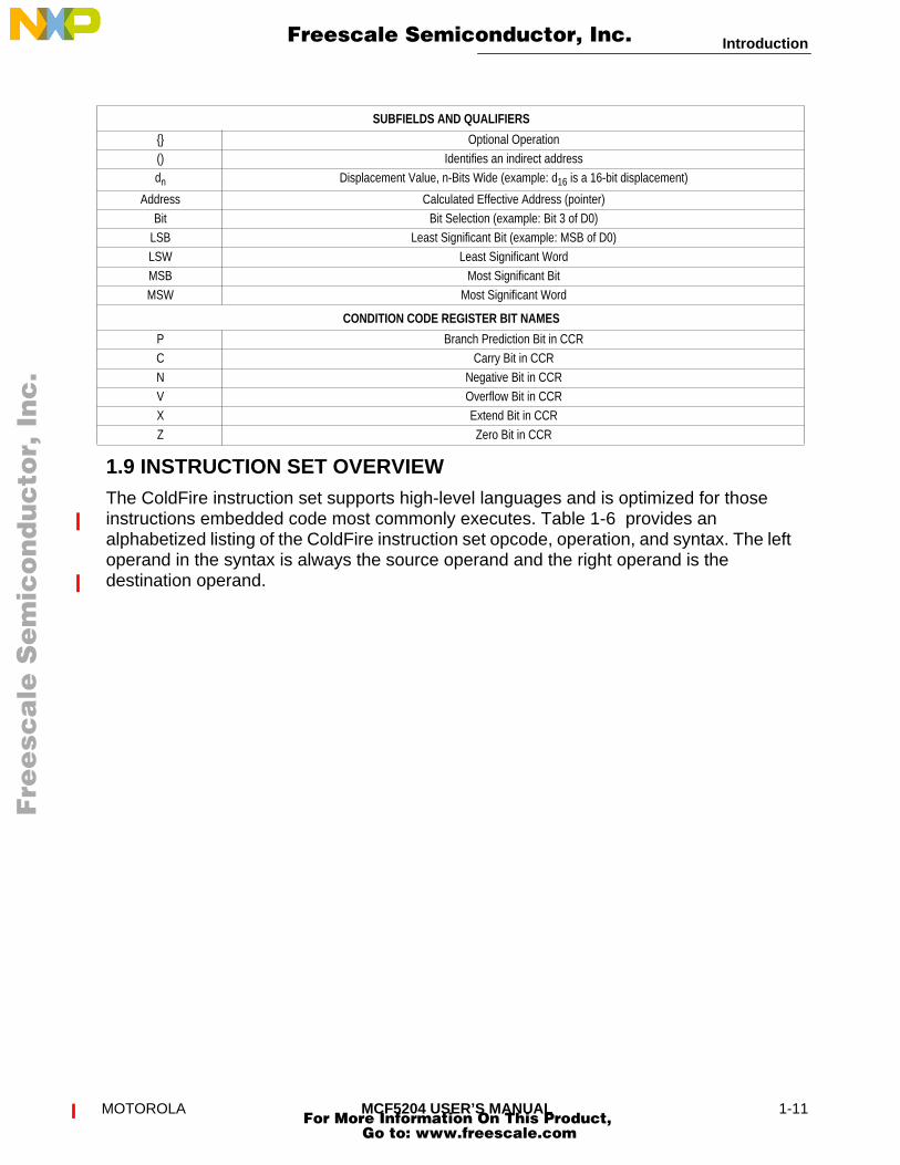
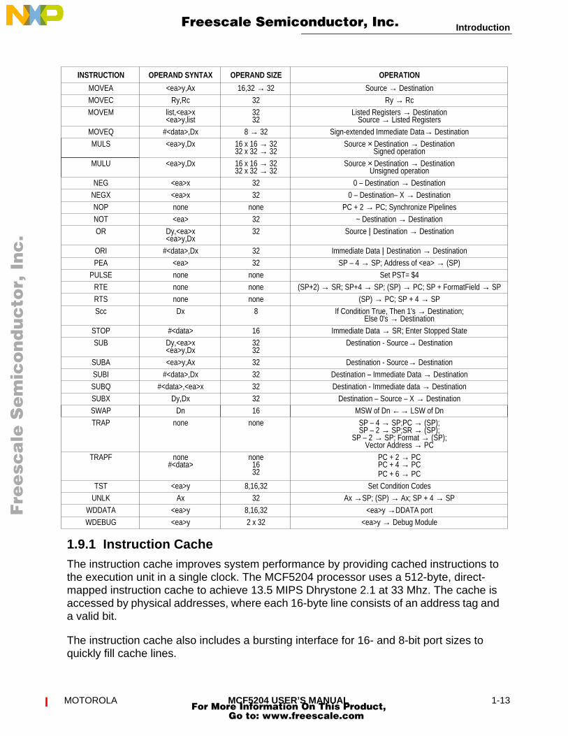
1.9 INSTRUCTION SET OVERVIEWThe ColdFire instruction set supports high-level languages and is optimized for those instructions embedded code most commonly executes. Table 1-6 provides an alphabetized listing of the ColdFire instruction set opcode, operation, and syntax. The left operand in the syntax is always the source operand and the right operand is the destination operand.
SUBFIELDS AND QUALIFIERS
{} Optional Operation() Identifies an indirect addressdn Displacement Value, n-Bits Wide (example: d16 is a 16-bit displacement)
Address Calculated Effective Address (pointer)Bit Bit Selection (example: Bit 3 of D0)
LSB Least Significant Bit (example: MSB of D0)LSW Least Significant WordMSB Most Significant BitMSW Most Significant Word
CONDITION CODE REGISTER BIT NAMES
P Branch Prediction Bit in CCRC Carry Bit in CCRN Negative Bit in CCRV Overflow Bit in CCRX Extend Bit in CCRZ Zero Bit in CCR
MOTOROLA MCF5204 USER’S MANUAL 1-11 For More Information On This Product,
Go to: www.freescale.com

Introduction
F
ree
sca
le S
em
ico
nd
uc
tor,
I
Freescale Semiconductor, Inc.n
c..
.
Table 1-6. Instruction Set Summary
INSTRUCTION OPERAND SYNTAX OPERAND SIZE OPERATION
ADD Dy,<ea>x<ea>y,Dx
3232
Source + Destination → Destination
ADDA <ea>y,Ax 32 Source + Destination → DestinationADDI #<data>,Dx 32 Immediate Data + Destination → DestinationADDQ #<data>,<ea>x 32 Immediate Data + Destination → DestinationADDX Dy,Dx 32 Source + Destination + X → DestinationAND Dy,<ea>x
<ea>y,Dx3232
Source & Destination → Destination
ANDI #<data>,Dx 32 Immediate Data & Destination → DestinationASL Dx,Dy
#<data>,Dx3232
X/C ← (Dy << Dx) ← 0X/C ← (Dy << #<data>) ← 0
ASR Dx,Dy<data>,Dx
3232
MSB → (Dy >> Dx) → X/CMSB → (Dy >> #<data>) → X/C
Bcc <label> 8,16 If Condition True, Then PC + dn → PC
BCHG Dy,<ea>x#<data>,<ea>x
8,328,32
~(<Bit Number> of Destination) → Z, Bit of Destination
BCLR Dy,<ea>x#<data>,<ea>x
8,328,32
~(<Bit Number> of Destination) → Z; 0 → Bit of Destination
BRA <label> 8,16 PC + dn → PC
BSET Dy,<ea>x#<data>,<ea>x
8,328,32
~(<Bit Number> of Destination) → Z; 1→ Bit of Destination
BSR <label> 8,16 SP – 4 → SP; next sequential PC→ (SP); PC + dn → PC
BTST Dy,<ea>x#<data>,<ea>x
8,328,32
~(<Bit Number> of Destination) → Z
CLR <ea>x 8,16,32 0 → DestinationCMPI #<data>,Dx 32 Destination – Immediate DataCMP <ea>y,Dx 32 Destination – Source
CMPA <ea>y,Ax 32 Destination - SourceCPUSH (An) 32 Push and Invalidate Cache Line
EOR Dy,<ea>x 32 Source ~ Destination → DestinationEORI #<data>,Dx 32 Immediate Data ~ Destination → DestinationEXT Dx
Dx8 → 16
16 → 32Sign-Extended Destination → Destination
EXTB Dx 8 → 32 Sign-Extended Destination → DestinationHALT none none Enter Halted StateJMP <ea> none Address of <ea> → PCJSR <ea> 32 SP– 4 → SP; next sequential PC → (SP); <ea> → PCLEA <ea>y,Ax 32 <ea> → AxLINK Ax,#<data> 16 SP – 4 → SP; Ax → (SP); SP → Ax; SP + d16 → SPLSL Dx,Dy
#<data>,Dx3232
X/C ← (Dy << Dx) ← 0X/C ← (Dx << #<data>) ← 0
LSR Dx,Dy#<data>,Dx
3232
0 → (Dy >> Dx) → X/C0 → (Dx >> #<data>) → X/C
MOVE <ea>y,<ea>x 8,16,32 <ea>y → <ea>xMOVE from CCR Dx 16 CCR → DxMOVE from SR Dx 16 SR → DxMOVE to CCR Dy,CCR
#<data>,CCR8 Dy → CCR
#<data> → CCRMOVE to SR Dy,SR
#<data>,SR16 Source → SR
1-12 MCF5204 USER’S MANUAL MOTOROLA For More Information On This Product,
Go to: www.freescale.com
Introduction
F
ree
sca
le S
em
ico
nd
uc
tor,
I
Freescale Semiconductor, Inc.n
c..
.
1.9.1 Instruction CacheThe instruction cache improves system performance by providing cached instructions to the execution unit in a single clock. The MCF5204 processor uses a 512-byte, direct-mapped instruction cache to achieve 13.5 MIPS Dhrystone 2.1 at 33 Mhz. The cache isaccessed by physical addresses, where each 16-byte line consists of an address tag and a valid bit.
The instruction cache also includes a bursting interface for 16- and 8-bit port sizes to quickly fill cache lines.
MOVEA <ea>y,Ax 16,32 → 32 Source → DestinationMOVEC Ry,Rc 32 Ry → RcMOVEM list,<ea>x
<ea>y,list3232
Listed Registers → DestinationSource → Listed Registers
MOVEQ #<data>,Dx 8 → 32 Sign-extended Immediate Data→ DestinationMULS <ea>y,Dx 16 x 16 → 32
32 x 32 → 32Source × Destination → Destination
Signed operationMULU <ea>y,Dx 16 x 16 → 32
32 x 32 → 32Source × Destination → Destination
Unsigned operationNEG <ea>x 32 0 – Destination → Destination
NEGX <ea>x 32 0 – Destination– X → DestinationNOP none none PC + 2 → PC; Synchronize PipelinesNOT <ea> 32 ~ Destination → DestinationOR Dy,<ea>x
<ea>y,Dx32 Source | Destination → Destination
ORI #<data>,Dx 32 Immediate Data | Destination → DestinationPEA <ea> 32 SP – 4 → SP; Address of <ea> → (SP)
PULSE none none Set PST= $4RTE none none (SP+2) → SR; SP+4 → SP; (SP) → PC; SP + FormatField → SPRTS none none (SP) → PC; SP + 4 → SPScc Dx 8 If Condition True, Then 1's → Destination;
Else 0's → DestinationSTOP #<data> 16 Immediate Data → SR; Enter Stopped StateSUB Dy,<ea>x
<ea>y,Dx3232
Destination - Source→ Destination
SUBA <ea>y,Ax 32 Destination - Source→ DestinationSUBI #<data>,Dx 32 Destination – Immediate Data → DestinationSUBQ #<data>,<ea>x 32 Destination - Immediate data → DestinationSUBX Dy,Dx 32 Destination – Source – X → DestinationSWAP Dn 16 MSW of Dn ←→ LSW of DnTRAP none none SP – 4 → SP;PC → (SP);
SP – 2 → SP;SR → (SP);SP – 2 → SP; Format → (SP);
Vector Address → PCTRAPF none
#<data>none
1632
PC + 2 → PCPC + 4 → PCPC + 6 → PC
TST <ea>y 8,16,32 Set Condition CodesUNLK Ax 32 Ax →SP; (SP) → Ax; SP + 4 → SP
WDDATA <ea>y 8,16,32 <ea>y →DDATA portWDEBUG <ea>y 2 x 32 <ea>y → Debug Module
INSTRUCTION OPERAND SYNTAX OPERAND SIZE OPERATION
MOTOROLA MCF5204 USER’S MANUAL 1-13 For More Information On This Product,
Go to: www.freescale.com
Introduction
Fre
esc
ale
Se
mic
on
du
cto
r, I
Freescale Semiconductor, Inc.n
c..
.
1.9.2 Internal SRAMThe 512-byte on-chip SRAM provides one clock-cycle access for the ColdFire core. This SRAM can store processor stack and critical code or data segments to maximize performance.
1.9.3 UART ModuleData formats can be 5, 6, 7, or 8 bits with even, odd, or no parity, and as many as two stop bits in 1/16 increments. Four-byte receive buffers and two-byte transmit buffers minimize CPU service calls. The UART module also provides several error-detection and maskable-interrupt capabilities. Modem support includes request-to-send (RTS) and clear-to-send (CTS) lines.
The system or external clock provides the clocking function via a programmable prescaler. Customers can select full duplex, autoecho loopback, local loopback, and remote loopback modes. The programmable UART can interrupt the CPU on various normal or error-condition events. UART pins can serve as general-purpose I/O, if needed.
1.9.4 Timers The MCF5204 includes two general-purpose timers, each of which contains a free-running 16-bit timer. One timer includes external package pins for use in any of three modes. Capture mode captures the timer value with an external event. “Trigger” mode triggers an external signal, while the “count” mode counts external events. Both timers can interrupt the CPU when the timer reaches a set value. Each timer has an 8-bit prescaler that allows programming of the clock input frequency, which is derived from the system clock. The programmable timer-output pin generates either an active-low pulse or toggles the output.
1.9.5 System Interface Module (SIM)The MCF5204 processor provides a glueless interface to 8- and 16-bit port size SRAM, ROM, FLASH and peripheral devices with independent programmable control of the assertion and negation of chip-selects and byte enables. In addition, the SIM contains an interrupt controller, general-purpose I/O, chip-selects, and other peripherals usually included in this module.
1.9.5.1 EXTERNAL BUS INTERFACE. The bus interface controller transfers information between the ColdFire core and memory and peripherals. The external bus interface provides as many as 22 bits of address bus space, a 16-bit data bus, and all associated control signals. This interface implements either a glueless asynchronous protocol that supports bursting operations or a synchronous protocol by adding external logic.
There are 22 physical address pins but 32 logical address internal signals.
1.9.5.2 CHIP-SELECTS. Six programmable chip-select outputs provide signals that enable external memory and peripheral circuits. These signals also interface to 8- and16-
1-14 MCF5204 USER’S MANUAL MOTOROLA For More Information On This Product,
Go to: www.freescale.com

Introduction
Fre
esc
ale
Se
mic
on
du
cto
r, I
Freescale Semiconductor, Inc.n
c..
.
bit ports. The base address, access permissions, wait-state insertion, write protection and automatic termination are all programmable with configuration registers.
1.9.5.3 8-BIT GENERAL PURPOSE I/O INTERFACE. An 8-bit general-purpose programmable I/O port serves as either an input or an output on a bit-by-bit basis. The parallel port is multiplexed with the timer, UART, and two of the upper address pins.
1.9.5.4 INTERRUPT CONTROLLER. The interrupt controller provides user-programmable control of four external interrupt and four internal peripheral interrupts. Customers can program any internal or external interrupt to any one of seven interrupt levels and four priority levels within each of these levels.
1.9.5.5 SYSTEM PROTECTION. The MCF5204 processor contains a 16-bit software watchdog timer with an 8-bit prescaler. The programmable software watchdog timer provides either a level 7 interrupt or a hardware reset on timeout. The MCF5204 processor also contains a reset status register that indicates the cause of the last reset.
1.9.5.6 JTAG. To help with system diagnostics and manufacturing testing, the MCF5204 processor includes dedicated user-accessible test logic that complies with the IEEE 1149.1 standard for boundary scan testability, often referred to as Joint Test Action Group, or JTAG. For more information, refer to the IEEE 1149.1 standard.
1.9.6 System Debug InterfaceThe ColdFire processor core debug interface supports real-time trace and Background-Debug mode. A four-pin Background-Debug mode (BDM) interface provides system debug. The BDM is a proper subset of the BDM interface provided on Motorola’s 683XX Family of parts.
In real-time trace, four status lines provide information on processor activity in real time (PST pins). A 4-bit wide debug data bus (DDATA) displays operand data, which helps track the machine’s dynamic execution path as the change-of-flow instructions execute.
1.9.7 Power ManagementThe MCF5204 is very power-efficient because of its small die size and static design. Power consumption can be controlled on the MCF5204 by lowering the frequency of operations when performance is less critical.
In addition, execution of the STOP instruction places the ColdFire core in a low-power state. Customers can resume processing by resetting the part or generating a trace or interrupt.
1.9.8 Pinout and PackageThe MCF5204 device is supplied in a 100-pin plastic thin quad flat pack package.
MOTOROLA MCF5204 USER’S MANUAL 1-15 For More Information On This Product,
Go to: www.freescale.com

DATE: 08-21-98
REVISION NO: 0.1
PAGES AFFECTED: SEE CHANGE BARS
F
ree
sca
le S
em
ico
nd
uc
tor,
I
Freescale Semiconductor, Inc.n
c..
.
SECTION 2SIGNAL DESCRIPTIONS
2.1 SIGNALS OVERVIEW
Figure 2-1. MCF5204 Pinout Block Diagram
A[19:0]
D[15:0]
REWE
UWELWE
DTACKBUSW/ATS
CS[5:0]
IRQ[3:0]
CLKRESET
TIN/PP2TOUT/PP3
RXD/PP5TXD/PP4RTS/PP7CTS/PP6
BKPT/TMS
DSI/TDIDSO/TDO
DSCLK/TRSTTCLK
MTMOD
A[20]/PP0A[21]/PP1
DDATA[3:0]
PST[3:0] (HIZ)4
4
4
6
16
22
32
32
COLDFIRECORE
512 BYTESRAM
512 BYTECACHE
DEBUGMODULE
JTAGPORT
CLOCK
INTERRUPTCONTROLLER
CHIPSELECTS
SYSTEMBUSCONTROLLER
BUSINTERFACE
TIMER 2
TIMER 1
UART
PARALLELPORT
MOTOROLA MCF5204 USER’S MANUAL 2-1 For More Information On This Product,
Go to: www.freescale.com

Signal Description
F
ree
sca
le S
em
ico
nd
uc
tor,
I
Freescale Semiconductor, Inc.n
c..
.
The signal index that follows provides a detailed description of the pin characteristics.
2.1.1 Signal Index Field DefinitionsWhat follows is a brief description of the headings used in the signal index table:
Signal Name: Indicates the name of this signal, which is the name used throughoutthis manual.
Alt. Function: Alternate function, if any, that is multiplexed onto this pin. Controlregisters activate these alternate functions under program control.
Reset Function: Alternate function of this pin is determined at reset negation. Thisalternate function is activated by sampling the values on a pin at thetime of RESET negation. The -ctl suffix indicates the pin that is usedto control this reset configuration.
Pin Count: The number of physical pins associated with this function.
Pin Type: Type of pin, Input(I), Output(O) or Bidirectional(I/O).
This field also indicates if there is no JTAG cell associated with this pin, NJ -> No JTAG cell associated with this pin
Buffer Sizes: Indicates the size of the output buffer associated with this pin. All out-put buffers are 8mA except for all address data, UWE, LWE, RE, WEsignals.
Reset State: The driven state of this pin while RESET is asserted1 - Output is driven to logic one during RESET assertion
‘ 0 - Output is driven to logic zero during RESET assertionz - Output is three-stated during RESET assertion
Assertion Edge: Indicates the clock edge on which transitions of this signal occurSync: Indicates if a synchronizer cell synchronizes this signal internally
Debug: Defines the functionality of these pins during debug (i.e. MTMOD asserted)
2-2 MCF5204 USER’S MANUAL MOTOROLA For More Information On This Product,
Go to: www.freescale.com
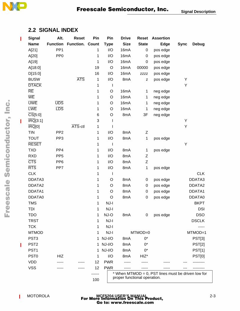
Signal Description
F
ree
sca
le S
em
ico
nd
uc
tor,
I
Freescale Semiconductor, Inc.n
c..
.
2.2 SIGNAL INDEXSignal Alt. Reset Pin Pin Drive Reset Assertion
Name Function Function. Count Type Size State Edge Sync Debug
A[21] PP1 1 I/O 16mA 0 pos edge
A[20] PP0 1 I/O 16mA 0 pos edge
A[19] 1 I/O 16mA 0 pos edge
A[18:0] 19 O 16mA 00000 pos edge
D[15:0] 16 I/O 16mA zzzz pos edge
BUSW ATS 1 I/O 8mA z pos edge Y
DTACK 1 I Y
RE 1 O 16mA 1 neg edge
WE 1 O 16mA 1 neg edge
UWE UDS 1 O 16mA 1 neg edge
LWE LDS 1 O 16mA 1 neg edge
CS[5:0] 6 O 8mA 3F neg edge
IRQ[3:1] 3 I Y
IRQ[0] ATS-ctl 1 I Y
TIN PP2 1 I/O 8mA Z
TOUT PP3 1 I/O 8mA 1 pos edge
RESET 1 I Y
TXD PP4 1 I/O 8mA 1 pos edge
RXD PP5 1 I/O 8mA Z
CTS PP6 1 I/O 8mA Z
RTS PP7 1 I/O 8mA 1 pos edge
CLK 1 I CLK
DDATA3 1 O 8mA 0 pos edge DDATA3
DDATA2 1 O 8mA 0 pos edge DDATA2
DDATA1 1 O 8mA 0 pos edge DDATA1
DDATA0 1 O 8mA 0 pos edge DDATA0
TMS 1 NJ-I BKPT
TDI 1 NJ-I DSI
TDO 1 NJ-O 8mA 0 pos edge DSO
TRST 1 NJ-I DSCLK
TCK 1 NJ-I -----
MTMOD 1 NJ-I MTMOD=0 MTMOD=1
PST3 1 NJ-I/O 8mA 0* PST[3]
PST2 1 NJ-I/O 8mA 0* PST[2]
PST1 1 NJ-I/O 8mA 0* PST[1]
PST0 HIZ 1 I/O 8mA HIZ* PST[0]
VDD ----- ----- 12 PWR ----- ----- ----- --- ---------
VSS ----- ----- 12 PWR ----- ----- ----- --- ---------
------
100
* When MTMOD = 0, PST lines must be driven low for proper functional operation.
MOTOROLA MCF5204 USER’S MANUAL 2-3 For More Information On This Product,
Go to: www.freescale.com

Signal Description
F
ree
sca
le S
em
ico
nd
uc
tor,
I
Freescale Semiconductor, Inc.n
c..
.
2.3 SIGNAL DEFINITIONSIn the following sections, the primary signal name is listed first followed in parenthesis by alternate or multiplexed functions.
2.3.1 External Bus Signals2.3.1.1 ADDRESS BUS A[21:20]/(PP[1:0]). Address bus signals A[21:20] are multi-
plexed with parallel port bits.When programmed as general-purpose input/output, eachpin functions as bit 1 and 0 of the general-purpose I/O.
2.3.1.2 ADDRESS BUS—(A[19:0]). The address bus signals are outputs that define theaddress of the byte (or most significant byte) to be transferred during a bus cycle. TheMCF5240 places the address on the bus at the beginning of a bus cycle. The addressis valid while CS is asserted. During an interrupt acknowledge access, the lower ad-dress lines, A[4:2], indicate the interrupt level being acknowledged.
2.3.1.3 DATA BUS—(D[15:0]). This bidirectional, nonmultiplexed, parallel bus containsthe data being transferred to or from the MCF5204. Data is latched on the bus on therising clock edge. A read or write operation may transfer 8 or 16 bits of data (one or twobytes) in one bus cycle. For a write cycle, all 16 bits of the data bus are driven, regard-less of the port width or operand size. BUSW, which is sampled at reset, determinesthe boot data bus port width.
During reset, BUSW initially defines the data bus port width. After global chip-select is negated, the configuration register programs the port width for each chip-select(see Table 2-1). The data bus transfers byte or word-sized data.
2.3.2 BUS CONTROL2.3.2.1 Data Transfer Acknowledge DTACK. This active-low input signal allows asyn-
chronous termination of external accesses between the MCF5204 and external devic-es. During bus cycles, external devices assert DTACK as part of the bus protocol.During a read cycle this signal determines that the MCF5204 has terminated the buscycle to latched data. Data is latched one clock after the assertion of DTACK. During awrite cycle, this signal indicates that the external device has successfully stored thedata and that the cycle can terminate.
2.3.2.2 Read Enable—(R E). This active-low output indicates that the MCF5204 is readyto read the data. The external peripheral or memory should enable the data out whileRE is asserted.
Table 2-1. Chip-Select Port Width
BUSW AT RESET PORT WIDTH0 16 Bit1 8 Bit
2-4 MCF5204 USER’S MANUAL MOTOROLA For More Information On This Product,
Go to: www.freescale.com

Signal Description
F
ree
sca
le S
em
ico
nd
uc
tor,
I
Freescale Semiconductor, Inc.n
c..
.
2.3.2.3 Write Enable—(W E). This active-low output signal indicates the direction of adata transfer on the data bus. A logic one indicates a read from a slave device; a logiczero indicates a write to a slave device.
2.3.2.4 Upper Write Enable—(UWE /UDS) and Lower Write Enable—(LWE /LDS). Ona write to a 16-bit port, the UWE/LWE active-low output signals indicate when the upperor lower eight bits of the data bus contain valid data. The upper write enable indicatesthat the upper eight bits of the data bus contain valid data during a write cycle.The lowerwrite enable indicates that the lower eight bits of the data bus contain valid data duringa write cycle. UWE and LWE do not assert on a read cycle.
See Table 2-2 for reference.
In an alternate mode controlled by chip-select configuration, these pins can be definedto operate as Upper Data Strobe/Lower Data Strobe UDS/LDS. These active-low sig-nals control the data flow on the MCF5204 data bus. UDS and LDS are asserted onboth reads and writes.
See Table 2-3 for reference.
In 8-bit-wide bus port size (programmed in conjunction with chip-selects), all bus cyclesappear as 8-bit reads or writes to the upper half of the data bus (D[15:8]), and so onlyUDS is asserted. You should use A0 to determine if the even or odd byte is being ad-dressed; it is valid whenever the external CS signal is asserted during such a cycle.
Table 2-2. Write Enable Control of Data Bus
UWE LWE WE D15 - D8 D7 - D01 1 1 HIZ HIZ0 0 0 Valid Data Valid Data0 1 0 Valid Data No Value1 0 0 No Value Valid Data1 1 0 No Value No Value
Table 2-3. Data Strobe Control of Data Bus
UDS LDS WE D[15:8] D[7:0]
High High - No Valid Data No Valid Data
Low Low High Valid Data Valid Data
High Low High No Valid Data Valid Data
Low High High Valid Data No Valid Data
Low Low Low Valid Data Valid Data
High Low Low No Valid Data Valid Data
Low High Low Valid Data No Valid Data
MOTOROLA MCF5204 USER’S MANUAL 2-5 For More Information On This Product,
Go to: www.freescale.com

Signal Description
F
ree
sca
le S
em
ico
nd
uc
tor,
I
Freescale Semiconductor, Inc.n
c..
.
There is no external indication of data bus width other than the chip-select asserted. You have the knowledge of which bus width that chip-select is programmed to providefor any given configuration of the MCF5204 in a system.
2.3.2.5 BUS WIDTH—(BUSW/ATS ).
BUSWThe BUSW input signal indicates the port size of the external boot device. The state onthis input pin is read at reset and is used to select the data bus width for memory accessfor CS0 during global chip-select. Hold BUSW high for an 8-bit data bus, or low for a16- bit data bus during bus cycles that trigger CS0 during global chip-select. BUSWdoes not choose the bus width for CS[1:5]. That is done by user initialization code. TheBUSW input value is used only for global CS0; programming the CS0 control registerdetermines the bus width for CS0 after global chip-select.
ATSATS, Address Transition Start, is an active-low signal that indicates an address transi-tion has occurred and that a decode of the address can start at the next rising clockedge. This signal can be used with programmable logic that latches inputs on risingedge of CLK. The ATS signal provides an early indication to external logic that an ex-ternal address is valid at the subsequent clock edge and a bus cycle has started. Thisearly indication saves a CLK since logic does not have to wait until the assertion of chip-selects and bus strobes. Asserting IRQ0 at reset enables ATS.
2.3.3 EXCEPTION CONTROL SIGNALS2.3.3.1 Reset (RESET). This active-low signal initiates a system reset. The assertion
of RESET will cause the MCF5204 processor to enter reset exception processing. Atreset, all bus control signal and chip-selects are driven inactive, the address bus is driv-en to all zeros, and the data bus is three-stated.
2.3.4 CHIP-SELECT SIGNALSThe MCF5204 provides six programmable chip-selects that can directly interface with SRAM, EPROM, EEPROM, and peripherals.
2.3.4.1 Chip-Selects (C S[5:0]). The chip-select output signals enable peripherals atprogrammed addresses. Each chip-select can be programmed for an address locationas well as for masking capabilities, port size, bursting, wait-state generation, internal/external termination, and byte enables. A reset disables these chip-selects.
These signals are inactive-high after reset. CS0 is the global chip-select for a boot ROMcontaining the program counter, stack pointer, and initialization program. It functions asthe global chip-select immediately after reset. You can program any chip-select to pro-vide an interrupt acknowledge indication. Out of reset, the global chip-select operateswith maximum wait states (7). BUSW determines port width.
2-6 MCF5204 USER’S MANUAL MOTOROLA For More Information On This Product,
Go to: www.freescale.com

Signal Description
F
ree
sca
le S
em
ico
nd
uc
tor,
I
Freescale Semiconductor, Inc.n
c..
.
2.3.5 INTERRUPT REQUEST SIGNALS—(IRQ[3:0])Interrupt request lines are the external interrupt inputs to the ColdFire core. These pins have their associated interrupt priority level set by programming internal registers. IRQ[0] is sampled at reset to determine the function of the BUSW/ATS pin.
2.3.6 CLOCK SIGNALS—(CLK)CLK is the MCF5204 processor synchronous clock and internally clocks or sequences the MCF5204 processor internal logic.
2.3.7 TIMER SIGNALS2.3.7.1 TIMER INPUT—(TIN/PP2). You can program this bidirectional signal as a clock
input that causes events to occur in the timer/counter, either causing a clock to theevent counter or providing a trigger to the timer value capture logic.
TIN is also connected as the external clock for the serial module. No action is requiredto activate this feature, but you should use caution with software to ensure that UARTexternal clock mode is activated exclusively of TIN being used as a timer input.
When programmed as general-purpose I/O, this pin functions as bit 2 of the general-purpose I/O.
2.3.7.2 TIMER OUTPUT—(TOUT/PP3). You can program this bidirectional signal to tog-gle or pulse for one system clock duration when the timer/counter reaches a referencevalue.
When programmed as a general-purpose I/O, this pin functions as bit 3 of the general-purpose I/O.
2.3.8 SERIAL SIGNALS2.3.8.1 TRANSMIT DATA —(TXD/PP4) . This signal is the transmitter serial data output
for the serial module. The output is held high (“mark” condition) when the transmitter isdisabled, idle, or operating in the local loopback mode. Data is shifted out on this signalwith the least significant bit transmitted first.
When programmed as general-purpose I/O, this pin functions as bit 4 of the general-purpose I/O.
2.3.8.2 RECEIVE DATA—(RXD/PP5). This signal is the receiver serial data input to theserial module. Data received on this signal is sampled with the least significant bit re-ceived first.
When programmed as general-purpose I/O, this pin functions as bit 5 of the general-purpose I/O.
MOTOROLA MCF5204 USER’S MANUAL 2-7 For More Information On This Product,
Go to: www.freescale.com

Signal Description
F
ree
sca
le S
em
ico
nd
uc
tor,
I
Freescale Semiconductor, Inc.n
c..
.
2.3.8.3 CLEAR TO SEND —(CTS/PP6). This active-low signal is the Clear-To-Send in-put for the serial module. Peripherals drive this input to indicate to the MCF5204 serialmodule that it can begin data transmission.
When programmed as general-purpose I/O, this pin functions as bit 6 of the general-purpose I/O.
2.3.8.4 REQUEST TO SEND—(RTS/PP7). This active-low signal is the Request-To-Send output for the serial module. It indicates to the peripheral device that the UART isready to send data and requires a Clear-To-Send signal to initiate transfer.
When programmed as general-purpose I/O, this pin functions as bit 7 of the general-purpose I/O.
2.3.9 Test and Debug Signals2.3.9.1 MTMOD. This signal chooses between the BDM/RTT and JTAG signals that are
multiplexed together. When MTMOD=1, the part is in BDM mode; MTMOD=0 is JTAG/functional mode. MTMOD should not be changed while RESET = 1.
2.3.9.2 BREAK POINT—(B KPT/TMS). The MTMOD signals determine this pin’s dualfunction. If MTMOD = 0, then the TMS function is selected. If MTMOD =1, the BKPTfunction is selected. MTMOD should not change while RESET = 1.
BKPTBKPT is an active-low signal that signals a hardware breakpoint for the ColdFire core.When in the debug mode, BKPT signals a hardware breakpoint to the processor. SeeSection 10: Debug Support for additional information on this signal.
TMSTMS controls test mode operations for the onboard test logic defined by IEEE 1149.1standard.
When used as TMS, this input signal provides the JTAG controller with information todetermine which test operation mode should be performed. The value of TMS and cur-rent state of the internal 16-state JTAG controller state machine at the rising edge ofTCK determines whether the JTAG controller holds its current state or advances to thenext state. This directly controls whether JTAG data or instruction operations occur.TMS has an internal pullup so that if it is not driven low, its value will default to a logiclevel of 1. However, if TMS will not be used, it should be tied to VDD. See Section 11 :JTAG Support for additional information on this signal.
2.3.9.3 DEBUG SERIAL DATA INPUT—(DSI/TDI). This is a dual-function pin. If MTMOD = 0, then TDI is selected. If MTMOD = 1, then DSI is selected.
2-8 MCF5204 USER’S MANUAL MOTOROLA For More Information On This Product,
Go to: www.freescale.com

Signal Description
F
ree
sca
le S
em
ico
nd
uc
tor,
I
Freescale Semiconductor, Inc.n
c..
.
DSIThis development serial input helps provide serial communications for the backgrounddebug mode. DSI also provides the single-bit communication for the debug modulecommands. See Section 10: Debug Support for additional information on this signal.
TDIThis input is used for serial test instructions and data for the onboard test logic definedby the IEEE 1149.1 standard.
When used as TDI, this input signal provides the serial data port for loading the variousJTAG shift registers such as the boundary scan, the bypass, and the instruction regis-ters. Shifting in of data depends on the state of the JTAG controller state machine andthe instruction currently in the instruction register. This data shift occurs on the risingedge of TCK. TDI also has an internal pullup so that if it is not driven low its value willdefault to a logic level of 1. However, if TDI will not be used, it should be tied to VDD.See Section 11: JTAG Support for more information.
2.3.9.4 DEBUG SERIAL DATA OUTPUT—(DSO/TDO). This is a dual-function pin.When MTMOD = 0, TDO is selected. When MTMOD = 1, then DSO is selected.
DSOThis development serial output helps provide serial communications for the back-ground-debug mode. DSO provides single-bit communication for the Debug module re-sponses. See Section 10: Debug Support for additional information on this signal.
TDOThis output is used for serial test instructions and data for the onboard test logic definedby IEEE 1149.1 standard.
When used as TDO, this output signal provides the serial data port for outputting datafrom the JTAG logic. The shifting out of data depends on the state of the JTAG control-ler state machine and the instruction currently residing in the instruction register. Thisdata shift occurs on the falling edge of TCK. When TDO is not outputting test data, it isplaced in a three-state mode. TDO can also be placed in three-state mode to allowbussed or parallel connections to other devices having JTAG. See Section 11: JTAGSupport for more information.
2.3.9.5 DEBUG SERIAL CLOCK—DSCLK (TRST ) . The MTMOD signal determinesthe function of this dual-purpose pin. If MTMOD = 0, the TRST function is selected. IfMTMOD =1, the DSCLK function is selected.
DSCLKThis development serial clock helps provide serial communications for serial interfaceto the Debug module. The maximum frequency for the DSCLK signal is one-half theCLK frequency. See Section 10: Debug Support for additional information on this signal.
MOTOROLA MCF5204 USER’S MANUAL 2-9 For More Information On This Product,
Go to: www.freescale.com

Signal Description
F
ree
sca
le S
em
ico
nd
uc
tor,
I
Freescale Semiconductor, Inc.n
c..
.
TRST This input is used by the onboard test logic defined by the IEEE 1149.1 standard.
When used as TRST, this pin will asynchronously reset the internal JTAG controller tothe test logic reset state, causing the JTAG instruction register to choose the “bypass”command. When this occurs, all the JTAG logic is benign and will not interfere with thenormal functionality of the MCF5204 processor. Although this is an asynchronous sig-nal, Motorola recommends that TRST make only a 0 to 1 (asserted to negated) transi-tion while TMS is held at a logic 1 value. TRST has an internal pullup so that if it is notdriven low its value will default to a logic level of 1. However, if TRST will not be used,it can either be tied to ground or, if TCK is clocked, it can be tied to VDD. The formerconnection will place the JTAG controller in the test logic reset state immediately whilethe later connection will cause the JTAG controller (if TMS is a logic 1) to eventually re-side in the test logic reset state after 5 clocks of TCK.
2.3.9.6 JTAG CLOCK—(TCLK). This input provides a clock for the onboard test logicdefined by the IEEE 1149.1 standard.
TCK is the dedicated JTAG test logic clock that is independent of the MCF5204 proces-sor clock. Various JTAG operations occur on the rising or falling edge of TCK. The in-ternal JTAG controller logic is designed such that holding TCK high or low for anindefinite period of time will not cause the JTAG test logic to lose state information. IfTCK will not be used, it should be tied to ground.
2.3.9.7 DEBUG DATA —(DDATA[3:0]). This nibble-wide bus displays captured proces-sor data and breakpoint status. See Section 10: Debug Support for additional infor-mation on this bus.
2.3.9.8 PROCESSOR STATUS—(PST/HIZ[3:0]).
PST[3:0]These outputs indicate the MCF5204 processor status. During debug mode, the timingis synchronous with the processor clock (CLK) and the status is not related to the cur-rent bus transfer. Table 2-4 shows the encoding of these signals. When MTMOD
2-10 MCF5204 USER’S MANUAL MOTOROLA For More Information On This Product,
Go to: www.freescale.com

Signal Description
F
ree
sca
le S
em
ico
nd
uc
tor,
I
Freescale Semiconductor, Inc.n
c..
.
= 1, PST pins are active; when MTMOD = 0, PST pins and the HIZ pin are three-stated.
HIZThis input causes all outputs to go to a high-impedance state and is used only for testpurposes. The assertion of HIZ will force all output drivers to a high-impedance state.The timing on HIZ is independent of the clock. Note that HIZ does not override the JTAGoperation; TDO/DSO can be forced to high impedance by asserting TRST.
HIZ is only active while MTMOD=0 and is multiplexed with PST[0].
Table 2-4. PST Signal Encoding
PST[3:0] DEFINITION
0000 Continue execution
0001 Begin execution of an instruction
0010 Reserved
0011 Entry into user-mode
0100 Begin execution of PULSE instruction
0101 Begin execution of taken branch
0110 Reserved
0111 Begin execution of RTE instruction
1000 Reserved
1001 Reserved
1010 Reserved
1011 Reserved
1100 † Exception processing
1101 † Emulator-mode entry exception processing
1110 † Processor is stopped, waiting for interrupt
1111 † Processor is halted
† These encodings are asserted for multiple cycles.
MOTOROLA MCF5204 USER’S MANUAL 2-11 For More Information On This Product,
Go to: www.freescale.com

DATE: 08-21-98
REVISION NO: 0.1
PAGES AFFECTED: SEE CHANGE BARS
F
ree
sca
le S
em
ico
nd
uc
tor,
I
Freescale Semiconductor, Inc.n
c..
.
SECTION 3COLDFIRE CORE
This section describes the organization of the ColdFire 5200 processor core and an overview of the program-visible registers. For detailed information on instructions, see the ColdFire Microprocessor Family Programmer’s Reference Manual.
3.1 PROCESSOR PIPELINESFigure 3-1 is a block diagram showing the processor pipelines of a ColdFire 5200 core.
Figure 3-1. ColdFire 5200 Processor Core Pipelines
IA GENERATION
INSTRUCTIONFETCH
FIFOINSTRUCTION
BUFFER
DECODE & SELECT,OPERAND FETCH
ADDRESSGENERATION,
EXECUTE
IFP
OEP
ADDRESS[31:0]
DATA[31:0]
MOTOROLA MCF5204 USER’S MANUAL 3-1 For More Information On This Product,
Go to: www.freescale.com

ColdFire Core
Fre
esc
ale
Se
mic
on
du
cto
r, I
Freescale Semiconductor, Inc.n
c..
.
The processor core is comprised of two separate pipelines that are decoupled by an instruction buffer. The Instruction Fetch Pipeline (IFP) is responsible for instruction address generation and instruction fetch. The instruction buffer is a first-in-first-out (FIFO) buffer that holds prefetched instructions awaiting execution in the Operand Execution Pipeline (OEP). The OEP includes two pipeline stages. The first stage decodes instructions and selects operands (DSOC); the second stage (AGEX) performs instruction execution and calculates operand effective addresses, if needed.
3.2 PROCESSOR REGISTER DESCRIPTIONThe following paragraphs describe the processor registers in the user and supervisor programming models. The appropriate programming model is selected based on the privilege level (user mode or supervisor mode) of the processor as defined by the S-bit of the status register.
3.2.1 User Programming ModelFigure 3-2 illustrates the user programming model. The model is the same as for M68000Family microprocessors, consisting of the following registers:
• 16 general-purpose 32-bit registers (D0–D7, A0–A7)
• 32-bit program counter (PC)
• 8-bit condition code register (CCR)
3.2.1.1 DATA REGISTERS (D0–D7). Registers D0–D7 are used as data registers for bit (1 bit), byte (8 bit), word (16 bit) and longword (32 bit) operations and can also be used as index registers.
3.2.1.2 ADDRESS REGISTERS (A0–A6). These registers can be used as software stack pointers, index registers, or base address registers as well as for word and longword operations.
3.2.1.3 STACK POINTER (A7). ColdFire supports a single hardware stack pointer (A7) for explicit references or implicit ones during stacking for subroutine calls and returns and exception handling. The initial value of A7 is loaded from the reset exception vector, address $0. The same register is used for both user and supervisor mode as well as word and longword operations.
A subroutine call saves the PC on the stack and the return restores it from the stack. Both the PC and the SR are saved on the stack during the processing of exceptions and interrupts. The return from exception instruction restores the SR and PC values from the stack.
3.2.1.4 PROGRAM COUNTER. The PC contains the address of the currently executing instruction. During instruction execution and exception processing, the processor automatically increments the contents of the PC or places a new value in the PC, as appropriate. For some addressing modes, the PC can be used as a pointer for PC-relative operand addressing.
3-2 MCF5204 USER’S MANUAL MOTOROLA For More Information On This Product,
Go to: www.freescale.com

ColdFire Core
F
ree
sca
le S
em
ico
nd
uc
tor,
I
Freescale Semiconductor, Inc.n
c..
.
3.2.1.5 CONDITION CODE REGISTER . The CCR is the least significant byte of the processor status register (SR), as shown in Figure 3-3. Bits 4–0 represent indicator flags based on results generated by processor operations. Bit 4, the extend bit (X-bit), is also used as an input operand during multiprecision arithmetic computations.
Figure 3-2. User Programming Model
4 3 2 1 0X N Z V C
D0D1D2D3D4D5D6D7
A0A1A2A3A4A5A6
A7
CCR
PC
15 7 0
15 031
DATAREGISTERS
ADDRESSREGISTERS
STACKPOINTER
PROGRAMCOUNTER
CONDITIONCODEREGISTER
7
MOTOROLA MCF5204 USER’S MANUAL 3-3 For More Information On This Product,
Go to: www.freescale.com

ColdFire Core
F
ree
sca
le S
em
ico
nd
uc
tor,
I
Freescale Semiconductor, Inc.n
c..
.
X— extend condition code bit
N– negative condition code bitSet if the most significant bit of the result is set; otherwise cleared
Z– zero condition code bitSet if the result equals zero; otherwise cleared
V– overflow condition code bitSet if an arithmetic overflow occurs implying that the result cannot be represented in theoperand size; otherwise cleared
C– carry condition code bitSet if a carryout of the operand MSB occurs for an addition, or if a borrow occurs in asubtraction; otherwise cleared
Set to the value of the C-bit for arithmetic operations; otherwise not affected.
3.2.2 Supervisor Programming ModelOnly system programmers use the supervisor programming model (see Figure 3-3) to implement sensitive operating system functions, I/O control, and memory management. All accesses that affect the control features of ColdFire 5200 processors are in the supervisor programming model, which consists of the registers available to users as well as the following control registers:
• 16-bit status register (SR)
• 32-bit vector base register (VBR)
Figure 3-3. Supervisor Programming Model
Additional registers may be supported on a part basis.
The following paragraphs describe the supervisor programming model registers.
3.2.2.1 STATUS REGISTER. The SR (see Figure 3-4) stores the processor status and includes the CCR, the interrupt priority mask, and other control bits. In the supervisor mode, software can access the entire SR. In user mode, only the lower 8 bits are
31 20 19 0MUST BE ZEROS VBR VECTOR BASE REGISTER
15 8 7 0System Byte CCR SR STATUS REGISTER
3-4 MCF5204 USER’S MANUAL MOTOROLA For More Information On This Product,
Go to: www.freescale.com

ColdFire Core
F
ree
sca
le S
em
ico
nd
uc
tor,
I
Freescale Semiconductor, Inc.n
c..
.
accessible (CCR). The control bits indicate the following states for the processor: trace mode (T-bit), supervisor or user mode (S-bit), and master or interrupt state (M).
T– trace enableWhen set, the processor will perform a trace exception after every instruction.
S– supervisor / user stateDenotes whether the processor is in supervisor mode (S=1) or user mode (S=0).
M– master / interrupt stateThis bit is cleared by an interrupt exception, and can be set by software during execu-tion of the RTE or move to SR instructions.
I[2:0]– interrupt priority maskDefines the current interrupt priority. Interrupt requests are inhibited for all priority levelsless than or equal to the current priority, except the edge-sensitive level 7 request,which cannot be masked.
3.2.2.2 VECTOR BASE REGISTER (VBR). The VBR in the ColdFire architecture is a 32-bit address register with only the upper 12 bits physically implemented in hardware. The low-order 20 bits are forced to zero when the CPU uses the VBR to calculate the exception vector address, effectively placing the vector table on a 0-modulo-1 MByte address.
The VBR may be written using the MOVEC instruction from the CPU, or from a BDM serial command. The register may be read from BDM only. When a BDM read of the VBR is performed, the contents of the register are returned in the upper 12 bits of the 32-bit result, with the low-order 20 bits being UNDEFINED.
The ColdFire 5200 processors provide a simplified exception processing model. The next section details the model.
3.3 EXCEPTION PROCESSING OVERVIEWException processing for ColdFire processors is streamlined for performance. Differences from previous 68000 Family processors include:
• A simplified exception vector table
• Reduced relocation capabilities using the vector base register
• A single exception stack frame format
• Use of a single self-aligning system stack
SYSTEM BYTE CONDITION CODE REGISTER (CCR)15 14 13 12 11 10 9 8 7 6 5 4 3 2 1 0T 0 S M 0 I[2:0] 0 0 0 X N Z V C
Figure 3-4. Status Register
MOTOROLA MCF5204 USER’S MANUAL 3-5 For More Information On This Product,
Go to: www.freescale.com

ColdFire Core
F
ree
sca
le S
em
ico
nd
uc
tor,
I
Freescale Semiconductor, Inc.n
c..
.
ColdFire 5200 processors use an instruction restart exception model but do require more software support to recover from certain access errors. See subsection 3.5.1 Access Error Exception for details.
Exception processing is comprised of four major steps and can be defined as the time from the detection of the fault condition until the fetch of the first handler instruction has been initiated.
First, the processor makes an internal copy of the SR and then enters supervisor mode by asserting the S-bit and disabling trace mode by negating the T-bit. The occurrence of an interrupt exception also forces the M-bit to be cleared and the interrupt priority mask to be set to the level of the current interrupt request.
Second, the processor determines the exception vector number. For all faults except interrupts, the processor performs this calculation based on the exception type. For interrupts, the processor performs an interrupt-acknowledge (IACK) bus cycle to obtain the vector number from a peripheral device. The IACK cycle is mapped to a special acknowledge address space with the interrupt level encoded in the address.
Third, the processor saves the current context by creating an exception stack frame on the system stack. ColdFire 5200 processors support a single stack pointer in the A7 address register; therefore, there is no notion of separate supervisor or user stack pointers. As a result, the exception stack frame is created at a 0-modulo-4 address on the top of the current system stack. Additionally, the processor uses a simplified fixed-length stack frame for all exceptions. The exception type determines whether the program counter placed in the exception stack frame defines the location of the faulting instruction (fault) or the address of the next instruction to be executed (next).
Fourth, the processor calculates the address of the first instruction of the exception handler. By definition, the exception vector table is aligned on a 1 Mbyte boundary. This instruction address is generated by fetching an exception vector from the table located at the address defined in the vector base register. The index into the exception table is calculated as (4 x vector_number). Once the exception vector has been fetched, the contents of the vector determine the address of the first instruction of the desired handler. After the instruction fetch for the first opcode of the handler has been initiated, exception processing terminates and normal instruction processing continues in the handler.
ColdFire 5200 processors support a 1024-byte vector table aligned on any 1 Mbyte address boundary (see Table 3-1). The table contains 256 exception vectors where the first 64 are defined by Motorola and the remaining 192 are user-defined interrupt vectors.
3-6 MCF5204 USER’S MANUAL MOTOROLA For More Information On This Product,
Go to: www.freescale.com

ColdFire Core
F
ree
sca
le S
em
ico
nd
uc
tor,
I
Freescale Semiconductor, Inc.n
c..
.
ColdFire 5200 processors inhibit sampling for interrupts during the first instruction of all exception handlers. This allows any handler to effectively disable interrupts, if necessary, by raising the interrupt mask level contained in the status register.
3.4 EXCEPTION STACK FRAME DEFINITIONThe exception stack frame is shown in Figure 3-5. The first longword of the exception stack frame contains the 16-bit format/vector word (F/V) and the 16-bit status register, and the second longword contains the 32-bit program counter address.
The 16-bit format/vector word contains 3 unique fields:
Table 3-1. Exception Vector Assignments
VECTORNUMBER(S)
VECTOROFFSET (HEX)
STACKEDPROGRAMCOUNTER
ASSIGNMENT
0 $000 - Initial stack pointer1 $004 - Initial program counter2 $008 Fault Access error3 $00C Fault Address error4 $010 Fault Illegal instruction
5-7 $014-$01C - Reserved8 $020 Fault Privilege violation9 $024 Next Trace
10 $028 Fault Unimplemented line-a opcode11 $02C Fault Unimplemented line-f opcode12 $030 Next Debug interrupt13 $034 - Reserved14 $038 Fault Format error15 $03C Next Uninitialized interrupt
16-23 $040-$05C - Reserved24 $060 Next Spurious interrupt
25-31 $064-$07C Next Level 1-7 autovectored interrupts32-47 $080-$0BC Next Trap # 0-15 instructions48-63 $0C0-$0FC - Reserved
64-255 $100-$3FC Next User-defined interrupts“Fault” refers to the PC of the instruction that caused the exception“Next” refers to the PC of the next instruction that follows the instruction that caused the fault.
Figure 3-5. Exception Stack Frame Form
FORMAT FS[3:2] VECTOR[7:0] FS[1:0] STATUS REGISTER
PROGRAM COUNTER[31:0]
A7
+ $04
31 17 15 027 25
MOTOROLA MCF5204 USER’S MANUAL 3-7 For More Information On This Product,
Go to: www.freescale.com

ColdFire Core
F
ree
sca
le S
em
ico
nd
uc
tor,
I
Freescale Semiconductor, Inc.n
c..
.
• A 4-bit format field at the top of the system stack is always written with a value of {4,5,6,7} by the processor indicating a two-longword frame format. See Table 3-2.
• A 4-bit fault status field, FS[3:0], at the top of the system stack. This field is defined for access and address errors only and written as zeros for all other types of exceptions. See Table 3-3.
• The 8-bit vector number, vector[7:0], defines the exception type and is calculated by the processor for all internal faults and represents the value supplied by the peripheral in the case of an interrupt. Refer to Table 3-1.
3.5 PROCESSOR EXCEPTIONS
3.5.1 Access Error ExceptionThe exact processor response to an access error depends on the type of memory reference being performed. For an instruction fetch, the processor postpones the error reporting until the faulted reference is needed by an instruction for execution. Therefore, faults that occur during instruction prefetches that are then followed by a change of instruction flow will not generate an exception. When the processor attempts to execute an instruction with a faulted opword and/or extension words, the access error will be
Table 3-2. Format Field EncodingsORIGINAL A7 @ TIME OF
EXCEPTION, BITS 1:0A7 @ 1ST INSTRUCTION
OF HANDLERFORMAT FIELD
00 Original A7 - 8 401 Original A7 - 9 510 Original A7 - 10 611 Original A7 - 11 7
Table 3-3. Fault Status Encodings
FS[3:0] DEFINITION
00xx Reserved
0100 Error on instruction fetch
0101 Reserved
011x Reserved
1000 Error on operand write
1001 Attempted write to write-protected space
101x Reserved
1100 Error on operand read
1101 Reserved
111x Reserved
3-8 MCF5204 USER’S MANUAL MOTOROLA For More Information On This Product,
Go to: www.freescale.com
ColdFire Core
F
ree
sca
le S
em
ico
nd
uc
tor,
I
Freescale Semiconductor, Inc.n
c..
.
signaled and the instruction aborted. For this type of exception, the programming model has not been altered by the instruction generating the access error.
If the access error occurs on an operand read, the processor immediately aborts the current instruction’s execution and initiates exception processing. In this situation, any address register updates attributable to the auto-addressing modes, {e.g., (An)+,-(An)}, will already have been performed. So, the programming model contains the updated An value. In addition, if an access error occurs during the execution of a MOVEM instruction loading from memory, any registers already updated before the fault occurs will contain the operands from memory.
The ColdFire processor uses an imprecise reporting mechanism for access errors on operand writes. Because the actual write cycle may be decoupled from the processor’s issuing of the operation, the signaling of an access error appears to be decoupled from the instruction that generated the write. Accordingly, the PC contained in the exception stack frame merely represents the location in the program when the access error was signaled. All programming model updates associated with the write instruction are completed. The NOP instruction can collect access errors for writes. This instruction delays its execution until all previous operations, including all pending write operations, are complete. If any previous write terminates with an access error, it is guaranteed to be reported on the NOP instruction.
3.5.2 Address-Error ExceptionAny attempted execution transferring control to an odd instruction address (i.e., if bit 0 of the target address is set) results in an address-error exception.
Any attempted use of a word-sized index register (Xn.w) or a scale factor of 8 on an indexed effective addressing mode generates an address error as does an attempted execution of a full-format indexed addressing mode.
3.5.3 Illegal Instruction ExceptionThe attempted execution of the $0000 and the $4AFC opwords generates an illegal instruction exception. Additionally, the attempted execution of any line A and most line F opcode generates their unique exception types, vector numbers 10 and 11, respectively. ColdFire 5200 processors do not provide illegal instruction detection on the extension words on any instruction, including MOVEC. If any other nonsupported opcode is executed, the resulting operation is undefined.
3.5.4 Privilege ViolationThe attempted execution of a supervisor mode instruction while in user mode generates a privilege violation exception. See the ColdFire Microprocessor Family Programmer’s Reference Manual for lists of supervisor- and user-mode instructions.
MOTOROLA MCF5204 USER’S MANUAL 3-9 For More Information On This Product,
Go to: www.freescale.com

ColdFire Core
F
ree
sca
le S
em
ico
nd
uc
tor,
I
Freescale Semiconductor, Inc.n
c..
.
3.5.5 Trace ExceptionTo aid in program development, the ColdFire 5200 processors provide an instruction-by-instruction tracing capability. While in trace mode, indicated by the assertion of the T-bit in the status register (SR[15] = 1), the completion of an instruction execution signals a trace exception. This functionality allows a debugger to monitor program execution.
The single exception to this definition is the STOP instruction. When the STOP opcode is executed, the processor core waits until an unmasked interrupt request is asserted, then aborts the pipeline and initiates interrupt exception processing.
Because ColdFire processors do not support any hardware stacking of multiple exceptions, it is the responsibility of the operating system to check for trace mode after processing other exception types. As an example, consider the execution of a TRAP instruction while in trace mode. The processor will initiate the TRAP exception and then pass control to the corresponding handler. If the system requires that a trace exception be processed, it is the responsibility of the TRAP exception handler to check for this condition (SR[15] in the exception stack frame asserted) and pass control to the trace handler before returning from the original exception.
3.5.6 Debug InterruptThis special type of program interrupt is discussed in detail in Section 10: Debug Support . This exception is generated in response to a hardware breakpoint register trigger. The processor does not generate an IACK cycle but rather calculates the vector number internally (vector number 12).
3.5.7 RTE and Format Error ExceptionsWhen an RTE instruction is executed, the processor first examines the 4-bit format field to validate the frame type. For a ColdFire 5200 processor, any attempted execution of an RTE where the format is not equal to {4,5,6,7} generates a format error. The exception stack frame for the format error is created without disturbing the original RTE frame and the stacked PC pointing to the RTE instruction.
The selection of the format value provides some limited debug support for porting code from 68000 applications. On 680x0 Family processors, the SR was located at the top of the stack. On those processors, bit[30] of the longword addressed by the system stack pointer is typically zero. Thus, if an RTE is attempted using this “old” format, it generates a format error on a ColdFire 5200 processor.
If the format field defines a valid type, the processor: (1) reloads the SR operand, (2) fetches the second longword operand, (3) adjusts the stack pointer by adding the format value to the auto-incremented address after the fetch of the first longword, and then (4) transfers control to the instruction address defined by the second longword operand within the stack frame.
3-10 MCF5204 USER’S MANUAL MOTOROLA For More Information On This Product,
Go to: www.freescale.com

ColdFire Core
F
ree
sca
le S
em
ico
nd
uc
tor,
I
Freescale Semiconductor, Inc.n
c..
.
3.5.8 TRAP Instruction ExceptionsThe TRAP #n instruction always forces an exception as part of its execution and is useful for implementing system calls.
3.5.9 Interrupt ExceptionThe interrupt exception processing, with interrupt recognition and vector fetching, includes uninitialized and spurious interrupts as well as those where the requesting device supplies the 8-bit interrupt vector. Autovectoring may optionally be supported through the System Integration Module (SIM). Refer to the SIM section to see if this is supported on this device.
3.5.10 Fault-on-Fault HaltIf a ColdFire 5200 processor encounters any type of fault during the exception processing of another fault, the processor immediately halts execution with the catastrophic “fault-on-fault” condition. A reset is required to force the processor to exit this halted state.
3.5.11 Reset ExceptionAsserting the reset input signal to the processor causes a reset exception. The reset exception has the highest priority of any exception; it provides for system initialization and recovery from catastrophic failure. Reset also aborts any processing in progress when the reset input is recognized. Processing cannot be recovered.
The reset exception places the processor in the supervisor mode by setting the S-bit and disables tracing by clearing the T-bit in the SR. This exception also clears the M-bit and sets the processor’s interrupt priority mask in the SR to the highest level (level 7). Next, the VBR is initialized to zero ($00000000). The control registers specifying the operation of any memories (e.g., cache and/or RAM modules) connected directly to the processor are disabled.
Note
Other implementation-specific supervisor registers are also affected. Refer to the specific user’s manual for details.
Once the processor is granted the bus and it does not detect any other alternate masters taking the bus, the core then performs two longword read bus cycles. The first longword at address 0 is loaded into the stack pointer and the second longword at address 4 is loaded into the program counter. After the initial instruction is fetched from memory, program execution begins at the address in the PC. If an access error or address error occurs before the first instruction is executed, the processor enters the fault-on-fault halted state.
3.6 INSTRUCTION EXECUTION TIMINGThis section presents ColdFire 5200 Family processor instruction execution times in terms of processor core clock cycles. The number of operand references for each
MOTOROLA MCF5204 USER’S MANUAL 3-11 For More Information On This Product,
Go to: www.freescale.com

ColdFire Core
F
ree
sca
le S
em
ico
nd
uc
tor,
I
Freescale Semiconductor, Inc.n
c..
.
instruction is enclosed in parentheses following the number of clock cycles. Each timing entry is presented as C(r/w) where:
• C - number of processor clock cycles, including all applicable operand fetches and writes, and all internal core cycles required to complete the instruction execution.
• r/w - number of operand reads (r) and writes (w) required by the instruction. An operation performing a read-modify-write function is denoted as (1/1).
This section includes the assumptions concerning the timing values and the execution time details.
3.6.1 Timing AssumptionsFor the timing data presented in this section, the following assumptions apply:
1. The operand execution pipeline (OEP) is loaded with the opword and all required extension words at the beginning of each instruction execution. This implies that the OEP does not wait for the instruction fetch pipeline (IFP) to supply opwords and/or extension words.
2. The OEP does not experience any sequence-related pipeline stalls. For ColdFire 5200 processors, the most common example of this type of stall involves consecu-tive store operations, excluding the MOVEM instruction. For all STORE operations (except MOVEM), certain hardware resources within the processor are marked as “busy” for two clock cycles after the final DSOC cycle of the store instruction. If a subsequent STORE instruction is encountered within this 2-cycle window, it will be stalled until the resource again becomes available. Thus, the maximum pipeline stall involving consecutive STORE operations is 2 cycles. The MOVEM instruction uses a different set of resources and this stall does not apply.
3. The OEP completes all memory accesses without any stall conditions caused by the memory itself. Thus, the timing details provided in this section assume that an infi-nite zero-wait state memory is attached to the processor core.
4. All operand data accesses are aligned on the same byte boundary as the operand size, i.e., 16-bit operands aligned on 0-modulo-2 addresses, 32-bit operands aligned on 0-modulo-4 addresses.
If the operand alignment fails these guidelines, it is misaligned. The processor core decomposes the misaligned operand reference into a series of aligned accesses as shown in Table 3-4.
Table 3-4. Misaligned Operand References
ADDRESS[1:0] SIZE CORE BUS
OPERATIONSADDITIONAL
C(R/W)
X1 Word Byte, Byte 2(1/0) if read1(0/1) if write
X1 Long Byte, Word, Byte 3(2/0) if read2(0/2) if write
3-12 MCF5204 USER’S MANUAL MOTOROLA For More Information On This Product,
Go to: www.freescale.com

ColdFire Core
F
ree
sca
le S
em
ico
nd
uc
tor,
I
Freescale Semiconductor, Inc.n
c..
.
3.6.2 MOVE Instruction Execution TimesThe execution times for the MOVE.{B,W} instructions are shown in Table 3-5, while Table 3-6 provides the timing for MOVE.L.
For all tables in this section, the execution time of any instruction using the PC-relative effective addressing modes is the same for the comparable An-relative mode.
The nomenclature “xxx.wl” refers to both forms of absolute addressing, xxx.w and xxx.l.
10 Long Word, Word 2(1/0) if read1(0/1) if write
Table 3-5. Move Byte and Word Execution Times
SOURCEDESTINATION
RX (AX) (AX)+ -(AX) (D16,AX) (D8,AX,XN*SF) XXX.WL
Dy 1(0/0) 1(0/1) 1(0/1) 1(0/1) 1(0/1) 2(0/1) 1(0/1)Ay 1(0/0) 1(0/1) 1(0/1) 1(0/1) 1(0/1) 2(0/1) 1(0/1)
(Ay) 3(1/0) 3(1/1) 3(1/1) 3(1/1) 3(1/1) 4(1/1) 3(1/1)(Ay)+ 3(1/0) 3(1/1) 3(1/1) 3(1/1) 3(1/1) 4(1/1) 3(1/1)-(Ay) 3(1/0) 3(1/1) 3(1/1) 3(1/1) 3(1/1) 4(1/1) 3(1/1)
(d16,Ay) 3(1/0) 3(1/1) 3(1/1) 3(1/1) 3(1/1) — —(d8,Ay,Xn*SF) 4(1/0) 4(1/1) 4(1/1) 4(1/1) — — —
xxx.w 3(1/0) 3(1/1) 3(1/1) 3(1/1) — — —xxx.l 3(1/0) 3(1/1) 3(1/1) 3(1/1) — — —
(d16,PC) 3(1/0) 3(1/1) 3(1/1) 3(1/1) 3(1/1) — —(d8,PC,Xn*SF) 4(1/0) 4(1/1) 4(1/1) 4(1/1) — — —
#xxx 1(0/0) 3(0/1) 3(0/1) 3(0/1) — — —
Table 3-6. Move Long Execution Times
SOURCEDESTINATION
RX (AX) (AX)+ -(AX) (D16,AX) (D8,AX,XN*SF) XXX.WL
Dy 1(0/0) 1(0/1) 1(0/1) 1(0/1) 1(0/1) 2(0/1) 1(0/1)Ay 1(0/0) 1(0/1) 1(0/1) 1(0/1) 1(0/1) 2(0/1) 1(0/1)
(Ay) 2(1/0) 2(1/1) 2(1/1) 2(1/1) 2(1/1) 3(1/1) 2(1/1)(Ay)+ 2(1/0) 2(1/1) 2(1/1) 2(1/1) 2(1/1) 3(1/1) 2(1/1)-(Ay) 2(1/0) 2(1/1) 2(1/1) 2(1/1) 2(1/1) 3(1/1) 2(1/1)
(d16,Ay) 2(1/0) 2(1/1) 2(1/1) 2(1/1) 2(1/1) — —(d8,Ay,Xn*SF) 3(1/0) 3(1/1) 3(1/1) 3(1/1) — — —
xxx.w 2(1/0) 2(1/1) 2(1/1) 2(1/1) — — —xxx.l 2(1/0) 2(1/1) 2(1/1) 2(1/1) — — —
(d16,PC) 2(1/0) 2(1/1) 2(1/1) 2(1/1) 2(1/1) — —(d8,PC,Xn*SF) 3(1/0) 3(1/1) 3(1/1) 3(1/1) — — —
#xxx 1(0/0) 2(0/1) 2(0/1) 2(0/1) — — —
Table 3-4. Misaligned Operand References (Continued)
ADDRESS[1:0] SIZE CORE BUS
OPERATIONSADDITIONAL
C(R/W)
MOTOROLA MCF5204 USER’S MANUAL 3-13 For More Information On This Product,
Go to: www.freescale.com

ColdFire Core
F
ree
sca
le S
em
ico
nd
uc
tor,
I
Freescale Semiconductor, Inc.n
c..
.
3.7 STANDARD ONE OPERAND INSTRUCTION EXECUTION TIMES
Table 3-7. One Operand Instruction Execution Times
OPCODE <EA>EFFECTIVE ADDRESS
RN (AN) (AN)+ -(AN) (D16,AN) (D8,AN,XN*SF) XXX.WL #XXX
CLR.B <ea>x 1(0/0) 1(0/1) 1(0/1) 1(0/1) 1(0/1) 2(0/1) 1(0/1) —CLR.W <ea>x 1(0/0) 1(0/1) 1(0/1) 1(0/1) 1(0/1) 2(0/1) 1(0/1) —CLR.L <ea>x 1(0/0) 1(0/1) 1(0/1) 1(0/1) 1(0/1) 2(0/1) 1(0/1) —EXT.W Dx 1(0/0) — — — — — — —EXT.L Dx 1(0/0) — — — — — — —
EXTB.L Dx 1(0/0) — — — — — — —NEG.L <ea>x 1(0/0) — — — — — — —
NEGX.L <ea>x 1(0/0) — — — — — — —NOT.L <ea> 1(0/0) — — — — — — —
Scc Dx 1(0/0) — — — — — — —SWAP Dx 1(0/0) — — — — — — —TST.B <ea>y 1(0/0) 3(1/0) 3(1/0) 3(1/0) 3(1/0) 4(1/0) 3(1/0) 1(0/0)TST.W <ea>y 1(0/0) 3(1/0) 3(1/0) 3(1/0) 3(1/0) 4(1/0) 3(1/0) 1(0/0)TST.L <ea>y 1(0/0) 2(1/0) 2(1/0) 2(1/0) 2(1/0) 3(1/0) 2(1/0) 1(0/0)
3-14 MCF5204 USER’S MANUAL MOTOROLA For More Information On This Product,
Go to: www.freescale.com

ColdFire Core
F
ree
sca
le S
em
ico
nd
uc
tor,
I
Freescale Semiconductor, Inc.n
c..
.
3.8 STANDARD TWO OPERAND INSTRUCTION EXECUTION TIMES
Table 3-8. Two Operand Instruction Execution Times
OPCODE <EA>
EFFECTIVE ADDRESS
RN (AN) (AN)+ -(AN)(D16,AN)(D16,PC)
(D8,AN,XN*SF) (D8,PC,XN*SF)
XXX.WL #XXX
ADD.L <ea>y,Dx 1(0/0) 3(1/0) 3(1/0) 3(1/0) 3(1/0) 4(1/0) 3(1/0) 1(0/0)ADD.L Dy,<ea>x — 3(1/1) 3(1/1) 3(1/1) 3(1/1) 4(1/1) 3(1/1) —ADDI.L #<data>,Dx 1(0/0) — — — — — — —ADDQ.L #<data>,<ea>x 1(0/0) 3(1/1) 3(1/1) 3(1/1) 3(1/1) 4(1/1) 3(1/1) —ADDX.L Dy,Dx 1(0/0) — — — — — — —AND.L <ea>y,Dx 1(0/0) 3(1/0) 3(1/0) 3(1/0) 3(1/0) 4(1/0) 3(1/0) 1(0/0)AND.L Dy,<ea>x — 3(1/1) 3(1/1) 3(1/1) 3(1/1) 4(1/1) 3(1/1) —ANDI.L #<data>,Dx 1(0/0) — — — — — — —ASL.L #<data>,Dx 1(0/0) — — — — — — 1(0/0)ASR.L <data>,Dx 1(0/0) — — — — — — 1(0/0)BCHG Dy,<ea>x 2(0/0) 4(1/1) 4(1/1) 4(1/1) 4(1/1) 5(1/1) 4(1/1) —BCHG #<data>,<ea>x 2(0/0) 4(1/1) 4(1/1) 4(1/1) 4(1/1) — — —BCLR Dy,<ea>x 2(0/0) 4(1/1) 4(1/1) 4(1/1) 4(1/1) 5(1/1) 4(1/1) —BCLR #<data>,<ea>x 2(0/0) 4(1/1) 4(1/1) 4(1/1) 4(1/1) — — —BSET Dy,<ea>x 2(0/0) 4(1/1) 41/1) 4(1/1) 4(1/1) 5(1/1) 4(1/1) —BSET #<data>,<ea>x 2(0/0) 4(1/1) 4(1/1) 4(1/1) 4(1/1) — — —BTST Dy,<ea>x 2(0/0) 3(1/1) 3(1/1) 3(1/1) 3(1/1) 4(1/1) 3(1/1) —BTST #<data>,<ea>x 1(0/0) 3(1/1) 3(1/1) 3(1/1) 3(1/1) — — 1(0/0)CMP.L <ea>y,Dx 1(0/0) 3(1/0) 3(1/0) 3(1/0) 3(1/0) 4(1/0) 3(1/0) 1(0/0)CMPI.L #<data>,Dx 1(0/0) — — — — — — —EOR.L Dy,<ea>x 1(0/0) 3(1/1) 3(1/1) 3(1/1) 3(1/1) 4(1/1) 3(1/1) —EORI.L #<data>,Dx 1(0/0) — — — — — — —
LEA <ea>y,Ax — 1(0/0) — — 1(0/0) 2(0/0) 1(0/0) —LSL.L #<data>,Dx 1(0/0) — — — — — — 1(0/0)LSR.L #<data>,Dx 1(0/0) — — — — — — 1(0/0)
MOVEQ #<data>,Dx — — — — — — — 1(0/0)MULS.W <ea>y,Dx 9(0/0) 11(1/0) 11(1/0) 11(1/0) 11(1/0) 12(1/0) 11(1/0) 9(0/0)MULU.W <ea>y,Dx 9(0/0) 11(1/0) 11(1/0) 11(1/0) 11(1/0) 12(1/0) 11(1/0) 9(0/0)MULS.L <ea>y,Dx £ 18(0/0) £ 20(1/0) £ 20(1/0) £ 20(1/0) £ 20(1/0) — — —MULU.L <ea>y,Dx £ 18(0/0) £ 20(1/0) £ 20(1/0) £ 20(1/0) £ 20(1/0) — — —
OR.L <ea>y,Dx 1(0/0) 3(1/0) 3(1/0) 3(1/0) 3(1/0) 4(1/0) 3(1/0) 1(0/0)OR.L Dy,<ea>x — 3(1/1) 3(1/1) 3(1/1) 3(1/1) 4(1/1) 3(1/1) —ORI.L #<data>,Dx 1(0/0) — — — — — — —SUB.L <ea>y,Dx 1(0/0) 3(1/0) 3(1/0) 3(1/0) 3(1/0) 4(1/0) 3(1/0) 1(0/0)SUB.L Dy,<ea>x — 3(1/1) 3(1/1) 3(1/1) 3(1/1) 4(1/1) 3(1/1) —SUBI.L #<data>,Dx 1(0/0) — — — — — — —SUBQ.L #<data>,<ea>x 1(0/0) 3(1/1) 3(1/1) 3(1/1) 3(1/1) 4(1/1) 3(1/1) —SUBX.L Dy,Dx 1(0/0) — — — — — — —
MOTOROLA MCF5204 USER’S MANUAL 3-15 For More Information On This Product,
Go to: www.freescale.com
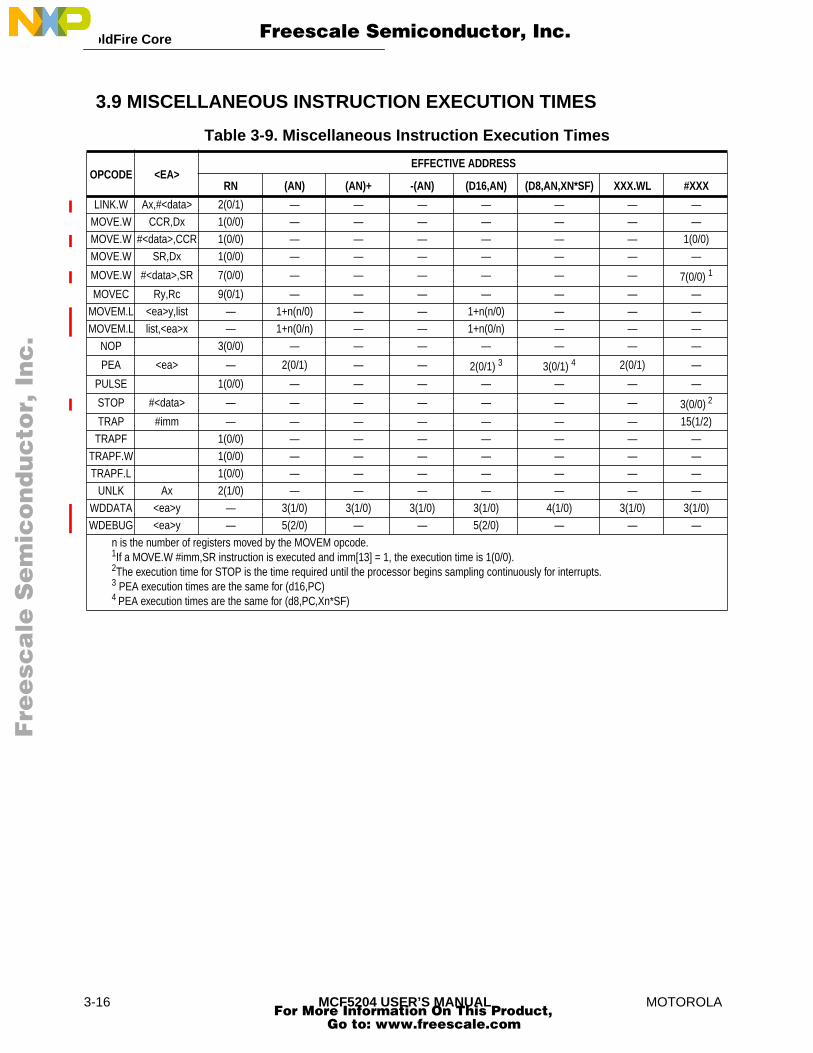
ColdFire Core
F
ree
sca
le S
em
ico
nd
uc
tor,
I
Freescale Semiconductor, Inc.n
c..
.
3.9 MISCELLANEOUS INSTRUCTION EXECUTION TIMES
Table 3-9. Miscellaneous Instruction Execution Times
OPCODE <EA>EFFECTIVE ADDRESS
RN (AN) (AN)+ -(AN) (D16,AN) (D8,AN,XN*SF) XXX.WL #XXX
LINK.W Ax,#<data> 2(0/1) — — — — — — —MOVE.W CCR,Dx 1(0/0) — — — — — — —MOVE.W #<data>,CCR 1(0/0) — — — — — — 1(0/0)MOVE.W SR,Dx 1(0/0) — — — — — — —
MOVE.W #<data>,SR 7(0/0) — — — — — — 7(0/0) 1
MOVEC Ry,Rc 9(0/1) — — — — — — —MOVEM.L <ea>y,list — 1+n(n/0) — — 1+n(n/0) — — —MOVEM.L list,<ea>x — 1+n(0/n) — — 1+n(0/n) — — —
NOP 3(0/0) — — — — — — —
PEA <ea> — 2(0/1) — — 2(0/1) 3 3(0/1) 4 2(0/1) —
PULSE 1(0/0) — — — — — — —
STOP #<data> — — — — — — — 3(0/0) 2
TRAP #imm — — — — — — — 15(1/2)TRAPF 1(0/0) — — — — — — —
TRAPF.W 1(0/0) — — — — — — —TRAPF.L 1(0/0) — — — — — — —
UNLK Ax 2(1/0) — — — — — — —WDDATA <ea>y — 3(1/0) 3(1/0) 3(1/0) 3(1/0) 4(1/0) 3(1/0) 3(1/0)WDEBUG <ea>y — 5(2/0) — — 5(2/0) — — —
n is the number of registers moved by the MOVEM opcode.1If a MOVE.W #imm,SR instruction is executed and imm[13] = 1, the execution time is 1(0/0).2The execution time for STOP is the time required until the processor begins sampling continuously for interrupts.3 PEA execution times are the same for (d16,PC)4 PEA execution times are the same for (d8,PC,Xn*SF)
3-16 MCF5204 USER’S MANUAL MOTOROLA For More Information On This Product,
Go to: www.freescale.com
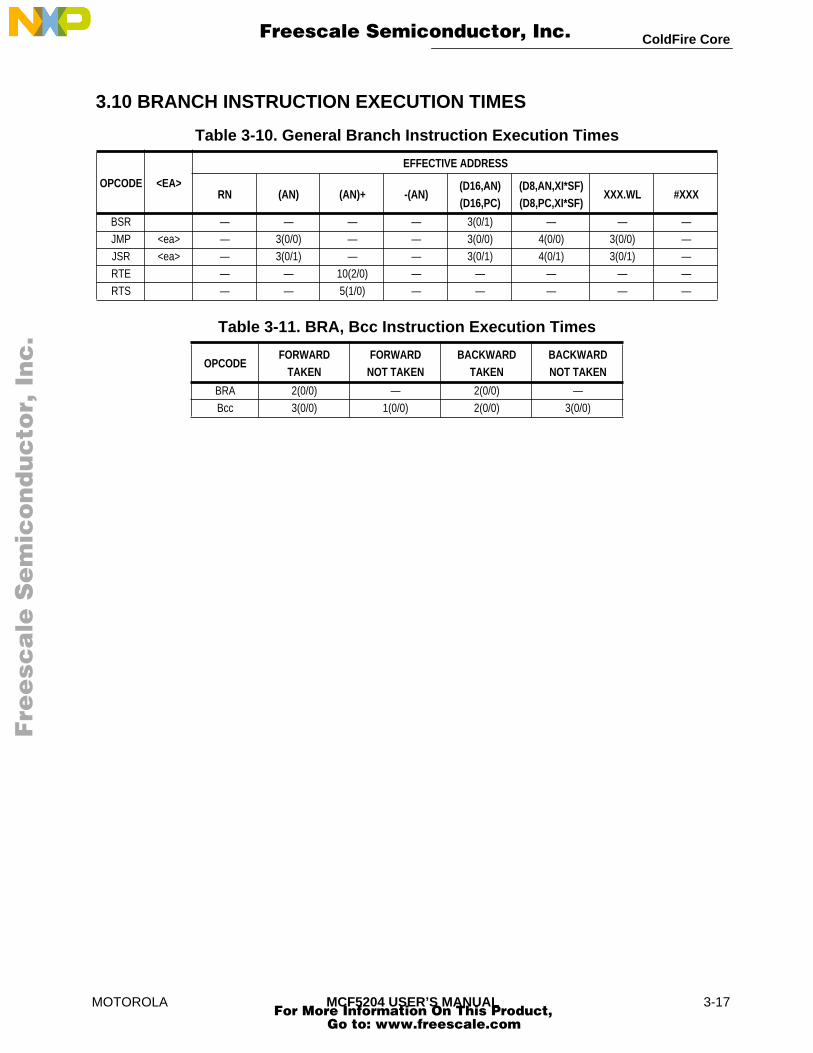
ColdFire Core
F
ree
sca
le S
em
ico
nd
uc
tor,
I
Freescale Semiconductor, Inc.n
c..
.
3.10 BRANCH INSTRUCTION EXECUTION TIMES
Table 3-10. General Branch Instruction Execution Times
OPCODE <EA>
EFFECTIVE ADDRESS
RN (AN) (AN)+ -(AN)(D16,AN)(D16,PC)
(D8,AN,XI*SF) (D8,PC,XI*SF)
XXX.WL #XXX
BSR — — — — 3(0/1) — — —JMP <ea> — 3(0/0) — — 3(0/0) 4(0/0) 3(0/0) —JSR <ea> — 3(0/1) — — 3(0/1) 4(0/1) 3(0/1) —RTE — — 10(2/0) — — — — —RTS — — 5(1/0) — — — — —
Table 3-11. BRA, Bcc Instruction Execution Times
OPCODEFORWARD
TAKENFORWARD
NOT TAKENBACKWARD
TAKENBACKWARDNOT TAKEN
BRA 2(0/0) — 2(0/0) —Bcc 3(0/0) 1(0/0) 2(0/0) 3(0/0)
MOTOROLA MCF5204 USER’S MANUAL 3-17 For More Information On This Product,
Go to: www.freescale.com

DATE: 08-21-98
REVISION NO: 0.1
PAGES AFFECTED: SEE CHANGE BARS
F
ree
sca
le S
em
ico
nd
uc
tor,
I
Freescale Semiconductor, Inc.n
c..
.
SECTION 4INSTRUCTION CACHE
4.1 FEATURES OF INSTRUCTION CACHE• 512 Byte Direct-Mapped Cache
• Single-Cycle Access on Cache Hits
• Physically Located on Processor's High-Speed Local Bus
• Nonblocking Design to Maximize Performance
• 16-Byte Line-Fill Buffer
• Configurable Cache Miss-Fetch Algorithm
4.2 INSTRUCTION CACHE PHYSICAL ORGANIZATIONThe instruction cache is a direct-mapped single-cycle memory, organized as 32 lines, each containing 16 bytes. The memory storage consists of a 32-entry tag array (containing addresses and a valid bit), and the data array containing 512bytes of instruction data, organized as 128 x 32 bits.
The two memory arrays are accessed in parallel: bits [8:4] of the instruction fetch address provide the index into the tag array, and bits [3:2] addressing the data array. The tag array outputs the address mapped to the given cache location along with the valid bit for the line. This address field is compared to bits [31:9] of the instruction fetch address from the local bus to determine if a cache hit in the memory array has occurred. If the desired address is mapped into the cache memory, the output of the data array is driven onto the processor's local data bus completing the access in a single cycle.
The tag array maintains a single valid bit per line entry. Accordingly, only entire 16-byte lines are loaded into the instruction cache.
The instruction cache also contains a 16-byte fill buffer that provides temporary storage for the last line fetched in response to a cache miss. With each instruction fetch, the contents of the line fill buffer are examined. Thus, each instruction fetch address examines both the tag memory array and the line fill buffer to see if the desired address is mapped into either hardware resource. A cache hit in either the memory array or the line-fill buffer is serviced in a single cycle. Because the line fill buffer maintains valid bits on a longword basis, hits in the buffer can be serviced immediately without waiting for the entire line to be fetched.
If the referenced address is not contained in the memory array or the line-fill buffer, the instruction cache initiates the required external fetch operation. In most situations, this is a 16-byte line-sized burst reference.
MOTOROLA MCF5204 USER’S MANUAL 4-1 For More Information On This Product,
Go to: www.freescale.com
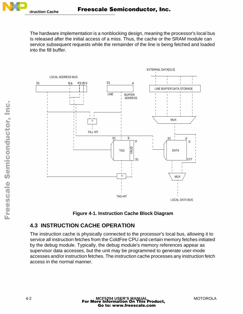
Instruction Cache
4
F
ree
sca
le S
em
ico
nd
uc
tor,
I
Freescale Semiconductor, Inc.n
c..
.
The hardware implementation is a nonblocking design, meaning the processor's local bus is released after the initial access of a miss. Thus, the cache or the SRAM module can service subsequent requests while the remainder of the line is being fetched and loaded into the fill buffer.
Figure 4-1. Instruction Cache Block Diagram
4.3 INSTRUCTION CACHE OPERATIONThe instruction cache is physically connected to the processor's local bus, allowing it to service all instruction fetches from the ColdFire CPU and certain memory fetches initiated by the debug module. Typically, the debug module's memory references appear as supervisor data accesses, but the unit may be programmed to generate user-mode accesses and/or instruction fetches. The instruction cache processes any instruction fetch access in the normal manner.
31 9 8 43 012 31 4
MUX
EXTERNAL DATA[31:0]
LOCAL ADDRESS BUS
LINE BUFFER DATA STORAGE
TAG DATA
MUX
LOCAL DATA BUS
VALI
D
LINE BUFFERADDRESS
=
FILL HIT
=
TAG-HIT
31 9 31 0
‘12731
00
-2 MCF5204 USER’S MANUAL MOTOROLA For More Information On This Product,
Go to: www.freescale.com

Instruction Cache
F
ree
sca
le S
em
ico
nd
uc
tor,
I
Freescale Semiconductor, Inc.n
c..
.
4.3.1 Interaction With Other ModulesBecause both the instruction cache and high-speed SRAM module are connected to the processor's local data bus, certain user-defined configurations can result in simultaneous instruction fetch processing.
If the referenced address is mapped into the SRAM module, that module will service the request in a single cycle. In this case, data accessed from the instruction cache is simply discarded and no external memory references are generated. If the address is not mapped into the SRAM space, the instruction cache handles the request in the normal fashion.
4.3.2 Memory Reference AttributesFor every memory reference generated by the processor or the debug module, a set of “effective attributes” is determined based on the address and the Access Control Registers (ACR0, ACR1). This set of attributes includes the cacheable/noncacheable definition, the precise/imprecise handling of operand write, and the write-protect capability.
In particular, each address is compared to the values programmed in the Access Control Registers (ACR). If the address matches one of the ACR values, the access attributes from that ACR are applied to the reference. If the address does not match either ACR, then the default value defined in the Cache Control Register (CACR) is used. The specific algorithm is as follows:
if (address = ACR0_address including mask) Effective Attributes = ACR0 attributes else if (address = ACR1_address including mask) Effective Attributes = ACR1 attributes else Effective Attributes = CACR default attributes
4.3.3 Cache Coherency and InvalidationThe instruction cache does not monitor processor data references for accesses to cached instructions. Therefore, software must maintain cache coherency by invalidating the appropriate cache entries after modifying code segments.
The cache invalidation can be performed in two ways. The assertion of bit 24 in the CACR forces the entire instruction cache to be marked as invalid. The invalidation operation requires 32 cycles because the cache sequences through the entire tag array, clearing a single location each cycle. Any subsequent instruction fetch accesses are postponed until the invalidation sequence is complete.
The privileged CPUSHL instruction can invalidate a single cache line. When this instruction is executed, the cache entry defined by bits[8:4] of the source address register is invalidated, provided bit 28 of the CACR is cleared.
These invalidation operations may be initiated from the processor or the debug module.
MOTOROLA MCF5204 USER’S MANUAL 4-3 For More Information On This Product,
Go to: www.freescale.com

Instruction Cache
4
F
ree
sca
le S
em
ico
nd
uc
tor,
I
Freescale Semiconductor, Inc.n
c..
.
4.3.4 RESETA hardware reset clears the CACR disabling the instruction cache. The contents of the tag array are not affected by the reset. Accordingly, the system startup code must explicitly perform a cache invalidation by setting CACR[24] before the cache can be enabled.
4.3.5 Cache Miss Fetch Algorithm/Line FillsAs discussed in subsection 5.2, the instruction cache hardware includes a 16-byte line fill buffer for providing temporary storage for the last fetched instruction.
With the cache enabled as defined by CACR[31], a cacheable instruction fetch that misses in both the tag memory and the line-fill buffer generates a external fetch. The size of the external fetch is determined by the value contained in the 2-bit CLNF field of the CACR and the miss address. Table 4-1 shows the relationship between the CLNF bits, the miss address, and the size of the external fetch.
Depending on the runtime characteristics of the application and the memory response speed, overall performance can be increased by programming the CLNF bits to values {00, 01}.
For all cases of a line-sized fetch, the critical longword defined by bits [3:2] of the miss address is accessed first followed by the remaining three longwords that are accessed by incrementing the longword address in a modulo-16 fashion as shown below:
if miss address[3:2] = 00 fetch sequence = {$0, $4, $8, $C} if miss address[3:2] = 01 fetch sequence = {$4, $8, $C, $0} if miss address[3:2] = 10 fetch sequence = {$8, $C, $0, $4} if miss address[3:2] = 11 fetch sequence = {$C, $0, $4, $8}
Once an external fetch has been initiated and the data loaded into the line-fill buffer, the instruction cache maintains a special “most-recently-used” indicator that tracks the contents of the fill buffer versus its corresponding cache location. At the time of the miss, the hardware indicator is set, marking the fill buffer as “most recently used.” If a subsequent access occurs to the cache location defined by bits [8:4] of the fill buffer address, the data in the cache memory array is now most recently used, so the hardware
Table 4-1. Initial Fetch Offset vs. CLNF Bits
CLNF[1:0]LONGWORD ADDRESS BITS
00 01 10 11
00 Line Line Line Longword01 Line Line Longword Longword1X Line Line Line Line
-4 MCF5204 USER’S MANUAL MOTOROLA For More Information On This Product,
Go to: www.freescale.com

Instruction Cache
F
ree
sca
le S
em
ico
nd
uc
tor,
I
Freescale Semiconductor, Inc.n
c..
.
indicator is cleared. In all cases, the indicator defines whether the contents of the line fill buffer or the memory data array are most recently used. At the time of the next cache miss, the contents of the line-fill buffer are written into the memory array if the entire line is present, and the fill buffer data is still most recently used compared to the memory array.
The fill buffer can also be used as temporary storage for line-sized bursts of non-cacheable references under control of CACR[10]. With this bit set, a noncacheable instruction fetch is processed as defined by Table 4-1. For this condition, the fill buffer is loaded and subsequent references can hit in the buffer, but the data is never loaded into the memory array.
The relationship between CACR bits 31 and 10, and the type of instruction fetch is shown below in Table 4-2.
4.4 INSTRUCTION CACHE PROGRAMMING MODELThe operation of the instruction cache and local bus controller are defined by three supervisor registers: the Cache Control Register (CACR) and two Access Control Registers (ACR0, ACR1). All three registers can be written from the processor using the privileged MOVEC instruction. Additionally, the registers can be accessed from the debug module. From the debug module, the registers can be read or written. In all cases, undefined bits in a register are reserved. These bits should be written as zeroes and should return zeroes when read from the debug module.
4.4.1 Cache Control Register (CACR)The operation of the instruction cache is controlled by the CACR. The CACR also provides a set of default memory access attributes used when a reference address does not map into the spaces defined by the ACRs.
The CACR is accessed as control register $002 using the privileged MOVEC instruction. This instruction provides write-only access to this register from the processor.
Table 4-2: Instruction Cache Operation as Defined by CACR[31, 10]
CACR[31] CACR[10] TYPE OF INSTR. FETCH DESCRIPTION
0 0 N/A Instruction cache is completely disabled; all fetches are word, longword in size.
0 1 N/A All fetches are word, longword in size
1 X Cacheable Fetch size is defined by Table 5-1 and contents of the line-fill buffer can be written into the memory array
1 0 Noncacheable All fetches are longword in size, and not loaded into the line-fill buffer
1 1 Noncacheable Fetch size is defined by Table 5-1 and loaded into the line-fill buffer, but are never written into the memory array.
MOTOROLA MCF5204 USER’S MANUAL 4-5 For More Information On This Product,
Go to: www.freescale.com

Instruction Cache
4
F
ree
sca
le S
em
ico
nd
uc
tor,
I
Freescale Semiconductor, Inc.n
c..
.
Additionally, the CACR register can be accessed from the debug module in a similar manner. The entire register is cleared by hardware reset.
4.4.1.1 BIT DEFINITIONS.
4.4.1.1.1 CENB - Cache Enable.
0 = Cache disabled 1 = Cache enabled
When the cache is disabled, all instruction fetches generate word or longword-sized fetches. Generally, longword references are used for sequential fetches. If the processor branches to an odd word address, a word-sized fetch is generated. The memory array of the instruction cache are enabled only if CENB is asserted.
4.4.1.1.2 CPDI - Disable CPUSHL Invalidation.
0 = Enable invalidation1 = Disable invalidation
When the privileged CPUSHL instruction is executed, the cache entry defined by bits [8:4] of the address is invalidated if CPDI = 0. If CPDI = 1, no operation is performed.
4.4.1.2 CFRZ - CACHE FREEZE.
0 = Normal operation1 = Freeze valid cache lines
Setting this bit effectively freezes the cache contents. Line fetches can still be initiated and loaded into the line-fill buffer, but a valid cache entry is never overwritten. If a given cache location is invalid, the contents of the line-fill buffer can be written into the memory array while CFRZ is asserted.
CENB - - CPDI CFRZ - - CINV - - - - - - - -
31 30 29 28 27 26 25 24 23 22 21 20 19 18 17 16
RESET:
- - - - - CEIB DCM DBWE - - DWP - - - CLNF1 CLNF0
15 14 13 12 11 10 9 8 7 6 5 4 3 2 1 0
0 0 0 0 0 0 0 0 0 0 0 0 0 0 0 0RESET:
0 0 0 0 0 0 0 0 0 0 0 0 0 0 0 0
-6 MCF5204 USER’S MANUAL MOTOROLA For More Information On This Product,
Go to: www.freescale.com

Instruction Cache
F
ree
sca
le S
em
ico
nd
uc
tor,
I
Freescale Semiconductor, Inc.n
c..
.
4.4.1.3 CINV - CACHE INVALIDATE.
0 = No operation1 = Invalidate all cache locations
Setting this bit forces the cache to invalidate each tag array entry. The invalidation process requires 32 machine cycles, with a single cache entry cleared per machine cycle. The state of this bit is always read as a zero. After a hardware reset, the cache must be invalidated before it is enabled.
4.4.1.4 CEIB - CACHE ENABLE NONCACHEABLE INSTRUCTION BURSTING.
0 = Disable burst fetches on noncacheable accesses1 = Enable burst fetches on noncacheable accesses
Setting this bit allows the line-fill buffer to be loaded with burst transfers under control of CLNF[1:0] for noncacheable accesses. Noncacheable accesses are never written into the memory array.
4.4.1.5 DCM - DEFAULT CACHE MODE.
0 = Caching enabled1 = Caching disabled
This bit defines the default cache mode: 0 is cacheable, 1 is noncacheable. For more information on the selection of the effective memory attributes, see subsection 5.3.2.
4.4.1.6 DBWE - DEFAULT BUFFERED WRITE ENABLE.
0 = Disable buffered writes1 = Enable buffered writes
This bit defines the default value for enabling buffered writes. If DBWE = 0, the termination of an operand write cycle on the processor's local bus is delayed until the external bus cycle is completed. If DBWE = 1, the write cycle on the local bus is terminated immediately and the operation buffered in the bus controller. In this mode, operand write cycles are effectively decoupled between the processor's local bus and the external bus.
Generally, the enabling of buffered writes provides higher system performance but recovery from access errors may be more difficult. For the ColdFire CPU, the reporting of access errors on operand writes is always imprecise and enabling buffered writes simply decouples the write instruction from the signaling of the fault even more.
4.4.1.7 DWP - DEFAULT WRITE PROTECTION.
0 = Read and write accesses permitted1 = Only read accesses permitted
MOTOROLA MCF5204 USER’S MANUAL 4-7 For More Information On This Product,
Go to: www.freescale.com

Instruction Cache
4
F
ree
sca
le S
em
ico
nd
uc
tor,
I
Freescale Semiconductor, Inc.n
c..
.
4.4.1.8 CLNF[1:0] - CACHE LINE FILL.
These bits control the size of the memory request the cache issues to the bus controller for different initial line access offsets.
4.5 ACCESS CONTROL REGISTERS
4.6 FEATURES The two ACRs provide a definition of memory reference attributes for two memory regions (one per ACR). This set of effective attributes is defined for every memory reference using the ACRs or the set of default attributes contained in the CACR. The ACRs are examined for every memory reference that is NOT mapped to the SRAM module.
4.7 ACR PROGRAMMING MODELThe ACRs are accessed as control registers $004 and $005 using the privileged MOVEC instruction (ACR0 = $004, ACR1 = $005). This instruction provides write-only access to these registers from the processor. Additionally, the ACRs may be accessed from the debug module in a similar manner. Each ACR is disabled by a hardware reset.
4.7.1 Access Control Registers (ACR0,ACR1)
Table 4-3. External Fetch Size Based on Miss Address and CLNF
CLNF[1:0]LONGWORD ADDRESS BITS
00 01 10 11
00 Line Line Line Longword01 Line Line Longword Longword1X Line Line Line Line
AB31 AB30 AB29 AB28 AB27 AB26 AB25 AB24 AM31 AM30 AM29 AM28 AM27 AM26 AM25 AM24
31 30 29 28 27 26 25 24 23 22 21 20 19 18 17 16
0 0 0 0 0 0 0 0 0 0 0 0 0 0 0 0RESET:
EN SM1 SM0 - - - - - - CM BUFW - - WP - -
15 14 13 12 11 10 9 8 7 6 5 4 3 2 1 0
0 0 0 0 0 0 0 0 0 0 0 0 0 0 0 0RESET:
-8 MCF5204 USER’S MANUAL MOTOROLA For More Information On This Product,
Go to: www.freescale.com
Instruction Cache
F
ree
sca
le S
em
ico
nd
uc
tor,
I
Freescale Semiconductor, Inc.n
c..
.
4.7.1.1 AB[31:24] - ADDRESS BASE [31:24].
This 8-bit field is compared to address bits [31:24] from the processor's local bus under control of the ACR address mask. If the address matches, the attributes for the memory reference are sourced from the given ACR.
4.7.1.2 AM[23:16] - ADDRESS MASK [23:16].
This 8-bit field can mask any bit of the AB field comparison. If a bit in the AM field is set, then the corresponding bit of the address field comparison is ignored.
4.7.1.3 EN - ENABLE.
0 = ACR disabled1 = ACR enabled
The EN bit defines the ACR enable. Hardware reset clears this bit, disabling the ACR.
4.7.1.4 SM[1:0] - SUPERVISOR MODE.
00 = Match if user mode01 = Match if supervisor mode1x = Match always - ignore user/supervisor mode
This two-bit field allows the given ACR to be applied to references based on operating privilege mode of the ColdFire processor. The field uses the ACR for user references only, supervisor references only, or all accesses.
4.7.1.5 CM - CACHE MODE.
0 = Caching enabled1 = Caching disabled
This bit defines the cache mode: 0 is cacheable, 1 is noncacheable.
4.7.1.6 BWE- BUFFERED WRITE ENABLE.
0 = Don’t buffer writes1 = Buffer writes
This bit defines the value for enabling buffered writes. If BWE = 0, the termination of an operand write cycle on the processor's local bus is delayed until the external bus cycle is completed. If BWE = 1, the write cycle on the local bus is terminated immediately and the operation is then buffered in the bus controller. In this mode, operand write cycles are effectively decoupled between the processor's local bus and the external bus.
Generally, the enabling of buffered writes provides higher system performance but recovery from access errors may be more difficult. For the ColdFire CPU, the reporting of
MOTOROLA MCF5204 USER’S MANUAL 4-9 For More Information On This Product,
Go to: www.freescale.com

Instruction Cache
4
F
ree
sca
le S
em
ico
nd
uc
tor,
I
Freescale Semiconductor, Inc.n
c..
.
access errors on operand writes is always imprecise, and enabling buffered writes simply decouples the write instruction from the signaling of the fault even more.
4.7.1.7 WP - WRITE PROTECT.
0 = Read and write accesses permitted1 = Only read accesses
The WP bit defines the write-protection attribute. If the effective memory attributes for a given access select the WP bit, any attempted write with this bit set is terminated with an access error.
-10 MCF5204 USER’S MANUAL MOTOROLA For More Information On This Product,
Go to: www.freescale.com
DATE: 08-21-98
REVISION NO: 0.1
PAGES AFFECTED: SEE CHANGE BARS
F
ree
sca
le S
em
ico
nd
uc
tor,
I
Freescale Semiconductor, Inc.n
c..
.
SECTION 5SRAM
5.1 SRAM FEATURES• 512 Byte SRAM, Organized as 128 x 32 Bits
• Single-Cycle Access
• Physically Located on Processor's High-Speed Local Bus
• Byte, Word, Longword Address Capabilities
• Memory Mapping Defined by the Customer
5.2 SRAM OPERATIONThe SRAM module provides a general-purpose memory block that the ColdFire CPU can access in a single cycle. The location of the memory block can be specified to any 0-modulo-512 address within the four gigabyte address space. The memory is ideal for storing critical code or data structures or for use as the system stack. Because the SRAM module is physically connected to the processor's high-speed local bus, it can service CPU-initiated accesses or memory-referencing commands from the Debug module.
Depending on configuration information, instruction fetches can be sent to both the instruction cache and the SRAM block simultaneously. If the instruction fetch address is mapped into the region defined by the SRAM, the SRAM provides the data back to the processor, and the I-Cache data discarded. Accesses from the SRAM module are not cached.
5.3 SRAM PROGRAMMING MODELThe configuration information in the SRAM Base Address Register (RAMBAR) controls the operation of the SRAM module. The RAMBAR is accessed as control register $C04 using the privileged MOVEC instruction. The MOVEC instruction provides write-only access to this register. Additionally, the RAMBAR register can be accessed from the Debug module in a similar manner. From the Debug module, the register can be read or written. All undefined bits in the register are reserved. These bits should be written as zeroes, and return zeroes when read from the debug module. Only the valid bit is cleared by a hardware reset.
MOTOROLA MCF5204 USER’S MANUAL 5-1 For More Information On This Product,
Go to: www.freescale.com

SRAM
F
ree
sca
le S
em
ico
nd
uc
tor,
I
Freescale Semiconductor, Inc.n
c..
.
5.3.1 SRAM Base Address RegisterThe RAMBAR register contains four control fields. These fields are detailed in the following sections. The next illustration is that of the SRAM Base Address Register (SRAMBAR).
5.3.1.1 BA[31:9] - BASE ADDRESS. This field, specified by RAMBAR[31:9], defines the 0-modulo-512 base address for the SRAM module. By programming this field, the SRAM can be located anywhere within the four gigabyte ColdFire address space.
5.3.1.2 WP[8] - WRITE PROTECT. The write-protect field is defined by RAMBAR[8]. If set, this bit allows only read accesses to the SRAM. Any attempted write access will generate an access error exception in the processor.
If cleared, the SRAM supports read and write references. If WP = 0, SRAM supports read and write accesses. If WP = 1, SRAM supports only read accesses. Attempted writes generate access errors.
5.3.1.3 AS[7:1] - ADDRESS SPACE MASKS. This five-bit field, specified by RAMBAR[7:1], allows certain types of accesses to be “masked,” or inhibited, from accessing the SRAM module. The mask bits are defined as:
• AS5 - Mask CPU Space and Interrupt Acknowledge Accesses
• AS4 - Mask Supervisor Code Accesses
• AS3 - Mask Supervisor Data Accesses
• AS2 - Mask User Code Accesses
• AS1 - Mask User Data Accesses
If a given mask bit is set, references of that type are not allowed to access the SRAM module. These bits are useful for power management as detailed in subsection 5.3.3.
If ASn = 0, accesses of the given type are allowed by the SRAM. If ASn = 1, accesses of the given type are not allowed by the SRAM.
BA31 BA30 BA29 BA28 BA27 BA26 BA25 BA24 BA23 BA22 BA21 BA20 BA19 BA18 BA17 BA16
31 30 29 28 27 26 25 24 23 22 21 20 19 18 17 16
- - - - - - - - - - - - - - - -RESET:
BA15 BA14 BA13 BA12 BA11 BA10 BA9 WP AS7 AS6 AS5 AS4 AS3 AS2 AS1 V
15 14 13 12 11 10 9 8 7 6 5 4 3 2 1 0
- - - - - - - - - - - - - - - 0RESET:
5-2 MCF5204 USER’S MANUAL MOTOROLA For More Information On This Product,
Go to: www.freescale.com

SRAM
F
ree
sca
le S
em
ico
nd
uc
tor,
I
Freescale Semiconductor, Inc.n
c..
.
5.3.1.4 V - VALID. The valid bit (V-bit) is specified by RAMBAR[0]. A hardware reset clears this bit. When set, this bit enables the SRAM module; otherwise, the module is disabled.
The mapping of a given access into the SRAM uses the following algorithm to determine if the access “hits” in the memory:
if (RAMBAR[0] = 1) if (requested address[31:9] = RAMBAR[31:9]) if (ASn of the requested type = 0) Access is mapped to the SRAM module if (access = read) Read the SRAM and return the data if (access = write) if (RAMBAR[8] = 0) Write the data into the SRAM else Signal a write-protect access error
5.3.2 SRAM InitializationAfter a hardware reset, the contents of the SRAM module are undefined. The valid bit of the RAMBAR is cleared, disabling the module. If the SRAM needs to be initialized with instructions or data, customers should perform the following steps:
1. Load the RAMBAR mapping the SRAM module to the desired location within the address space.
2. Read the source data and write it to the SRAM. There are various instructions to support this function, including memory-to-memory move instructions, or the MOVEM opcode. The MOVEM instruction is optimized to generate line-sized burst fetches on 0-modulo-16 addresses, so this opcode generally provides maximum performance.
3. After the data has been loaded into the SRAM, it may be appropriate to load a revised value into the RAMBAR with a new set of “attributes.” These attributes consist of the write-protect and address space mask fields.
The ColdFire processor or an external emulator using the Debug module can perform these initialization functions.
5.3.3 Power ManagementAs noted previously, depending on the configuration defined by the RAMBAR, instruction fetch accesses can be sent to the SRAM module and the I-Cache simultaneously. If the access is mapped to the SRAM module, it sources the read data, discarding the I-Cache access. If the SRAM is used only for data operands, power dissipation can be lowered by asserting the ASn bits associated with instruction fetches. Additionally, if the SRAM contains only instructions, power dissipation can be reduced by masking operand accesses.
MOTOROLA MCF5204 USER’S MANUAL 5-3 For More Information On This Product,
Go to: www.freescale.com

SRAM
F
ree
sca
le S
em
ico
nd
uc
tor,
I
Freescale Semiconductor, Inc.n
c..
.
Consider the examples on Table 5-1 of typical RAMBAR settings:
Table 5-1. Examples of Typical RAMBAR Settings
DATA CONTAINED IN SRAM RAMBAR[7:0]
Code only $2BData only $35
Both Code and Data $21
5-4 MCF5204 USER’S MANUAL MOTOROLA For More Information On This Product,
Go to: www.freescale.com
DATE: 08-21-98
REVISION NO: 0.1
PAGES AFFECTED: SEE CHANGE BARS
F
ree
sca
le S
em
ico
nd
uc
tor,
I
Freescale Semiconductor, Inc.n
c..
.
SECTION 6BUS OPERATION
The MCF5204 bus interface supports both asynchronous/synchronous and sized/bursted data transfers between the processor and other devices in the system.
This section describes the bus functionality, the signals that control the bus, and the bus cycles provided for data transfer operations. The waveforms illustrate the bus activity for an MCF5204 processor. Description of the reset operation is also included.
6.1 BUS AND CONTROL SIGNALS
6.1.1 Address BusThe address bus signals are outputs that define the address of the byte (or most significant byte) to be transferred during a bus cycle. The MCF5204 places the address on the bus at the beginning of a bus cycle. The address is valid while CS is asserted. During an interrupt acknowledge access, the lower address lines, A4-A2, indicate the interrupt level being acknowledged.
6.1.2 Data BusThis bidirectional, nonmultiplexed, parallel bus contains the data being transferred to or from the MCF5204. Data is latched on the bus on the rising clock edge. A read or write operation can transfer 8 or 16 bits of data (one or two bytes) in one bus cycle. For a write cycle, all 16 bits of the data bus are driven, regardless of the port width or operand size.
6.1.3 Chip-SelectThe chip-select output signals enable peripherals at programmed addresses. Each chip-select can be programmed for an address location as well as for masking capabilities, port size, bursting, wait-state generation, and internal/external termination. A reset disables these chip-selects.
6.1.4 ATSAddress transition start (ATS), an active-low signal, indicates that an address transition has occurred and that a decode of the address can start at the next rising clock edge. This signal is used primarily with programmable logic that latches inputs on the rising edge of the clock. This signal provides an early indication to external logic that a bus cycle is starting, which saves a clock since logic does not need to wait an additional CLK for CS signals and bus strobes to be asserted.
MOTOROLA MCF5204 USER’S MANUAL 6-1 For More Information On This Product,
Go to: www.freescale.com

Bus Operation
F
ree
sca
le S
em
ico
nd
uc
tor,
I
Freescale Semiconductor, Inc.n
c..
.
6.1.5 RE - Read EnableThis active-low output indicates that the MCF5204 is ready to read the data. The external peripheral or memory should enable the data out while RE is asserted.
6.1.6 WE - Write EnableThis active-low output signal indicates the direction of a data transfer on the data bus. A logic one indicates a read from a slave device; a logic zero indicates a write to a slave device.
6.1.7 Byte Write Enables / Byte Data StrobesThe MCF5204 supports two modes of operation for the byte enables. These two modes are the write-enable mode (UWE/LWE) and the data-strobe mode (UDS/LDS). The mode can be configured for each chip-select address space and is controlled by programming a control bit in each Chip-Select Control Register.
These two modes provide maximum flexibility when selecting and interfacing to various external memory devices. Burst accesses must meet the following criteria:
• Internal termination
• Read
• Transfer size must exceed port size
• Burst access enabled in chip-select configuration register
6.1.7.1 BYTE WRITE-ENABLE MODE. When configured for write-enable mode, the byte enables assert only on write accesses.
6.1.7.2 BYTE DATA-STROBE MODE. When configured for data-strobe mode, the byte enables assert on both read and write accesses.
6.1.7.3 BYTE ENABLE OPERATION. On a write to a 16-bit port, these active-low output signals indicate when the upper or lower eight bits of the data bus contain valid data. The upper write enable indicates that the upper eight bits of the data bus contain valid data during a write cycle.The lower write enable indicates that the lower eight bits of the data bus contain valid data during a write cycle.
In 8-bit wide bus-port size (programmed in conjunction with chip-selects), all bus cycles appear as 8-bit reads or writes to the upper half of the data bus (D[15:8]), and so only UWE/UDS is asserted. A0 should be used to determine the even or odd byte being addressed in this case; it is valid whenever the external CS signal is asserted during such a cycle. There is no external indication of data bus width other than the chip-select asserted. You know what bus width that chip-select is programmed to provide for any given configuration of the MCF5204 in a system.
6-2 MCF5204 USER’S MANUAL MOTOROLA For More Information On This Product,
Go to: www.freescale.com

Bus Operation
F
ree
sca
le S
em
ico
nd
uc
tor,
I
Freescale Semiconductor, Inc.n
c..
.
6.1.8 DTACK This active-low input signal allows asynchronous data transfers between the MCF5204 and external devices. During bus cycles, external devices can assert DTACK as part of the bus protocol. During a read cycle, this signal indicates to the MCF5204 to terminate the bus cycle and to latch the data. During a write cycle, this signal indicates that the external device has successfully stored the data and that the cycle can terminate during a reset cycle. During a read cycle, data is latched one clock after assertion of DTACK because of the time required to internally synchronize this signal. DTACK must be driven for one full clock to ensure that the MCF5204 properly synchronizes the signal.
External termination is selected as a programming option in the Chip-Select Control Register.
6.2 DIRECT CONNECTION BUS INTERFACEThe MCF5204 provides a direct connection (i.e., glueless) interface to most standard RAM, ROM, and FLASH devices that are currently on the market. The interface is glue- less in that no external glue logic is required to interface the MCF5204 to external memories. The control strobes are all designed to interface directly to standard memories.
Two features that make the MCF5204 bus well-suited to provide a glueless interface are the byte enables and inclusion of both WE and RE control strobes.
The MCF5204 offers two modes of functionality for byte enables that allow you to select between write enables or data-strobe enables. The default mode, write enables, is designed for standard SRAM, ROM, and FLASH parts that have CE, WE, and OE pins. All chip-selects use this default mode after reset. Certain other SRAMS have data-strobe enables that must be asserted during reads as well as writes. To accommodate these SRAMS, another mode of byte enable can be invoked by setting the BEM bit in the relevant chip-select address register to activate the upper and lower data strobes.
With both WE and RE, WE normally take the place of the R/W signal commonly found on many embedded processors. RE is a complementary signal to WE (but WE and RE are not simple inversions of each other) and is included for a glueless interface to some memory devices. Most memories do not specify a value for the RE input during write cycles, allowing you to connect the CS output to the RE input where the value of RE is specified for all uses. There are exceptions, typically with flash memories. The RE signal allows a glueless interface to these devices without any external logic.
6.3 WAIT STATESThe MCF5204 allows the automatic insertion of wait states, if required. Each individual chip-select programs the wait states.
Zero wait-state operation should be used for clock frequencies at or below 16MHz. At higher frequencies, zero wait-state operation requires very fast SRAM, if operation is possible at all.
MOTOROLA MCF5204 USER’S MANUAL 6-3 For More Information On This Product,
Go to: www.freescale.com

Bus Operation
F
ree
sca
le S
em
ico
nd
uc
tor,
I
Freescale Semiconductor, Inc.n
c..
.
6.4 PORT SIZINGThe MCF5204 supports read and writes to ports of various sizes. The MCF5204 supports read and writes to both byte (8 bit) and word (16 bit) port sizes. Devices that present a byte-sized port must be connected to the upper byte of the data bus (DATA[15:8]).
6.5 BURSTING OPERATIONBursting operation is enabled as a programming option in the Chip-Select Control Register. Each chip-select space can be individually programmed for bursting or non-bursting. When the bus operation meets the criteria for a burst to occur but bursting is not enabled in the Chip-Select Control Register, a burst-inhibited bus transfer results.
Bursted access normally occurs only to SRAM or ROM. Bursted access does not negate the chip-select or read enable between access; only the address field changes. Bursted accesses complete faster than normal accesses, resulting in increased performance, especially with respect to cache line fills.
Bursting can occur on any access where the size of the memory operand is greater than the port size (i.e. LW to W, W to B, any line sized access). Bursting access will occur only on read accesses, with internal termination.
Burst mode supports programmable wait states. External termination will terminate any bus cycle, including burst cycles.
Because there is a minimum of two clocks per bus cycle, there is no advantage to bursting with zero wait states.
6.6 BUS EXCEPTIONS
6.6.1 IACKIACK bus cycles can be indicated externally by programming a Chip-select Control Register to respond to only CPU/IACK accesses with a CSAR value of $FFFFFExx.
6.6.2 Bus ErrorsThere is no support for external bus errors. The MCF5204 can cause an internal bus error by a timeout of the internal bus monitor.
6.6.3 HaltThere is no support for an external halt.
6.6.4 Double Bus FaultIf the MCF5204 experiences a double bus fault, it will enter the halted state. To exit the halt state, you should reset the processor.
6-4 MCF5204 USER’S MANUAL MOTOROLA For More Information On This Product,
Go to: www.freescale.com

Bus Operation
F
ree
sca
le S
em
ico
nd
uc
tor,
I
Freescale Semiconductor, Inc.n
c..
.
6.7 BUS CHARACTERISTICSThe MCF5204 processor uses a single clock signal (CLK) to generate its internal clocks as well as the bus clock. Therefore, the external bus operates at the same speed as the processor’s internal clock rate, where all bus operations are synchronous to the rising edge of CLK, and the bus control signals are synchronous to the falling edge of the CLK.
Figure 6-1. Signal Relationships to CLK
The following figures are included in this section1.
1. All of the timing diagrams assume UWE/UDS and LWE/LDS to be programmed as data strobes.
CLK
OUTPUT
SIGNALS
CONTROL
OUTPUT
INPUTS
tvo tho
tvo tho
tsi thi
tvo = PROPAGATION DELAY OF SIGNAL RELATIVE TO CLK EDGE
tho = OUTPUT HOLD TIME RELATIVE TO CLK EDGE
tsi = REQUIRED INPUT SETUP TIME RELATIVE TO CLK EDGE
thi = REQUIRED INPUT HOLD TIME RELATIVE TO CLK EDGE
SIGNALS
MOTOROLA MCF5204 USER’S MANUAL 6-5 For More Information On This Product,
Go to: www.freescale.com

Bus Operation
F
ree
sca
le S
em
ico
nd
uc
tor,
I
Freescale Semiconductor, Inc.n
c..
.
• Figure 6-1; Signal Relationships to CLK
• Figure 6-2; Read: Word, Word Port, External Termination, “1” Wait State
• Figure 6-3; Read: Word, Word Port, External Termination, “2” Wait State
• Figure 6-4; Write: Word, Word Port, External Termination, “1” Wait State
• Figure 6-5; Write: Word, Word Port, External Termination, “2” Wait State
• Figure 6-6; Read: Word, Word Port, Internal Termination, “0” Wait State
• Figure 6-7; Read: Word, Word Port, Internal Termination, “1” Wait State
• Figure 6-8; Read: Word, Word Port, Internal Termination, “2” Wait State
• Figure 6-9; Write: Word, Word Port, Internal Termination, “0” Wait State
• Figure 6-10; Write: Word, Word Port, Internal Termination, “1” Wait State
• Figure 6-11; Write: Word, Word Port, Internal Termination, “2” Wait State
• Figure 6-12; Read: Byte, Word Port, Internal Termination, “0” Wait State
• Figure 6-13; Write: Byte, Word Port, Internal Termination, “0” Wait State
• Figure 6-14; Read/Write: Word, Word Port, Internal Termination, “0” Wait State
• Figure 6-15; Read: Word, Byte Port, Internal Termination, Burst-Inhibited, “0” Wait State
• Figure 6-16; Read: Word, Byte Port, Internal Termination, Burst-Inhibited, “1” Wait State
• Figure 6-17; Read: Word, Byte Port, Internal Termination, Burst-Enabled, “0” Wait State
• Figure 6-18; Read: Word, Byte Port, Internal Termination, Burst-Enabled, “1” Wait State
• Figure 6-19; Write: Word, Byte Port, Internal Termination, “0” Wait State
• Figure 6-20; Write: Word, Byte Port, Internal Termination, “1” Wait State
• Figure 6-21; Read: Line, Word Port, Internal Termination, Burst-Inhibited, “0” Wait State
• Figure 6-22; Read: Line, Word Port, Internal Termination, Burst-Inhibited, “1” Wait State
• Figure 6-23; Read: Line, Word Port, Internal Termination, Burst-Enabled, “0” Wait State
• Figure 6-24; Read: Line, Word Port, Internal Termination, Burst-Enabled, “1” Wait State
• Figure 6-25; Write: Line, Word Port, Internal Termination, “0” Wait State
• Figure 6-26; Write: Line, Word Port, Internal Termination, “1” Wait State
• Figure 6-27; IACK: External Termination, “1” Wait State
• Figure 6-28; IACK: Internal Termination, “0” Wait State
• Figure 6-29; IACK: Internal Termination, “1” Wait State
• Figure 6-30; IACK: Autovector
• Figure 6-31; Reset Operation
6-6 MCF5204 USER’S MANUAL MOTOROLA For More Information On This Product,
Go to: www.freescale.com

Bus Operation
F
ree
sca
le S
em
ico
nd
uc
tor,
I
Freescale Semiconductor, Inc.n
c..
.
Figure 6-2. Read: Word, Word Port, External Termination, “1” Wait State
NOTES:
1. DTACK must be asserted for at least one clock period.
2. This figure depicts the earliest possible external termination (one wait state).
3. Data is latched on the last positive edge of the system clock before CS is negated.
ATS
ADDR
CSx
RE
WE
DATA
DTACK
CLK
UWE/UDS
LWE/LDS
WAIT STATE DATA LATCHED
MOTOROLA MCF5204 USER’S MANUAL 6-7 For More Information On This Product,
Go to: www.freescale.com

Bus Operation
F
ree
sca
le S
em
ico
nd
uc
tor,
I
Freescale Semiconductor, Inc.n
c..
.
Figure 6-3. Read: Word, Word Port, External Termination, “2” Wait State
NOTES:
1. DTACK must be asserted for at least one clock period.
2. This figure depicts DTACK held off for one clock to provide two wait state external termination.
3. Data is latched on the last positive edge of the system clock before the negation of CSx.
ATS
ADDR
CSx
RE
WE
DATA
DTACK
CLK
UWE/UDS
LWE/LDS
WAIT STATE DATA LATCHED
6-8 MCF5204 USER’S MANUAL MOTOROLA For More Information On This Product,
Go to: www.freescale.com

Bus Operation
F
ree
sca
le S
em
ico
nd
uc
tor,
I
Freescale Semiconductor, Inc.n
c..
.
Figure 6-4. Write: Word, Word Port, External Termination, “1” Wait State
NOTES:
1. DTACK must be asserted for at least 1 clock period.
2. This figure depicts the earliest possible external termination (1 wait state).
ATS
ADDR
CSx
RE
WE
DATA
DTACK
CLK
UWE/UDS
LWE/LDS
WAIT STATE
MOTOROLA MCF5204 USER’S MANUAL 6-9 For More Information On This Product,
Go to: www.freescale.com

Bus Operation
F
ree
sca
le S
em
ico
nd
uc
tor,
I
Freescale Semiconductor, Inc.n
c..
.
Figure 6-5. Write: Word, Word Port, External Termination, “2” Wait State
NOTES:
1. DTACK must be asserted for at least one clock period.
2. This figure depicts DTACK held off for one clock to provide two wait state external termination.
ATS
ADDR
CSx
RE
WE
DATA
DTACK
CLK
UWE/UDS
LWE/LDS
WAIT STATE
6-10 MCF5204 USER’S MANUAL MOTOROLA For More Information On This Product,
Go to: www.freescale.com

Bus Operation
F
ree
sca
le S
em
ico
nd
uc
tor,
I
Freescale Semiconductor, Inc.n
c..
.
6.8 READ AND WRITE CYCLES WITH INTERNAL TERMINATION
Figure 6-6. Read: Word, Word Port, Internal Termination, “0” Wait State
NOTES:
1. DATA is latched on the last positive edge of system clock prior to the negation of CSx.
2. This figure shows the earliest possible termination of an external read cycle.
ATS
ADDR
CSx
RE
WE
DATA
DTACK
CLK
UWE/UDS
LWE/LDS
DATA LATCHED
MOTOROLA MCF5204 USER’S MANUAL 6-11 For More Information On This Product,
Go to: www.freescale.com
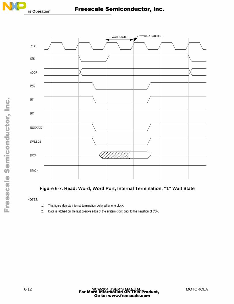
Bus Operation
F
ree
sca
le S
em
ico
nd
uc
tor,
I
Freescale Semiconductor, Inc.n
c..
.
Figure 6-7. Read: Word, Word Port, Internal Termination, “1” Wait State
NOTES:
1. This figure depicts internal termination delayed by one clock.
2. Data is latched on the last positive edge of the system clock prior to the negation of CSx.
ATS
ADDR
CSx
RE
WE
DATA
DTACK
CLK
UWE/UDS
LWE/LDS
WAIT STATE DATA LATCHED
6-12 MCF5204 USER’S MANUAL MOTOROLA For More Information On This Product,
Go to: www.freescale.com
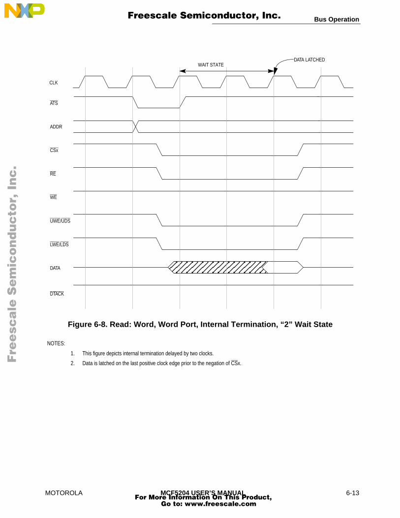
Bus Operation
F
ree
sca
le S
em
ico
nd
uc
tor,
I
Freescale Semiconductor, Inc.n
c..
.
Figure 6-8. Read: Word, Word Port, Internal Termination, “2” Wait State
NOTES:
1. This figure depicts internal termination delayed by two clocks.
2. Data is latched on the last positive clock edge prior to the negation of CSx.
ATS
ADDR
CSx
RE
WE
DATA
DTACK
CLK
UWE/UDS
LWE/LDS
WAIT STATEDATA LATCHED
MOTOROLA MCF5204 USER’S MANUAL 6-13 For More Information On This Product,
Go to: www.freescale.com

Bus Operation
F
ree
sca
le S
em
ico
nd
uc
tor,
I
Freescale Semiconductor, Inc.n
c..
.
Figure 6-9. Write: Word, Word Port, Internal Termination, “0” Wait State
NOTE:
1. This figure depicts the earliest possible internal termination.
ATS
ADDR
CSx
RE
WE
DATA
DTACK
CLK
UWE/UDS
LWE/LDS
6-14 MCF5204 USER’S MANUAL MOTOROLA For More Information On This Product,
Go to: www.freescale.com

Bus Operation
F
ree
sca
le S
em
ico
nd
uc
tor,
I
Freescale Semiconductor, Inc.n
c..
.
Figure 6-10. Write: Word, Word Port, Internal Termination, “1” Wait State
NOTE:
1. This figure depicts internal termination delayed for one clock (1 wait state).
ATS
ADDR
CSx
RE
WE
DATA
DTACK
CLK
UWE/UDS
LWE/LDS
WAIT STATE
MOTOROLA MCF5204 USER’S MANUAL 6-15 For More Information On This Product,
Go to: www.freescale.com

Bus Operation
F
ree
sca
le S
em
ico
nd
uc
tor,
I
Freescale Semiconductor, Inc.n
c..
.
Figure 6-11. Write: Word, Word Port, Internal Termination, “2” Wait State
NOTE:
1. This figure depicts internal termination delayed for two clocks (2 wait states).
ATS
ADDR
CSx
RE
WE
DATA
DTACK
CLK
UWE/UDS
LWE/LDS
WAIT STATE
6-16 MCF5204 USER’S MANUAL MOTOROLA For More Information On This Product,
Go to: www.freescale.com

Bus Operation
F
ree
sca
le S
em
ico
nd
uc
tor,
I
Freescale Semiconductor, Inc.n
c..
.
Figure 6-12. Read: Byte, Word Port, Internal Termination, “0” Wait State
NOTES:
1. This figure depicts the earliest possible internal termination of a read cycle.
2. The even-address access asserts UWE/UDS.
ATS
ADDR
CSx
RE
WE
DATA[15:8]
DTACK
CLK
UWE/UDS
LWE/LDS
$XXXXXXX0
MOTOROLA MCF5204 USER’S MANUAL 6-17 For More Information On This Product,
Go to: www.freescale.com
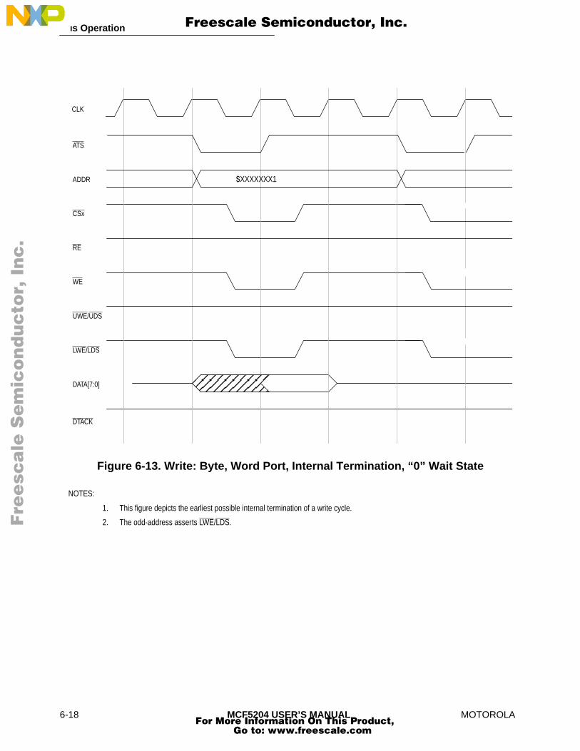
Bus Operation
F
ree
sca
le S
em
ico
nd
uc
tor,
I
Freescale Semiconductor, Inc.n
c..
.
Figure 6-13. Write: Byte, Word Port, Internal Termination, “0” Wait State
NOTES:
1. This figure depicts the earliest possible internal termination of a write cycle.
2. The odd-address asserts LWE/LDS.
ATS
ADDR
CSx
RE
WE
DATA[7:0]
DTACK
CLK
UWE/UDS
LWE/LDS
$XXXXXXX1
6-18 MCF5204 USER’S MANUAL MOTOROLA For More Information On This Product,
Go to: www.freescale.com

Bus Operation
F
ree
sca
le S
em
ico
nd
uc
tor,
I
Freescale Semiconductor, Inc.n
c..
.
Figure 6-14. Read/Write: Word, Word Port, Internal Termination, “0” Wait State
ATS
ADD
R
CSx
RE
WE
DATA
DT A
CK
CLK
UW
E/U
DS
LWE/
LDS
1. T
his
figur
e sh
ows
two
acce
sses
that
are
bot
h te
rmin
ated
at t
he e
arlie
st p
ossi
ble
time.
2. T
he U
WE/
UD
S an
d th
e LW
E/LD
S si
gnal
s ca
n al
so b
e co
nfig
ured
to a
sser
t onl
y fo
r writ
es (o
n a
chip
-sel
ect b
asis
).
MOTOROLA MCF5204 USER’S MANUAL 6-19 For More Information On This Product,
Go to: www.freescale.com

Bus Operation
F
ree
sca
le S
em
ico
nd
uc
tor,
I
Freescale Semiconductor, Inc.n
c..
.
Figure 6-15. Read: Word, Byte Port, Internal Termination, Burst-Inhibited, “0” Wait State
NOTES:
1. This figure depicts an access where the transfer size (word) exceeds the port size (byte). Because the bus control signals (CSx, RE, and UWE/UDS) are negated between subtransfers, the cycle is referred to as burst-inhibited. Bursting is enabled on a chip-select basis.
2. Because the port size is byte, UWE/UDS is asserted for both subtransfers.
ATS
ADDR
CSx
RE
WE
DATA[15:8]
DTACK
CLK
UWE/UDS
LWE/LDS
$XXXXXXX0 $XXXXXXX1
6-20 MCF5204 USER’S MANUAL MOTOROLA For More Information On This Product,
Go to: www.freescale.com

Bus Operation
F
ree
sca
le S
em
ico
nd
uc
tor,
I
Freescale Semiconductor, Inc.n
c..
.
Figure 6-16. Read: Word, Byte Port, Internal Termination, Burst-Inhibited, “1” Wait State
ATS
ADD
R
CSx
RE
WE
DATA
[15:
8]
DT A
CK
CLK
UW
E/U
DS
LWE/
LDS
$XXX
XXXX
0$X
XXXX
XX1
WAI
T ST
ATE
WAI
T ST
ATE
NO
TE:
1. T
his
figur
e de
pict
s an
acc
ess
whe
re th
e tra
nsfe
r siz
e (w
ord)
exc
eeds
the
port
size
(byt
e).
2. B
ecau
se th
e du
ratio
n of
the
seco
nd s
ubtra
nsfe
r is
equa
l to
the
first
sub
trans
fer a
nd th
e bu
s co
ntro
l sig
nals
a
re n
egat
ed b
etw
een
subt
rans
fers
, the
cyc
le is
refe
rred
to a
s bu
rst-i
nhib
ited.
Bur
stin
g is
ena
bled
on
a ch
ip-
s
elec
t bas
is.
3. B
ecau
se p
ort s
ize
is b
yte,
UW
E/U
DS
is a
sser
ted
for b
oth
subt
rans
fers
.
MOTOROLA MCF5204 USER’S MANUAL 6-21 For More Information On This Product,
Go to: www.freescale.com

Bus Operation
F
ree
sca
le S
em
ico
nd
uc
tor,
I
Freescale Semiconductor, Inc.n
c..
.
Figure 6-17. Read: Word, Byte Port, Internal Termination, Burst-Enabled, “0” Wait State
NOTE:
1. Bursting only reduces access time for cycles with one or more wait states. For zero wait state accesses, bursting results in continuous assertion of the bus control signals between subtransfers.
ATS
ADDR
CSx
RE
WE
DATA[15:8]
DTACK
CLK
UWE/UDS
LWE/LDS
$XXXXXXX0 $XXXXXXX1
6-22 MCF5204 USER’S MANUAL MOTOROLA For More Information On This Product,
Go to: www.freescale.com

Bus Operation
F
ree
sca
le S
em
ico
nd
uc
tor,
I
Freescale Semiconductor, Inc.n
c..
.
Figure 6-18. Read: Word, Byte Port, Internal Termination, Burst-Enabled, “1” Wait State
ATS
ADD
R
CSx
RE
WE
DATA
[15:
8]
DTA
CK
CLK
UW
E/U
DS
LWE/
LDS
$XXX
XXXX
2$X
XXXX
XX3W
AIT
STAT
EW
AIT
STAT
E
NO
TES:
1. S
ince
bur
st is
ena
bled
, the
acc
ess
time
of th
e se
cond
sub
trans
fer i
s re
duce
d by
one
clo
ck a
nd th
e bu
s co
ntro
l sig
nals
C
Sx, R
E, a
nd U
WE/
UD
S ar
e no
t neg
ated
bet
wee
n su
btra
nsfe
rs.
2. B
urst
acc
esse
s m
ust t
he fo
llow
ing
crite
ria: (
1) in
tern
al te
rmin
atio
n, (2
) rea
d, (3
) tra
nsfe
r siz
e ex
ceed
s po
rt si
ze, (
4) e
nabl
ed in
chi
p-
s
elec
t con
figur
atio
n re
gist
er.
MOTOROLA MCF5204 USER’S MANUAL 6-23 For More Information On This Product,
Go to: www.freescale.com

Bus Operation
F
ree
sca
le S
em
ico
nd
uc
tor,
I
Freescale Semiconductor, Inc.n
c..
.
Figure 6-19. Write: Word, Byte Port, Internal Termination, “0” Wait State
NOTES:
1. This figure depicts the earliest possible termination for an internally terminated write cycle.
2. The port size of byte asserts UWE/UDS for both subtransfers.
ATS
ADDR
CSx
RE
WE
DATA[15:8]
DTACK
CLK
UWE/UDS
LWE/LDS
$XXXXXXX0 $XXXXXXX1
6-24 MCF5204 USER’S MANUAL MOTOROLA For More Information On This Product,
Go to: www.freescale.com

Bus Operation
F
ree
sca
le S
em
ico
nd
uc
tor,
I
Freescale Semiconductor, Inc.n
c..
.
Figure 6-20. Write: Word, Byte Port, Internal Termination, “1” Wait State
ATS
ADD
R
CSx
RE
WE
DATA
[15:
8]
DTA
CK
CLK
UW
E/U
DS
LWE/
LDS
$XXX
XXXX
0$X
XXXX
XX1
WAI
T ST
ATE
WAI
T ST
ATE
NO
TES:
1. T
his
figur
e de
pict
s a
writ
e cy
cle
whe
re th
e in
tern
al te
rmin
atio
n is
del
ayed
by
one
cloc
k (1
wai
t sta
te)
2. T
he p
ort s
ize
of b
yte
asse
rts U
WE/
UD
S fo
r bot
h su
btra
nsfe
rs.
MOTOROLA MCF5204 USER’S MANUAL 6-25 For More Information On This Product,
Go to: www.freescale.com

Bus Operation
F
ree
sca
le S
em
ico
nd
uc
tor,
I
Freescale Semiconductor, Inc.n
c..
.
Figure 6-21. Read: Line, Word Port, Internal Termination, Burst-Inhibited, “0” Wait State
ATS
ADD
R
CSx
RE
WE
DATA
DTA
CK
CLK
UW
E/U
DS
LWE/
LDS
NO
TE:
1. S
ince
this
acc
ess
is b
urst
inhi
bite
d, b
us c
ontro
l sig
nals
CSx
, UW
E/U
DS,
RE,
and
LW
E/LD
S ar
e ne
gate
d be
twee
n su
btra
nsfe
rs.
6-26 MCF5204 USER’S MANUAL MOTOROLA For More Information On This Product,
Go to: www.freescale.com

Bus Operation
F
ree
sca
le S
em
ico
nd
uc
tor,
I
Freescale Semiconductor, Inc.n
c..
.
Figure 6-22. Read: Line, Word Port, Internal Termination, Burst Inhibited, “1” Wait State
ATS
ADD
R
CSx
RE
WE
DATA
DTA
CK
CLK UW
E/U
DS
LWE/
LDS
WAI
T
STAT
E
WAI
T
STAT
E
WAI
T
STAT
E
WAI
T
STAT
E
WAI
T
STAT
E
NO
TE:
1. S
ince
this
acc
ess
is b
urst
-inhi
bite
d, th
e bu
s co
ntro
l sig
nals
CSx
, RE,
UW
E/U
DS,
and
LW
E/LD
S ar
e ne
gate
d be
twee
n su
btra
nsfe
rs.
The
time
of th
e se
cond
and
sub
sequ
ent s
ubtra
nsfe
rs is
equ
al to
that
of t
he fi
rst s
ubtra
nsfe
r.
MOTOROLA MCF5204 USER’S MANUAL 6-27 For More Information On This Product,
Go to: www.freescale.com

Bus Operation
F
ree
sca
le S
em
ico
nd
uc
tor,
I
Freescale Semiconductor, Inc.n
c..
.
Figure 6-23. Read: Line, Word Port, Internal Termination, Burst-Enabled, “0” Wait State
ATS
ADD
R
CSx
RE
WE
DATA
DTA
CK
CLK
UW
E/U
DS
LWE/
LDS
NO
TES:
1. S
ince
this
acc
ess
is b
urst
-ena
bled
, the
bus
con
trol s
igna
ls C
Sx, R
E, U
WE/
UD
S, a
nd L
WE/
LDS
are
not n
egat
ed b
etw
een
subt
rans
fers
.2.
Sin
ce th
is is
a z
ero
wai
t sta
te a
cces
s, th
e bu
rst-e
nabl
e m
ode
does
not
redu
ce th
e ac
cess
tim
e of
the
seco
nd a
nd s
ubse
quen
t
sub
trans
fers
. Bur
st-e
nabl
e m
ode
redu
ces
acce
ss ti
me
for c
ycle
s of
one
or m
ore
wai
t sta
tes.
6-28 MCF5204 USER’S MANUAL MOTOROLA For More Information On This Product,
Go to: www.freescale.com

Bus Operation
F
ree
sca
le S
em
ico
nd
uc
tor,
I
Freescale Semiconductor, Inc.n
c..
.
Figure 6-24. Read: Line, Word Port, Internal Termination, Burst-Enabled, “1” Wait State
ATS
ADD
R
CSx
RE
WE
DATA
DT A
CK
CLK
UW
E/U
DS
LWE/
LDS
WAI
T
STAT
E
WAI
T
STAT
E
NO
TE:S
1. S
ince
this
acc
ess
is b
urst
-ena
bled
, the
bus
con
trol s
igna
ls C
Sx, R
E, U
WE/
UD
S, a
nd L
WE/
LDS
are
not n
egat
ed
bet
wee
n su
btra
nsfe
rs.
2. S
ince
this
acc
ess
is b
urst
-ena
bled
, the
acc
ess
times
of t
he s
econ
d an
d su
bseq
uent
sub
trans
fers
are
redu
ced
b
y on
e cl
ock.
See
Fig
ure
3-22
for a
bur
st-in
hibi
ted
exam
ple
of th
is a
cces
s.
WAI
T
STAT
E
WAI
T
STAT
E
WAI
T
STAT
E
WAI
T
STAT
E
WAI
T
STAT
E
MOTOROLA MCF5204 USER’S MANUAL 6-29 For More Information On This Product,
Go to: www.freescale.com

Bus Operation
F
ree
sca
le S
em
ico
nd
uc
tor,
I
Freescale Semiconductor, Inc.n
c..
.
Figure 6-25. Write: Line, Word Port, Internal Termination, “0” Wait State
ATS
ADD
R
CSx
RE
WE
DATA
DTA
CK
CLK
UW
E/U
DS
LWE/
LDS
NO
TE:
1. T
his
figur
e de
pict
s th
e ea
rlies
t pos
sibl
e in
tern
al te
rmin
atio
n of
a w
rite
subt
rans
fer f
or a
cyc
le w
here
the
t
rans
fer s
ize
of a
line
exc
eeds
the
wor
d po
rt si
ze.
6-30 MCF5204 USER’S MANUAL MOTOROLA For More Information On This Product,
Go to: www.freescale.com
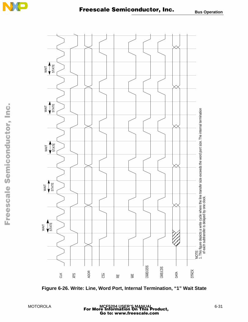
Bus Operation
Fre
esc
ale
Se
mic
on
du
cto
r, I
Freescale Semiconductor, Inc.n
c..
.
Figure 6-26. Write: Line, Word Port, Internal Termination, “1” Wait State
ATS
ADD
R
CSx
RE
WE
DATA
DT A
CK
CLK
UW
E/U
DS
LWE/
LDS
WAI
T
STAT
E
WAI
T
STAT
E
WAI
T
STAT
E
WAI
T
STAT
E
WAI
T
STAT
E
NO
TE:
1. T
his
figur
e de
pict
s a
writ
e cy
cle
whe
re th
e lin
e tra
nsfe
r siz
e ex
ceed
s th
e w
ord
port
size
. The
inte
rnal
term
inat
ion
o
f eac
h su
btra
nsfe
r is
dela
yed
by o
ne c
lock
.
MOTOROLA MCF5204 USER’S MANUAL 6-31 For More Information On This Product,
Go to: www.freescale.com

Bus Operation
Fre
esc
ale
Se
mic
on
du
cto
r, I
Freescale Semiconductor, Inc.n
c..
.
Figure 6-27. IACK: External Termination, “1” Wait State
NOTES:
1. This figure depicts an IACK cycle that is externally terminated at the earliest possible time.
2. IACK cycles are simply read accesses in CPU/IACK space with address bits [4:2] assigned the level of the interrupt and the remaining address bits set to one. Address bits [1:0] are set to zeros.
3. An IACK indication can be generated by configuring a chip-select to “hit” on the IACK address value.
ATS
ADDR
CSx/IACK
RE
WE
DATA[15:8]
DTACK
CLK
UWE/UDS
LWE/LDS
(VECTOR # ADDR[4:2])
WAIT STATE
6-32 MCF5204 USER’S MANUAL MOTOROLA For More Information On This Product,
Go to: www.freescale.com

Bus Operation
Fre
esc
ale
Se
mic
on
du
cto
r, I
Freescale Semiconductor, Inc.n
c..
.
6.8.1 IACK Cycles with Internal Termination
Figure 6-28. IACK: Internal Termination, “0” Wait State
NOTE:
1. This figure depicts an IACK cycle that is internally terminated at the earliest possible time.
ATS
ADDR
CSx/IACK
RE
WE
DATA[15:8]
DTACK
CLK
UWE/UDS
LWE/LDS
(VECTOR # ADDR[4:2])
MOTOROLA MCF5204 USER’S MANUAL 6-33 For More Information On This Product,
Go to: www.freescale.com

Bus Operation
Fre
esc
ale
Se
mic
on
du
cto
r, I
Freescale Semiconductor, Inc.n
c..
.
Figure 6-29. IACK: Internal Termination, “1” Wait State
NOTE:
1. This figure depicts an IACK cycle where the internal termination is delayed by one clock.
ATS
ADDR
CSx/IACK
RE
WE
DATA[15:8]
DTACK
CLK
UWE/UDS
LWE/LDS
(VECTOR # ADDR[4:2])
WAIT STATE
6-34 MCF5204 USER’S MANUAL MOTOROLA For More Information On This Product,
Go to: www.freescale.com
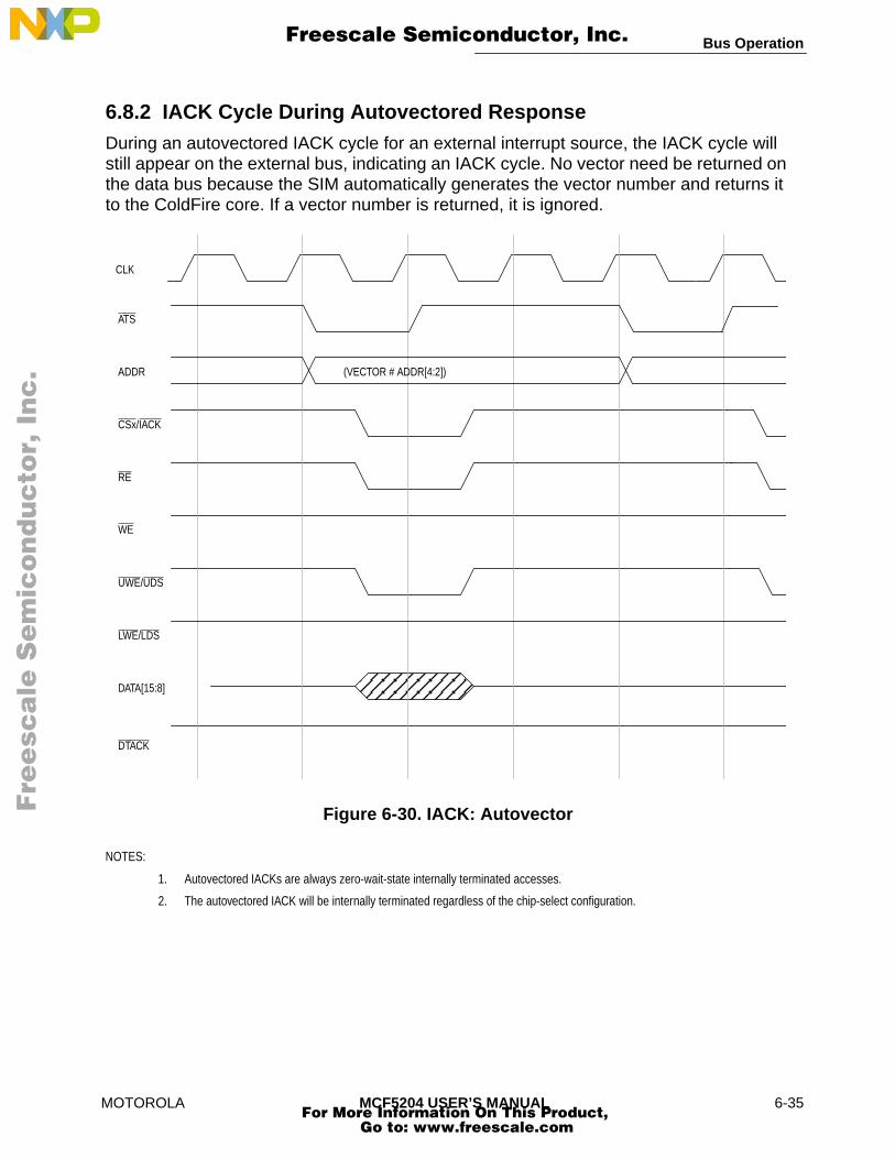
Bus Operation
Fre
esc
ale
Se
mic
on
du
cto
r, I
Freescale Semiconductor, Inc.n
c..
.
6.8.2 IACK Cycle During Autovectored ResponseDuring an autovectored IACK cycle for an external interrupt source, the IACK cycle will still appear on the external bus, indicating an IACK cycle. No vector need be returned on the data bus because the SIM automatically generates the vector number and returns it to the ColdFire core. If a vector number is returned, it is ignored.
Figure 6-30. IACK: Autovector
NOTES:
1. Autovectored IACKs are always zero-wait-state internally terminated accesses.
2. The autovectored IACK will be internally terminated regardless of the chip-select configuration.
ATS
ADDR
CSx/IACK
RE
WE
DATA[15:8]
DTACK
CLK
UWE/UDS
LWE/LDS
(VECTOR # ADDR[4:2])
MOTOROLA MCF5204 USER’S MANUAL 6-35 For More Information On This Product,
Go to: www.freescale.com

Bus Operation
Fre
esc
ale
Se
mic
on
du
cto
r, I
Freescale Semiconductor, Inc.n
c..
.
6.9 RESET OPERATION
Figure 6-31. Reset Operation
6.9.1 ATS ActivationATS is activated by asserting IRQ0 low during the negation of reset. IRQ0 is sampled by the MCF5204 on the rising edge before the negation of RESET. You have 16 full clocks after the negation of RESET to return the IRQ0 input to its inactive state before the ColdFire processor enables the generation of interrupts.
CAUTIONI
To avoid a possible contention problem, you should ensurethat BUSW is not driven after the activation of ATS. ATS isactivated by holding IRQ0 low at the negation of reset. Ifactivation of ATS is preferred, the easiest way to avoidcontention is to drive BUSW with a three-state driver that isenabled with RESET.
6.9.2 BUSW Sample TimeBecause it is a synchronized signal, BUSW should be asserted for at least one clock period. BUSW should be asserted for the two positive clock edges prior to the negation of reset.
CLK
VCC 0V
+5V
BUS
RST
CONTROL
t >= 6CLK CYCLES
t >= 16CLK CYCLES
BUSW/ATS
IRQ0 MODE SELECT INPUT
BUSW/ATSBOOT ROM PORT SIZEINPUT
OUTPUT
6-36 MCF5204 USER’S MANUAL MOTOROLA For More Information On This Product,
Go to: www.freescale.com

DATE: 08-21-98
REVISION NO: 0.1
PAGES AFFECTED: SEE CHANGE BARS
F
ree
sca
le S
em
ico
nd
uc
tor,
I
Freescale Semiconductor, Inc.n
c..
.
SECTION 7SYSTEM INTEGRATION MODULE (SIM)
7.1 SYSTEM INTEGRATION MODULE (SIM) INTRODUCTIONThe System Integration Module (SIM) provides overall control of the internal peripheral devices and the external bus functionality.
The following list summarizes the key SIM features:
• Module Base Address Register (MBAR)
— Base address location of all internal peripherals and SIM resources— Address space masking to internal peripherals and SIM resources
• Interrupt Controller
— Eight individual interrupt sources (four external, four internal)— Programmable interrupt level (1-7) for all interrupts— Programmable priority level (0-3) within each interrupt level
• Programmable Chip-Select Logic
— Six programmable chip-select signals— Programmable wait states and port sizes— Programmable bursting modes— Programmable for internal or external termination— Programmable byte access control signals
• System Protection
— Reset status to indicate cause of last reset— Bus monitor— Spurious Interrupt Monitor— Software Watchdog Timer
• Glueless Bus Interface
• 8-bit General-Purpose I/O Port
MOTOROLA MCF5204 USER’S MANUAL 7-1 For More Information On This Product,
Go to: www.freescale.com

System Integration Module (SIM)
F
ree
sca
le S
em
ico
nd
uc
tor,
I
Freescale Semiconductor, Inc.n
c..
.
7.2 SIM OPERATION
7.2.1 Module Base Address RegisterThe Module Base Address Register (MBAR) determines the base address location of all peripheral modules and SIM registers as well as which access types are allowed for these resources. To access the internal peripherals, customers should write the MBAR with the appropriate base address after system reset.
The MBAR is a 32-bit read/write control register that is accessed in the CPU address space via the MOVEC instruction with an Rc encoding of $C0F. At system reset, the V-bit (valid bit) is cleared and the remainder of the contents of MBAR are uninitialized.
All internal peripheral registers occupy a single memory block that can be located along 1-kbyte boundaries, defined by the base address field in the MBAR. To read or write to these registers customers must set the V-bit of the MBAR, and then the base address field is compared to the upper bits of the logical address to determine if an internal register or peripheral is being accessed. Read accesses to reserved areas in the memory block defined by the MBAR return zeros; write accesses have no effect. Accesses to masked space or addresses outside of the MBAR defined memory region will be external accesses.
7.2.2 Chip-Select OperationThe MCF5204 provides six chip-selects. Internal registers allow the base address, the address range, and functionality of each chip-select to be independently programmed. All address ranges start on 256-byte boundaries and can cover the entire address space. External accesses that do not “hit” in a chip-select range result in a transfer error exception. When internal termination is selected, for a given chip select, wait states can be automatically inserted for zero to seven wait states.
7.2.2.1 PROGRAMMABLE FEATURES.
• Six programmable chip-selects
• Variable block sizes
• Programmed byte-enable modes
• Write-protect capability
• Internal bus cycle termination with programmable wait states
• Full 32-bit address decode with address space checking
7.2.2.2 GLOBAL CHIP-SELECT OPERATION. Global chip-select operation allows address decode for a boot ROM before system initialization. CS0 is the global chip-select whose operation differs from the other external chip-select outputs following reset. When the MCF5204 begins fetching code after reset, CS0 is asserted for every external access until the V-bit is set in the CS0 control register.
7-2 MCF5204 USER’S MANUAL MOTOROLA For More Information On This Product,
Go to: www.freescale.com

System Integration Module (SIM)
F
ree
sca
le S
em
ico
nd
uc
tor,
I
Freescale Semiconductor, Inc.n
c..
.
Global chip-select operation uses internal cycle termination with seven wait states. The BUSW pin at reset determines port size.
Global chip-select does not provide write protection. It responds to all address spaces. While CS0 is in global chip-select mode, no other chip-select (CS5-CS1) can be used. CS0 operates in this manner until the V-bit is set in the CS0 control register, which will then allow the use of CS5-CS1. Customers can program CS0 to continue to decode for a range of addresses after the V-bit is set, provided the desired address range is first loaded into the CS0 base address register. After the V-bit is set for CS0, global chip-select can be restarted only with a system reset.
7.2.2.3 NORMAL CHIP-SELECT OPERATION.
7.2.2.3.1 Chip-Select Prioritization. If overlapping address ranges are programmed into the chip-select registers, only one chip-select will be asserted. Chip-selects are prioritized from CS5 to CS0 with CS5 receiving the highest priority. Note that this chip-select priority is different from previous Motorola products.
7.2.2.3.2 Chip-Select Used for IACK Indication. Dedicated signals to indicate an interrupt acknowledge cycle are not provided; however, customers can program any of the chip-select outputs to provide an IACK indication. This is accomplished by
1. Programming the chip-select mask register to prohibit all accesses except those in CPU/IACK address space, and
2. Programming the chip-select address register with IACK address, FFFF FF 111[4:2]00.
Using a chip-select to provide an IACK indication prevents the use of other addresses within this minimum 512-byte block of addresses inside the CPU/IACK address space.
7.2.3 Bus Timeout Monitor The bus monitor ensures that each external cycle terminates within a reasonable period of time. The bus monitor continuously checks the bus cycle termination response time for external cycles. The bus monitor asserts the internal transfer error, which will result in an access- fault exception if the response time is excessive on external bus cycles. Internal bus cycles always terminate in two cycles.
The BME bit in System Protection Control Register (SYPCR) enables the bus monitor. The bus cycle termination response time is measured in clock cycles with a programmable maximum allowable response time. The BMT bits in the SYPCR determine the bus monitor response timeout period. Customers should choose a value larger than the longest possible response time of the slowest system.
Once the SYPCR is written, the state of the bus timeout monitor cannot be changed as the SYPCR can be written only once.
MOTOROLA MCF5204 USER’S MANUAL 7-3 For More Information On This Product,
Go to: www.freescale.com

System Integration Module (SIM)
F
ree
sca
le S
em
ico
nd
uc
tor,
I
Freescale Semiconductor, Inc.n
c..
.
7.2.4 Spurious Interrupt MonitorWhen an external IACK cycle is not terminated, the bus monitor will time out. The SIM automatically generates the spurious interrupt vector number 24 ($18) to the core processor, which causes the core processor to take a spurious interrupt exception.
7.2.5 Software Watchdog Timer (SWT)The SIM provides the software watchdog timer (SWT) option to prevent system lockup should the software become trapped in loops with no controlled exit. The SWT can be enabled or disabled via the software watchdog enable (SWE) bit in the SYPCR. If enabled, the SWT requires a special service sequence to be executed on a periodic basis. If this periodic servicing action does not occur, the SWT times out and issues a hardware reset or a level 7 interrupt, as programmed by the software watchdog reset/interrupt select bit (SWRI) in the SYPCR. If a reset is generated, the MCF5204 is internally restored to its reset state. Once the software writes the SYPCR, the state of the SWT (enabled or disabled) cannot be changed. The 8-bit interrupt vector for the SWT interrupt is stored in the software watchdog interrupt vector register (SWIVR). The SWP and SWT bits in SYPCR determine the SWT timeout period.
No external reset indication is given in the case of a SWT timeout with hardware reset option. Customers can determine the reset cause by examining the reset status register, RSR.
The SWT service sequence consists of the following two steps: write $55 to SWSR, and write $AA to the SWSR (software watchdog service register). Both writes must occur in the order listed prior to the SWT timeout, but any number of instructions or accesses to the SWSR can be executed between the two writes. This allows any necessary interrupts and exceptions to occur between the two writes.
7-4 MCF5204 USER’S MANUAL MOTOROLA For More Information On This Product,
Go to: www.freescale.com
System Integration Module (SIM)
F
ree
sca
le S
em
ico
nd
uc
tor,
I
Freescale Semiconductor, Inc.n
c..
.
7.2.6 Interrupt ControllerThe SIM provides a centralized interrupt controller for eight interrupt inputs, four external and four internal. The SIM can receive interrupts from external devices and SIM generated interrupts such as the SWT and peripheral modules. External interrupts are driven onto individual interrupt request lines, IRQ[3:0]. Each of the external interrupt sources can have its level and priority defined by programming interrupt control registers in the SIM. Customers can program each interrupt source to autovector to the correct service routine.
NOTE
Any interrupt will flag the processor that an interrupt hasoccurred. It is then up to the processor to check the interruptlines and find out which one was triggered. If the signaldisappears within this time, the processor gets “confused” andruns a spurious interrupt. You should hold the IRQ signal untilthe IACK signal has begun.
For all interrupts, the interrupt level is determined by the Interrupt Control Register (ICR) associated with that interrupt. The priority within each interrupt level for all eight interrupt sources is programmable via the IP1-IP0 bits in the ICRs. As many as four interrupts can be assigned the same interrupt level provided they have unique interrupt priorities. Each interrupt input must have a unique interrupt level and interrupt priority combination. The SIM does not perform any interrupt arbitration cycles. It will decode the highest priority interrupt if multiple interrupt requests occur.
The SIM sends the highest priority, unmasked, pending interrupt request to the core processor. This request can be at level 1 to level 7. The SIM then waits for the core to initiate an interrupt-acknowledge cycle.
Because the timers do not include an interrupt vector register, these modules must always be autovectored. The autovector bits in the ICRs for the timers are hardwired to indicate autovector response. While the SWT cannot be autovectored, it always generates a level-7 interrupt with programmable priority.
All interrupt sources configured for level 7 are edge sensitive. Interrupt sources programmed for levels other than 7 are level sensitive. Interrupt sources must be asserted until the interrupt is acknowledged.
For interrupt sources that are not autovectored, an interrupt-acknowledge output can be generated by dedicating and programming one of the chip-selects to assert for CPU/IACK address space with the correct address range programmed into the chip-select address register. During interrupt processing, the current interrupt service level is driven on address lines A[4:2]. External interrupt sources can compare their priority level with the driven service level and drive their interrupt vector onto the data lines if their priority is higher than the current service level. The external device places the vector number on the
MOTOROLA MCF5204 USER’S MANUAL 7-5 For More Information On This Product,
Go to: www.freescale.com

System Integration Module (SIM)
F
ree
sca
le S
em
ico
nd
uc
tor,
I
Freescale Semiconductor, Inc.n
c..
.
most significant byte of the data signals, DATA[15:8]. In the case of multiple external interrupt sources, the IACK signal can be daisy-chained to indicate the relative priority of the external interrupts.
For autovector responses, the SIM will internally terminate the bus cycle and the SIM will then pass the interrupt vector number to the core processor. An external IACK will appear if a chip-select has been programmed to respond to an IACK cycle. A zero-wait-state read cycle occurs on the external bus during an IACK cycle for an autovectored external interrupt source.
If an internal peripheral module interrupt source is being acknowledged and the AVEC bit in the corresponding ICR is clear, then an internal interrupt-acknowledge cycle occurs. The SIM then passes the interrupt vector number to the core processor.
7.2.7 Reset operationAt power-up, an external POR circuit must assert the MCF5204 RESET pin to reset the device.
7.3 PROGRAMMING MODEL
7.3.1 SIM Registers Memory MapTables 7-1 and 7-2 show the memory map of all the registers in the CPU and SIM. The internal registers in the SIM are memory-mapped registers offset from the SIM Module Base Address pointer, MBAR. MBAR specifies the starting address of the SIM memory map. The MBAR is contained in the CPU memory map.
Note:
• Underlined registers are status or event registers. In these registers, to clear a bit, customers must write a one to that bit location; writing a zero has no effect. Customers should NOT use read-modify-write instructions (such as BSET, BCLR, AND, OR, etc.) with these registers or ALL bits in that register may inadvertently be cleared.
• Addresses not assigned to a register and undefined register bits are reserved for future expansion. Write accesses to these reserved spaces have no effect; read accesses will return zeros.
• If a read access to a write-only register or a write access to a read-only register is attempted, an access fault exception will occur.
7-6 MCF5204 USER’S MANUAL MOTOROLA For More Information On This Product,
Go to: www.freescale.com

System Integration Module (SIM)
F
ree
sca
le S
em
ico
nd
uc
tor,
I
Freescale Semiconductor, Inc.n
c..
.
7.3.2 Memory Map
Table 7-1. CPU Registers Memory Map
ADDRESS NAME WIDTH DESCRIPTION RESET VALUE ACCESS
CPU + $002 CACR 32 Cache Control Register WCPU + $004 ACR0 32 Access Control Register WCPU + $005 ACR1 32 Access Control Register WCPU + $801 VBR 32 Vector Base Register WCPU + $C04 RAMBAR 32 SRAM Base Address Register uninitialized W
CPU + $C0F MBAR 32 Module Base Address Register uninitialized(except V=0) R/W
Table 7-2. SIM Registers Memory Map
ADDRESS NAME WIDTH DESCRIPTION RESET VALUE ACCESS
MBAR + $003 SIMR 8 SIM Configuration Register $C0 R/WMBAR + $004 ReservedMBAR + $014 ICR_E0 8 Interrupt Control Register Ext0 $1C R/WMBAR + $015 ICR_E1 8 Interrupt Control Register Ext1 $04 R/WMBAR + $016 ICR_E2 8 Interrupt Control Register Ext2 $08 R/WMBAR + $017 ICR_E3 8 Interrupt Control Register Ext3 $0C R/WMBAR + $018 8 ReservedMBAR + $019 8 ReservedMBAR + $01A 8 ReservedMBAR + $01B ICR_SW 8 Interrupt Control Register SWT $1F R/WMBAR + $01C ICR_T1 8 Interrupt Control Register T1 $90 R/WMBAR + $01D ICR_T2 8 Interrupt Control Register T2 $94 R/WMBAR + $01E 8 ReservedMBAR + $01F ICR_U1 8 Interrupt Control Register UART1 $18 R/WMBAR + $020 8 ReservedMBAR + $034 IMR 32 Interrupt Mask Register $0000171E R/WMBAR + $038 IPR 32 Interrupt Pending Register $00000000 RMBAR + $03C ReservedMBAR + $040 RSR 8 Reset Status Register $80 or$20 R/WMBAR + $041 SYPCR 8 System Protection Control Register $00 R/WMBAR + $042 SWIVR 8 Software Watchdog Interrupt Vector Register $0F WMBAR + $043 SWSR 8 Software Watchdog Service Register uninitialized WMBAR + $044 Reserved R/WMBAR + $064 CSAR0 32 Chip-Select 0 Base Address Register uninitialized R/WMBAR + $068 CSMR0 32 Chip-Select 0 Address Mask Register uninitialized R/WMBAR + $06C CSCR0 32 Chip-Select 0 Control Register V=0 R/WMBAR + $070 CSAR1 32 Chip-Select 1 Base Address Register uninitialized R/WMBAR + $074 CSMR1 32 Chip-Select 1 Address Mask Register uninitialized R/WMBAR + $078 CSCR1 32 Chip-Select 1 Control Register V=0 R/WMBAR + $07C CSAR2 32 Chip-Select 2 Base Address Register uninitialized R/WMBAR + $080 CSMR2 32 Chip-Select 2 Address Mask Register uninitialized R/WMBAR + $084 CSCR2 32 Chip-Select 2 Control Register V=0 R/WMBAR + $088 CSAR3 32 Chip-Select 3 Base Address Register uninitialized R/WMBAR + $08C CSMR3 32 Chip-Select 3 Address Mask Register uninitialized R/W
MOTOROLA MCF5204 USER’S MANUAL 7-7 For More Information On This Product,
Go to: www.freescale.com

System Integration Module (SIM)
F
ree
sca
le S
em
ico
nd
uc
tor,
I
Freescale Semiconductor, Inc.n
c..
.
7.3.3 SIM Registers7.3.3.1 MODULE BASE ADDRESS REGISTER (MBAR). The MBAR determines the base address location of all internal peripheral modules and SIM resources, and the definition of which types of accesses are allowed for these resources.
The MBAR that follows is a 32-bit control register that physically resides in the SIM. It is accessed in the CPU address space via the MOVEC instruction with an Rc encoding of $C0F. At system reset, the V-bit is cleared and the remainder of the contents of MBAR are uninitialized. To access the internal peripheral modules and SIM resources, MBAR must be written with the appropriate base address after system reset. The V-bit must also be set.
Address space masks are provided as an option for preventing certain types of access (such as user or code access) to modules. A module can place additional address space restrictions on some module registers, regardless of the MBAR address space masks settings.
MBAR + $090 CSCR3 32 Chip-Select 3 Control Register V=0 R/WMBAR + $094 CSAR4 32 Chip-Select 4 Base Address Register uninitialized R/WMBAR + $098 CSMR4 32 Chip-Select 4 Address Mask Register uninitialized R/WMBAR + $09C CSCR4 32 Chip-Select 4 Control Register V=0 R/WMBAR + $0A0 CSAR5 32 Chip-Select 5 Base Address Register uninitialized R/WMBAR + $0A4 CSMR5 32 Chip-Select 5 Address Mask Register uninitialized R/WMBAR + $0A8 CSCR5 32 Chip-Select 5 Control Register V=0 R/WMBAR + $08C ReservedMBAR + $0CB PAR 8 Pin Assignment Register $00 R/WMBAR + $1C5 PADDR 8 Port A Data Direction Register $00 R/WMBAR + $1C9 PADAT 8 Port A Data Register uninitialized R/W
Table 7-2. SIM Registers Memory Map (Continued)
ADDRESS NAME WIDTH DESCRIPTION RESET VALUE ACCESS
BA31 BA30 BA29 BA28 BA27 BA26 BA25 BA24 BA23 BA22 BA21 BA20 BA19 BA18 BA17 BA16
31 30 29 28 27 26 25 24 23 22 21 20 19 18 17 16
- - - - - - - - - - - - - - - -RESET:
BA15 BA14 BA13 BA12 BA11 BA10 BA9 RSVD RSVD RSVDI C/I SC SD UC UD V
15 14 13 12 11 10 9 8 7 6 5 4 3 2 1 0
- - - - - - - - - - - - - - - 0RESET:
Read/Write
CPU+$C0FMBAR
7-8 MCF5204 USER’S MANUAL MOTOROLA For More Information On This Product,
Go to: www.freescale.com

System Integration Module (SIM)
F
ree
sca
le S
em
ico
nd
uc
tor,
I
Freescale Semiconductor, Inc.n
c..
.
7.3.3.1.1 BA31-BA9- Base Address. This field defines the base address location of all peripheral modules and SIM resources.
7.3.3.1.2 C/I,SC,SD,UC,UD - Address Space Masks.
• C/I - Mask CPU/IACK space in address range
• SC - Mask supervisor code space in address range
• SD - Mask supervisor data space in address range
• UC - Mask user code space in address range
• UD - Mask user data space in address range
— Mask Bit = 0; Accesses are allowed in this address range— Mask Bit = 1; Accesses are not allowed in this address range
7.3.3.1.3 V - Valid. This bit indicates when the contents of the MBAR are valid. Until the V-bit is set, the base address value is not used, and all peripheral modules and SIM resources are not accessible. An external bus cycle is generated if the base address field matches the logical address and the V bit is clear.
0 = Contents of MBAR are not valid1 = Contents of MBAR are valid
7.3.3.2 SIM CONFIGURATION REGISTER (SIMR). The SIMR controls the operation of SWT and bus timeout monitor when the CPU is halted or during the assertion of soft reset.
The SIMR is an 8-bit read/write register. At system reset, bits FRZ1 and FRZ0 are set.
7.3.3.2.1 FRZ1 - Freeze Software Watchdog Timer Enable.
0 = When CPU is halted, the software watchdog timer continues to run1 = When CPU is halted, the software watchdog timer is disabled
7.3.3.2.2 FRZ0 - Freeze Bus Monitor Enable.
0 = When CPU is halted, the bus monitor continues to run1 = When CPU is halted, the bus monitor is disabled
FRZ1 FRZ0
7 6 5 4 3 2 1 0
1 1 0 0 0 0 0 0RESET:
Reserved
$003
Read/Write
SIMR
MOTOROLA MCF5204 USER’S MANUAL 7-9 For More Information On This Product,
Go to: www.freescale.com

System Integration Module (SIM)
F
ree
sca
le S
em
ico
nd
uc
tor,
I
Freescale Semiconductor, Inc.n
c..
.
7.3.3.3 INTERRUPT CONTROL REGISTER (ICR_XX). The ICR contains the interrupt and priority levels assigned to each interrupt input. There will be one ICR for each interrupt input. There are eight interrupt inputs: four external inputs, the SWT interrupt generated within the SIM, and three peripheral module interrupts. The peripheral module interrupts consist of the two timer channels and the UART. Each ICR must have a unique interrupt level and interrupt priority combination.
The ICRs are 8-bit read/write registers. At system reset, each ICR is initialized to a unique value.
7.3.3.3.1 AVEC - Autovector Enable. This bit determines if the interrupt-acknowledge cycle for the interrupt level indicated in IL2-IL0 for each interrupt input requires an autovector response. If this bit is set, the SIM will internally generate the vector number, which is the sum of the interrupt level, IL2-IL0, plus 24. There are seven distinct autovectors that can be used corresponding to the seven interrupt levels. If this bit is cleared, the external device or peripheral module must return the vector number during an external or peripheral interrupt acknowledge cycle.
NOTE
The SWT must not be autovectored. Customers must makecertain the autovector bit in the SWT ICR is programmed to 0.
0 = Interrupting source returns vector number during interrupt-acknowledge cycle
1 = SIM internally generates vector number during interrupt-acknowledge cycle
7.3.3.3.2 IL2-IL0 - Interrupt Level. These bits indicate the interrupt level assigned to each external and peripheral module interrupt input. Level 7 is the highest priority; level 1 is the lowest; and level 0 indicates that no interrupt is requested. If the SWT is programmed to issue an interrupt, its corresponding IL2-IL0 are hardwired to indicate a level-7 interrupt. Similarly, the AVEC bits in the ICRs for the timers are hardwired to a value of 1 because the timers cannot return an interrupt vector. The ICRs can have similar interrupt levels; however, if these have nonunique priorities within, indeterminate results may occur.
7.3.3.3.3 IP1-IP0 - Interrupt Priority. These bits indicate the priority within an interrupt level assigned to each SIM interrupt input. As many as four interrupts can be assigned the
AVEC - - IL2 IL1 IL0 IP1 IP0
7 6 5 4 3 2 1 0
0 0 0 0 0 0 0 0RESET:
$014, $015, $016, $017, $01B, $01C, $01D, $01F
Read/Write
SIMR
7-10 MCF5204 USER’S MANUAL MOTOROLA For More Information On This Product,
Go to: www.freescale.com

System Integration Module (SIM)
F
ree
sca
le S
em
ico
nd
uc
tor,
I
Freescale Semiconductor, Inc.n
c..
.
same interrupt level provided they have unique interrupt priorities. IP1-IP0 = 3 is the highest priority, and IP1-IP0 = 0 is the lowest priority for a given interrupt level. If the ICRs are programmed to have nonunique interrupt levels and priority combinations, indeterminate results will occur.
There are eight ICR registers in the SIM. Refer to Table 7-2 for register assignments and reset values.
7.3.3.4 INTERRUPT MASK REGISTER (IMR). Each bit in the IMR corresponds to an interrupt source. The customer masks an interrupt by setting the corresponding bit in the IMR and enables an interrupt by clearing the corresponding bit in the IMR. When a masked interrupt occurs, the corresponding bit in the Interrupt Pending Register (IPR) is set, regardless of the IMR bit, but no interrupt request is passed along to the core processor.
The IMR is a 32-bit read/write register. At system reset, all mask bits are initialized to logic one, masking all interrupt sources.
7.3.3.4.1 IMK - Interrupt Mask.
0 = Enable interrupt request1 = Mask interrupt request
Note: IRQ0 corresponds to ICR_E0 IRQ1 corresponds to ICR_E1IRQ2 corresponds to ICR_E2IRQ3 corresponds to ICR_E3SWT corresponds to ICR_SW T1 corresponds to ICR_T1T2 corresponds to ICR_T2UART1 corresponds to ICR_U1
- - - - - - - - - - - - - - - -
31 30 29 28 27 26 25 24 23 22 21 20 19 18 17 16
0 0 0 0 0 0 0 0 0 0 0 0 0 0 0 0RESET:
- - - UART - T2 T1 SWT - - - IRQ3 IRQ2 IRQ1 IRQ0 -
15 14 13 12 11 10 9 8 7 6 5 4 3 2 1 0
0 0 0 1 0 1 1 1 0 0 0 1 1 1 1 0RESET:
$034
Read/Write
IMR
MOTOROLA MCF5204 USER’S MANUAL 7-11 For More Information On This Product,
Go to: www.freescale.com

System Integration Module (SIM)
F
ree
sca
le S
em
ico
nd
uc
tor,
I
Freescale Semiconductor, Inc.n
c..
.
7.3.3.5 INTERRUPT PENDING REGISTER (IPR). Each labeled bit in the IPR corresponds to a SIM interrupt source. When the SIM receives an interrupt, the SIM interrupt controller sets the corresponding bit in the IPR. An active interrupt request appears as a set bit in the IPR. It is the responsibility of the interrupting source to clear its interrupt request after the interrupt-acknowledge cycle.
The IPR is a 32-bit read-only register. At system reset, all bits are initialized to zero.
7.3.3.5.1 IPN - Interrupt Pending.
0 = No interrupt request1 = Interrupt asserted
Note: IRQ0 corresponds to ICR_E0IRQ1 corresponds to ICR_E1IRQ2 corresponds to ICR_E2IRQ3 corresponds to ICR_E3SWT corresponds to ICR_SWT1 corresponds to ICR_T1T2 corresponds to ICR_T2UART1 corresponds to ICR_U1
- - - - - - - - - - - - - - - -
31 30 29 28 27 26 25 24 23 22 21 20 19 18 17 16
0 0 0 0 0 0 0 0 0 0 0 0 0 0 0 0RESET:
- - - UART - T2 T1 SWT IRQ3 IRQ2 IRQ1 IRQ0 -
15 14 13 12 11 10 9 8 7 6 5 4 3 2 1 0
0 0 0 0 0 0 0 0 0 0 0 0 0 0 0- 0RESET:
$038
Read Only
IPR
7-12 MCF5204 USER’S MANUAL MOTOROLA For More Information On This Product,
Go to: www.freescale.com

System Integration Module (SIM)
F
ree
sca
le S
em
ico
nd
uc
tor,
I
Freescale Semiconductor, Inc.n
c..
.
7.3.3.6 RESET STATUS REGISTER (RSR). The RSR contains a bit for each reset source to the SIM. A set bit indicates the last type of reset that occurred. The RSR is updated by the reset control logic when the reset is complete. Customers should clear this register after every reset so the register will reflect the cause of the most recent reset. A bit is cleared by writing a one to that bit location; writing a zero has no effect.
The RSR is an 8-bit read/write register. At system reset, the RSR fields HRST and SWTR are initialized to 1 and 0, respectively.
7.3.3.6.1 HRST - Hard Reset or System Reset. 1 = The last reset was caused by an external device driving RESET. Assertion of hard reset (RESET) by an external device causes the core processor to take a reset exception. All registers including configuration registers in the core, peripherals, and SIM modules are reset.
7.3.3.6.2 SWTR - Software Watchdog Timer Reset. 1 = The last reset was caused by the software watchdog timer. If SWRI bit in the System Protection Control Register (SYPCR) is set, and the software watchdog timer times out, a hard reset occurs.
7.3.3.7 SYSTEM PROTECTION CONTROL REGISTER (SYPCR). The SYPCR controls the software watchdog timer, bus monitor enables, and timeout functionality.
The SYPCR is an 8-bit read/write register. The register may be read at anytime but can be written only once after system reset. Subsequent writes to the SYPCR will have no effect. At system reset, the software watchdog timer is disabled; the bus monitor is disabled and initialized with the maximum timeout period.
7.3.3.7.1 SWE - Software Watchdog Enable. This control bit enables the software watchdog.
0 = SWT is disabled1 = SWT is enabled
HRST - SWTR - - - - -
7 6 5 4 3 2 1 0
1 0 0 0 0 0 0 0RESET:
$040
Read/Write
RSR
SWE SWRI SWP SWT1 SWT0 BME BMT1 BMT0
7 6 5 4 3 2 1 0
0 0 0 0 0 0 0 0RESET:
$041
Read/Write
SYPCR
MOTOROLA MCF5204 USER’S MANUAL 7-13 For More Information On This Product,
Go to: www.freescale.com

System Integration Module (SIM)
F
ree
sca
le S
em
ico
nd
uc
tor,
I
Freescale Semiconductor, Inc.n
c..
.
7.3.3.7.2 SWRI - Software Watchdog Reset/Interrupt Select. This control bit selects the action taken by the software watchdog timer at timeout.
0 = SWT causes a level 7 interrupt to the core processor1 = SWT causes a hardware reset
7.3.3.7.3 SWP - Software Watchdog Prescaler. This control bit enables the prescalar for the software watchdog.
0 = SWT clock is not prescaled1 = SWT clock is prescaled by a value of 512
7.3.3.7.4 SWT1-SWT0 - Software Watchdog Timing. These bits, along with the SWP bit, select the timeout period for the SWT as shown in Table 7-3.
Note
When the SWP and SWT bits are modified to select a newsoftware timeout, the software service sequence ($55followed by $AA written to the SWSR) must be performedbefore the new timeout period takes effect.
7.3.3.7.5 BME - Bus Monitor External Enable. This control bit enables the bus monitor.
0 = Disable bus monitor function for external cycles only1 = Enable bus monitor function for external cycles
Table 7-3. SWT Timeout
SWP SWT[1:0] SWT TIME-OUT PERIOD
0 00 29 system clocks
0 01 211 system clocks
0 10 213 system clocks
0 11 215system clocks
1 00 218 system clocks
1 01 220 system clocks
1 10 222 system clocks
1 11 224 system clocks
7-14 MCF5204 USER’S MANUAL MOTOROLA For More Information On This Product,
Go to: www.freescale.com

System Integration Module (SIM)
F
ree
sca
le S
em
ico
nd
uc
tor,
I
Freescale Semiconductor, Inc.n
c..
.
7.3.3.7.6 BMT1-BMT0 - Bus Monitor Timing. These bits select the timeout period for the bus monitor as shown in Table 7-4. After system reset, the bus monitor is set to timeout after 1024 system clocks.
7.3.3.8 SOFTWARE WATCHDOG INTERRUPT VECTOR REGISTER (SWIVR). The SWIVR contains the 8-bit interrupt vector that the SIM returns during an interrupt- acknowledge cycle in response to an interrupt the SWT generates.
The SWIVR is an 8-bit register, which is set to the uninitialized vector $0F at system reset.
Do not autovector the SWT.
7.3.3.9 SOFTWARE WATCHDOG SERVICE REGISTER (SWSR). The SWSR is the location to which the SWT servicing sequence is written. To prevent an SWT timeout, customers should write a $55 followed by a $AA to this register.
The SWSR is an 8-bit register. At system reset, the contents of SWSR are uninitialized.
Table 7-4. BMT Timeout
BMT1 - BMT0 BUS MONITOR TIME-OUT PERIOD
00 1024 system clocks
01 512 system clocks
10 256 system clocks
11 128 system clocks
SWIV7 SWIV6 SWIV5 SWIV4 SWIV3 SWIV2 SWIV1 SWIV0
7 6 5 4 3 2 1 0
0 0 0 0 1 1 1 1RESET:
$042
Write Only
SWIVR
SWSR7 SWSR6 SWSR5 SWSR4 SWSR3 SWSR2 SWSR1 SWSR0
- - - - - RESET:
$043
Write Only
SWSR
- - -
7 6 5 4 3 2 1 0
MOTOROLA MCF5204 USER’S MANUAL 7-15 For More Information On This Product,
Go to: www.freescale.com

System Integration Module (SIM)
F
ree
sca
le S
em
ico
nd
uc
tor,
I
Freescale Semiconductor, Inc.n
c..
.
7.3.4 Chip-Select Registers7.3.4.1 CHIP-SELECT BASE ADDRESS REGISTER (CSARX). The following paragraphs describe the registers in the chip-select function. The chip-select registers cannot be used until the V-bit is set in the Chip-Select Control Register (CSCRX). There are six 32-bit base address registers in the chip-select function, one for each chip-select signal.
If overlapping address ranges are programmed into the chip-select registers, only one chip-select will be asserted. Chip-selects are prioritized from CS5 to CS0 with CS5 receiving the highest priority. Please note this is different from previous Motorola products.
7.3.4.1.1 BA21-BA8: Base Address Bits [21:8]. The base address field selects the starting address for the chip-select. The base address field is compared to the internal core address to determine whether a chip-select should be generated.
There are six chip-select base address registers. Refer to Table 7-2 for assignments and reset values.
BA31 BA30 BA29 BA28 BA27 BA26 BA25 BA24 BA23 BA22 BA21 BA20 BA19 BA18 BA17 BA16
31 30 29 28 27 26 25 24 23 22 21 20 19 18 17 16
0 0 0 0 0 0 0 0 0 0 0 0 0 0 0 0
BA15 BA14 BA13 BA12 BA11 BA10 BA9 - - - - - - - - -
15 14 13 12 11 10 9 8 7 6 5 4 3 2 1 0
0 0 0 0 0 0 0 - - - - - - - - -RESET:
$064, $070, $07C, $088, $094, $0A0
Read/Write
CSARX
RESET:
7-16 MCF5204 USER’S MANUAL MOTOROLA For More Information On This Product,
Go to: www.freescale.com

System Integration Module (SIM)
F
ree
sca
le S
em
ico
nd
uc
tor,
I
Freescale Semiconductor, Inc.n
c..
.
7.3.4.2 CHIP-SELECT ADDRESS MASK REGISTER (CSMRX).
7.3.4.2.1 BAM31-BAM9: Address Mask Bits[31:9]. The address mask field—the upper 23 bits of each address mask register—defines the chip-select block size. The block size equals 2 ** n (where n is the number of bits set in the address mask field + 9). Any set bit masks the corresponding base address register bit (the base address register bit becomes a “don’t care”). By masking the address bits independently, external devices of different size address ranges can be used. Address mask bits can be set or cleared in any order in the field. This allows a resource to reside in more than one area of the address map. This field can be read or written at any time.
BAMn = 0; Corresponding address bit is used in chip-select decodeBAMn = 1; Corresponding address bit is ignored in chip-select decode
7.3.4.2.2 WP: Write Protect. This bit can restrict write accesses to the address range in a base address register. An access fault exception will be taken for any attempt to write to the range of addresses specified in a base address register that has this bit set.
1 = Only read accesses are allowed0 = Either read or write accesses are allowed
7.3.4.2.3 C/I,SC,SD,UC,UD - Address Space Masks.
• C/I - Mask CPU/IACK space in address range
• SC - Mask supervisor code space in address range
• SD - Mask supervisor data space in address range
• UC - Mask user code space in address range
• UD - Mask user data space in address range
— Mask Bit = 0; accesses are allowed in address range— Mask Bit = 1; accesses are ignored in address range
There are six chip-select mask registers. Refer to Table 7-2 for assignments and reset values.
BAM31 BAM30 BAM29 BAM28 BAM27 BAM26 BAM25 BAM24 BAM23 BAM22 BAM21 BAM20 BAM19 BAM18 BAM17 AM16
31 30 29 28 27 26 25 24 23 22 21 20 19 18 17 16
0 0 0 0 0 0 0 0 0 0 0 0 0 0 0 0RESET:
BAM15 BAM14 BAM13 BAM12 BAM11 BAM10 BAM9 WP RSVD RSVD C/I SC SD UC UD -
15 14 13 12 11 10 9 8 7 6 5 4 3 2 1 0
0 0 0 0 0 0 0 0 0 0 0 0 0 0 0 -RESET:
$068, $074, $080, $08C, $098, $0A4
Read/Write
CSMRX
MOTOROLA MCF5204 USER’S MANUAL 7-17 For More Information On This Product,
Go to: www.freescale.com

System Integration Module (SIM)
F
ree
sca
le S
em
ico
nd
uc
tor,
I
Freescale Semiconductor, Inc.n
c..
.
7.3.5 Chip-Select Control Register(CSCRx)
7.3.5.1 WS[2:0]- WAIT STATES. This field is valid when AA = 1 and defines the number of wait states that will be inserted before an internal transfer-acknowledge is generated. If an external transfer-acknowledge is received before the indicated number of wait states is generated, the external transfer acknowledge will terminate the cycle.
7.3.5.2 AA - AUTO ACKNOWLEDGE ENABLE. This bit controls the assertion of the internal transfer-acknowledge.
0 = Wait for external transfer-acknowledge1 = Wait for internal transfer-acknowledge specified by WS[2:0]
7.3.5.3 PS: PORT SIZE. This bit determines the port size associated with a given chip-select. If this bit is set, then the port size is a byte. If this bit is reset to zero, then the port size is a word (16 bits).
1 = 8 - bit port size - Data sampled and driven on D[15:8]0 = 16 - bit port size - Data sampled and driven on D[15:0]
7.3.5.4 BRST - BURST ENABLE. This bit specifies the burst capability of the memory associated with each chip-select. If this bit is set, all read accesses from a port size
Table 7-5. Wait State Encoding
WS2 WS1 WS0 RESPONSE
0 0 0 Zero Wait States
0 0 1 One Wait State
1 1 0 Six Wait States
1 1 1 Seven Wait States
- - - - - - - - - - - - - - -
31 30 29 28 27 26 25 24 23 22 21 20 19 18 17 16
- - - - - - - - - - - - - - - -RESET:
- - - WS2 WS1 WS0 BRST AA - PS BEM - - - - V
15 14 13 12 11 10 9 8 7 6 5 4 3 2 1 0
- - - 0 0 0 0 0 - 0 0 - - - - 0RESET:
-
$06C, $078, $084, $090, $09C, $0A8
Read/Write
CSCRX
7-18 MCF5204 USER’S MANUAL MOTOROLA For More Information On This Product,
Go to: www.freescale.com

System Integration Module (SIM)
F
ree
sca
le S
em
ico
nd
uc
tor,
I
Freescale Semiconductor, Inc.n
c..
.
smaller than the requested transfer size will be bursted— including longword transfers to 8/16 - bit ports, word transfer to 8 - bit ports, and line transfers to 8/16/32 - bit ports.
0 = Burst transfer not allowed1 = Burst transfer allowed
When set to logic 1, accesses to this chip-select address space are enabled to burst. Bursting can occur on any access where the size of the memory operand is greater than the port size (e.g. LW to W, W to B, any line sized access). Bursting access will occur only on read access, with internal termination, with the burst-enable bit set. The bursting mode supports programmable wait states.
Bursted access does not negate the chip-select or read-enable between subtransfers. Only the address field changes. Bursted accesses with wait states greater than zero complete faster than normal access, allowing for increased performance, especially with respect to cache line fills. See Section 6 Bus Operations for an example of bursted access.
7.3.5.5 BEM: BYTE MODE ENABLE. The MCF5204 offers two modes of functionality for byte enables. The default mode is designed for SRAM, ROM, and FLASH parts that have the standard CE, WE, and OE pins. All chip-selects use this default mode after reset. Certain SRAMS have byte enables that must be asserted during reads (in addition to writes). To accommodate these SRAMS, another mode of byte enable can be invoked by setting the BEM bit in the relevant chip-select address register.
The two modes of byte-enable functionality are shown in Table 7-6. The signal names below refer to the UWE and LWE pins. All signals in all modes have the same timing as the byte enables shown in Section 6 Bus Operations.
7.3.5.6 V: VALID BIT. This bit indicates that the contents of its Base Address Register, Address Mask Register, and Chip-Select Control Registers are valid. The programmed chip-selects do not assert until the V-bit is set. A reset clears the V-bit in each Chip-Select Control Register and clears the mask bits in the Chip-Select Address Register. All other bits are unaffected by reset. (CS[0] is a special case. See subsection 7.2.2.2 on Global Chip-Select Operation ).
Table 7-6. Byte Enable Mode
PIN NAME BEM = 0 BEM = 1
UWE Upper Write Enable Asserted low during writes to data[15:8]
Upper Data StrobeAsserted low during both read and write to data[15:8]
LWE Lower Write Enable Asserted low during writes to data[7:0]
Lower Data StrobeAsserted low during both read and write to data[7:0]
MOTOROLA MCF5204 USER’S MANUAL 7-19 For More Information On This Product,
Go to: www.freescale.com

System Integration Module (SIM)
Fre
esc
ale
Se
mic
on
du
cto
r, I
Freescale Semiconductor, Inc.n
c..
.
V - ValidThis bit defines when the chip-select is valid.
0 = Chip-select invalid1 = Chip-select valid
There are six Chip-Select Control Registers. Refer to Table 7-2 for assignments and reset values.
7.4 GENERAL-PURPOSE I/O PORT (PORT A) CONFIGURATION REGISTERS
The general-purpose I/O pins are muxed with the UART module pins, timer module pins, and two address pins. These pins can be selected as general-purpose I/O pins even when other pins related to the same on-chip peripheral are used as dedicated pins. If an input pin to an I/O peripheral is used as a general-purpose I/O pin, the actual input to the peripheral is automatically connected internally to VDD or GND based on the pin's function. This does not affect the operation of the port I/O pins in their general-purpose I/O function. Even if all the module pins for a particular peripheral are configured as general-purpose I/O, the peripheral can still operate, though without external stimulus.
7.4.1 Pin Assignment Register (PAR)The PAR lets customers select certain signal pin assignments. The parallel port is multiplexed onto various pins including A21, A20, timer, and UART pins.
Each pin can be independently configured to operate as its original device function or as a parallel port bit. Table 7-7 displays the pin functionality when PARx bits are set to 0 or 1.
Table 7-7. PAR Pin Assignment
PARX 0 1
PAR0 A20 PA0
PAR1 A21 PA1
PAR2 TIN PA2
PAR3 TOUT PA3
PAR7 PAR6 PAR5 PAR4 PAR3 PAR2 PAR1 PAR0
7 6 5 4 3 2 1 0
0 0 0 0 0 0 0 0RESET:
$CB
Read/Write
PAR
7-20 MCF5204 USER’S MANUAL MOTOROLA For More Information On This Product,
Go to: www.freescale.com

System Integration Module (SIM)
Fre
esc
ale
Se
mic
on
du
cto
r, I
Freescale Semiconductor, Inc.n
c..
.
7.4.1.1 PORT A DATA DIRECTION REGISTER (PADDR). For each port pin, when acting as a general-purpose I/O pin, the signal direction for that pin is determined by the corresponding control bit in the Port A Data Direction Register (PADDR). The port I/O pin is configured as an input if the corresponding PADDR bit is cleared; it is configured as an output if the corresponding PADDR bit is set. All PADDR and PAR bits are cleared on cold reset, configuring all Port A pins as the on-chip peripheral pins.
Logic 0 - Parallel port is input Logic 1 - Parallel port is output
7.4.1.2 PORT A DATA REGISTER (PADAT). When a port pin is used as general-purpose I/O, it may be accessed through the Port A Data Register (PADAT). Data written to the PADAT is stored in an output latch.
If a port pin is configured as an output, the output latch data is gated onto the port pin. In this case, when the PADAT is read, the contents of the output latch data associated with the output port pin is read.
PAR4 TXD PA4
PAR5 RXD PA5
PAR6 CTS PA6
PAR7 RTS PA7
Table 7-7. PAR Pin Assignment (Continued)
PARX 0 1
PADDR7 PADDR6 PADDR5 PADDR4 PADDR3 PADDR2 PADDR1 PADDR0
RESET:
Read/Write
PADDR $1C5
7 6 5 4 3 2 1 0
0 0 0 0 0 0 0 0
PADAT7 PADAT6 PADAT5 PADAT4 PADAT3 PADAT2 PADAT1 PADAT0
- - - - - - - -RESET:
Read/Write
PADAT $1C9
7 6 5 4 3 2 1 0
MOTOROLA MCF5204 USER’S MANUAL 7-21 For More Information On This Product,
Go to: www.freescale.com

System Integration Module (SIM)
Fre
esc
ale
Se
mic
on
du
cto
r, I
Freescale Semiconductor, Inc.n
c..
.
If a port pin is configured as an input, data written to PADAT is still stored in the output latch but is prevented from reaching the port pin. In this case, when PADAT is read, the current state of the port pin is read.
The processor can write to the PADAT register at anytime. If the port pin is configured as input, the processor can read the pin's value without corrupting the PADAT register. If the port bit is subsequently switched to be output, the previously written value of PADAT will be driven on the pin.
7-22 MCF5204 USER’S MANUAL MOTOROLA For More Information On This Product,
Go to: www.freescale.com

DATE: 08-21-98
REVISION NO: 0.1
PAGES AFFECTED: SEE CHANGE BARS
F
ree
sca
le S
em
ico
nd
uc
tor,
I
Freescale Semiconductor, Inc.n
c..
.
SECTION 8UART MODULE
The MCF5204 contains one universal asynchronous/synchronous receiver/transmitter (UART). The UART is clocked by the system clock, which eliminates the need for an external crystal.
The UART module, shown in Figure 8-1, consists of the following major functional areas:
• Serial Communication Channel
• 16-Bit Timer for Baud-Rate Generation
• Internal Channel Control Logic
• Interrupt Control Logic
Figure 8-1. UART Block Diagram
SERIAL COMMUNICATION
CHANNEL
16-BIT TIMER
FOR BAUD RATE GENERATION
INTERNAL CHANNEL
CONTROL LOGIC
INTERRUPT CONTROL
LOGIC
CTS
RTS
RXD
TXD
SYSTEM CLOCK
TIN (EXTCLK)
MOTOROLA MCF5204 USER’S MANUAL 8-1 For More Information On This Product,
Go to: www.freescale.com

UART Module
F
ree
sca
le S
em
ico
nd
uc
tor,
I
Freescale Semiconductor, Inc.n
c..
.
8.1 MODULE OVERVIEWThe MCF5204 contains one independent UART module. Features of the UART module include the following:
• UART Clocked by the System Clock or External Clock (TIN)
• Full Duplex Asynchronous/synchronous Receiver/transmitter Channel
• Quadruple-Buffered Receiver
• Double-Buffered Transmitter
• Independently Programmable Baud Rate for Receiver and Transmitter Selectable from:— Timer-generated baud rate or external clock
• Programmable Data Format:
— Five to eight data bits plus parity— Odd, even, no parity, or force parity— .563 to 2 stop bits in x16 mode(asynchronous)/1or 2 stop bits in synchronous
mode
• Programmable Channel Modes:
— Normal (full duplex)— Automatic echo— Local loopback— Remote loopback
• Automatic Wakeup Mode for Multidrop Applications
• Four Maskable Interrupt Conditions
• Parity, Framing, Break, and Overrun Error Detection
• False Start Bit Detection
• Line-Break Detection and Generation
• Detection of Breaks Originating in the Middle of a Character
• Start/End Break Interrupt/status
8.1.1 Serial Communication Channel The communication channel provides a full duplex asynchronous/synchronous receiver and transmitter using an operating frequency derived from the system clock or from an external clock tied to the TIN pin.
The transmitter accepts parallel data from the CPU; converts it to a serial bit stream; inserts the appropriate start, stop, and optional parity bits; then outputs a composite serial data stream on the channel transmitter serial data output (TxD). Refer to subsection 8.3.2.1 Transmitter for additional information.
8-2 MCF5204 USER’S MANUAL MOTOROLA For More Information On This Product,
Go to: www.freescale.com
UART Module
F
ree
sca
le S
em
ico
nd
uc
tor,
I
Freescale Semiconductor, Inc.n
c..
.
The receiver accepts serial data on the channel receiver serial data input (RxD); converts it to parallel format; checks for a start bit, stop bit, parity (if any), or any error condition; and transfers the assembled character onto the bus during read operations. The receiver can be polled or interrupt driven. Refer to subsection 8.3.2.2 Receiver for additional information.
8.1.2 Baud-Rate Generator/TimerThe 16-bit UART timer, clocked by the system clock, can function as an asynchronous x16 clock. In addition, you can tie an external clock to the TIN pin of the MCF5204 timer for use as a synchronous or asynchronous clocking source for the UART.
8.1.3 Interrupt Control Logic An internal interrupt request signal (IRQ) notifies the MCF5204 interrupt controller of an interrupt condition. The output is the logical NOR of all (as many as four) unmasked interrupt status bits in the UART Interrupt Status Register (UISR). You program the UART Interrupt Mask Register (UIMR) to determine which interrupts will be valid in the UISR.
The UART module interrupt level is programmed in the MCF5204 interrupt controller external to the UART module. You can configure the UART to supply the vector from the UART Interrupt Vector Register (UIVR) or program the SIM to provide an autovector when a UART interrupt is acknowledged.
You can also program the interrupt level, priority within the level, and autovectoring capability in the SIM register ICR_U1.
8.2 UART MODULE SIGNAL DEFINITIONSThe following paragraphs contain a brief description of the UART module signals. Figure 8-2 shows both the external and internal signal groups.
NOTE
The terms assertion and negation are used throughout thissection to avoid confusion when dealing with a mixture ofactive-low and active-high signals. The term assert orassertion indicates that a signal is active or true, independentof the level represented by a high or low voltage. The termnegate or negation indicates that a signal is inactive or false.
8.2.1 Transmitter Serial Data Output (TxD) This signal is the transmitter serial data output. The output is held high ('‘mark’' condition) when the transmitter is disabled, idle, or operating in the local loopback mode. Data is shifted out on this signal on the falling edge of the clock source, with the least significant bit transmitted first. All UART pins are muxed with the parallel port. Their functionality is determined by programming the Pin Assignment Register (PAR) in the SIM.
MOTOROLA MCF5204 USER’S MANUAL 8-3 For More Information On This Product,
Go to: www.freescale.com

UART Module
F
ree
sca
le S
em
ico
nd
uc
tor,
I
Freescale Semiconductor, Inc.n
c..
.
8.2.2 Receiver Serial Data Input (RxD) This signal is the receiver serial data input. Data received on this signal is sampled on the rising edge of the clock source, with the least significant bit received first.
8.2.3 Request-To-Send (RTS ) You can program this active-low output signal to be automatically negated and asserted by either the receiver or transmitter. When connected to the clear-to-send (CTS) input of a transmitter, this signal controls serial data flow.
8.2.4 Clear-To-Send (CTS ) This active-low input is the clear-to-send input and can generate an interrupt on change-of-state.
Figure 8-2. External and Internal Interface Signals
INTERNAL
CONTROL
LOGIC
FOUR-CHARACTERRECEIVE BUFFER
TWO-CHARACTERTRANSMIT BUFFER
INPUT PORT
OUTPUT PORT
EXTE
RN
AL IN
TER
FAC
E SI
GN
ALS
INTE
RFA
CE
TO C
PU
UAR
T M
OD
ULE
INTE
RN
AL B
US
ADDRESS BUS
CONTROL
DATA
16-BIT TIMER/BAUD RATE GENERATOR
SYSTEM CLOCK
IRQ
CTS
RTS
RXD
TXD
TIN(EXTCLK)
8-4 MCF5204 USER’S MANUAL MOTOROLA For More Information On This Product,
Go to: www.freescale.com

UART Module
F
ree
sca
le S
em
ico
nd
uc
tor,
I
Freescale Semiconductor, Inc.n
c..
.
8.3 OPERATION The following paragraphs describe the operation of the baud-rate generator, transmitter and receiver, and other operating modes of the UART module.
8.3.1 Baud-Rate Generator/TimerYou must note that the timer references made here relative to clocking the UART are different than the MCF5204 timer module that is integrated on the bus of the ColdFire core. The UART has a baud generator based on an internal timer that is dedicated to the UART. You can program the Clock Select Register(USCR) to enable this timer or an external clock source from TIN to generate baud rates. When the internal timer is used, a prescaler supplies an asynchronous 16x clock source to the timer. The timer register value is programmed with the UBG1 and UBG2 registers. See subsections 8.4.1.12 and 8.4.1.13 for more information.
An external TIN clock source, when enabled in the USCR, can generate an x1 or x16 asynchronous or synchronous clock to the UART receiver and transmitter. Figure 8-3 below shows the relationship of clocking sources.
Figure 8-3. Baud Generator Diagram
8.3.2 Transmitter and Receiver Operating Modes The functional block diagram of the transmitter and receiver, including command and operating registers, is shown in Figure 8-4. The following paragraphs describe these
MCF5204 UART
MCF5204 TIMER
TIN
TOUT
TIN
SYSTEM CLOCK
x1 PRESCALAR
x16 PRESCALAR
TIMEROUTPUT
INTERNALTIMER
x16PRESCALAR
TINBAUDRATE
BAUD RATE OUTPUT PROGRAMMED INUSCR
MOTOROLA MCF5204 USER’S MANUAL 8-5 For More Information On This Product,
Go to: www.freescale.com

UART Module
F
ree
sca
le S
em
ico
nd
uc
tor,
I
Freescale Semiconductor, Inc.n
c..
.
functions in reference to this diagram. For detailed register information, refer to subsection 8.4 Register Description and Programming .
8.3.2.1 TRANSMITTER. The transmitter is enabled through the UART command register (UCR) located within the UART module. The UART module signals the CPU when it is ready to accept a character by setting the transmitter-ready bit (TxRDY) in the UART status register (USR). Functional timing information for the transmitter is shown in Figure 8-5.
The transmitter converts parallel data from the CPU to a serial bit stream on TxD. It automatically sends a start bit followed by
• the programmed number of data bits
• an optional parity bit
• the programmed number of stop bits
The least significant bit is sent first. Data is shifted from the transmitter output on the falling edge of the clock source.
After the transmission of the stop bits, if a new character is not available in the transmitter holding register, the TxD output remains in the high (mark condition) state, and the transmitter-empty bit (TxEMP) in the USR is set. Transmission resumes and the TxEMP bit is cleared when the CPU loads a new character into the UART transmitter buffer (UTB). If the transmitter receives a Disable command, it continues operating until the character (if one is present) in the transmit-shift register is completely shifted out of transmitter TxD. If the transmitter is reset through a software command, operation ceases immediately (refer to subsection 8.4.1.5 Command Register (UCR) ). The transmitter is re-enabled through the UCR to resume operation after a disable or software reset.
If clear-to-send operation is enabled, CTS must be asserted for the character to be transmitted. If CTS is negated in the middle of a transmission, the character in the shift register is transmitted and following the completion of STOP bits TxD, enters in the mark state until CTS is asserted again. If the transmitter is forced to send a continuous low condition by issuing a Send-Break command, the transmitter ignores the state of CTS.
You can program the transmitter to automatically negate the request-to-send (RTS) output on completion of a message transmission. If the transmitter is programmed to operate in this mode, RTS must be manually asserted before a message is transmitted. In applications where the transmitter is disabled after transmission is complete and RTS is appropriately programmed, RTS is negated one bit time after the character in the shift register is completely transmitted. The transmitter must be manually enabled by setting the enable transmitter bit in the UART Command Register (UCR).
8-6 MCF5204 USER’S MANUAL MOTOROLA For More Information On This Product,
Go to: www.freescale.com

UART Module
F
ree
sca
le S
em
ico
nd
uc
tor,
I
Freescale Semiconductor, Inc.n
c..
.
Figure 8-4. Transmitter and Receiver Functional Diagram
RECEIVER SHIFT REGISTER
UART COMMAND REGISTER (UCR) W
UART STATUS REGISTER (USR) R
TRANSMIT SHIFT REGISTER
UART MODE REGISTER 1 (UMR1) R/W
UART MODE REGISTER 2 (UMR2) R/W
TRANSMIT HOLDING REGISTER W
RECEIVER HOLDING REGISTER 3
RECEIVER HOLDING REGISTER 2
RECEIVER HOLDING REGISTER 1 RFIFO
RECEIVE
TRANSMITBUFFER (UTB)
(2 REGISTERS)
BUFFER (URB)(4 REGISTERS)
EXTERNALINTERFACE
RXD
TXD
UART SERIAL CHANNEL
MOTOROLA MCF5204 USER’S MANUAL 8-7 For More Information On This Product,
Go to: www.freescale.com

UART Module
F
ree
sca
le S
em
ico
nd
uc
tor,
I
Freescale Semiconductor, Inc.n
c..
.
Figure 8-5. Transmitter Timing Diagram
C1 C2 C3 C4 C6
W W W W W W W W
C1 C2 C3 C4 STOPBREAK
STARTBREAK
C5NOT
TRANSMITTED
C6
BREAK
C1 INTRANSMISSION
TxD
TRANSMITTERENABLED
TxRDY(SR2)
CS
CTS
RTS
2
1
NOTES: 1. TIMING SHOWN FOR UMR2(4) = 1 2. TIMING SHOWN FOR UMR2(5) = 1 3. CN = TRANSMIT CHARACTER 4. W = WRITE
MANUALLY ASSERTEDBY BIT- SET COMMAND
MANUALLYASSERTED
INTERNALMODULESELECT
(SR[2])
W
Trans.Disable
Negated sincetransmit buffer and shift register areempty (last characterhas been shifted out)
Notes:1. Timing shown for UMR2[4]=12. Timing shown for UMR2[5]=13. CN=Transmit 8-bit character4. W= Write5. Transmitter enabled by configuring TCx bits in UCR (see Table 8-9)6. Start break/Stop break programmed by MISCx bits in UCR (see Table 8-8)7. Transmitter is enabled and disabled using software control
5
6
7
8-8 MCF5204 USER’S MANUAL MOTOROLA For More Information On This Product,
Go to: www.freescale.com
UART Module
F
ree
sca
le S
em
ico
nd
uc
tor,
I
Freescale Semiconductor, Inc.n
c..
.
8.3.2.2 RECEIVER. The receiver is enabled through the UCR located within the UART module. Functional timing information for the receiver is shown in Figure 8-6. The receiver looks for a high-to-low (mark-to-space) transition of the start bit on RxD. When a transition is detected, the state of RxD is sampled each 16× clock for eight clocks, starting one-half clock after the transition (asynchronous operation) or at the next rising edge of the bit time clock (synchronous operation). If RxD is sampled high, the start bit is not valid and the search for the valid start bit repeats. If RxD is still low, a valid start bit is assumed and the receiver continues to sample the input at one-bit time intervals at the theoretical center of the bit.
This process continues until the proper number of data bits and parity (if any) is assembled and one stop bit is detected. Data on the RxD input is sampled on the rising edge of the programmed clock source. The least significant bit is received first. The data is then transferred to a receiver holding register and the RxRDY bit in the USR is set. If the character length is less than eight bits, the most significant unused bits in the receiver holding register are cleared. The Rx RDY bit in the USR is set at the one-half point of the stop bit.
After the stop bit is detected, the receiver immediately looks for the next start bit. However, if a nonzero character is received without a stop bit (framing error) and RxD remains low for one-half of the bit period after the stop bit is sampled, the receiver operates as if a new start bit is detected. The parity error (PE), framing error (FE), overrun error (OE), and received break (RB) conditions (if any) set error and break flags in the USR at the received character boundary and are valid only when the RxRDY bit in the USR is set.
If a break condition is detected (RxD is low for the entire character including the stop bit), a character of all zeros is loaded into the receiver holding register and the Receive Break (RB) and RxRDY bits in the USR are set. The RxD signal must return to a high condition for at least one-half bit time before a search for the next start bit begins.
The receiver will detect the beginning of a break in the middle of a character if the break persists through the next character time. When the break begins in the middle of a character, the receiver places the damaged character in the receiver first-in-first-out (FIFO) stack and sets the corresponding error conditions and RxRDY bit in the USR. The break persists until the next character time, the receiver places an all-zero character into the receiver FIFO, and sets the corresponding RB and RxRDY bits in the USR. Interrupts can be enabled on receive break.
MOTOROLA MCF5204 USER’S MANUAL 8-9 For More Information On This Product,
Go to: www.freescale.com

UART Module
F
ree
sca
le S
em
ico
nd
uc
tor,
I
Freescale Semiconductor, Inc.n
c..
.
Figure 8-6. Receiver Timing Diagram
C6, C7, C8 ARE LOST
RxD
RECEIVERENABLED
RxRDY(SR0)
FFULL(SR1)
OVERRUN(SR4)
RTS (OP0)
1
STATUS DATA STATUS DATA STATUS DATA
CS
RESET BY COMMAND
UOP(0) = 1
C4C3 C5 C6 C7 C8C1 C2
NOTES: 1. Timing shown for MR1(7) = 1 2. Timing shown for MR1(6) = 0 3. R = Read 4. C = Received Character
N
R R R R RR RR
C1 C2 C3 C4C5 LOST
STATUS DATA
DUE TO RECEIVER DISABLED
2
INTERNALMODULESELECT
UOP1[0]=1NOTES:1. Timing shown for UMR1[7]=12. Timing shown for UMR1[6]=02.5Timing shown for UMR1[6]=1
2.5
3. R=Read4. CN=Received 5-8 bit character
8-10 MCF5204 USER’S MANUAL MOTOROLA For More Information On This Product,
Go to: www.freescale.com
UART Module
F
ree
sca
le S
em
ico
nd
uc
tor,
I
Freescale Semiconductor, Inc.n
c..
.
8.3.2.3 FIFO STACK. The FIFO stack is used in the UART receiver buffer logic. The FIFO stack consists of three receiver holding registers. The receive buffer consists of the FIFO and a receiver shift register connected to the RxD (refer to Figure 8-4). Data is assembled in the receiver shift register and loaded into the top empty receiver holding register position of the FIFO. Thus, data flowing from the receiver to the CPU is quadruple buffered.
In addition to the data byte, three status bits, parity error (PE), framing error (FE), and received break (RB) are appended to each data character in the FIFO; overrun error (OE) is not appended. By programming the error-mode bit (ERR) in the channel's mode register (UMR1), status is provided in character or block modes.
The RxRDY bit in the USR is set whenever one or more characters are available to be read by the CPU. A read of the receiver buffer produces an output of data from the top of the FIFO stack. After the read cycle, the data at the top of the FIFO stack and its associated status bits are ‘'popped,'’ and the receiver shift register can add new data at the bottom of the stack. The FIFO-full status bit (FFULL) is set if all three stack positions are filled with data. Either the RxRDY or FFULL bit can be selected to cause an interrupt.
In the character mode, status provided in the USR is given on a character-by-character basis and thus applies only to the character at the top of the FIFO. In the block mode, the status provided in the USR is the logical OR of all characters coming to the top of the FIFO stack since the last reset error command. A continuous logical OR function of the corresponding status bits is produced in the USR as each character reaches the top of the FIFO stack.
The block mode is useful in applications where the software overhead of checking each character's error cannot be tolerated. In this mode, entire messages are received, and only one data integrity check is performed at the end of the message. This mode has a data-reception speed advantage; however, each character is not individually checked for error conditions by software. If an error occurs within the message, the error is not recognized until the final check is performed, and no indication exists as to which message character is at fault.
In either mode, reading the USR does not affect the FIFO. The FIFO is popped only when the receive buffer is read. The USR should be read prior to reading the receive buffer. If all three of the FIFO receiver holding registers are full when a new character is received, the new character is held in the receiver shift register until a FIFO position is available. If an additional character is received during this state, the contents of the FIFO are not affected. However, the previous character in the receiver shift register is lost and the OE bit in the USR is set when the receiver detects the start bit of the new overrunning character.
To support control flow capability, you can program the receiver to automatically negate and assert RTS. When in this mode, the receiver automatically negates RTS when a valid start bit is detected and the FIFO stack is full. When a FIFO position becomes available,
MOTOROLA MCF5204 USER’S MANUAL 8-11 For More Information On This Product,
Go to: www.freescale.com
UART Module
Fre
esc
ale
Se
mic
on
du
cto
r, I
Freescale Semiconductor, Inc.n
c..
.
the receiver asserts RTS. Using this mode of operation prevents overrun errors by connecting the RTS to the CTS input of the transmitting device.
To use the RTS or CTS signals, you must set up the MCF5204 Pin Assignment Register (PAR) in the SIM to enable the corresponding I/O pins for these functions. If the FIFO stack contains characters and the receiver is disabled, the CPU can still read the characters in the FIFO. If the receiver is reset, the FIFO stack and all receiver status bits, corresponding output ports, and interrupt request are reset. No additional characters are received until the receiver is re-enabled.
8.3.3 Looping Modes You can configure the UART to operate in various looping modes as shown in Figure 8-7. These modes are useful for local and remote system diagnostic functions. The modes are described in the following paragraphs with additional information available in subsection 8.4 Register Description and Programming .
Switching between modes should be performed only while the transmitter and receiver are disabled because the selected mode will be activated immediately on mode selection, even if this occurs in the middle of character transmission or reception. In addition, if a mode is deselected, the device will switch out of the mode immediately, except for automatic echo and remote echo loopback modes. In these modes, the deselection will occur just after the receiver has sampled the stop bit (this is also the one-half point). For automatic echo mode, the transmitter will stay in this mode until the entire stop bit has been retransmitted.
8.3.3.1 AUTOMATIC ECHO MODE. In this mode, the UART automatically retransmits the received data on a bit-by-bit basis. The local CPU-to-receiver communication continues normally but the CPU-to-transmitter link is disabled. While in this mode, received data is clocked on the receiver clock and retransmitted on TxD. The receiver must be enabled but not the transmitter. Instead, the transmitter is clocked by the receiver clock.
Because the transmitter is not active, the TxEMP and TxRDY bits in USR are inactive and data is transmitted as it is received. Received parity is checked but not recalculated for transmission. Character framing is also checked but stop bits are transmitted as received. A received break is echoed as received until the next valid start bit is detected.
8.3.3.2 LOCAL LOOPBACK MODE. In this mode, TxD is internally connected to RxD. This mode is useful for testing the operation of a local UART module channel by sending data to the transmitter and checking data assembled by the receiver. In this manner, correct channel operations can be assured. Both transmitter and CPU-to-receiver communications continue normally in this mode. While in this mode, the RxD input data is ignored, the TxD is held marking, and the receiver is clocked by the transmitter clock. The transmitter must be enabled but not the receiver.
8-12 MCF5204 USER’S MANUAL MOTOROLA For More Information On This Product,
Go to: www.freescale.com

UART Module
F
ree
sca
le S
em
ico
nd
uc
tor,
I
Freescale Semiconductor, Inc.n
c..
.
8.3.3.3 REMOTE LOOPBACK MODE. In this mode, the channel automatically transmits received data on the TxD output on a bit-by-bit basis. The local CPU-to-transmitter link is disabled. This mode is useful for testing remote channel receiver and transmitter operation. While in this mode, the receiver clocks the transmitter.
Because the receiver is not active, the CPU cannot read received data. All status conditions are inactive. Received parity is not checked and is not recalculated for transmission. Stop bits are transmitted as received. A received break is echoed as received until the next valid start bit is detected.
Figure 8-7. Looping Modes Functional Diagram
(a) Automatic Echo
(b) Local Loopback
(c) Remote Loopback
DISABLED
DISABLED
DISABLED
DISABLED
Rx
Tx
Rx
Tx
Rx
Tx TxDOUTPUT
RxDINPUT
RxDINPUT
RxDINPUT
TxDOUTPUT
TxDOUTPUT
DISABLED
DISABLED
CPU
CPU
CPU
DISABLED
DISABLED
MOTOROLA MCF5204 USER’S MANUAL 8-13 For More Information On This Product,
Go to: www.freescale.com
UART Module
F
ree
sca
le S
em
ico
nd
uc
tor,
I
Freescale Semiconductor, Inc.n
c..
.
8.3.4 Multidrop Mode You can program the UART to operate in a wakeup mode for multidrop or multiprocessor applications. Functional timing information for the multidrop mode is shown in Figure 8-8. The mode is selected by setting bits 3 and 4 in UART mode register 1 (UMR1). This mode of operation connects the master station to several slave stations (maximum of 256). In this mode, the master transmits an address character followed by a block of data characters targeted for one of the slave stations. The slave stations channel receivers are disabled; however, they continuously monitor the data stream sent out by the master station. When the master sends an address character, the slave receiver channel notifies its respective CPU by setting the RxRDY bit in the USR and generating an interrupt (if programmed to do so). Each slave station CPU then compares the received address to its station address and enables its receiver if it wants to receive the subsequent data characters or block of data from the master station. Slave stations not addressed continue to monitor the data stream for the next address character. Data fields in the data stream are separated by an address character. After a slave receives a block of data, the slave station CPU disables the receiver and reinitiates the process.
A transmitted character from the master station consists of a start bit, a programmed number of data bits, an address/data (A/D) bit flag, and a programmed number of stop bits. The A/D bit identifies the type of character being transmitted to the slave station. The character is interpreted as an address character if the A/D bit is set or as a data character if the A/D bit is cleared. You select the polarity of the A/D bit by programming bit 2 of UMR1. They should also program UMR1 before enabling the transmitter and loading the corresponding data bits into the transmit buffer.
In multidrop mode, the receiver continuously monitors the received data stream, regardless of whether it is enabled or disabled. If the receiver is disabled, it sets the RxRDY bit and loads the character into the receiver holding register FIFO stack, provided the received A/D bit is a one (address tag). The character is discarded if the received A/D bit is a zero (data tag). If the receiver is enabled, all received characters are transferred to the CPU via the receiver holding register stack during read operations.
In either case, the data bits are loaded into the data portion of the stack while the A/D bit is loaded into the status portion of the stack normally used for a parity error (USR bit 5). Framing error, overrun error, and break detection operate normally. The A/D bit takes the place of the parity bit; therefore, parity is neither calculated nor checked. Messages in this mode can still contain error detection and correction information. One way to provide error detection, if 8-bit characters are not required, is to use software to calculate parity and append it to the 5-, 6-, or 7-bit character.
8-14 MCF5204 USER’S MANUAL MOTOROLA For More Information On This Product,
Go to: www.freescale.com

UART Module
F
ree
sca
le S
em
ico
nd
uc
tor,
I
Freescale Semiconductor, Inc.n
c..
.
Figure 8-8. Multidrop Mode Timing Diagram
STATUS DATA STATUS DATA
1 0C0 1ADDR1
ADDR2
A/D A/D A/DMASTER STATION
1 0C0 10 ADDR1
ADDR2
A/D A/D A/D A/D A/DPERIPHERALSTATION
UMR1(2) = 1W W W W W W
UMR1(2) = 0ADDR2
ADDR1UMR1(4:3) = 11UMR1(2) = 1
0
UMR1(4–3) = 11 ADDRW R R R R R
C0 ADDR
RECEIVER ENABLED
RxD
CS
TxD
TRANSMITTER ENABLED
TxRDY(USR2)
CS
WENABLE
INTERNALMODULESELECT
INTERNALMODULESELECT
UMR1[4:3]=11UMR1[2]=1
UMR1[2]=0UMR1[2]=1
A/D A/D A/D A/D
MOTOROLA MCF5204 USER’S MANUAL 8-15 For More Information On This Product,
Go to: www.freescale.com

UART Module
F
ree
sca
le S
em
ico
nd
uc
tor,
I
Freescale Semiconductor, Inc.n
c..
.
8.3.5 Bus OperationThis section describes the operation of the bus during read, write, and interrupt- acknowledge cycles to the UART module. All UART module registers must be accessed as bytes.
8.3.5.1 READ CYCLES. The CPU with zero wait states accesses the UART module because the MCF5204 system clock is also used for the UART module. The UART module responds to reads with byte data on D[7:0]. Reserved registers return logic zero during reads.
8.3.5.2 WRITE CYCLES. The CPU with zero wait states accesses the UART module. The UART module accepts write data on D[7:0]. Write cycles to read-only registers and reserved registers complete in a normal manner without exception processing; however, the data is ignored.
8.3.5.3 INTERRUPT ACKNOWLEDGE CYCLES. The UART module can arbitrate for interrupt servicing and supply the interrupt vector when it has successfully won arbitration. The vector number must be provided if interrupt servicing is necessary; thus, the interrupt vector register (UIVR) must be initialized. The interrupt vector number generated by the IVR is used if the autovector is not enabled in the SIM Interrupt Control Register (ICR). If the UIVR is not initialized and the ICR is not programmed for autovector, a spurious interrupt exception is taken if interrupts are generated. This works in conjunction with the MCF5204 interrupt controller, which allows a programmable Interrupt Priority Level (IPL) for the interrupt.
8.4 REGISTER DESCRIPTION AND PROGRAMMINGThis section contains a detailed description of each register and its specific function as well as flowcharts of basic UART module programming.
8.4.1 Register DescriptionWriting control bytes into the appropriate registers controls the UART operation. A list of UART module registers and their associated addresses is shown in Table 8-1.
NOTE
All UART module registers are accessible only as bytes. Thecontents of the mode registers (UMR1 and UMR2), clock-select register (UCSR), and the auxiliary control register(UACR) bit 7 should be changed only after the receiver/transmitter is issued a software RESET command—i.e.,channel operation must be disabled. You should exercisecaution if the register contents are changed during receiver/transmitter operations, as undesirable results can result.
For the registers discussed in the following pages, the numbers above the register description represent the bit position in the register. The register description contains the
8-16 MCF5204 USER’S MANUAL MOTOROLA For More Information On This Product,
Go to: www.freescale.com

UART Module
F
ree
sca
le S
em
ico
nd
uc
tor,
I
Freescale Semiconductor, Inc.n
c..
.
mnemonic for the bit. The values shown below the register description are the values of those register bits after a hardware reset. A value of U indicates that the bit value is unaffected by reset. The read/write status is shown in the last line.
8.4.1.1 MODE REGISTER 1 (UMR1). UMR1 controls some of the UART module configuration. This register can be read or written at any time. It is accessed when the mode register pointer points to UMR1. The pointer is set to UMR1 by RESET or by a set pointer command using the control register. After reading or writing UMR1, the pointer points to UMR2.
Table 8-1. UART Module Programming Model
UART REGISTER READ (R/W = 1) REGISTER WRITE (R/W = 0)
MBAR+$140 MODE REGISTER (UMR1, UMR2) Mode Register (UMR1, UMR2)MBAR+$144 Status Register (USR) Clock-Select Register (UCSR)
MBAR+$148 DO NOT ACCESS1 Command Register (UCR)
MBAR+$14C Receiver Buffer (URB) Transmitter Buffer (UTB)MBAR+$150 Input Port Change Register (UIPCR) Auxiliary Control Register (UACR)MBAR+$154 Interrupt Status Register (UISR) Interrupt Mask Register (UIMR)MBAR+$158 Baud Rate Generator Prescale MSB (UBG1)MBAR+$15C Baud Rate Generator Prescale LSB (UBG2)
DO NOT ACCESS1
MBAR+$170 Interrupt Vector Register (UIVR) INterrupt Vector Register (UIVR)
MBAR+$174 Input Port Register (UIP) DO NOT ACCESS1
MBAR+$178 DO NOT ACCESS1 Output Port Bit Set CMD (UOP1)2
MBAR+$17C DO NOT ACCESS1 Output Port Bit Reset CMD (UOP0)2
NOTES: 1. This address is used for factory testing and should not be read. Reading this location results in undesired effects and possible incorrect transmission or reception of characters. Register contents can also be changed.
2. Address-triggered commands.
UMR1 MBAR + $140
7 6 5 4 3 2 1 0
RXRTS RXIRQ ERR PM1 PM0 PT B/C1 B/C0
RESET
0 0 0 0 0 0 0 0
READ/WRITE SUPERVISOR OR USER
MOTOROLA MCF5204 USER’S MANUAL 8-17 For More Information On This Product,
Go to: www.freescale.com

UART Module
F
ree
sca
le S
em
ico
nd
uc
tor,
I
Freescale Semiconductor, Inc.n
c..
.
RxRTS — Receiver Request-to-Send Control1 = On receipt of a valid start bit, RTS is negated if the UART FIFO is full. RTS is
reasserted when the FIFO has an empty position available.0 = The receiver has no effect on RTS. The RTS is asserted by writing a one to the
Output Port Bit Set Register (UOP1)
You can use this feature for flow control to prevent overrun in the receiver by using theRTS output to control the CTS input of the transmitting device. If both the receiver andtransmitter are programmed for RTS control, RTS control is disabled for both becausesuch a configuration is incorrect. See Section 8.4.1.2 Mode Register 2 (UMR2) for in-formation on programming the transmitter RTS control.
RxIRQ — Receiver Interrupt Select1 = FFULL is the source that generates IRQ0 = RxRDY is the source that generates IRQ
ERR — Error ModeThis bit controls the meaning of the three FIFO status bits (RB, FE, and PE) in the USR.
1 = Block mode—The values in the channel USR are the accumulation (i.e., the logical OR) of the status for all characters coming to the top of the FIFO since the last reset error status command for the channel was issued. Refer to Section 8.4.1.2 Command Register (UCR) for more information on UART module commands.
0 = Character mode—The values in the channel USR reflect the status of the character at the top of the FIFO.
NOTE
You must use ERR = 0 to obtain the correct A/D flaginformation when in multidrop mode.
PM1–PM0 — Parity ModeThese bits encode the type of parity used for the channel (see Table 8-2). The parity bit is added to the transmitted character and the receiver performs a parity check on incoming data. These bits can alternatively select multidrop mode for the channel.
PT — Parity TypeThis bit selects the parity type if parity is programmed by the parity mode bits; if multidrop mode is selected, it configures the transmitter for data character transmission or address character transmission. Table 8-2 lists the parity mode and type or the multidrop mode for each combination of the parity mode and the parity type bits.
“Force parity low” means forcing a 0 parity bit. “Force parity high” forces a 1 parity bit.
8-18 MCF5204 USER’S MANUAL MOTOROLA For More Information On This Product,
Go to: www.freescale.com

UART Module
F
ree
sca
le S
em
ico
nd
uc
tor,
I
Freescale Semiconductor, Inc.n
c..
.
B/C1–B/C0 — Bits per CharacterThese bits select the number of data bits per character to be transmitted. The character length listed in Table 8-3 does not include start, parity, or stop bits.
8.4.1.2 MODE REGISTER 2 (UMR2). UMR2 controls some of the UART module configuration. It is accessed when the mode register pointer points to UMR2, which occurs after any access to UMR1. Accesses to UMR2 do not change the pointer.
CM1–CM0 — Channel ModeThese bits select a channel mode as listed in Table 8-4. See Section 8.3.3 LoopingModes for more information on the individual modes.
TxRTS — Transmitter Ready-to-SendThis bit controls the negation of the RTS signal.
Table 8-2. PMx and PT Control Bits
PM1 PM0 PARITY MODE PT PARITY TYPE
0 0 With Parity 0 Even Parity0 0 With Parity 1 Odd Parity0 1 Force Parity 0 Low Parity0 1 Force Parity 1 High Parity1 0 No Parity X No Parity1 1 Multidrop Mode 0 Data Character1 1 Multidrop Mode 1 Address Character
Table 8-3. B/Cx Control Bits
B/C1 B/C0 BITS/CHARACTER
0 0 5 Bits
0 1 6 Bits
1 0 7 Bits
1 1 8 Bits
UMR2 MBAR + $140
7 6 5 4 3 2 1 0
CM1 CM0 TXRTS TXCTS SB3 SB2 SB1 SB0
RESET:
0 0 0 0 0 0 0 0
READ/WRITE SUPERVISOR OR USER
Table 8-4. CMx Control Bits
CM1 CM0 MODE
0 0 Normal0 1 Automatic Echo1 0 Local Loopback1 1 Remote Loopback
MOTOROLA MCF5204 USER’S MANUAL 8-19 For More Information On This Product,
Go to: www.freescale.com

UART Module
F
ree
sca
le S
em
ico
nd
uc
tor,
I
Freescale Semiconductor, Inc.n
c..
.
In applications where the transmitter is disabled after transmission is complete, setting this bit causes the OP bit to be cleared automatically one bit time after the characters (if any) in the channel transmit shift register and the transmitter holding register are completely transmitted, including the programmed number of stop bits. This feature automatically terminates message transmission. This process is performed by following these steps:
1. Program the UART for the automatic-reset mode: UMR2[5]=1
2. Enable the transmitter
3. Assert the transmitter request-to send control: UOP1[0]=1
4. Send the message
5. Disable the transmitter after the TxRDY bit but not the TxEMP bit in the USR becomes asserted.
The last character will be transmitted and the UOP0[0] bit will be set causing the transmitter request-to-send control to be negated.
If both the receiver and the transmitter in the same channel are programmed for RTS control, RTS control is disabled for both because of this incorrect configuration.
1 = If both TxRDY and TXEMP bits in the UART Status Register (USR) are set, there will be no change on RTS. For TXRTS to be set to 1 in this condition, you must set the UART Output Port Set Data Register (UOP1).
0 = The transmitter has no effect on RTS.
TxCTS — Transmitter Clear-to-Send1 = Enables clear-to-send operation. The transmitter checks the state of the CTS
input each time it is ready to send a character. If CTS is asserted, the character is transmitted. If CTS is negated, the channel TxD remains in the high state (mark condition) and the transmission is delayed until CTS is asserted. Changes in CTS while a character is being transmitted do not affect transmission of that character.
0 = The CTS has no effect on the transmitter.
SB3–SB0 — Stop-Bit Length ControlThese bits select the length of the stop bit appended to the transmitted character as listed in Table 8-5. Stop-bit lengths of 9/16 to two bits, in increments of 1/16 bit, are programmable for character lengths of six, seven, and eight bits. For a character length of five bits, 1-1/16 to two bits are programmable in increments of 1/16 bit. In all cases, the receiver only checks for a high condition at the center of the first stop-bit position—i.e., one bit time after the last data bit or after the parity bit, if parity is enabled.
8-20 MCF5204 USER’S MANUAL MOTOROLA For More Information On This Product,
Go to: www.freescale.com
UART Module
F
ree
sca
le S
em
ico
nd
uc
tor,
I
Freescale Semiconductor, Inc.n
c..
.
If an external 1× clock is used for the transmitter, UMR2 bit 3 = 0 selects one stop bit, and UMR2 bit 3 = 1 selects two stop bits for transmission.
8.4.1.3 STATUS REGISTER (USR). The USR indicates the status of the characters in the receive FIFO and the status of the transmitter and receiver. The RB, FE, and PE bits
are cleared by the Reset Error Status command in the UCR if the RB bit has not been read. Also, RB, FE, PE and OE can also be cleared by reading the Receive buffer (RE).
RB — Received Break1 = An all-zero character of the programmed length has been received without a
stop bit. The RB bit is valid only when the RxRDY bit is set. A single FIFO position is occupied when a break is received. Additional entries into the FIFO are inhibited until RxD returns to the high state for at least one-half bit time, which is equal to two successive edges of the internal or external 1× clock or 16 successive edges of the external 16× clock. The received break circuit detects breaks that originate in the middle of a received character. However, if a break begins in the middle of a character, it must persist until the end of the next detected character time.
0 = No break has been received.
Table 8-5. SBx Control Bits
SB3 SB2 SB1 SB0 LENGTH 6-8 BITS LENGTH 5 BITS
0 0 0 0 0.563 1.0630 0 0 1 0.625 1.1250 0 1 0 0.688 1.1880 0 1 1 0.750 1.2500 1 0 0 0.813 1.3130 1 0 1 0.875 1.3750 1 1 0 0.938 1.4380 1 1 1 1.000 1.5001 0 0 0 1.563 1.5631 0 0 1 1.625 1.6251 0 1 0 1.688 1.6881 0 1 1 1.750 1.7501 1 0 0 1.813 1.8131 1 0 1 1.875 1.8751 1 1 0 1.938 1.9381 1 1 1 2.000 2.000
USR MBAR + $144
7 6 5 4 3 2 1 0
RB FE PE OE TXEMP TXRDY FFULL RXRDY
RESET:
0 0 0 0 0 0 0 0
READ ONLY SUPERVISOR OR USER
MOTOROLA MCF5204 USER’S MANUAL 8-21 For More Information On This Product,
Go to: www.freescale.com

UART Module
Fre
esc
ale
Se
mic
on
du
cto
r, I
Freescale Semiconductor, Inc.n
c..
.
FE — Framing Error1 = A stop bit was not detected when the corresponding data character in the FIFO
was received. The stop-bit check occurs in the middle of the first stop-bit position. The bit is valid only when the RxRDY bit is set.
0 = No framing error has occurred.
PE — Parity Error1 = When the with-parity or force-parity mode is programmed in the UMR1, the
corresponding character in the FIFO was received with incorrect parity. When the multidrop mode is programmed, this bit stores the received A/D bit. This bit is valid only when the RxRDY bit is set.
0 = No parity error has occurred.
OE — Overrun Error1 = One or more characters in the received data stream have been lost. This bit is
set on receipt of a new character when the FIFO is full and a character is already in the shift register waiting for an empty FIFO position. When this occurs, the character in the receiver-shift register and its break detect, framing-error status, and parity error, if any, are lost. The reset-error status command in the UCR clears this bit.
0 = No overrun has occurred.
8-22 MCF5204 USER’S MANUAL MOTOROLA For More Information On This Product,
Go to: www.freescale.com

UART Module
Fre
esc
ale
Se
mic
on
du
cto
r, I
Freescale Semiconductor, Inc.n
c..
.
TxEMP — Transmitter Empty1 = The transmitter has underrun (both the transmitter holding register and
transmitter shift registers are empty). This bit is set after transmission of the last stop bit of a character if there are no characters in the transmitter-holding register awaiting transmission.
0 = The transmitter buffer is not empty. Either a character is currently being shifted out or the transmitter is disabled. You enable/disable the transmitter by programming the TCx bits in the UCR.
TxRDY — Transmitter Ready1 = The transmitter-holding register is empty and ready to be loaded with a
character. This bit is set when the character is transferred to the transmitter shift register. This bit is also set when the transmitter is first enabled. Characters loaded into the transmitter holding register while the transmitter is disabled are not transmitted.
0 = The CPU has loaded the transmitter-holding register or the transmitter is disabled.
FFULL — FIFO Full1 = Three characters have been received and are waiting in the receiver buffer
FIFO.0 = The FIFO is not full but can contain as many as two unread characters.
RxRDY — Receiver Ready1 = One or more characters have been received and are waiting in the receiver
buffer FIFO. 0 = The CPU has read the receiver buffer and no characters remain in the FIFO after
this read.
MOTOROLA MCF5204 USER’S MANUAL 8-23 For More Information On This Product,
Go to: www.freescale.com

UART Module
Fre
esc
ale
Se
mic
on
du
cto
r, I
Freescale Semiconductor, Inc.n
c..
.
8.4.1.4 CLOCK-SELECT REGISTER (UCSR). The UCSR selects the internal clock (timer mode) or the external clock in synchronous or asynchronous mode. To use the timer mode for either the receiver or transmitter channel, program the UCSR to the value $DD. The transmitter and receiver can be programmed to different clock sources.
RCS3–RCS0 — Receiver Clock Select
These bits select the clock source for the receiver channel. Table 8-6 details the register bits necessary for each mode.
TCS3–TCS0 — Transmitter Clock SelectThese bits determine the clock source of the UART transmitter channel.
8.4.1.5 COMMAND REGISTER (UCR). The UCR supplies commands to the UART. You can specify multiple commands in a single write to the UCR if the commands are not conflicting – e.g., reset-transmitter and enable-transmitter commands cannot be specified in a single command.
UCSR MBAR + $144
7 6 5 4 3 2 1 0
RCS3 RCS2 RCS1 RCS0 TCS3 TCS2 TCS1 TCS0
RESET:
1 1 0 1 1 1 0 1
WRITE ONLY SUPERVISOR OR USER
Table 8-6. RCSx Control BitsRCS3 RCS2 RCS1 RCS0 MODE
1 1 0 1 TIMER1 1 1 0 x16 ext. clk.1 1 1 1 x1 ext. clk.
Table 8-7. TCSx Control Bits
TCS3 TCS2 TCS1 TCS0 SET 1
1 1 0 1 TIMER1 1 1 0 x16 ext. clk.1 1 1 1 x1 ext. clk.
UCR MBAR + $148
7 6 5 4 3 2 1 0
— MISC2 MISC1 MISC0 TC1 TC0 RC1 RC0
RESET:
0 0 0 0 0 0 0 0
WRITE ONLY SUPERVISOR OR USER
8-24 MCF5204 USER’S MANUAL MOTOROLA For More Information On This Product,
Go to: www.freescale.com

UART Module
Fre
esc
ale
Se
mic
on
du
cto
r, I
Freescale Semiconductor, Inc.n
c..
.
MISC3–MISC0 — Miscellaneous CommandsThese bits select a single command as listed in Table 8-8.
The commands are described as follows:
Reset Mode Register Pointer
The reset mode register pointer command causes the mode register pointer to point to UMR1.
Reset Receiver
The reset receiver command resets the receiver. The receiver is immediately disabled, the FFULL and RxRDY bits in the USR are cleared, and the receiver FIFO pointer is reinitialized. All other registers are unaltered. You should use this command in lieu of the receiver-disable command whenever the receiver configuration is changed (it places the receiver in a known state).
Reset Transmitter
The reset transmitter command resets the transmitter. The transmitter is immediately disabled and the TxEMP and TxRDY bits in the USR are cleared. All other registers are unaltered. You should use this command in lieu of the transmitter-disable command whenever the transmitter configuration is changed (it places the transmitter in a known state).
Reset Error Status
The reset error status command clears the RB, FE, PE, and OE bits in the USR. This command is also used in the block mode to clear all error bits after a data block is received.
Reset Break-Change Interrupt
The reset break-change interrupt command clears the delta break (DBx) bit in the UISR.
Start Break
Table 8-8. MISCx Control Bits
MISC2 MISC1 MISC0 COMMAND
0 0 0 No Command0 0 1 Reset Mode Register Pointer0 1 0 Reset Receiver0 1 1 Reset Transmitter1 0 0 Reset Error Status1 0 1 Reset Break-Change Interrupt1 1 0 Start Break1 1 1 Stop Break
MOTOROLA MCF5204 USER’S MANUAL 8-25 For More Information On This Product,
Go to: www.freescale.com

UART Module
Fre
esc
ale
Se
mic
on
du
cto
r, I
Freescale Semiconductor, Inc.n
c..
.
The start break command forces TxD low. If the transmitter is empty, the start of the break conditions can be delayed by as much as two bit times. If the transmitter is active, the break begins when transmission of the character is complete. If a character is in the transmitter shift register, the start of the break is delayed until the character is transmitted. If the transmitter holding register has a character, that character is transmitted before the break. The transmitter must be enabled for this command to be accepted. The state of the CTS input is ignored for this command.
Stop Break
The stop break command causes TxD to go high (mark) within two bit times. Characters stored in the transmitter buffer, if any, are transmitted.
TC1–TC0 — Transmitter CommandsThese bits select a single command as listed in Table 8-9.
The definitions of the transmitter command options are as follows:
No Action Taken
The no-action-taken command causes the transmitter to stay in its current mode. If the transmitter is enabled, it remains enabled; if disabled, it remains disabled.
Transmitter Enable
The transmitter-enable command enables operation of the channel's transmitter. The TxEMP and TxRDY bits in the USR are also set. If the transmitter is already enabled, this command has no effect.
Transmitter Disable
The transmitter-disable command terminates transmitter operation and clears the TxEMP and TxRDY bits in the USR. However, if a character is being transmitted when the transmitter is disabled, the transmission of the character is completed before the transmitter becomes inactive. If the transmitter is already disabled, this command has no effect.
Do Not Use
Do not use this bit combination because the result is indeterminate.
Table 8-9. TCx Control Bits
TC1 TC0 COMMAND
0 0 No Action Taken0 1 Enable Transmitter 1 0 Disable Transmitter 1 1 Do Not Use
8-26 MCF5204 USER’S MANUAL MOTOROLA For More Information On This Product,
Go to: www.freescale.com

UART Module
Fre
esc
ale
Se
mic
on
du
cto
r, I
Freescale Semiconductor, Inc.n
c..
.
RC1–RC0 — Receiver CommandsThese bits select a single command as listed in Table 8-10.
No Action Taken
The no-action-taken command causes the receiver to stay in its current mode. If the receiver is enabled, it remains enabled; if disabled, it remains disabled.
Receiver Enable
The receiver-enable command enables operation of the channel's receiver. If the UART module is not in multidrop mode, this command also forces the receiver into the search-for-start-bit state. If the receiver is already enabled, this command has no effect.
Receiver Disable
The receiver-disable command immediately disables the receiver. Any character being received is lost. The command has no effect on the receiver status bits or any other control register. If the UART module is programmed to operate in the local loopback mode or multidrop mode, the receiver operates even though this command is selected. If the receiver is already disabled, this command has no effect.
Do Not UseDo not use this bit combination because the result is indeterminate.
8.4.1.6 RECEIVER BUFFER (URB). The receiver buffer contains three receiver-holding registers and a serial shift register. The RxD pin is connected to the serial shift register while the holding registers act as a FIFO. The CPU reads from the top of the stack while the receiver shifts and updates from the bottom of the stack when the shift register has been filled (see Figure 8-4).
Table 8-10. RCx Control Bits
RC1 RC0 COMMAND
0 0 No Action Taken0 1 Enable Receiver 1 0 Disable Receiver 1 1 Do Not Use
URB MBAR + $14C
7 6 5 4 3 2 1 0
RB7 RB6 RB5 RB4 RB3 RB2 RB1 RB0
RESET:
1 1 1 1 1 1 1 1
READ ONLY SUPERVISOR OR USER
MOTOROLA MCF5204 USER’S MANUAL 8-27 For More Information On This Product,
Go to: www.freescale.com

UART Module
Fre
esc
ale
Se
mic
on
du
cto
r, I
Freescale Semiconductor, Inc.n
c..
.
RB7–RB0 — These bits contain the character in the receiver buffer.
8.4.1.7 TRANSMITTER BUFFER (UTB). The transmitter buffer consists of two registers: the transmitter-holding register and the transmitter shift register (see Figure 98-4). The holding register accepts characters from the bus master if the TxRDY bit in the channel's USR is set. A write to the transmitter buffer clears the TxRDY bit, inhibiting additional characters until the shift register is ready to accept more data. When the shift register is empty, it checks the holding register for a valid character to be sent (TxRDY bit cleared). If a valid character is present, the shift register loads the character and reasserts the TxRDY bit in the USR. Writes to the transmitter buffer when the channel's UART Status Register (USR) TxRDY bit is clear and when the transmitter is disabled have no effect on the transmitter buffer.
TB7–TB0 — These bits contain the character in the transmitter buffer.
8.4.1.8 INPUT PORT CHANGE REGISTER (UIPCR). The UIPCR shows the current state and the change-of-state for the CTS pin.
Bits 7, 6, 5, 3, 2, 1 — Reserved by Motorola.
COS — Change-of-State1 = A change-of-state (high-to-low or low-to-high transition), lasting longer than 25–
50 µs has occurred at the CTS input. When this bit is set, you can program the UART Auxiliary Control Register (UACR) to generate an interrupt to the CPU.
0 = No change-of-state has occurred since the last time the CPU read the UART Input Port Change Register (UIPCR). A read of the UIPCR also clears the UART Interrupt Status Register (UISR)COS bit.
UTB MBAR + $14C
7 6 5 4 3 2 1 0
TB7 TB6 TB5 TB4 TB3 TB2 TB1 TB0
RESET:
0 0 0 0 0 0 0 0
WRITE ONLY SUPERVISOR OR USER
UIPCR MBAR + $150
7 6 5 4 3 2 1 0
0 0 0 COS 1 1 1 CTS
RESET:
0 0 0 0 1 1 1 1
READ ONLY SUPERVISOR OR USER
8-28 MCF5204 USER’S MANUAL MOTOROLA For More Information On This Product,
Go to: www.freescale.com

UART Module
Fre
esc
ale
Se
mic
on
du
cto
r, I
Freescale Semiconductor, Inc.n
c..
.
CTS — Current StateStarting two serial clock periods after reset, the CTS bit reflects the state of the CTS pin. If the CTS pin is detected as asserted at that time, the COS bit is set, which initiates an interrupt if the Input Enable Control (IEC) bit of the UACR register is enabled.
1 = The current state of the CTS input is logic one.0 = The current state of the CTS input is logic zero.
8.4.1.9 AUXILIARY CONTROL REGISTER (UACR). The UACR selects the appropriate baud rate and controls the handshake of the transmitter/receiver.
IEC — Input Enable Control1 = UISR bit 7 is set and generates an interrupt when the COS bit in the UART Input
Port Change Register (UIPCR) is set by an external transition on the CTS input (if bit 7 of the interrupt mask register (UIMR) is set to enable interrupts).
0 = Setting the corresponding bit in the UIPCR has no effect on UISR bit 7.
8.4.1.10 INTERRUPT STATUS REGISTER (UISR). The UISR provides enables for all potential interrupt sources. The contents of this register are masked by the UART Interrupt Mask Register (UIMR). If a flag in the UISR is set and the corresponding bit in UIMR is also set, the internal interrupt output is asserted. If the corresponding bit in the UIMR is cleared, the state of the bit in the UISR has no effect on the interrupt output.
NOTE
The UIMR does not mask reading of the UISR. True status isprovided regardless of the contents of UIMR. The contents ofUISR are cleared when the UART module is reset.
COS — Change-of-State1 = A change-of-state has occurred at the CTS input and has been selected to cause
an interrupt by programming bit 0 of the UACR.0 = COS bit in the UIPCR is not selected.
UACR MBAR + $150
7 6 5 4 3 2 1 0
- - - - - - - IEC
RESET:
0 0 0 0 0 0 0 0
WRITE ONLY SUPERVISOR OR USER
UISR MBAR + $154
7 6 5 4 3 2 1 0
COS — — — — DB RXRDY TXRDY
RESET:
0 0 0 0 0 0 0 0
READ ONLY SUPERVISOR OR USER
MOTOROLA MCF5204 USER’S MANUAL 8-29 For More Information On This Product,
Go to: www.freescale.com

UART Module
Fre
esc
ale
Se
mic
on
du
cto
r, I
Freescale Semiconductor, Inc.n
c..
.
DB — Delta Break 1 = The receiver has detected the beginning or end of a received break.0 = No new break-change condition to report. Refer to Section 8.4.1.5 Command
Register (UCR) for more information on the reset break-change interrupt command.
RxRDY — Receiver Ready or FIFO FullThe function of this bit is programmed by UMR1 bit 6. It is a duplicate of either the FFULL or RxRDY bit of USR.
TxRDY — Transmitter ReadyThis bit is the duplication of the TxRDY bit in USR.
1 = The transmitter holding register is empty and ready to be loaded with a character.
0 = The transmitter holding register was loaded by the CPU, or the transmitter is disabled. Characters loaded into the transmitter holding register when TxRDY=0 are not transmitted.
8.4.1.11 INTERRUPT MASK REGISTER (UIMR). The UIMR selects the corresponding bits in the UISR that cause an interrupt. By setting the bit, the interrupt is enabled. If one of the bits in the UISR is set and the corresponding bit in the UIMR is also set, the internal interrupt output is asserted. If the corresponding bit in the UIMR is zero, the state of the bit in the UISR has no effect on the interrupt output. The UIMR does not mask the reading of the UISR.
COS — Change-of-State1 = Enable interrupt0 = Disable interrupt
DB — Delta Break1 = Enable interrupt0 = Disable interrupt
FFULL — FIFO Full1 = Enable interrupt0 = Disable interrupt
UIMR MBAR + $154
7 6 5 4 3 2 1 0
COS — — — — DB FFULL TXRDY
RESET:
0 0 0 0 0 0 0 0
WRITE ONLY SUPERVISOR OR USER
8-30 MCF5204 USER’S MANUAL MOTOROLA For More Information On This Product,
Go to: www.freescale.com

UART Module
Fre
esc
ale
Se
mic
on
du
cto
r, I
Freescale Semiconductor, Inc.n
c..
.
TxRDY — Transmitter Ready1 = Enable interrupt0 = Disable interrupt
8.4.1.12 TIMER UPPER PRELOAD REGISTER (UBG1). This register holds the eight most significant bits of the preload value the timer uses for providing a given baud rate. The minimum value that can be loaded on the concatenation of UBG1 with UBG2 is $0002. This register is write only and cannot be read by the CPU.
8.4.1.13 TIMER LOWER PRELOAD REGISTER (UBG2). This register holds the eight least significant bits of the preload value the timer uses for providing a given baud rate. The minimum value that can be loaded on the concatenation of UBG1 with UBG2 is $0002. This register is write only and cannot be read by the CPU.
8.4.1.14 INTERRUPT VECTOR REGISTER (UIVR). The UIVR contains the 8-bit vector number of the internal interrupt.
IVR7–IVR0 — Interrupt Vector BitsThis 8-bit number indicates the offset from the base of the vector table where the address of the exception handler for the specified interrupt is located. The UIVR is reset to $0F, which indicates an uninitialized interrupt condition.
Input Port Register (UIP)The UIP register shows the current state of the CTS input.
CTS — Current State1 = The current state of the CTS input is logic one.0 = The current state of the CTS input is logic zero.
The information contained in this bit is latched and reflects the state of the input pin at the time that the UIP is read.
UIVR MBAR + $170
7 6 5 4 3 2 1 0
IVR7 IVR6 IVR5 IVR4 IVR3 IVR2 IVR1 IVR0
RESET:
0 0 0 0 1 1 1 1
READ/WRITE SUPERVISOR OR USER
UIP MBAR + $174
7 6 5 4 3 2 1 0
— — — — — — — CTS
RESET:
1 1 1 1 1 1 1 1
Read Only Supervisor or User
MOTOROLA MCF5204 USER’S MANUAL 8-31 For More Information On This Product,
Go to: www.freescale.com

UART Module
Fre
esc
ale
Se
mic
on
du
cto
r, I
Freescale Semiconductor, Inc.n
c..
.
NOTE
This bit has the same function and value as the UIPCR bit 0.
8.4.1.15 OUTPUT PORT DATA REGISTERS (UOP1, UOP0). The RTS output is set by a bit set command (writing to UOP1) and is cleared by a bit reset command (writing to UOP0).
RTS — Output Port Parallel Output1 = A write cycle to the OPset address will assert the RTS signal.0 = This bit are not affected by writing a zero to this address.
NOTE
The output port bits are inverted at the pins so the RTS set bitprovides an asserted RTS pin.
Bit Reset
RTS — Output Port Parallel Output1 = A write cycle to the OP bit reset address will negate RTS.0 = This bit is not affected by writing a zero to this address.
8.4.2 Programming The basic interface software flowchart required for operation of the UART module is shown in Figure 8-9. The routines are divided into these three categories:
1. UART Module Initialization
2. I/O Driver
3. Interrupt Handling
UOP1 MBAR + $178
7 6 5 4 3 2 1 0
RTS
RESET:
— — — — — — — 0
WRITE ONLY SUPERVISOR OR USER
UOP0 MBAR + $17C
7 6 5 4 3 2 1 0
RTS
RESET:
— — — — — — — —
WRITE ONLY SUPERVISOR OR USER
8-32 MCF5204 USER’S MANUAL MOTOROLA For More Information On This Product,
Go to: www.freescale.com

UART Module
Fre
esc
ale
Se
mic
on
du
cto
r, I
Freescale Semiconductor, Inc.n
c..
.
8.4.2.1 UART MODULE INITIALIZATION. The UART module initialization routines consist of SINIT and CHCHK. SINIT is called at system initialization time to check UART operation. Before SINIT is called, the calling routine allocates two words on the system stack. On return to the calling routine, SINIT passes information on the system stack to reflect the status of the UART. If SINIT finds no errors, the receiver and transmitter are enabled. The CHCHK routine performs the actual checks as called from the SINIT routine. When called, SINIT places the UART in the local loopback mode and checks for the following errors:
• Transmitter Never Ready
• Receiver Never Ready
• Parity Error
• Incorrect Character Received
8.4.2.2 I/O DRIVER EXAMPLE. The I/O driver routines consist of INCH and OUTCH. INCH is the terminal input character routine and obtains a character from the receiver. OUTCH is sends a character to the transmitter.
8.4.2.3 INTERRUPT HANDLING. The interrupt-handling routine consists of SIRQ, which is executed after the UART module generates an interrupt caused by a change in break (beginning of a break). SIRQ then clears the interrupt source, waits for the next change-in-break interrupt (end of break), clears the interrupt source again, then returns from exception processing to the system monitor.
8.5 UART MODULE INITIALIZATION SEQUENCE The following steps are required to properly initialize the UART module:
Command Register (UCR)
• Reset the receiver and transmitter.
• Program the vector number for a UART module interrupt. However, if the UART Interrupt Control Register (ICR_U1) is programmed to generate an autovector, the UART Interrupt Vector Register (UIVR) must be programmed with an autovector number.
Interrupt Mask Register (UIMR)
• Enable the desired interrupt sources.
Auxiliary Control Register (UACR)
• Initialize the Input Enable Control (IEC) bit.
• Select timer mode and clock source, if necessary.
MOTOROLA MCF5204 USER’S MANUAL 8-33 For More Information On This Product,
Go to: www.freescale.com

UART Module
Fre
esc
ale
Se
mic
on
du
cto
r, I
Freescale Semiconductor, Inc.n
c..
.
Clock Select Register (UCSR)
• Select the receiver and transmitter clock. Use timer as source, if required.
Mode Register 1 (UMR1)
• If required, program operation of Receiver Ready-to-Send (RxRTS Bit).
• Select Receiver-Ready or FIFO-Full Notification (R/F Bit).
• Select character or block-error mode (ERR Bit).
• Select parity mode and type (PM and PT Bits).
• Select number of bits per character (B/Cx Bits).
Mode Register 2 (UMR2)
• Select the mode of operation (CMx bits).
• If required, program operation of Transmitter Ready-to-Send (TxRTS Bit).
• If required, program operation of Clear-to-Send (TxCTS Bit).
• Select stop-bit length (SBx Bits).
Command Register (UCR)
• Enable the receiver and transmitter.
8-34 MCF5204 USER’S MANUAL MOTOROLA For More Information On This Product,
Go to: www.freescale.com

UART Module
Fre
esc
ale
Se
mic
on
du
cto
r, I
Freescale Semiconductor, Inc.n
c..
.
SERIAL MODULE
INITIATE:
CHANNELINTERRUPTS
SAVE CHANNELSTATUS
ANYERRORS
?
ENABLE RECEIVER
ASSERT REQUEST TO SEND
RETURN
SINIT
CHK1
ENABLA
Y
N
SINITR
CALL CHCHK
ENABLE
MOTOROLA MCF5204 USER’S MANUAL 8-35 For More Information On This Product,
Go to: www.freescale.com

UART Module
Fre
esc
ale
Se
mic
on
du
cto
r, I
Freescale Semiconductor, Inc.n
c..
.
Y
N
CHCHK
PLACE CHANNEL INLOCAL LOOPBACK
MODE
ENABLE TRANSMITTER CLEAR
STATUS WORD
ISTRANSMITTER
READY?
WAITED TOO LONG
?
WAITED TOO LONG
?
N
Y
SEND CHARACTERTO TRANSMITTER
HAS CHARACTER BEEN
RECEIVED?
CHCHK
TxCHK
SNDCHR
RxCHKN
YN
SET TRANSMITTER- NEVER-READY FLAG
SET RECEIVER-NEVER-READY FLAG
A B
Y
N
Y
(NOTE: IN LOOPBACK MODE TRANSMITTER MUST BEENABLED, NOT RECEIVER)
Figure 8-9. Serial Module Programming Flowchart (1 of 5)
8-36 MCF5204 USER’S MANUAL MOTOROLA For More Information On This Product,
Go to: www.freescale.com

UART Module
Fre
esc
ale
Se
mic
on
du
cto
r, I
Freescale Semiconductor, Inc.n
c..
.
B
Y
N
N
A
Y
A B
Y
N
RETURN
HAVEFRAMING ERROR
?
SET FRAMINGERROR FLAG
HAVEPARITY ERROR
?
SET PARITY ERROR FLAG
GET CHARACTERFROM RECEIVER
SAME AS TRANSMITTEDCHARACTER
?
SET INCORRECTCHARACTER FLAG
DISABLE TRANSMITTER
RESTORE TO ORIGINAL MODE
FRCHK RSTCHN
PRCHK
CHRCHK
Figure 8-9. Serial Module Programming Flowchart (2 of 5)
MOTOROLA MCF5204 USER’S MANUAL 8-37 For More Information On This Product,
Go to: www.freescale.com

UART Module
Fre
esc
ale
Se
mic
on
du
cto
r, I
Freescale Semiconductor, Inc.n
c..
.
WASIRQ CAUSED
BY BEGINNINGOF A BREAK
?
CLEAR CHANGE-IN-BREAK STATUS BIT
HASEND-OF-BREAKIRQ ARRIVED
YET?
CLEAR CHANGE-IN- BREAK STATUS BIT
REMOVE BREAKCHARACTER FROM
RECEIVER FIFO
REPLACE RETURNADDRESS ON SYSTEMSTACK AND MONITOR
WARM START ADDRESS
RTE
SIRQR
N
Y
N
DOESCHANNEL A
RECEIVER HAVE A CHARACTER
?
PLACE CHARACTERIN D0
N
Y
ABRKI1
ABRKI
Y
INCH
RETURN
SIRQ
Figure 8-9. Serial Module Programming Flowchart (3 of 5)
8-38 MCF5204 USER’S MANUAL MOTOROLA For More Information On This Product,
Go to: www.freescale.com

UART Module
Fre
esc
ale
Se
mic
on
du
cto
r, I
Freescale Semiconductor, Inc.n
c..
.
OUTCH
N
Y
IS TRANSMITTER
READY?
SEND CHARACTERTO TRANSMITTER
RETURN
Figure 8-9. Serial Module Programming Flowchart (4 of 5)
MOTOROLA MCF5204 USER’S MANUAL 8-39 For More Information On This Product,
Go to: www.freescale.com

DATE: 08-21-98
REVISION NO: 0.1
PAGES AFFECTED: SEE CHANGE BARS
F
ree
sca
le S
em
ico
nd
uc
tor,
I
Freescale Semiconductor, Inc.n
c..
.
SECTION 9TIMER MODULE
9.1 OVERVIEWThe MCF5204 contains two general-purpose16-bit timers. Timer 1 is used as a general-purpose timer. The TIN pin is muxed with the parallel port pin, PP2, and the TOUT pin is muxed with the parallel port pin, PP3. The PAR register in the SIM controls pin muxing. At reset, the muxing defaults to select the timer pins.
Timer 2 does not support TIN and TOUT pins. It can be configured for counting to a reference value only. When the counter value reaches the reference value, a status bit is set and an interrupt can optionally assert. Key differences from Timer 1 include the following:
• No TIN pin for input capture capability or use as clock input
• Timer 2 input clock source limited to system clock and system clock divided by 16
• No TOUT pin for output toggle/pulse capability
The output of an 8-bit prescaler clocks each 16-bit timer. The prescaler input can be the system clock, the system clock divided by 16, or the timer input (TIN) pin. Figure 9-1 is a block diagram of the timer module.
9.1.1 Key FeaturesThe general-purpose 16-bit timer unit has the following features:
• Maximum Period of 8 seconds at 33 MHz, 11 seconds at 25 MHz, and 16 seconds at 16.67 MHz
• 30 ns Resolution at 33 MHz, 40 ns at 25 MHz, 60 ns at 16.67 MHz
• Programmable Sources for the Clock Input, Including External Clock
• Input-Capture Capability with Programmable Trigger Edge on Input Pin
• Output-Compare with Programmable Mode for the Output Pin
• Free Run and Restart Modes
• Maskable Interrupts on Input Capture or Reference-Compare
MOTOROLA MCF5204 USER’S MANUAL 9-1 For More Information On This Product,
Go to: www.freescale.com
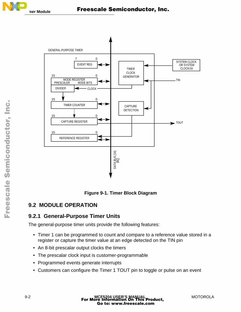
Timer Module
F
ree
sca
le S
em
ico
nd
uc
tor,
I
Freescale Semiconductor, Inc.n
c..
.
Figure 9-1. Timer Block Diagram
9.2 MODULE OPERATION
9.2.1 General-Purpose Timer UnitsThe general-purpose timer units provide the following features:
• Timer 1 can be programmed to count and compare to a reference value stored in a register or capture the timer value at an edge detected on the TIN pin
• An 8-bit prescalar output clocks the timers
• The prescalar clock input is customer-programmable
• Programmed events generate interrupts
• Customers can configure the Timer 1 TOUT pin to toggle or pulse on an event
TIMER CLOCK
GENERATOR
DIVIDER
MODE REGISTERPRESCALER MODE BITS
TIMER COUNTER
15 0
CAPTURE REGISTER
15 0
REFERENCE REGISTER
15 0
15 0
7 0
EVENT REG
CAPTURE DETECTION
SYSTEM CLOCK OR SYSTEM CLOCK/16
TIN
TOUT
DAT
A BU
S (1
6)
GENERAL-PURPOSE TIMER
CLOCK
IRQ
9-2 MCF5204 USER’S MANUAL MOTOROLA For More Information On This Product,
Go to: www.freescale.com

Timer Module
F
ree
sca
le S
em
ico
nd
uc
tor,
I
Freescale Semiconductor, Inc.n
c..
.
The maximum resolution of each timer is one system clock cycle (30 ns at 33 MHz). To obtain the maximum period, divide the system clock by 16, set the prescaler value to divide by 256, and load the reference value with ones. This maximum period is 268,435,456 cycles (8.05 seconds at 33 MHz).
9.2.1.1 PRESCALER. The prescalar clock input can be selected from the main clock (divided by 1 or by 16) or from the corresponding timer input TIN pin. TIN is synchronized to the internal clock and the synchronization delay is between two and three main clocks. TIN must meet the setup time specification shown in the Electrical Specifications section.
The CLK bits of the corresponding Timer Mode Register (TMR) select the clock input source. The prescaler is programmed to divide the clock input by values from 1 to 256. The prescalar output is used as an input to the 16-bit counter.
9.2.1.2 CAPTURE MODE. The timer has a 16-bit Timer Capture Register (TCR) that latches the counter value when the corresponding input capture edge detector senses a defined transition (of TIN). The Capture Edge (CE) bits in the TMR select the type of transition triggering the capture. A capture event sets the Timer Event Register (TER) bit and issues a maskable interrupt.
9.2.1.3 REFERENCE COMPARE. The timer can be configured to count until it reaches a reference value. It then either starts a new time count immediately or continues to run. The Free Run/Restart (FRR) bit of the TMR selects either mode. When the timer reaches the reference value, the TER bit is set and an interrupt is issued if the Output Reference Interrupt (ORI) enable bit in TMR is set.
9.2.1.4 OUTPUT MODE. The timer can send an output signal on the Timer Output (TOUT) pin when it reaches the reference value as selected by the Output Mode (OM) bit in the TMR. This signal can be an active-low pulse or a toggle of the current output under program control.
9.3 PROGRAMMING MODEL
9.3.1 General-Purpose Timer RegistersCustomers can modify the timer registers at any time. Table 9-1 illustrates the programming model.
Table 9-1. Programming Model for Timers
TIMER 1ADDRESS
TIMER 2 ADDRESS
SIM MODULE–TIMER MODULE REGISTERS
MBAR+$100 MBAR+$120 Timer Mode Register (TMR)
MBAR+$104 MBAR+$124 Timer Reference Register (TRR)
MBAR+$108 MBAR+$128 Timer Capture Register (TCR)
MBAR+$10C MBAR+$12C Timer Counter (TCN)
MBAR+$111 MBAR+$131 Reserved Timer Event Register (TER)
MOTOROLA MCF5204 USER’S MANUAL 9-3 For More Information On This Product,
Go to: www.freescale.com

Timer Module
F
ree
sca
le S
em
ico
nd
uc
tor,
I
Freescale Semiconductor, Inc.n
c..
.
9.3.1.1 TIMER MODE REGISTER (TMR). TMR is a 16-bit memory-mapped register. This register programs the various timer modes and is cleared by reset.
PS7–PS0 — Prescaler ValueThe prescaler is programmed to divide the clock input by values from 1 to 256. The value 00000000 divides the clock by 1; the value 11111111 divides the clock by 256.
CE1–CE0 — Capture Edge and Enable Interrupt11 = Capture on any edge and enable interrupt on capture event10 = Capture on falling edge only and enable interrupt on capture event 01 = Capture on rising edge only and enable interrupt on capture event 00 = Disable interrupt on capture event
OM — Output Mode 1 = Toggle output0 = Active-low pulse for one system clock cycle (30ns at 33 MHz)
ORI — Output Reference Interrupt Enable1 = Enable interrupt upon reaching the reference value0 = Disable interrupt for reference reached (does not affect interrupt on capture
function)
NOTE
If ORI is set when the REF event is asserted in the TimerEvent Register (TER), then an immediate interrupt will occur.If ORI is cleared while an interrupt is asserted, the interrupt willnegate.
FRR — Free Run/Restart1 = Restart: Timer count is reset immediately after reaching the reference value 0 = Free run: Timer count continues to increment after reaching the reference value
CLK1–CLK0 — Input Clock Source for the Timer11 = TIN pin (falling edge)10 = Master system clock divided by 16. Note that this clock source is not
synchronized to the timer; thus successive timeouts may vary slightly in length01 = Master system clock 00 =Stops counter. After the counter is stopped, the value in the Timer Counter
(TCN) register will remain constant.
Timer Mode Register (TMR) Address MBAR+$100, MBAR+$120
15 14 13 12 11 10 9 8 7 6 5 4 3 2 1 0
PRESCALER VALUE (PS7 - PS0) CE1 - CE0 OM ORI FRR ICLK1 - ICLK0 RST
RESET 0 0 0 0 0 0 0 0 0 0 0 0 0 0 0 0
Read/Write Supervisor or User Mode
9-4 MCF5204 USER’S MANUAL MOTOROLA For More Information On This Product,
Go to: www.freescale.com
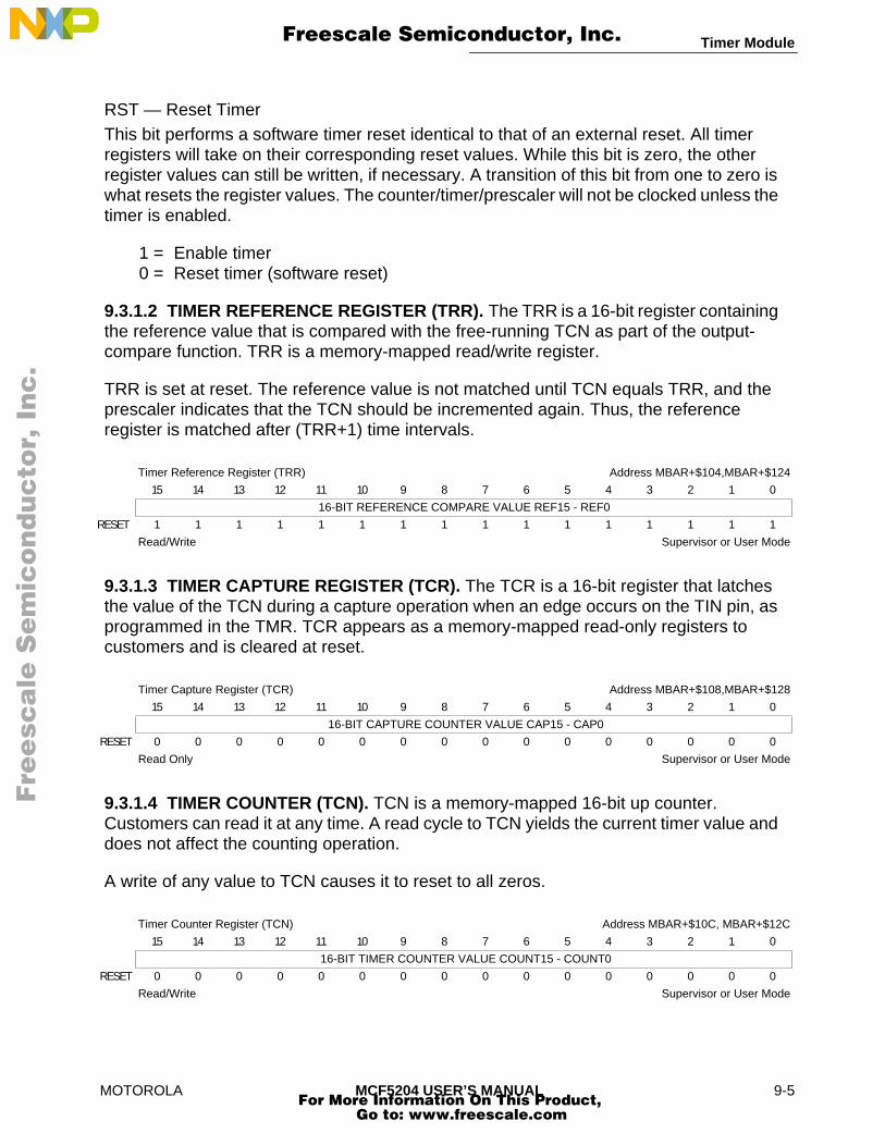
Timer Module
F
ree
sca
le S
em
ico
nd
uc
tor,
I
Freescale Semiconductor, Inc.n
c..
.
RST — Reset TimerThis bit performs a software timer reset identical to that of an external reset. All timer registers will take on their corresponding reset values. While this bit is zero, the other register values can still be written, if necessary. A transition of this bit from one to zero is what resets the register values. The counter/timer/prescaler will not be clocked unless the timer is enabled.
1 = Enable timer0 = Reset timer (software reset)
9.3.1.2 TIMER REFERENCE REGISTER (TRR). The TRR is a 16-bit register containing the reference value that is compared with the free-running TCN as part of the output-compare function. TRR is a memory-mapped read/write register.
TRR is set at reset. The reference value is not matched until TCN equals TRR, and the prescaler indicates that the TCN should be incremented again. Thus, the reference register is matched after (TRR+1) time intervals.
9.3.1.3 TIMER CAPTURE REGISTER (TCR). The TCR is a 16-bit register that latches the value of the TCN during a capture operation when an edge occurs on the TIN pin, as programmed in the TMR. TCR appears as a memory-mapped read-only registers to customers and is cleared at reset.
9.3.1.4 TIMER COUNTER (TCN). TCN is a memory-mapped 16-bit up counter. Customers can read it at any time. A read cycle to TCN yields the current timer value and does not affect the counting operation.
A write of any value to TCN causes it to reset to all zeros.
Timer Reference Register (TRR) Address MBAR+$104,MBAR+$124
15 14 13 12 11 10 9 8 7 6 5 4 3 2 1 0
16-BIT REFERENCE COMPARE VALUE REF15 - REF0
RESET 1 1 1 1 1 1 1 1 1 1 1 1 1 1 1 1
Read/Write Supervisor or User Mode
Timer Capture Register (TCR) Address MBAR+$108,MBAR+$128
15 14 13 12 11 10 9 8 7 6 5 4 3 2 1 0
16-BIT CAPTURE COUNTER VALUE CAP15 - CAP0
RESET 0 0 0 0 0 0 0 0 0 0 0 0 0 0 0 0
Read Only Supervisor or User Mode
Timer Counter Register (TCN) Address MBAR+$10C, MBAR+$12C
15 14 13 12 11 10 9 8 7 6 5 4 3 2 1 0
16-BIT TIMER COUNTER VALUE COUNT15 - COUNT0
RESET 0 0 0 0 0 0 0 0 0 0 0 0 0 0 0 0
Read/Write Supervisor or User Mode
MOTOROLA MCF5204 USER’S MANUAL 9-5 For More Information On This Product,
Go to: www.freescale.com
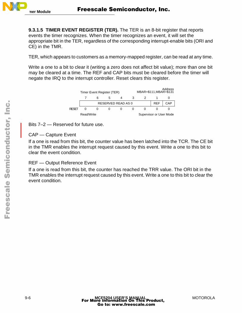
Timer Module
F
ree
sca
le S
em
ico
nd
uc
tor,
I
Freescale Semiconductor, Inc.n
c..
.
9.3.1.5 TIMER EVENT REGISTER (TER). The TER is an 8-bit register that reports events the timer recognizes. When the timer recognizes an event, it will set the appropriate bit in the TER, regardless of the corresponding interrupt-enable bits (ORI and CE) in the TMR.
TER, which appears to customers as a memory-mapped register, can be read at any time.
Write a one to a bit to clear it (writing a zero does not affect bit value); more than one bit may be cleared at a time. The REF and CAP bits must be cleared before the timer will negate the IRQ to the interrupt controller. Reset clears this register.
Bits 7–2 — Reserved for future use.
CAP — Capture Event If a one is read from this bit, the counter value has been latched into the TCR. The CE bit in the TMR enables the interrupt request caused by this event. Write a one to this bit to clear the event condition.
REF — Output Reference EventIf a one is read from this bit, the counter has reached the TRR value. The ORI bit in the TMR enables the interrupt request caused by this event. Write a one to this bit to clear the event condition.
Timer Event Register (TER)Address
MBAR+$111,MBAR+$131
7 6 5 4 3 2 1 0
RESERVED READ AS 0 REF CAP
RESET 0 0 0 0 0 0 0 0
Read/Write Supervisor or User Mode
9-6 MCF5204 USER’S MANUAL MOTOROLA For More Information On This Product,
Go to: www.freescale.com

DATE: 08-21-98
REVISION NO: 0.1
PAGES AFFECTED: SEE CHANGE BARS
F
ree
sca
le S
em
ico
nd
uc
tor,
I
Freescale Semiconductor, Inc.n
c..
.
SECTION 10DEBUG SUPPORT
This section details the hardware debug support functions within the ColdFire 5200 Family of processors.
The general topic of debug support has been divided into three separate areas:
1. Real-Time Trace Support
2. Background Debug Mode (BDM)
3. Real-Time Debug Support
Each of the three areas is addressed in detail in the following subsections.
The logic required to support these three areas is contained in a Debug module, which is shown in the system block diagram in Figure 10-1.
10.1 REAL-TIME TRACEIn the area of debug functions, one fundamental requirement is support for real-time trace functionality (i.e., definition of the dynamic execution path). The ColdFire solution is to include a parallel output port providing encoded processor status and data to an external development system. This port is partitioned into two 4-bit nibbles: one nibble allows the processor to transmit information concerning the execution status of the core (processor status, PST[3:0]), while the other nibble allows data to be displayed (debug data, DDATA[3:0]).
Figure 10-1. Processor/Debug Module Interface
COLDFIRE CPU
DEBUG
MODULE
BDM PORT
DDATA, PST DSCLK, DSI, DSO
INTERNAL BUSESCORE
TRACE PORT
MOTOROLA MCF5204 USER’S MANUAL 10-1 For More Information On This Product,
Go to: www.freescale.com

Debug SupportDebug Support
F
ree
sca
le S
em
ico
nd
uc
tor,
I
Freescale Semiconductor, Inc.n
c..
.
The processor status timing is synchronous with the processor clock (CLK) and the status may not be related to the current bus transfer. Table 10-1 below shows the encodings of these signals.
The processor status outputs can be used with an external image of the program to completely track the dynamic execution path of the machine. The tracking of this dynamic path is complicated by any change-of-flow operation. Within the ColdFire instruction set architecture, most branch instructions are implemented using PC-relative addressing. Accordingly, the external program image can determine branch target addresses. Additionally, there are a number of instructions that use some type of variant addressing, i.e., the calculation of the target instruction address is not PC-relative or absolute, but involves the use of a program-visible register.
The simplest example of a branch instruction using a variant addressing mode is the compiled code for a C language case statement. Typically, the evaluation of this statement uses the variable of an expression as an index into a table of offsets, where each offset points to a unique case within the structure. For these types of change-of-flow operations, the ColdFire processor uses the debug pins to output a sequence of information.
1. Identify a taken branch has been executed using the PST[3:0]=$5.
2. Using the PST pins, signal the target address is to be displayed on the DDATA pins. The encoding identifies the number of bytes that are displayed and is optional.
3. The new target address is optionally available on subsequent cycles using the nibble-wide DDATA port. The number of bytes of the target address displayed on this port is a configurable parameter (2, 3, or 4 bytes).
Table 10-1. Processor PST Definition
PST[3:0] DEFINITION
0000 Continue execution
0001 Begin execution of an instruction
0010 Reserved
0011 Entry into user-mode
0100 Begin execution of PULSE or WDDATA instruction
0101 Begin execution of taken branch
0110 Reserved
0111 Begin execution of RTE instruction
1000 Begin 1-byte transfer on DData
1001 Begin 2-byte transfer on DData
1010 Begin 3-byte transfer on DData
1011 Begin 4-byte transfer on DData
1100 † Exception processing
1101 † Emulator-mode entry exception processing
1110 † Processor is stopped, waiting for interrupt
1111 † Processor is halted
† These encodings are asserted for multiple cycles.
10-2 MCF5204 USER’S MANUAL MOTOROLA For More Information On This Product,
Go to: www.freescale.com

Debug Support
F
ree
sca
le S
em
ico
nd
uc
tor,
I
Freescale Semiconductor, Inc.n
c..
.
The nibble-wide DDATA port includes two 32-bit storage elements for capturing the CPU core bus information. These two elements effectively form a FIFO buffer connecting the core bus to the external development system. The FIFO buffer captures variant branch target addresses along with certain operand read/write data for eventual display on the DDATA output port. The execution speed of the ColdFire processor is affected only when both storage elements contain valid data waiting to be dumped onto the DDATA port. In this case, the processor core is stalled until one FIFO entry is available. In all other cases, data output on the DDATA port does not impact execution speed.
From the processor core perspective, the PST outputs signal the first AGEX cycle of an instruction’s execution. Most single-cycle instructions begin and complete their execution within a given machine cycle.
Because the processor status (PST[3:0]) values of $C, $D, $E and $F define a multicycle mode or a special operation, the PST outputs are driven with these values until the mode is exited or the operation completed. All the remaining fields specify information that is updated each machine cycle.
The status values of $8, $9, $A and $B qualify the contents of the DDATA output bus. These encodings are driven onto the PST port one machine cycle before the actual data is displayed on DDATA.
Figure 10-2 shows the execution of an indirect JMP instruction with the lower 16 bits of the target address being displayed on the DDATA output. In this diagram, the indirect JMP branches to address “target.” The processor internally forms the PST marker ($9) one cycle before the address begins to appear on the DDATA port. The target address is displayed on DDATA for four consecutive clocks, starting with the least-significant nibble. The processor continues execution, unaffected by the DDATA bus activity.
Figure 10-2. Pipeline Timing Example - Debug Output
LAST DSOC AGEX
JMP (A0) DSOC AGEX
TARGET IAG IC DSOC AGEX
TARGET + $4 IAG IC DSOC AGEX
INTERNAL PST $5 $9 $0 TARGET
INTERNAL DDATA $0 $0 3:0 7:4 11:8 15:12
PST PINS $5 $9 $0 TARGET
DDATA PINS $0 $0 3:0 7:4 11:8 15:12
MOTOROLA MCF5204 USER’S MANUAL 10-3 For More Information On This Product,
Go to: www.freescale.com

Debug SupportDebug Support
F
ree
sca
le S
em
ico
nd
uc
tor,
I
Freescale Semiconductor, Inc.n
c..
.
The ColdFire instruction set architecture (ISA) includes a PULSE opcode. This opcode generates a unique PST encoding when executed (PST = $4). This instruction can define logic analyzer triggers for debug and/or performance analysis.
Additionally, a WDDATA opcode is supported that allows the processor core to write any operand (byte, word, long) directly to the DDATA port, independent of any Debug module configuration. This opcode also generates the special PST = $4 encoding when executed.
10.2 BACKGROUND-DEBUG MODE (BDM)ColdFire 5200 processors support a modified version of the background-debug mode (BDM) functionality found on Motorola’s CPU32 Family of parts. BDM implements a low-level system debugger in the microprocessor hardware. Communication with the development system is handled via a dedicated, high-speed serial command interface (BDM port).
Unless noted otherwise, the BDM functionality provided by ColdFire 5200 processors is a proper subset of the CPU32 functionality. The main differences include the following:
• ColdFire implements the BDM controller in a dedicated hardware module. Although some BDM operations do require the CPU to be halted (e.g., CPU register accesses), other BDM commands such as memory accesses can be executed while the processor is running.
• DSCLK, DSI, and DSO are treated as synchronous signals, where the inputs (DSCLK and DSI) must meet the required input setup and hold timings, and the output (DSO) is specified as a delay relative to the rising edge of the processor clock.
• On CPU32 parts, DSO could signal hardware that a serial transfer can start. ColdFire clocking schemes restrict the use of this bit. Because DSO changes only when DSCLK is high, DSO cannot be used to indicate the start of a serial transfer. The development system should use either a free-running DSCLK or count the number of clocks in any given transfer.
• The Read/Write System Register commands (RSREG/WSREG) have been replaced by Read/Write Control Register commands (RCREG/WCREG). These commands use the register coding scheme from the MOVEC instruction.
• Read/Write Debug Module Register commands (RDMREG/WDMREG) have been add-ed to support Debug module register accesses.
• CALL and RST commands are not supported.
• Illegal command responses can be returned using the FILL and DUMP commands.
• For any command performing a byte-sized memory read operation, the upper 8 bits of the response data are undefined. The referenced data is returned in the lower 8 bits of the response.
• The Debug module forces alignment for memory-referencing operations: long accesses are forced to a 0-modulo-4 address; word accesses are forced to a 0-modulo-2 address. An address error response can no longer be returned.
10-4 MCF5204 USER’S MANUAL MOTOROLA For More Information On This Product,
Go to: www.freescale.com

Debug Support
F
ree
sca
le S
em
ico
nd
uc
tor,
I
Freescale Semiconductor, Inc.n
c..
.
10.2.1 CPU HaltAlthough some BDM operations can occur in parallel with CPU operation, unrestricted BDM operation requires the CPU to be halted. A number of sources can cause the CPU to halt, including the following (as shown in order of priority):
1. The occurrence of the catastrophic fault-on-fault condition automatically halts the processor. The halt status is posted on the PST port ($F).
2. The occurrence of a hardware breakpoint (reference subsection 10.3 Real-Time Debug Support ) can be configured to generate a pending halt condition in a manner similar to the assertion of the BKPT signal. In some cases, the occurrence of this type of breakpoint halts the processor in an imprecise manner. Once the hardware breakpoint is asserted, the processor halts at the next sample point. See subsection 10.3.2 Theory of Operation for more detail.
3. The execution of the HALT (also known as BGND on the 683xx devices) instruction immediately suspends execution and posts the halt status ($F) on the PST outputs. By default, this is a supervisor instruction and attempted execution while in user mode generates a privilege-violation exception. A User Halt Enable (UHE) control bit is provided in the Configuration/Status Register (CSR) to allow execution of HALT in user mode.
4. The assertion of the BKPT input pin is treated as an pseudo-interrupt, i.e., the halt condition is made pending until the processor core samples for halts/interrupts. The processor samples for these conditions once during the execution of each instruction. If there is a pending halt condition at the sample time, the processor suspends execution and enters the halted state. The halt status ($F) is reflected in the PST outputs.
The halt source is indicated in CSR[27:24]; for simultaneous halt conditions, the highest priority source is indicated.
There are two special cases involving the assertion of the BKPT pin to be considered, which are explained next.
After RSTI is negated, the processor waits for 16 clock cycles before beginning reset exception processing. If the BKPT input pin is asserted within the first eight cycles after RSTI is negated, the processor will enter the halt state, signaling that status on the PST outputs ($F). While in this state, all resources accessible via the Debug module can be referenced. Once the system initialization is complete, the processor response to a BDM GO command depends on the set of BDM commands performed while “breakpointed.” Specifically, if the processor’s PC register was loaded, the GO command causes the processor to exit the halt state and pass control to the instruction address contained in the PC. In this case, the normal reset exception processing is bypassed. Conversely, if the PC register was not loaded, the GO BDM command causes the processor to exit the halt state and continue with reset exception processing.
ColdFire 5200 processors also handle a special case with the assertion of BKPT while the processor is stopped by execution of the STOP instruction. For this case when the BKPT is asserted, the processor exits the stopped mode and enters the halted state. Once halted,
MOTOROLA MCF5204 USER’S MANUAL 10-5 For More Information On This Product,
Go to: www.freescale.com

Debug SupportDebug Support
F
ree
sca
le S
em
ico
nd
uc
tor,
I
Freescale Semiconductor, Inc.n
c..
.
the standard BDM commands may be exercised. When the processor is restarted, it continues with the execution of the next sequential instruction, i.e., the instruction following the STOP opcode.
The Debug module Configuration/Status Register (CSR) maintains status defining the condition that caused the CPU to halt.
10.2.2 BDM Serial InterfaceOnce the CPU is halted and the halt status reflected on the PST outputs (PST[3:0]=$F), the development system can send unrestricted commands to the Debug module. The Debug module implements a synchronous protocol using a three-pin interface: development serial clock (DSCLK), development serial input (DSI), and development serial output (DSO). The development system serves as the serial communication channel master and is responsible for generation of the clock (DSCLK). The operating range of the serial channel is DC to one-half of the processor frequency. The channel uses a full duplex mode, where data is transmitted and received simultaneously by both master and slave devices.
Both DSCLK and DSI are synchronous inputs and must meet input setup and hold times with respect to CLK. DSCLK essentially acts as a pseudo “clock enable” and is sampled on the rising edge of CLK. If the setup time of DSCLK is met, then the internal logic transitions on the rising edge of CLK, and DSI is sampled on the same CLK rising edge. The DSO output is specified as a delay from the DSCLK-enabled CLK rising edge. All events in the Debug module’s serial state machine are based on the rising edge of the microprocessor clock (see Figure 10-3 below). Refer to Section 12 Electrical Characteristics.
Figure 10-3. BDM Signal Sampling
The basic packet of information is a 17-bit word (16 data bits plus a status/control bit), as shown below.
16 15 0
S/C DATA FIELD [15:0]
CLK
DSCLK
DSI
DSO
10-6 MCF5204 USER’S MANUAL MOTOROLA For More Information On This Product,
Go to: www.freescale.com

Debug Support
F
ree
sca
le S
em
ico
nd
uc
tor,
I
Freescale Semiconductor, Inc.n
c..
.
Status/ControlThe status/control bit indicates the status of CPU-generated messages (always single word with the data field encoded as listed in Table 10-2). Command and data transfers initiated by the development system should clear bit 16. The current implementation ignores this bit; however, Motorola has reserved this bit for future enhancements.
Data FieldThe data field contains the message data to be communicated between the development system and the Debug module.
10.2.3 BDM Command SetColdFire 5200 processors support a subset of BDM instructions from the current 683xx parts, as well as extensions to provide access to new hardware features.
10.2.3.1 BDM COMMAND SET SUMMARY. The BDM command set is summarized in Table 10-3. Subsequent paragraphs contain detailed descriptions of each command.
Table 10-2. CPU-Generated Message EncodingS/C BIT DATA MESSAGE TYPE
0 xxxx Valid data transfer0 $FFFF Command complete; status OK1 $0000 Not ready with response; come again1 $0001 TEA-terminated bus error cycle; data invalid1 $FFFF Illegal command
Table 10-3. BDM Command Summary
COMMAND MNEMONIC DESCRIPTIONCPU
IMPACT1 PAGE
Read A/D Register RAREG/RDREG Read the selected address or data register and return the resultvia the serial BDM interface Halted 6-10
Write A/D Register WAREG/WDREG The data operand is written to the specified address or data register via the serial BDM interface Halted 6-11
Read Memory Location READ Read the sized data at the memory location specified by thelongword address
CycleSteal 6-12
Write Memory Location WRITE Write the operand data to the memory location specified by the longword address
CycleSteal 6-14
Dump Memory Block DUMP
Used in conjunction with the READ command to dump largeblocks of memory. An initial READ is executed to set up thestarting address of the block and to retrieve the first result.Subsequent operands are retrieved with the DUMP command.
CycleSteal 6-16
Fill Memory Block FILL
Used in conjunction with the WRITE command to fill largeblocks of memory. An initial WRITE is executed to set up thestarting address of the block and to supply the first operand.Subsequent operands are written with the FILL command.
CycleSteal 6-18
Resume Execution GO The pipeline is flushed and refilled before resuming instructionexecution at the current PC Halted 6-20
No Operation NOP NOP performs no operation and may be used as a null command Parallel 6-20
Read Control Register RCREG Read the system control register Halted 6-21Write Control Register WCREG Write the operand data to the system control register Halted 6-22Read Debug Module
Register RDMREG Read the Debug module register Parallel 6-23
MOTOROLA MCF5204 USER’S MANUAL 10-7 For More Information On This Product,
Go to: www.freescale.com

Debug SupportDebug Support
F
ree
sca
le S
em
ico
nd
uc
tor,
I
Freescale Semiconductor, Inc.n
c..
.
10.2.3.2 COLDFIRE BDM COMMANDS. All ColdFire Family BDM commands include a 16-bit operation word followed by an optional set of one or more extension words.
Operation FieldThe operation field specifies the command.
R/W FieldThe R/W field specifies the direction of operand transfer. When the bit is set, the transfer is from the CPU to the development system. When the bit is cleared, data is written to the CPU or to memory from the development system.
Operand SizeFor sized operations, this field specifies the operand data size. All addresses are expressed as 32-bit absolute values. The size field is encoded as listed in Table 10-4.
Address / Data (A/D) FieldThe A/D field is used in commands that operate on address and data registers in the processor. It determines whether the register field specifies a data or address register. A one indicates an address register; zero, a data register.
Register FieldIn commands that operate on processor registers, this field specifies which register is selected. The field value contains the register number.
Write Debug Module Register WDMREG Write the operand data to the Debug module register Halted 6-23
NOTE:
1. General command effect and/or requirements on CPU operation:
Halted - The CPU must be halted to perform this command
Steal - Command generates a bus cycle which is interleaved with CPU accesses
Parallel - Command is executed in parallel with CPU activity
Refer to command summaries for detailed operation descriptions.
15 10 9 8 7 6 5 4 3 2 0
OPERATION 0 R/W OP SIZE 0 0 A/D REGISTER
EXTENSION WORD(S)
Table 10-4. BDM Size Field EncodingENCODING OPERAND SIZE
00 Byte01 Word10 Long11 Reserved
Table 10-3. BDM Command Summary (Continued)
COMMAND MNEMONIC DESCRIPTIONCPU
IMPACT1 PAGE
10-8 MCF5204 USER’S MANUAL MOTOROLA For More Information On This Product,
Go to: www.freescale.com

Debug Support
F
ree
sca
le S
em
ico
nd
uc
tor,
I
Freescale Semiconductor, Inc.n
c..
.
Extension Word(s) (as required):Certain commands require extension words for addresses and/or immediate data. Addresses require two extension words because only absolute long addressing is permitted. Immediate data can be either one or two words in length; byte and word data each require a single extension word; longword data requires two words. Both operands and addresses are transferred by most significant word first. In the following descriptions of the BDM command set, the optional set of extension words are defined as the “Operand Data.”
10.2.3.3 Command Sequence Diagram. A command sequence diagram (see Figure 10-4) illustrates the serial bus traffic for each command. Each bubble in the diagram represents a single 17-bit transfer across the bus. The top half in each diagram corresponds to the data transmitted by the development system to the Debug module; the bottom half corresponds to the data returned by the Debug module in response to the development system commands. Command and result transactions are overlapped to minimize latency.
The cycle in which the command is issued contains the development system command mnemonic (in this example, “read memory location”). During the same cycle, the Debug module responds with either the lowest order results of the previous command or with a command complete status (if no results were required).
During the second cycle, the development system supplies the high-order 16 bits of the memory address. The Debug module returns a “not ready” response($10000) unless the received command was decoded as unimplemented, in which case the response data is the illegal command ($1FFFF) encoding. If an illegal command response occurs, the development system should retransmit the command.
NOTE
The “not ready” response can be ignored unless a memory buscycle is in progress. Otherwise, the Debug module can accept anew serial transfer after eight system clock periods.
In the third cycle, the development system supplies the low-order 16 bits of a memory address. The Debug module always returns the “not ready” response in this cycle. At the completion of the third cycle, the Debug module initiates a memory read operation. Any serial transfers that begin while the memory access is in progress return the “not ready” response.
Results are returned in the two serial transfer cycles following the completion of memory access. The data transmitted to the Debug module during the final transfer is the opcode for the following command. Should a memory access generate a bus error, an error status ($10001) is returned in place of the result data.
MOTOROLA MCF5204 USER’S MANUAL 10-9 For More Information On This Product,
Go to: www.freescale.com

Debug SupportDebug Support
F
ree
sca
le S
em
ico
nd
uc
tor,
I
Freescale Semiconductor, Inc.n
c..
.
Figure 10-4. Command Sequence Diagram
10.2.3.4 Command Set Descriptions. The BDM command set is summarized on pages 10-7 and 10-8.
Note
All the accompanying valid BDM results are defined with themost significant bit of the 17-bit response (S/C) as 0. Invalidcommand responses (Not Ready; TEA-terminated bus cycle; Il-legal Command) return a 1 in the most significant bit of the 17-bit response (S/C).
Unassigned command opcodes are reserved by Motorola for future expansion.
10.2.3.4.1 Read A/D Register (RAREG/RDREG). Read the selected address or data register and return the 32-bit result. A bus error response is returned if the CPU core is not halted.
COMMANDS TRANSMITTED TO THE DEBUG MODULE
COMMAND CODE TRANSMITTED DURING THIS CYCLE
HIGH-ORDER 16 BITS OF MEMORY ADDRESS
LOW-ORDER 16 BITS OF MEMORY ADDRESS
SEQUENCE TAKEN IFOPERATION HAS NOTCOMPLETED
DATA UNUSED FROMTHIS TRANSFER
SEQUENCE TAKEN IFILLEGAL COMMANDIS RECEIVED BY DEBUG MODULE
RESULTS FROM PREVIOUS COMMAND
RESPONSES FROM THE DEBUG MODULE
NONSERIAL-RELATED ACTIVITY
MS ADDR"NOT READY"
XXX"ILLEGAL"
LS ADDR"NOT READY"
NEXT CMD"NOT READY"
READ (LONG)???
NEXT CMD"NOT READY"
XXX"NOT READY"
XXXXX
XXXBERR
MS RESULTNEXT CMDLS RESULT
READMEMORY
LOCATION
NEXTCOMMAND
CODE
SEQUENCE TAKEN IF BUS ERROR OCCURS ONMEMORY ACCESS
HIGH- AND LOW-ORDER16 BITS OF RESULT
XXX
10-10 MCF5204 USER’S MANUAL MOTOROLA For More Information On This Product,
Go to: www.freescale.com

Debug Support
F
ree
sca
le S
em
ico
nd
uc
tor,
I
Freescale Semiconductor, Inc.n
c..
.
Formats:
Command Sequence:
Operand Data:None
Result Data:The contents of the selected register are returned as a longword value. The data is returnedmost significant word first.
10.2.3.4.2 Write A/D Register (WAREG/WDREG). The operand (longword) data is written to the specified address or data register. All 32 register bits are altered by the write. A bus error response is returned if the CPU core is not halted.
15 14 13 12 11 10 9 8 7 6 5 4 3 2 1 0
$2 $1 $8 A/D REGISTER
RAREG/RDREG Command
15 14 13 12 11 10 9 8 7 6 5 4 3 2 1 0
DATA [31:16]
DATA [15:0]
RAREG/RDREG Result
XXXMS RESULT
NEXT CMDLS RESULT
RAREG/RDREG???
XXXBERR
NEXT CMD"NOT READY"
MOTOROLA MCF5204 USER’S MANUAL 10-11 For More Information On This Product,
Go to: www.freescale.com

Debug SupportDebug Support
F
ree
sca
le S
em
ico
nd
uc
tor,
I
Freescale Semiconductor, Inc.n
c..
.
Command Formats:
Command Sequence:
Operand Data:Longword data is written into the specified address or data register. The data is suppliedmost significant word first.
Result Data:Command complete status ($0FFFF) is returned when register write is complete.
10.2.3.4.3 Read Memory Location (READ). Read the operand data from the memory location specified by the longword address. The address space is defined by the contents of the low-order 5 bits {TT, TM} of the address attribute register (AATR). The hardware forces the low-order bits of the address to zeros for word and longword accesses to ensure that operands are always accessed on natural boundaries: words on 0-modulo-2 addresses, longwords on 0-modulo-4 addresses.
15 14 13 12 11 10 9 8 7 6 5 4 3 2 1 0
$2 $0 $8 A/D REGISTER
DATA [31:16]
DATA [15:0]
WAREG/WDREG Command
MS DATA"NOT READY"
XXX
LS DATA"NOT READY"
NEXT CMD"NOT READY"
WDREG/WAREG???
NEXT CMD"CMD COMPLETE"
BERR
10-12 MCF5204 USER’S MANUAL MOTOROLA For More Information On This Product,
Go to: www.freescale.com

Debug Support
F
ree
sca
le S
em
ico
nd
uc
tor,
I
Freescale Semiconductor, Inc.n
c..
.
Formats:
15 14 13 12 11 10 9 8 7 6 5 4 3 2 1 0
$1 $9 $0 $0
ADDRESS [31:16]
ADDRESS [15:0]
Byte READ Command
15 14 13 12 11 10 9 8 7 6 5 4 3 2 1 0
X X X X X X X X DATA [7:0]
Byte READ Result
15 14 13 12 11 10 9 8 7 6 5 4 3 2 1 0
$1 $9 $4 $0
ADDRESS [31:16]
ADDRESS [15:0]
Word READ Command
15 14 13 12 11 10 9 8 7 6 5 4 3 2 1 0
DATA [15:0]
Word READ Result
15 14 13 12 11 10 9 8 7 6 5 4 3 2 1 0
$1 $9 $8 $0
ADDRESS [31:16]
ADDRESS [15:0]
Long READ Command
15 14 13 12 11 10 9 8 7 6 5 4 3 2 1 0
DATA [31:16]
DATA [15:0]
Long READ Result
MOTOROLA MCF5204 USER’S MANUAL 10-13 For More Information On This Product,
Go to: www.freescale.com

Debug SupportDebug Support
F
ree
sca
le S
em
ico
nd
uc
tor,
I
Freescale Semiconductor, Inc.n
c..
.
Command Sequence:
Operand Data:The single operand is the longword address of the requested memory location.
Result Data:The requested data is returned as either a word or longword. Byte data is returned in theleast significant byte of a word result, with the upper byte undefined. Word results return 16bits of significant data; longword results return 32 bits.
A successful read operation returns data bit 16 cleared. If a bus error is encountered, thereturned data is $10001.
10.2.3.4.4 Write Memory Location (WRITE). Write the operand data to the memory location specified by the longword address. The address space is defined by the contents of the low-order 5 bits {TT, TM} of the address attribute register (AATR). The hardware forces the low-order bits of the address to zeros for word and longword accesses to ensure that operands are always accessed on natural boundaries: words on 0-modulo-2 addresses, longwords on 0-modulo-4 addresses.
Formats:
15 14 13 12 11 10 9 8 7 6 5 4 3 2 1 0
$1 $8 $0 $0
ADDRESS [31:16]
ADDRESS [15:0]
X X X X X X X X DATA [7:0]
Byte WRITE Command
MS ADDR"NOT READY"
LS ADDR"NOT READY"
READ (B/W)???
NEXT CMD"NOT READY"
XXX"NOT READY"
XXX
XXXBERR
RESULTNEXT CMD
READMEMORY
LOCATION
MS ADDR"NOT READY"
LS ADDR"NOT READY"
READ (LONG)???
NEXT CMD"NOT READY"
XXX"NOT READY"
XXX
XXXBERR
MS RESULTXXX
READMEMORY
LOCATION
NEXT CMDLS RESULT
10-14 MCF5204 USER’S MANUAL MOTOROLA For More Information On This Product,
Go to: www.freescale.com

Debug Support
F
ree
sca
le S
em
ico
nd
uc
tor,
I
Freescale Semiconductor, Inc.n
c..
.
Command Sequence:
Operand Data:Two operands are required for this instruction. The first operand is a longword absolute ad-dress that specifies a location to which the operand data is to be written. The second oper-and is the data. Byte data is transmitted as a 16-bit word, justified in the least significant byte;16- and 32-bit operands are transmitted as 16 and 32 bits, respectively.
15 14 13 12 11 10 9 8 7 6 5 4 3 2 1 0
$1 $8 $4 $0
ADDRESS [31:16]
ADDRESS [15:0]
DATA [15:0]
Word WRITE Command
15 14 13 12 11 10 9 8 7 6 5 4 3 2 1 0
$1 $8 $8 $0
ADDRESS [31:16]
ADDRESS [15:0]
DATA [31:16]
DATA [15:0]
Long WRITE Command
MS ADDR"NOT READY"
LS ADDR"NOT READY"
WRITE (B/W)???
NEXT CMD"NOT READY"
XXX"NOT READY"
XXX
XXXBERR
"CMD COMPLETE"NEXT CMD
WRITEMEMORY
LOCATION
DATA"NOT READY"
MS ADDR"NOT READY"
LS ADDR"NOT READY"
WRITE (LONG)???
NEXT CMD"NOT READY"
XXX"NOT READY"
XXX
XXXBERR
"CMD COMPLETE"NEXT CMD
WRITEMEMORY
LOCATION
MS DATA"NOT READY"
LS DATA"NOT READY"
MOTOROLA MCF5204 USER’S MANUAL 10-15 For More Information On This Product,
Go to: www.freescale.com

Debug SupportDebug Support
F
ree
sca
le S
em
ico
nd
uc
tor,
I
Freescale Semiconductor, Inc.n
c..
.
Result Data:Successful write operations return a status of $0FFFF. A bus error on the write cycle is in-dicated by the assertion of bit 16 in the status message and by a data pattern of $0001.
10.2.3.4.5 Dump Memory Block (DUMP). DUMP is used in conjunction with the READ command to dump large blocks of memory. An initial READ is executed to set up the starting address of the block and to retrieve the first result. The DUMP command retrieves subsequent operands. The initial address is incremented by the operand size (1, 2, or 4) and saved in a temporary register (Address Breakpoint High (ABHR)). Subsequent DUMP commands use this address, perform the memory read, increment it by the current operand size, and store the updated address in ABHR.
NOTE
The DUMP command does not check for a valid address inABHR—DUMP is a valid command only when preceded byanother DUMP, NOP or by a READ command. Otherwise, anillegal command response is returned. The NOP command canbe used for intercommand padding without corrupting theaddress pointer.
The size field is examined each time a DUMP command is given, allowing the operand size to be dynamically altered.
10-16 MCF5204 USER’S MANUAL MOTOROLA For More Information On This Product,
Go to: www.freescale.com
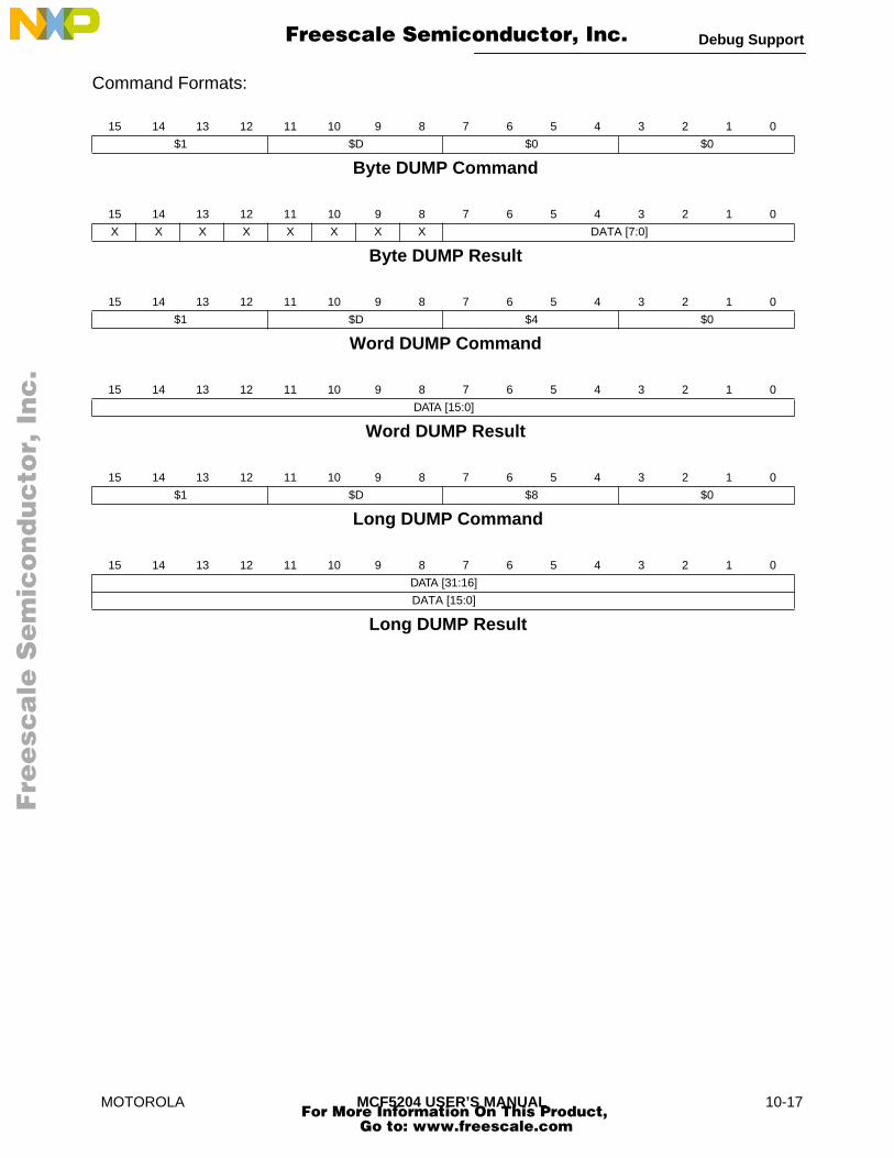
Debug Support
F
ree
sca
le S
em
ico
nd
uc
tor,
I
Freescale Semiconductor, Inc.n
c..
.
Command Formats:
15 14 13 12 11 10 9 8 7 6 5 4 3 2 1 0
$1 $D $0 $0
Byte DUMP Command
15 14 13 12 11 10 9 8 7 6 5 4 3 2 1 0
X X X X X X X X DATA [7:0]
Byte DUMP Result
15 14 13 12 11 10 9 8 7 6 5 4 3 2 1 0
$1 $D $4 $0
Word DUMP Command
15 14 13 12 11 10 9 8 7 6 5 4 3 2 1 0
DATA [15:0]
Word DUMP Result
15 14 13 12 11 10 9 8 7 6 5 4 3 2 1 0
$1 $D $8 $0
Long DUMP Command
15 14 13 12 11 10 9 8 7 6 5 4 3 2 1 0
DATA [31:16]
DATA [15:0]
Long DUMP Result
MOTOROLA MCF5204 USER’S MANUAL 10-17 For More Information On This Product,
Go to: www.freescale.com

Debug SupportDebug Support
F
ree
sca
le S
em
ico
nd
uc
tor,
I
Freescale Semiconductor, Inc.n
c..
.
Command Sequence:
Operand Data:None
Result Data:Requested data is returned as either a word or longword. Byte data is returned in the leastsignificant byte of a word result. Word results return 16 bits of significant data; longword re-sults return 32 bits. Status of the read operation is returned as in the READ command:$0xxxx for success, $10001 for a bus error.
10.2.3.4.6 Fill Memory Block (FILL). FILL is used in conjunction with the WRITE command to fill large blocks of memory. An initial WRITE is executed to set up the starting address of the block and to supply the first operand. The FILL command writes subsequent operands. The initial address is incremented by the operand size (1, 2, or 4) and is saved in ABHR after the memory write. Subsequent FILL commands use this address, perform the write, increment it by the current operand size, and store the updated address in ABHR.
NOTE
The FILL command does not check for a valid address inABHR—FILL is a valid command only when preceded byanother FILL, NOP or by a WRITE command. Otherwise, anillegal command response is returned. The NOP command canbe used for intercommand padding without corrupting theaddress pointer.
The size field is examined each time a FILL command is processed, allowing the operand size to be altered dynamically.
XXX"NOT READY"
NEXT CMD RESULT
XXXBERR
XXX"ILLEGAL"
NEXT CMD"NOT READY"
NEXT CMD"NOT READY"
READMEMORY
LOCATION
DUMP (B/W)???
XXX"NOT READY"
NEXT CMD MS RESULT
XXXBERR
XXX"ILLEGAL"
NEXT CMD"NOT READY"
NEXT CMD"NOT READY"
READMEMORY
LOCATION
DUMP (LONG)???
NEXT CMDLS RESULT
10-18 MCF5204 USER’S MANUAL MOTOROLA For More Information On This Product,
Go to: www.freescale.com

Debug Support
Fre
esc
ale
Se
mic
on
du
cto
r, I
Freescale Semiconductor, Inc.n
c..
.
Formats:
Command Sequence:
Operand Data:A single operand is data to be written to the memory location. Byte data is transmitted as a16-bit word, justified in the least significant byte; 16- and 32-bit operands are transmitted as16 and 32 bits, respectively.
Result Data:Status is returned as in the WRITE command: $0FFFF for a successful operation and$10001 for a bus error during a write.
15 14 13 12 11 10 9 8 7 6 5 4 3 2 1 0
$1 $C $0 $0
X X X X X X X X DATA [7:0]
Byte FILL Command
15 14 13 12 11 10 9 8 7 6 5 4 3 2 1 0
$1 $C $4 $0
DATA [15:0]
Word FILL Command
15 14 13 12 11 10 9 8 7 6 5 4 3 2 1 0
$1 $C $8 $0
DATA [31:16]
DATA [15:0]
Long FILL Command
NEXT CMD"NOT READY"
"NOT READY"
XXXBERR
"CMD COMPLETE"
DATA"NOT READY"
XXX
NEXT CMDXXX"ILLEGAL"
NEXT CMD"NOT READY"
FILL (LONG)???
WRITEMEMORY
LOCATION
NEXT CMD"NOT READY"
XXX"NOT READY"
XXXBERR
"CMD COMPLETE"
MS DATA"NOT READY"
NEXT CMDXXX"ILLEGAL"
NEXT CMD"NOT READY"
LS DATA"NOT READY"
WRITEMEMORY
LOCATION
FILL (B/W)???
(LONG)
(B/W)
MOTOROLA MCF5204 USER’S MANUAL 10-19 For More Information On This Product,
Go to: www.freescale.com

Debug SupportDebug Support
Fre
esc
ale
Se
mic
on
du
cto
r, I
Freescale Semiconductor, Inc.n
c..
.
10.2.3.4.7 Resume Execution (GO). The pipeline is flushed and refilled before resuming normal instruction execution. Prefetching begins at the current PC and current privilege level. If either the PC or SR is altered during BDM, the updated value of these registers is used when prefetching begins.
Formats:
Command Sequence:
Operand Data:None
Result Data:The “command complete” response ($0FFFF) is returned during the next shift operation.
10.2.3.4.8 No Operation (NOP). NOP performs no operation and can be used as a null command, where required.
Formats:
Command Sequence:
Operand Data:None
15 14 13 12 11 10 9 8 7 6 5 4 3 2 1 0
$0 $C $0 $0
GO Command
15 12 11 8 7 4 3 0
$0 $0 $0 $0
NOP Command
GO???
NEXT CMD"CMD COMPLETE"
NOP???
NEXT CMD"CMD COMPLETE"
10-20 MCF5204 USER’S MANUAL MOTOROLA For More Information On This Product,
Go to: www.freescale.com

Debug Support
Fre
esc
ale
Se
mic
on
du
cto
r, I
Freescale Semiconductor, Inc.n
c..
.
Result Data:The “command complete” response ($0FFFF) is returned during the next shift operation.
10.2.3.4.9 Read Control Register (RCREG). Read the selected control register and return the 32-bit result. Accesses to the processor/memory control registers are always 32 bits in size, regardless of the implemented register width. The second and third words of the command effectively form a 32-bit address the Debug module uses to generate a special bus cycle to access the specified control register. The 12-bit Rc field is the same as that used by the MOVEC instruction.
Formats
Rc encoding:
Command Sequence:
15 14 13 12 11 10 9 8 7 6 5 4 3 2 1 0
$2 $9 $8 $0
$0 $0 $0 $0
$0 RC
RCREG Command
15 14 13 12 11 10 9 8 7 6 5 4 3 2 1 0
DATA [31:16]
DATA [15:0]
RCREG Result
Table 10-5. Control Register MapRc REGISTER DEFINITION
$002 Cache Control Register (CACR)$004 Access Control Unit 0 (ACR0)$005 Access Control Unit 1 (ACR1)$801 Vector Base Register (VBR)$80E Status Register (SR)$80F Program Counter (PC)$C04 RAM Base Address Register (RAMBAR)$C0F Module Base Address Register (MBAR)
EXT WORD"NOT READY"
EXT WORD"NOT READY"
RCREG???
NEXT CMD"NOT READY"
XXX"NOT READY"
XXX
XXXBERR
MS RESULT
READMEMORY
LOCATIONNEXT CMDLS RESULT
XXX
MS ADDR MS ADDRCONTROLREGISTER
MOTOROLA MCF5204 USER’S MANUAL 10-21 For More Information On This Product,
Go to: www.freescale.com

Debug SupportDebug Support
Fre
esc
ale
Se
mic
on
du
cto
r, I
Freescale Semiconductor, Inc.n
c..
.
Operand Data:The single operand is the 32-bit Rc control register select field.
Result Data:The contents of the selected control register are returned as a longword value. The data isreturned by most significant word first. For those control register widths less than 32 bits,only the implemented portion of the register is guaranteed to be correct. The remaining bitsof the longword are undefined. As an example, a read of the 16-bit SR will return the SR inthe lower word and undefined data in the upper word.
10.2.3.4.10 Write Control Register (WCREG). The operand (longword) data is written to the specified control register. The write alters all 32 register bits.
Formats:
Command Sequence:
See Table 10-5 for Rc encodings.
Operand Data:Two operands are required for this instruction. The first long operand selects the register towhich the operand data is to be written. The second operand is the data.
15 14 13 12 11 10 9 8 7 6 5 4 3 2 1 0
$2 $8 $8 $0
$0 $0 $0 $0
$0 Rc
DATA [31:16]
DATA [15:0]
WCREG Command
EXT WORD"NOT READY"
EXT WORD"NOT READY"
WCREG???
NEXT CMD"NOT READY"
XXX"NOT READY"
XXX
XXXBERR
"CMD COMPLETE"NEXT CMD
WRITEMEMORY
LOCATION
MS DATA"NOT READY"
LS DATA"NOT READY"
MS ADDR MS ADDR
CONTROLREGISTER
10-22 MCF5204 USER’S MANUAL MOTOROLA For More Information On This Product,
Go to: www.freescale.com

Debug Support
Fre
esc
ale
Se
mic
on
du
cto
r, I
Freescale Semiconductor, Inc.n
c..
.
Result Data:Successful write operations return a status of $0FFFF. Bus errors on the write cycle are in-dicated by the assertion of bit 16 in the status message and by a data pattern of $0001.
10.2.3.4.11 Read Debug Module Register (RDMREG). Read the selected Debug Module Register and return the 32-bit result. The only valid register selection for the RDMREG command is the CSR (DRc = $0).
Command Formats:
DRc encoding:
Command Sequence:
Operand Data:None
Result Data:The contents of the selected debug register are returned as a longword value. The data isreturned most significant word first.
10.2.3.4.12 Write Debug Module Register (WDMREG). The operand (longword) data is written to the specified Debug Module Register. All 32 bits of the register are altered by the write. The DSCLK signal must be inactive while CPU execution of the WDEBUG instruction is performed.
15 14 13 12 11 10 9 8 7 6 5 4 3 2 1 0
$2 $D $8 DRc
RDMREG BDM Command
15 14 13 12 11 10 9 8 7 6 5 4 3 2 1 0
DATA [31:16]
DATA [15:0]
RDMREG BDM Result
Table 10-6. Definition of DRc Encoding - Read
DRC[3:0] DEBUG REGISTER DEFINITION MNEMONICINITIAL STATE
$0 Configuration/Status CSR $0
$1-$F Reserved - –
XXXMS RESULT
XXX"ILLEGAL"
NEXT CMDLS RESULT
NEXT CMD"NOT READY"
RDMREG???
MOTOROLA MCF5204 USER’S MANUAL 10-23 For More Information On This Product,
Go to: www.freescale.com
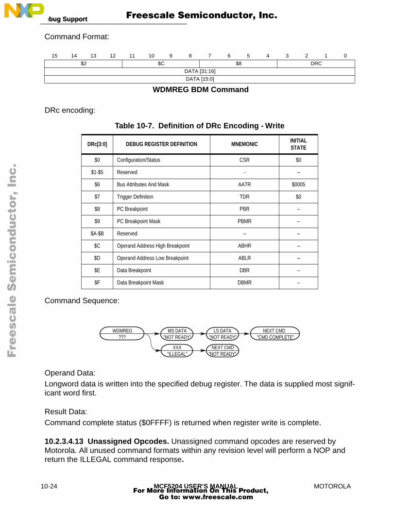
Debug SupportDebug Support
Fre
esc
ale
Se
mic
on
du
cto
r, I
Freescale Semiconductor, Inc.n
c..
.
Command Format:
DRc encoding:
Command Sequence:
Operand Data:Longword data is written into the specified debug register. The data is supplied most signif-icant word first.
Result Data:Command complete status ($0FFFF) is returned when register write is complete.
10.2.3.4.13 Unassigned Opcodes. Unassigned command opcodes are reserved by Motorola. All unused command formats within any revision level will perform a NOP and return the ILLEGAL command response.
15 14 13 12 11 10 9 8 7 6 5 4 3 2 1 0
$2 $C $8 DRC
DATA [31:16]
DATA [15:0]
WDMREG BDM Command
Table 10-7. Definition of DRc Encoding - Write
DRc[3:0] DEBUG REGISTER DEFINITION MNEMONICINITIAL STATE
$0 Configuration/Status CSR $0
$1-$5 Reserved - –
$6 Bus Attributes And Mask AATR $0005
$7 Trigger Definition TDR $0
$8 PC Breakpoint PBR –
$9 PC Breakpoint Mask PBMR –
$A-$B Reserved – –
$C Operand Address High Breakpoint ABHR –
$D Operand Address Low Breakpoint ABLR –
$E Data Breakpoint DBR –
$F Data Breakpoint Mask DBMR –
MS DATA"NOT READY"
XXX"ILLEGAL"
LS DATA"NOT READY"
NEXT CMD"NOT READY"
WDMREG???
NEXT CMD"CMD COMPLETE"
10-24 MCF5204 USER’S MANUAL MOTOROLA For More Information On This Product,
Go to: www.freescale.com

Debug Support
Fre
esc
ale
Se
mic
on
du
cto
r, I
Freescale Semiconductor, Inc.n
c..
.
10.3 REAL-TIME DEBUG SUPPORTColdFire processors provide support for the debug of real-time applications. For these types of embedded systems, the processor cannot be halted during debug, but must continue to operate. The foundation of this area of debug support is that while the processor cannot be halted to allow debugging, the system can tolerate small intrusions into the real-time operation.
As discussed in the previous section, the Debug module provides a number of hardware resources to support various hardware breakpoint functions. Specifically, three types of breakpoints are supported: PC with mask, operand address range, and data with mask. These three basic breakpoints can be configured into one- or two-level triggers with the exact trigger response also programmable.
10.3.1 Programming ModelIn addition to the existing BDM commands that provide access to the processor’s registers
and the memory subsystem, the Debug module contains a number of registers to support the required functionality. All of these registers are treated as 32-bit quantities, regardless of the actual number of bits in the implementation. The registers, known as the Debug Control Registers (DRc), are addressed using a 4-bit value as part of two new BDM commands (WDREG, RDREG).
These registers are also accessible from the processor’s supervisor programming model through the execution of the WDEBUG instruction (Figure 10-5 illustrates the Debug module programming model). Thus, the breakpoint hardware within the Debug module can be accessed by the external development system using the serial interface, or by the operating system running on the processor core. It is the responsibility of the software to guarantee that all accesses to these resources are serialized and logically consistent. The hardware
Figure 10-5. Debug Programming Model
ADDRESSBREAKPOINT REGISTERS
PC BREAKPOINTREGISTERS
DATA BREAKPOINTREGISTERS
ABLRABHR
PBRPBMR
DBMRDBR
TDR
15
0
31
TRIGGER DEFINITIONREGISTER
ADDRESS ATTRIBUTETRIGGER REGISTERAATR
7
0
15
CSRCONFIGURATION/STATUSREGISTER
MOTOROLA MCF5204 USER’S MANUAL 10-25 For More Information On This Product,
Go to: www.freescale.com

Debug SupportDebug Support
Fre
esc
ale
Se
mic
on
du
cto
r, I
Freescale Semiconductor, Inc.n
c..
.
provides a locking mechanism in the CSR to allow the external development system to disable any attempted writes by the processor to the Breakpoint Registers (setting IPW =1).
10.3.1.1 ADDRESS BREAKPOINT REGISTERS (ABLR, ABHR). The Address Breakpoint Registers define an upper (ABHR) and a lower (ABLR) boundary for a region in the operand logical address space of the processor that can be used as part of the trigger. The ABLR and ABHR values are compared with the ColdFire CPU core address signals, as defined by the setting of the TDR.
10.3.1.2 ADDRESS ATTRIBUTE BREAKPOINT REGISTER (AATR). The AATR defines the address attributes and a mask to be matched in the trigger. The AATR value is compared with the ColdFire CPU core address attribute signals, as defined by the setting of the TDR. The AATR is accessible in supervisor mode as debug control register $6 using the WDEBUG instruction and via the BDM port using the WDMREG command. The lower five bits of the AATR is also used for BDM command definition to define the address space for memory references as described in subsection 10.3.2.1 Reuse of Debug Module Hardware .
RM–Read/Write MaskThis field corresponds to the R-field. Setting this bit causes R to be ignored in address comparisons.
SZM–Size MaskThis field corresponds to the SZ field. Setting a bit in this field causes the corresponding bitin SZ to be ignored in address comparisons.
TTM–Transfer Type MaskThis field corresponds to the TT field. Setting a bit in this field causes the corresponding bitin TT to be ignored in address comparisons.
TMM–Transfer Modifier MaskThis field corresponds to the TM field. Setting a bit in this field causes the corresponding bitin TM to be ignored in address comparisons.
R–Read/WriteThis field is compared with the ColdFire CPU core R/W signal. A high level indicates a readcycle and a low level indicates a write cycle.
SZ–SizeThis field is compared with the ColdFire CPU core SIZ signals.
15 14 13 12 11 10 8 7 6 5 4 3 2 0
RM SZM TTM TMM R SZ TT TM
AATR Bit Definitions
10-26 MCF5204 USER’S MANUAL MOTOROLA For More Information On This Product,
Go to: www.freescale.com

Debug Support
Fre
esc
ale
Se
mic
on
du
cto
r, I
Freescale Semiconductor, Inc.n
c..
.
SZ—-SizeThis field is compared to the ColdFire CPU core SIZ signals. These signals indicate the datasize for the bus transfer. Table 10-8 shows the definitions for the SZ encodings.
TT–Transfer TypeThis field is compared with the ColdFire CPU core TT signals. These signals indicate thetransfer type for the bus transfer. Table 10-9 shows the definition of the TT encodings.
TM–Transfer ModifierThis field is compared with the ColdFire CPU core TM signals. These signals provide sup-plemental information for each transfer type. Table 10-10 shows encodings for normal trans-fers and Table 10-11 shows the encodings for alternate and debug access transfers. For
Table 10-8. SZ Encodings
SZ[1:0] TRANSFER SIZE
00 Longword (4 bytes)
01 Byte
10 Word (2 bytes)
11 Line (4 x 4 bytes)
Table 10-9. Transfer Type Encodings
TT[1:0] TRANSFER TYPE
00 Normal Access
01 Reserved
10 Alternate and Debug Access
11 Acknowledge Access
MOTOROLA MCF5204 USER’S MANUAL 10-27 For More Information On This Product,
Go to: www.freescale.com

Debug SupportDebug Support
Fre
esc
ale
Se
mic
on
du
cto
r, I
Freescale Semiconductor, Inc.n
c..
.
interrupt acknowledge transfers, the TM [2:0] signals indicate the interrupt level being acknowledged. For CPU space transfers initiated by a MOVEC instruction or a debutWCREG command, TT[1:0] = 11 and TM[2:0] = 000. For breakpoint-acknowledge transfers,the TM signals are low.
10.3.1.3 PROGRAM COUNTER BREAKPOINT REGISTER (PBR, PBMR). The PC Breakpoint Registers define a region in the instruction address space of the processor that can be used as part of the trigger. The PBR value is masked by the PBMR value, allowing only those bits in PBR that have a corresponding zero in PBMR to be compared with the processor’s program counter register, as defined in the TDR.
10.3.1.4 DATA BREAKPOINT REGISTER (DBR, DBMR). The Data Breakpoint Registers define a specific data pattern that can be used as part of the trigger into debug mode.The DBR value is masked by the DBMR value, allowing only those bits in DBR that have a corresponding zero in DBMR to be compared with the ColdFire CPU core data signals, as defined in the TDR.
Table 10-10. Transfer Modifier Encodings for Normal Transfers
TM[2:0] TRANSFER MODIFIER
000 Reserved
001 User Data Access
010 User Code Access
011 - 100 Reserved
101 Supervisor Data Access
110 Supervisor Code Access
111 Reserved
Table 10-11. Transfer Modifier Encodings for Alternate Access Transfers
TM[2:0] TRANSFER MODIFIER
000 - 100, 111 Reserved
101 Emulator Mode Data Access
110 Emulator Mode Code Access
10-28 MCF5204 USER’S MANUAL MOTOROLA For More Information On This Product,
Go to: www.freescale.com

Debug Support
Fre
esc
ale
Se
mic
on
du
cto
r, I
Freescale Semiconductor, Inc.n
c..
.
The data breakpoint register supports both aligned and misaligned operand references. The relationship between the processor core address, the access size, and the corresponding location within the 32-bit core data bus is shown in Table 10-12.
10.3.1.5 TRIGGER DEFINITION REGISTER (TDR). The TDR configures the operation of the hardware breakpoint logic within the Debug module and controls the actions taken under the defined conditions. The breakpoint logic may be configured as a one- or two-level trigger, where bits [29:16] of the TDR define the 2nd level trigger, bits [13:0] define the first level trigger, and bits [31:30] define the trigger response.
Reset clears the TDR.
TRC–Trigger Response ControlThe trigger response control determines how the processor is to respond to a completedtrigger condition. The trigger response is always displayed on the DDATA pins.
00=displayed on DDATA pins only01=processor halt10=debug interrupt11=reserved
EBL–Enable Breakpoint LevelIf set, this bit serves as the global enable for the breakpoint trigger. If cleared, all breakpointsare disabled.
Table 10-12. Core Address, Access Size, and Operand Location
CORE ADDRESS[1:0]
ACCESS SIZE
OPERAND LOCATION
00 Byte Data[31:24]
01 Byte Data[23:16]
10 Byte Data[15:08]
11 Byte Data[07:00]
0- Word Data[31:16]
1- Word Data[15:00]
-- Long Data[31:00]
31 30 29 28 27 26 25 24 23 22 21 20 19 18 17 16
TRC EBL EDLW EDWL EDWU EDLL EDLM EDUM EDUU DI EAI EAR EAL EPC PCI
15 14 13 12 11 10 9 8 7 6 5 4 3 2 1 0
00 EBL EDLW EDWL EDWU EDLL EDLM EDUM EDUU DI EAI EAR EAL EPC PCI
TDR Bit Definitions
MOTOROLA MCF5204 USER’S MANUAL 10-29 For More Information On This Product,
Go to: www.freescale.com
Debug SupportDebug Support
Fre
esc
ale
Se
mic
on
du
cto
r, I
Freescale Semiconductor, Inc.n
c..
.
EDLW–Enable Data Breakpoint for the Data LongwordIf set, this bit enables the data breakpoint based on the core data bus (KD) KD[31:0] longword. The assertion of any of the ED bits enables the data breakpoint. If all bits arecleared, the data breakpoint is disabled.
EDWL–Enable Data Breakpoint for the Lower Data WordIf set, this bit enables the data breakpoint based on the KD[15:0] word.
EDWU–Enable Data Breakpoint for the Upper Data WordIf set, this bit enables the data breakpoint trigger based on the KD[31:16] word.
EDLL–Enable Data Breakpoint for the Lower Lower Data ByteIf set, this bit enables the data breakpoint trigger based on the KD[7:0] byte.
EDLM–Enable Data Breakpoint for the Lower Middle Data ByteIf set, this bit enables the data breakpoint trigger based on the KD[15:8] byte.
EDUM–Enable Data Breakpoint for the Upper Middle Data ByteIf set, this bit enables the data breakpoint trigger based on the KD[23:16] byte.
EDUU–Enable Data Breakpoint for the Upper Upper Data ByteIf set, this bit enables the data breakpoint trigger based on the KD[31:24] byte.
DI–Data Breakpoint InvertThis bit provides a mechanism to invert the logical sense of all the data breakpoint comparators.This can develop a trigger based on the occurrence of a data value not equal to the one pro-grammed into the DBR.
The assertion of any of the EA bits enables the address breakpoint. If all three bits arecleared, this breakpoint is disabled.
EAI–Enable Address Breakpoint InvertedIf set, this bit enables the address breakpoint based outside the range defined by ABLR andABHR.
EAR–Enable Address Breakpoint RangeIf set, this bit enables the address breakpoint based on the inclusive range defined by ABLRand ABHR.
EAL–Enable Address Breakpoint LowIf set, this bit enables the address breakpoint based on the address contained in the ABLR.
EPC–Enable PC BreakpointIf set, this bit enables the PC breakpoint. Clearing this bit disables the PC breakpoint.
10-30 MCF5204 USER’S MANUAL MOTOROLA For More Information On This Product,
Go to: www.freescale.com

Debug Support
Fre
esc
ale
Se
mic
on
du
cto
r, I
Freescale Semiconductor, Inc.n
c..
.
PCI–PC Breakpoint InvertIf set, this bit allows execution outside a given region as defined by PBR and PBMR to en-able a trigger. If cleared, the PC breakpoint is defined within the region defined by PBR andPBMR.
10.3.1.6 CONFIGURATION/STATUS REGISTER (CSR). The Configuration/Status Register defines the operating configuration for the processor and memory subsystem. In addition to defining the microprocessor configuration, this register also contains status information from the breakpoint logic. The CSR is cleared during system reset. The CSR can
be read and written by the external development system and written by the supervisor programming model.
Status–Breakpoint StatusThis 4-bit field defines provides read-only status information concerning the hardwarebreakpoints. This field is defined as follows:
$0 = no breakpoints enabled$1 = waiting for level 1 breakpoint$2 = level 1 breakpoint triggered$5 = waiting for level 2 breakpoint$6 = level 2 breakpoint triggered
The CSR[30-28] bits are translated and output on the DDATA[3:1] signals where x is theDDATA[0] bit.
000x = no breakpoints enabled001x = waiting for level 1 breakpoint010x = level 1 breakpoint triggered101x = waiting for level 2 breakpoint110x = level 2 breakpoint triggered
This breakpoint status is also output on the DDATA port when the bus is not displaying Cold-Fire CPU core captured data. A write to the TDR resets this field.
FOF–Fault-on-FaultIf this read-only status bit is set, a catastrophic halt has occurred and forced entry into BDM.This bit is cleared on a read of the CSR.
31 28 27 26 25 24 23 17 16
STATUS FOF TRG HALT BKPT RESERVED IPW
15 14 13 12 11 10 9 8 7 6 5 4 3 2 1 0
MAP TRC EMU DDC UHE BTB 0 NPL IPI SSM 0 0 0 0
CSR Bit Definitions
MOTOROLA MCF5204 USER’S MANUAL 10-31 For More Information On This Product,
Go to: www.freescale.com

Debug SupportDebug Support
Fre
esc
ale
Se
mic
on
du
cto
r, I
Freescale Semiconductor, Inc.n
c..
.
TRG–Hardware Breakpoint TriggerIf this read-only status bit is set, a hardware breakpoint has halted the processor core andforced entry into BDM. This bit is cleared on a read from the CSR or when the processor isrestarted.
Halt–Processor HaltIf this read-only status bit is set, the processor has executed the HALT instruction and forcedentry into BDM. This bit is cleared on a read from the CSR or when the processor is restarted.
BKPT–BKPT AssertIf this read-only status bit is set, the BKPT signal was asserted, forcing the processor intoBDM. This bit is cleared on a read from the CSR or when the processor is restarted.
IPW–Inhibit Processor Writes to Debug RegistersIf set, this bit inhibits any processor-initiated writes to the Debug module’s programmingmodel registers. This bit can only be modified by commands from the external developmentsystem.
MAP–Force Processor References in Emulator ModeIf set, this bit forces the processor to map all references while in emulator mode to a specialaddress space, TT = 10, TM = 101 (data) and 110 (text). If cleared, all emulator-mode ref-erences are mapped into supervisor text and data spaces.
TRC–Force Emulation Mode on Trace ExceptionIf set, this bit forces the processor to enter emulator mode when a trace exception occurs.
EMU–Force Emulation ModeIf set, this bit forces the processor to begin execution in emulator mode. This bit is examinedonly when RSTI is negated, as the processor begins reset exception processing.
DDC–Debug Data ControlThis 2-bit field provides configuration control for capturing operand data for display on theDDATA port. The encodings are:
00 = no operand data is displayed01 = capture all M-Bus write data10 = capture all M-Bus read data11 = capture all M-Bus read and write data
In all cases, the DDATA port displays the number of bytes defined by the operand referencesize, i.e., byte displays 8 bits, word displays 16 bits, and long displays 32 bits.
UHE-User Halt EnableThis bit selects the CPU privilege level required to execute the HALT instruction.
0 = HALT is a privileged, supervisor-only instruction1 = HALT is a nonprivileged, supervisor/user instruction
10-32 MCF5204 USER’S MANUAL MOTOROLA For More Information On This Product,
Go to: www.freescale.com

Debug Support
Fre
esc
ale
Se
mic
on
du
cto
r, I
Freescale Semiconductor, Inc.n
c..
.
BTB–Branch Target BytesThis 2-bit field defines the number of bytes of branch target address to be displayed on theDDATA outputs. The encoding is
00 = 0 bytes01 = lower two bytes of the target address10 = lower three bytes of the target address11 = entire four-byte target address
The bytes are always displayed in a least-significant to most-significant order. The proces-sor captures only those target addresses associated with taken branches using a variant ad-dressing mode. This includes JMP and JSR instructions using address register indirect orindexed addressing modes, all RTE and RTS instructions as well as all exception vectors.
NPL–Nonpipelined ModeIf set, this bit forces the processor core to operate in a nonpipeline mode of operation. In thismode, the processor effectively executes a single instruction at a time with no overlap.
IPI–Ignore Pending InterruptsIf set, this bit forces the processor core to ignore any pending interrupt requests signalledon KIPL[2:0] while executing in single-instruction-step mode.
SSM–Single-Step ModeIf set, this bit forces the processor core to operate in a single-instruction-step mode. Whilein this mode, the processor executes a single instruction and then halts. While halted, anyof the BDM commands may be executed. On receipt of the GO command, the processorexecutes the next instruction and then halts again. This process continues until the single-instruction-step mode is disabled.
ReservedAll bits labeled Reserved or “0” are currently unused and reserved for future use.
10.3.2 Theory of OperationThe breakpoint hardware can be configured to respond to triggers in several ways. The preferred response is programmed into the Trigger Definition Register. In all situations where a breakpoint triggers, an indication is provided on the DDATA output port (when not displaying captured operands or branch addresses) as shown in Table 10-13.
MOTOROLA MCF5204 USER’S MANUAL 10-33 For More Information On This Product,
Go to: www.freescale.com

Debug SupportDebug Support
Fre
esc
ale
Se
mic
on
du
cto
r, I
Freescale Semiconductor, Inc.n
c..
.
The breakpoint status is also posted in the CSR.
The new BDM instructions load and configure the desired breakpoints using the appropriate registers. As the system operates, a breakpoint trigger generates a response as defined in the TDR. If the system can tolerate the processor being halted, a BDM-entry can be used. With the TRC bits of the TDR = 01, the breakpoint trigger causes the core to halt (as reflected in the PST = $F status). For PC breakpoints, the halt occurs before the targeted instruction is executed. For address and data breakpoints, the processor may have executed several additional instructions. For these breakpoints, trigger reporting is imprecise.
If the processor core cannot be halted, the special debug interrupt can be used. With this configuration, TRC bits of the TDR = 10, the breakpoint trigger is converted into a debug interrupt to the processor. This interrupt is treated as higher than the nonmaskable level 7 interrupt request. As with all interrupts, it is made pending the processor samples, once per instruction. Again, the hardware forces the PC breakpoint to occur immediately (before the execution of the targeted instruction). This is possible because the PC breakpoint comparison is enabled at the same time the interrupt sampling occurs. For the address and data breakpoints, the reporting is imprecise.
Once the debug interrupt is recognized, the processor aborts execution and initiates exception processing. At the initiation of the exception processing, the core enters emulator mode. Depending on the state of the MAP bit in the CSR, this mode may force all memory accesses (including the exception stack frame writes and the vector fetch) into a specially mapped address space signalled by TT = 2, TM = {5, 6}. After the standard 8-byte exception stack is created, the processor fetches a unique exception vector (offset $030) from the vector table.
Execution continues at the instruction address contained in this exception vector. All interrupts are ignored while in emulator mode. Users can program the debug-interrupt handler to perform the necessary context saves using the supervisor instruction set. As an
Table 10-13. DDATA, CSR[31:28] Breakpoint Response
DDATA[3:0], CSR[31:28]
BREAKPOINT STATUS
000x, $0 No breakpoints enabled
001x, $1 Waiting for Level 1 breakpoint
010x, $2 Level 1 breakpoint triggered
011x-100x, $3-4 Reserved
101x, $5 Waiting for Level 2 breakpoint
110x, $6 Level 2 breakpoint triggered
111x, $7-$F Reserved
10-34 MCF5204 USER’S MANUAL MOTOROLA For More Information On This Product,
Go to: www.freescale.com

Debug Support
Fre
esc
ale
Se
mic
on
du
cto
r, I
Freescale Semiconductor, Inc.n
c..
.
example, this handler may save the state of all the program-visible registers as well as the current context into a reserved memory area.
Once the required operations are completed, the return-from-exception (RTE) instruction is executed and the processor exits emulator mode. The processor status output port provides a unique encoding for emulator mode entry ($D) and exit ($7). Once the debug interrupt handler has completed its execution, the external development system can then access the reserved memory locations using the BDM commands to read memory.
10.3.2.1 REUSE OF DEBUG MODULE HARDWARE. The Debug module implementation provides a common hardware structure for both BDM and breakpoint functionality. Several structures are used for both BDM and breakpoint purposes. Table 10-14 identifies the shared hardware structures.
The shared use of these hardware structures means the loading of the register to perform any specified function is destructive to the shared function. For example, if an operand address breakpoint is loaded into the Debug module, a BDM command to access memory overwrites the breakpoint. If a data breakpoint is configured, a BDM write command overwrites the breakpoint contents.
10.3.3 Concurrent BDM and Processor OperationThe Debug module supports concurrent operation of both the processor and most BDM commands. BDM commands may be executed while the processor is running, except for the operations that access processor/memory registers:
• Read/Write Address and Data Registers
• Read/Write Control Registers
For BDM commands that access memory, the Debug module requests the ColdFire core’s bus. The processor responds by stalling the instruction fetch pipeline and then waiting until all current core bus activity is complete. At that time, the processor relinquishes the core bus to allow the Debug module to perform the required operation. After the conclusion of the Debug module core bus cycle, the processor reclaims ownership of the core bus.
The development system must use caution in configuring the Breakpoint Registers if the processor is executing. The Debug module does not contain any hardware interlocks, so Motorola recommends that the TDR be disabled while the Breakpoint Registers are being loaded. At the conclusion of this process, the TDR can be written to define the exact trigger. This approach guarantees that no spurious breakpoint triggers will occur.
Table 10-14. Shared BDM/Breakpoint Hardware
REGISTER BDM FUNCTION BREAKPOINT FUNCTION
AATR Bus attributes for all memory commands Attributes for address breakpoint
ABHR Address for all memory commands Address for address breakpoint
DBR Data for all BDM write commands Data for data breakpoint
MOTOROLA MCF5204 USER’S MANUAL 10-35 For More Information On This Product,
Go to: www.freescale.com

Debug SupportDebug Support
Fre
esc
ale
Se
mic
on
du
cto
r, I
Freescale Semiconductor, Inc.n
c..
.
Because there are no hardware interlocks in the debug unit, no BDM operations are allowed while the CPU is writing the debug’s registers (SDSCLK must be inactive).
10.4 MOTOROLA RECOMMENDED BDM PINOUTThe ColdFire BDM connector is a 26-pin Berg Connector arranged 2x13, shown below in Figure 10-6.
NOTES:1 Supplied by target2 Pins reserved for BDM developer use. Contact developer.* Denotes a vectored signal
Figure 10-6. 26-pin Berg Connector Arranged 2x13
10.4.1 Differences Between the ColdFire BDM and a CPU32 BDM1. DSCLK, BKPT, and DSDI need to meet the setup and hold times relative to the rising
edge of the processor clock to prevent the processor from propagating metastable states.
2. DSO transitions relative to the rising edge of DSCLK only. In the CPU32 BDM, DSO transitions between serial transfers to indicate to the development system that a com-mand has successfully completed. The ColdFire BDM does not support this feature.
1
3
5
7
9
11
13
15
17
19
21
23
25
2
4
6
8
10
12
14
16
18
20
22
24
26
DEVELOPER RESERVED2
GND
GND
RESET*
+5V1
GND
PST2
PST0
DDATA2
DDATA0*
MOTOROLA RESERVED
GND
VCC_CPU
BKPT
DSCLK
DEVELOPER RESERVED2
DSI
DSO
PST3*
PST1
DDATA3*
DDATA1
GND
MOTOROLA RESERVED
CLK_CPU
TEA
10-36 MCF5204 USER’S MANUAL MOTOROLA For More Information On This Product,
Go to: www.freescale.com

Debug SupportDebug Support
Fre
esc
ale
Se
mic
on
du
cto
r, I
Freescale Semiconductor, Inc.n
c..
.
3. The development system must note that the DSO is not valid during the first rising edge of DSCLK. Instead, the first rising edge of DSCLK causes DSO to transmit the MSB of DSO. A serial transfer is illustrated in Figure 10-7.
Figure 10-7. Serial Transfer Illustration
16 15 0
16 15 1 0
DSCLK
DSI
DSO
10-37 MCF5204 USER’S MANUAL MOTOROLA For More Information On This Product,
Go to: www.freescale.com
Date: 08-21-98
Revision No: 0.1
Pages affected: See change bars
F
ree
sca
le S
em
ico
nd
uc
tor,
I
Freescale Semiconductor, Inc.n
c..
.
SECTION 11 JTAG SPECIFICATION
11.1 IEEE 1149.1 STANDARD (JTAG) SPECIFICATION
The MCF5204 processors include dedicated user-accessible test logic that is fully compliant with the IEEE standard 1149.1 test access port and boundary-scan architecture. The following description should be used in conjunction with the supporting IEEE document listed above. This section includes the description of those chip-specific items that the IEEE standard requires as well as those items specific to the MCF5204 implementation.
The MCF5204 JTAG test architecture implementation currently supports circuit board test strategies that are based on the IEEE standard. This architecture provides access to all of the data and chip control pins from the board edge connector through the standard four-pin test access port (TAP) and the active-low JTAG reset pin, TRST. The test logic itself uses a static design and is wholly independent of the system logic, except where the JTAG is subordinate to other complimentary test modes (used for manufacturing test support). When in subordinate mode, the JTAG test logic is placed in reset and the TAP pins can be used for other purposes in accordance with the rules and restrictions set forth using a JTAG compliance-enable pin.
The MCF5204 JTAG implementation can
• Perform boundary-scan operations to test circuit board electrical continuity
• Bypass the MCF5204 device by reducing the shift register path to a single cell
• Sample the MCF5204 system pins during operation and transparently shift out the result
• Set the MCF5204 output drive pins to fixed logic values while reducing the shift register path to a single cell
• Protect the MCF5204 system output and input pins from backdriving and random toggling (such as during in-circuit testing) by placing all system signal pins to high impedance
MOTOROLA MCF5204 USER’S MANUAL 11-1 For More Information On This Product,
Go to: www.freescale.com

JTAG Specification
F
ree
sca
le S
em
ico
nd
uc
tor,
I
Freescale Semiconductor, Inc.n
c..
.
The IEEE Standard 1149.1 test logic cannot be considered completely benign to those planning not to use JTAG capability. Customers must observe certain precautions to ensure that this logic does not interfere with system or debug operation.
Figure 11-1. JTAG MODE, JTAG Disabled
Figure 11-1 shows pin logical values recommended for disabling JTAG with the part in JTAG mode.
While in JTAG mode, input pins TDI / DSI, TMS / BKPT, and TRST / DSCLK have internal pullups enabled. Figure 11-2 shows pin logical values recommended for disabling JTAG with the part in Background Debug mode.
Figure 11-2. Background Debug Mode, JTAG Disabled
11.2 OVERVIEWFigure 11-3 illustrates the block diagram or programmer’s model of the MCF5204 implementation of the 1149.1 IEEE Standard. The test logic includes several test data registers, an instruction register, instruction register control decode, and a 16-state dedicated TAP controller (defined in Figure 11-4).
MTMOD
TDI / DSI
TMS / BKPT
TCK
TRST / DSCLK
HIZ
LOGIC 0
LOGIC 1
SYSTEM RST
LOGIC 0
RST
NC
NC
MTMOD
TDI /DSI
TMS / BKPT
TCK
TRST / DSCLK
HIZ
LOGIC 1
LOGIC 1
BDM INTERFACE
LOGIC 0
11-2 MCF5204 USER’S MANUAL MOTOROLA For More Information On This Product,
Go to: www.freescale.com
JTAG Specification
F
ree
sca
le S
em
ico
nd
uc
tor,
I
Freescale Semiconductor, Inc.n
c..
.
11.2.1 JTAG Pin DescriptionsMTMOD is defined to be a compliance-enable input per Section 3.8 of the IEEE Standard 1149.1a-1993 entitled “Subordination of this Standard within a Higher Level Test Strategy.”
Given the compliance-enable state described above, the pin descriptions apply in Table 11-1.
MOTOROLA MCF5204 USER’S MANUAL 11-3 For More Information On This Product,
Go to: www.freescale.com

JTAG Specification
F
ree
sca
le S
em
ico
nd
uc
tor,
I
Freescale Semiconductor, Inc.n
c..
.
Table 11-1. JTAG Pin Description
Figure 11-3. JTAG Test Logic Block Diagram
PIN DESCRIPTION
TCK A test clock input that synchronizes test logic operations
TMS A test mode select input with a default internal pullup resistor that is sampled on the rising edge of TCK to sequence the TAP controller
TDI A serial test data input with a default internal pullup resistor that is sampled on the rising edge of T
TDO A three-state test data output that is actively driven only in the Shift-IR and Shift-DR controller states and only updates on the falling edge of TCK
TRST An active-low asynchronous reset with a default internal pullup resistor that forces the TAP controller into the test-logic-reset state.
BOUNDARY SCAN REGISTER
BYPASS
MUX
3-BIT INSTRUCTION DECODE
3-BIT INSTRUCTION REGISTER
MUX
TAPCONTROLLER
TEST DATA REGISTERS
TDI
TMS
TCK
TRST
TDO
V+
V+
V+
11-4 MCF5204 USER’S MANUAL MOTOROLA For More Information On This Product,
Go to: www.freescale.com

JTAG Specification
F
ree
sca
le S
em
ico
nd
uc
tor,
I
Freescale Semiconductor, Inc.n
c..
.
11.3 JTAG REGISTER DESCRIPTION
11.3.1 JTAG Instruction Shift RegisterThe MCF5204 IEEE 1149.1 Standard implementation uses a 3-bit instruction-shift register without parity. This register transfers its value to a parallel hold register and applies one of eight possible instructions on the falling edge of TCK when the TAP state machine is in the update-IR state. The instructions can be loaded into the shift portion of the register by placing the serial data on the TDI pin prior to each rising edge of TCK. The MSB of the instruction shift register is the bit closest to the TDI pin and the LSB is the bit closest to the TDO pin.
Table 11-2 lists the public customer-usable instructions that are supported along with their encoding.
The IEEE 1149.1 Standard requires the EXTEST, SAMPLE/PRELOAD, and BYPASS instructions. CLAMP and HIGHZ are optional standard instructions that are supported by the MCF5204 implementation and are described in the 1149.1.
11.3.1.1 EXTEST INSTRUCTION. The external test instruction (EXTEST) selects the boundary scan register. The EXTEST instruction forces all output pins and bidirectional pins configured as outputs to the preloaded fixed values (with the SAMPLE/PRELOAD instruction) and held in the boundary scan update registers. The EXTEST instruction can also configure the direction of bidirectional pins and establish high-impedance states on some pins. The EXTEST instruction becomes active on the falling edge of TCK in the update-IR state when the data held in the instruction-shift register is equivalent to octal 0.
11.3.1.2 SAMPLE/PRELOAD INSTRUCTION. The SAMPLE/PRELOAD instruction provides two separate functions. First, it obtains a sample of the system data and control signals present at the MCF5204 input pins and just prior to the boundary scan cell at the output pins. This sampling occurs on the rising edge of TCK in the capture-DR state when an instruction encoding of octal 4 is resident in the instruction register. Customers can observe this sampled data by shifting it through the boundary-scan register to the output TDO by using the shift-DR state. Both the data capture and the shift operation are transparent to system operation. Customers are responsible for providing some form of
Table 11-2. JTAG Instructions
INSTRUCTION ABBR CLASS IR[2:0] INSTRUCTION SUMMARY
EXTEST EXT Required 000 Select BS register while applying fixed values to output pins and asserting functional reset
SAMPLE/PRELOAD
SMP Required 100 Selects BS register for shift, sample, and preload without disturbing functional operation
HIGHZ HIZ Optional 101 Selects the bypass register while three-stating all output pins and asserting functional reset
CLAMP CMP Optional 110 Selects bypass while applying fixed values to output pins and asserting functional reset
BYPASS BYP Required 111 Selects the bypass register for data operations
MOTOROLA MCF5204 USER’S MANUAL 11-5 For More Information On This Product,
Go to: www.freescale.com

JTAG Specification
F
ree
sca
le S
em
ico
nd
uc
tor,
I
Freescale Semiconductor, Inc.n
c..
.
external synchronization to achieve meaningful results because there is no internal synchronization between TCK and the system clock, CLK.
The second function of the SAMPLE/PRELOAD instruction is to initialize the boundary scan register update cells before selecting EXTEST or CLAMP. This is achieved by ignoring the data being shifted out of the TDO pin while shifting in initialization data. The update-DR state in conjunction with the falling edge of TCK can then transfer this data to the update cells. This data will be applied to the external output pins when one of the instructions listed above is applied.
11.3.1.3 HIGHZ INSTRUCTION. The HIGHZ instruction anticipates the need to backdrive the output pins and protect the input pins from random toggling during circuit board testing. The HIGHZ instruction selects the bypass register, forcing all output and bidirectional pins to the high-impedance state.
The HIGHZ instruction goes active on the falling edge of TCK in the update-IR state when the data held in the instruction shift register is equivalent to octal 5.
11.3.1.4 CLAMP INSTRUCTION. The CLAMP instruction selects the bypass register and asserts functional reset while simultaneously forcing all output pins and bidirectional pins configured as outputs to the fixed values that are preloaded and held in the boundary scan update registers. This instruction enhances test efficiency by reducing the overall shift path to a single bit (the bypass register) while conducting an EXTEST type of instruction through the boundary-scan register.
The CLAMP instruction becomes active on the falling edge of TCK in the update-IR state when the data held in the instruction-shift register is equivalent to octal 6.
11.3.1.5 BYPASS INSTRUCTION. The BYPASS instruction selects the single-bit bypass register, creating a single-bit shift register path from the TDI pin to the bypass register to the TDO pin. This instruction enhances test efficiency by reducing the overall shift path when a device other than the MCF5204 processor becomes the device under test on a board design with multiple chips on the overall 1149.1 defined boundary-scan chain. The bypass register has been implemented in accordance with 1149.1 so that the shift register stage is set to logic zero on the rising edge of TCK following entry into the capture-DR state. Therefore, the first bit to be shifted out after selecting the bypass register is always a logic zero (this is to differentiate a part that supports an IDCODE register from a part that supports only the bypass register). The BYPASS instruction goes active on the falling edge of TCK in the update-IR state when the data held in the instruction shift register is equivalent to a octal 7.
11.3.2 JTAG BOUNDARY-SCAN REGISTERAn IEEE 1149.1-compliant boundary-scan register has been included on the MCF5204 model. Customers can connect this boundary-scan register between TDI and TDO when the EXTEST or SAMPLE/PRELOAD instructions are selected. This register captures signal pin data on the input pins, forces fixed values on the output signal pins, and selects the direction and drive characteristics (a logic value or high impedance) of the bidirectional and three-state signal pins.
11-6 MCF5204 USER’S MANUAL MOTOROLA For More Information On This Product,
Go to: www.freescale.com

JTAG Specification
F
ree
sca
le S
em
ico
nd
uc
tor,
I
Freescale Semiconductor, Inc.n
c..
.
11.4 TAP CONTROLLERThe current state of the TAP controller is determined by the value of TMS at the rising edge of TCK. There are basically two paths that the TAP controller can follow: The first, for executing JTAG instructions, and the second, for manipulating JTAG data based on the JTAG instructions. The various states of the TAP controller are shown in the diagram below. For more detail on each state, refer to the IEEE 1149.1 Standard JTAG document. Do note, though, that from any state the TAP controller is in, Test-Logic-Reset can be entered if TMS is held high for at least five rising edges of TCK.
MOTOROLA MCF5204 USER’S MANUAL 11-7 For More Information On This Product,
Go to: www.freescale.com

JTAG Specification
F
ree
sca
le S
em
ico
nd
uc
tor,
I
Freescale Semiconductor, Inc.n
c..
.
Figure 11-4. JTAG TAP Controller State Machine
11.4.1 JTAG BYPASS REGISTERThe MCF5204 includes an IEEE 1149.1-compliant bypass register, which creates a single bit shift register path from TDI to the bypass register to TDO when the BYPASS instruction is selected.
TEST - LOGIC - RESET
TLR
RUN - TEST - IDLE
RTI
SELECT - DR - SCAN
SeDR
CAPTURE - IR
UPDATE - IR
EXIT2 - IR
PAUSE - IR
EXIT1 - IR
SHIFT - IR
CAPTURE - DR
UPDATE - DR
Exit2 - DR
PAUSE - DR
EXIT1 - DR
SHIFT - DR
0
0
0
1
0
1
1
0
0
0
1
0
1
1
0
1 11
1 1
0
0
0
0
1 1
1 1
0 0
0
1
CaDR
ShDR
E1DR
PaDR
E2DR
UpDR
CaIR
ShIR
E1IR
PaIR
E2IR
UpIR
<-- VALUE OF TMS AT RISING EDGE OF TCK
SELECT - IR - SCANSeIR
1
11-8 MCF5204 USER’S MANUAL MOTOROLA For More Information On This Product,
Go to: www.freescale.com

JTAG Specification
F
ree
sca
le S
em
ico
nd
uc
tor,
I
Freescale Semiconductor, Inc.n
c..
.
The 16 controller states are defined in detail in the IEEE 1149.1 standard.
For more information on the MCF5204, visit the following Internet address:
http://www.motorola.com/coldfire
The IEEE 1149 Standard JTAG specification is available directly from IEEE:
IEEE Standards Department
445 Hoes Lane
P.O. Box 1331
Piscataway, NJ 08855-1331
USA
http://stdsbbs.ieee.org/
Fax: 908-981-9667
Information: 908-981-0060 or 1-800-678-4333
MOTOROLA MCF5204 USER’S MANUAL 11-9 For More Information On This Product,
Go to: www.freescale.com

MOTOROLA
MCF5204 USERÕS MANUAL
12-1
SECTION 12ELECTRICAL CHARACTERISTICS
12.1 MAXIMUM RATINGS
The ratings in the above table deÞne maximum conditions under which the MCF5204 device will operate
without being damaged.
This device contains circuitry that protects against damage from high static voltages or electrical Þelds; however, users should take normal precautions to avoid application of any voltages higher than maximum-rated voltages to this high-impedance circuit. Operational reliability improves when unused inputs are tied to an appropriate logic voltage level (e.g., either GND or V
CC
).
a
This published maximum operating ambient temperature should be used only as a system design guideline. All device operating parameters are guaranteed only when the junction temperature lies within the speciÞed range.
NOTE
At press time power dissipation Þgures were not available. Refer to the World Wide Web site at http://www.mot.com/ColdFire for the latest accurate power dissipation
information for the MCF5204 processor.
RATING SYMBOL VALUE UNIT
Supply voltage V
CC
-0.3 to +7.0 V
Input voltage V
in
-0.5 to V
CC
+ 0.5V V
Storage temperature range T
stg
-55 to 150
o
C
CHARACTERISTIC SYMBOL VALUE UNIT
Maximum operating junction temperature T
J
TBD
o
C
Maximum operating ambient temperature - 70
a o
C
Minimum operating ambient temperature T
A
0
o
C
DATE: 08-21-98
REVISION NO: 0.1
PAGES AFFECTED: SEE CHANGE BARS
Fre
esc
ale
Se
mic
on
du
cto
r, I
Freescale Semiconductor, Inc.
For More Information On This Product, Go to: www.freescale.com
nc
...

Electrical Characteristics
12-2
MCF5204 USERÕS MANUAL
MOTOROLA
.
12.2 CLOCK INPUT SPECIFICATION
Figure 12-1. Clock Input Timing
* SpeciÞcation values not tested
CHARACTERISTIC SYMBOL
b
VALUE RATING
Thermal resistance, junction to ambientThermal resistance, junction to top reference
q
ja
Y
jt
532.7
o
C/W
o
C/W
b
q
ja
and
Y
jt
parameters are measured in accordance with EIA/JEDEC Standard 51-2 for natural convection.
Motorola recommends the use of
q
ja
and power dissipation speciÞcations in the system design to prevent device junction temperatures from exceeding the rated speciÞcation. System designers should be aware that device junc-tion temperatures can be signiÞcantly inßuenced by the board layout and surrounding devices. Conformance to the device junction temperature speciÞcation can be veriÞed by physical measurement in the customersÕ system using the
Y
jt
parameter, the device power dissipation, and the method described in EIA/JEDEC Standard 51-2.
NUM CHARACTERISTIC16.67 MHz 25 MHz
33 MHzUNIT
MIN MAX MIN MAX MIN MAX
C1 CLK cycle time 60 Ñ 40 Ñ 30 Ñ ns
C2* CLK rise time Ñ 5 Ñ 5 Ñ 5 ns
C3
*
CLK fall time Ñ 5 Ñ 5 Ñ 5 ns
C4 CLK duty cycle measured at 1.5 V 40 60 40 60 40 60 %
C4a CLK pulse width high measured at 1.5 V 24 36 16 24 12 18 ns
C4b CLK pulse width low measured at 1.5 V 24 36 16 24 12 18 ns
C1
C4a C4b
VIL
VIH
C2C3
Fre
esc
ale
Se
mic
on
du
cto
r, I
Freescale Semiconductor, Inc.
For More Information On This Product, Go to: www.freescale.com
nc
...

Electrical Characteristics
MOTOROLA
MCF5204 USERÕS MANUAL
12-3
12.3
DC ELECTRICAL SPECIFICATIONS
12.4 AC ELECTRICAL SPECIFICATION
12.4.1 Maximum Output Loading
12.4.2 Bus Timing
* This speciÞcation periodically sampled but not 100% tested.
CHARACTERISTIC SYMBOL MIN MAX UNIT
Operation Voltage Range VCC 4.75 5.25 VInput high voltage V
IH
2 VCC V
Input low voltage V
IL
GND 0.8 V
Input leakage current @ GND, V
CC
I
in
Ñ 20
m
A
HI-Z (three-state) leakage current @ GND, V
CC
I
TSI
Ñ 20
m
A
Output high voltage, I
OH
= 5 mA V
OH
2.4 Ñ V
Output low voltage, I
OL
= 5 mA V
OL
Ñ 0.5 V
Pin capacitance* C
in
Ñ 10 pF
CHARACTERISTICS SYMBOL MAXIMUM UNIT
Load Capacitance(A[21:0],D[15:0],UWE,LWE,WE,RE,PP[1:0])
C
L
75 pF
Load Capacitance(CSx, TXD, RTS, TDO, TOUT, ATS(BUSW), PP[7:2](TIN,TOUT,RXD,TXD,CTS,RTS), PST[3:0], DDATA[3:0])
C
L
50 pF
16.67 MHZ 25 MHZ 33.33 MHZ
NUM NAME INPUT CHARACTERISTICS MIN MAX MIN MAX MIN MAX UNITS
B1 tAIST Asynchronous
1
Input Setup Time 12 10 8 ns
B1a tAIPW Asynchronous
1
Input Pulse Width (minimum) 1 1 1 clk
B2 tAIHT Asynchronous Input Hold Time 5 4 3 nsB3 tDICH Data In to Clock High (setup) 10 5 5 nsB4 tCHDI Clock High to Data in Invalid (hold) 5 4 3 ns
B5 tCHDIZ Clock High to Data in HIZ
3
5 4 3 ns
Fre
esc
ale
Se
mic
on
du
cto
r, I
Freescale Semiconductor, Inc.
For More Information On This Product, Go to: www.freescale.com
nc
...

Electrical Characteristics
12-4
MCF5204 USERÕS MANUAL
MOTOROLA
*Output timing is measured at pin. Timings are specified to the 1.5V crossing.
1
Asynchronous inputs - IRQ[3:0], DTACK, RESET, BKPT, BUSW
2
Strobes refer to all Chip Selects and Bus Strobes including CSx, WE, RE, UWE(UDS), LWE(LDS)
3
SpeciÞcation guaranteed by design. Spec not tested, but periodically sampled and veriÞed.
12.4.2.1 . INPUT SETUP AND HOLD WAVEFORM
16.67 MHZ 25 MHZ 33.33 MHZ
NUM NAME OUTPUT CHARACTERISTIC* MIN MAX MIN MAX MIN MAX UNITS
B6 tCHAV Clock High to Address Valid 30 25 20 nsB7 tCHAZn Clock High to Address Invalid (hold) 3 3 3 nsB8 tCHDV Clock High to Data out Valid 30 25 20 nsB9 tCHDZ Clock High to Data out High Impedance 30 25 20 nsB10 tDOCH Data Out hold from Clock High (hold) 3 3 3 ns
B11 tCLSV Clock Low to Strobes
2
Valid CSx, WE,RE, UWE(UDS),LWE(LDS)
5 30 5 25 5 20 ns
B12 tCLSI Clock Low to Strobes Invalid (hold) 3 3 3 nsB13 tCHCV Clock High to ATS, PST, DDATA,DSOValid 30 25 20 nsB14 tCHCI Clock High to ATS, PST, DDATA, DSO Invalid (hold) 3 3 3 ns
B15 tAVSV
3
time Address Valid to Strobes
2
Valid 3 3 3 ns
1.5V1.5V1.5V
VALID
tHT
1.5V1.5V
CLK
INPUTS
tST
tPW
Fre
esc
ale
Se
mic
on
du
cto
r, I
Freescale Semiconductor, Inc.
For More Information On This Product, Go to: www.freescale.com
nc
...
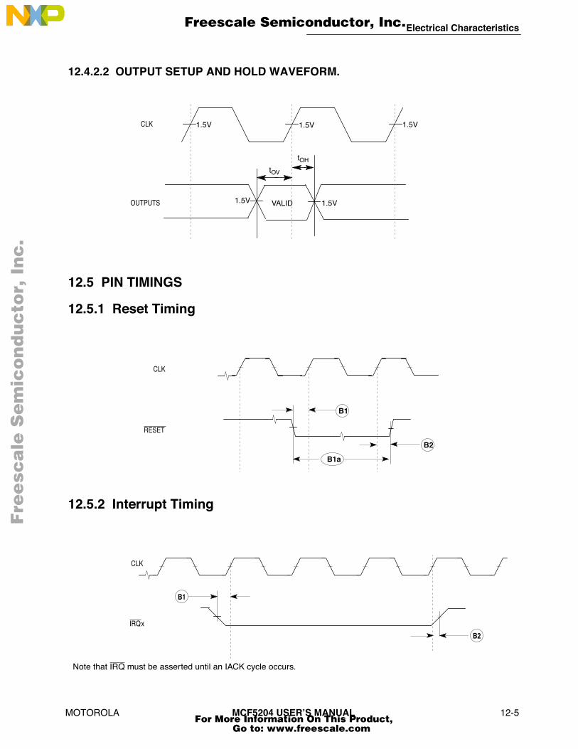
Electrical Characteristics
MOTOROLA
MCF5204 USERÕS MANUAL
12-5
12.4.2.2 OUTPUT SETUP AND HOLD WAVEFORM.
12.5 PIN TIMINGS
12.5.1 Reset Timing
12.5.2 Interrupt Timing
1.5V1.5V1.5V
VALID
tOH
1.5V1.5V
CLK
OUTPUTS
tOV
CLK
RESET
B2
B1
B1a
B1
B2
IRQx
CLK
Note that IRQ must be asserted until an IACK cycle occurs.
Fre
esc
ale
Se
mic
on
du
cto
r, I
Freescale Semiconductor, Inc.
For More Information On This Product, Go to: www.freescale.com
nc
...

Electrical Characteristics
12-6
MCF5204 USERÕS MANUAL
MOTOROLA
12.5.2.1 RESET CONFIGURATION TIMING.
Customers can configure the BUSW/ATS pin function at reset. The primary function of BUSW (boot ROM bus width) is always sampled at the negation of RESET. The alternate function of address transition start (ATS) can be activated by assertion of IRQ0 to a logic zero during reset. If activated, the ATS function will begin to drive out on the second clock after the negation of RESET.
In the case of an internal soft reset, the configuration of ATS and BUSW is not re-initialized.
12.5.3 Activation of ATS
RESET
CLK
IRQ0
B1
B1
B2
IRQ0 ISREGISTERED ON THERISING CLK EDGEPRECEDING RESET NEGATION
ATS(BUSW)
B13
B1
IRQ0 MAY REQUEST INTERRUPT
Fre
esc
ale
Se
mic
on
du
cto
r, I
Freescale Semiconductor, Inc.
For More Information On This Product, Go to: www.freescale.com
nc
...

Electrical Characteristics
MOTOROLA
MCF5204 USERÕS MANUAL
12-7
12.5.4 BUSW Timing Diagram
RESET
CLK
IRQ0
B1
B1
B2
IRQ0 ISREGISTERED ON THERISING CLK EDGEPRECEDING RESET NEGATION
BUSW(A TS)
B1
BUSW DRIVEN TO INDICATE BOOT ROM SIZE
IRQ0 MAY REQUEST INTERRUPT
B1
B2
Fre
esc
ale
Se
mic
on
du
cto
r, I
Freescale Semiconductor, Inc.
For More Information On This Product, Go to: www.freescale.com
nc
...

Electrical Characteristics
12-8
MCF5204 USERÕS MANUAL
MOTOROLA
12.6 BUS TIMING DIAGRAMS
Figure 12-2. Write Cycle Timing (shown with one wait state)
ATS
ADDR
CSx
RE
WE
DATA
DTACK
CLK
UWE /UDS
LWE /LDS
B8 B9
B10
B1
B11
B6
B7
B13
B2
B12
B14
B15
Fre
esc
ale
Se
mic
on
du
cto
r, I
Freescale Semiconductor, Inc.
For More Information On This Product, Go to: www.freescale.com
nc
...

Electrical Characteristics
MOTOROLA
MCF5204 USERÕS MANUAL
12-9
Figure 12-3. Read Cycle Timing Diagram (shown with one wait state inserted)
ATS
ADDR
CSx
RE
WE
DATA
DTACK
CLK
UWE /UDS
LWE /LDS
B13
B6
B3
B5
B7
B4
B1 B2
B14
B11
B12B15
Fre
esc
ale
Se
mic
on
du
cto
r, I
Freescale Semiconductor, Inc.
For More Information On This Product, Go to: www.freescale.com
nc
...

Electrical Characteristics
12-10
MCF5204 USERÕS MANUAL
MOTOROLA
12.6.1 AC Debug Timing Specification
12.6.1.1 DEBUG TIMING DIAGRAMS.
NUM NAME CHARACTERISTIC16.67 MHZ 25 MHZ 33.33 MHZ
UNITMIN MAX MIN MAX MIN MAX
B13/D1 tCHCV CLK to PST[3:0], DDATA[3:0], DSO Valid 30 25 20 ns
B14/D2 tCHCI CLK to PST[3:0],DDATA[3:0],DSO Invalid (hold) 3 3 3 ns
B1/D3 tAIST BKPT,DSCLK, DSI Valid to CLK (Setup) 12 10 8 ns
B2/D4 tAIHT CLK to BKPT, DSI Invalid (Hold) 5 4 3 ns
D1
D2
PST[3:0]
CLK
D1
D2
DSO
D4
DSI
D3
D1
D2
DDATA[3:0]
BKPT
D4
D3
DSCLK
D3
D3
Fre
esc
ale
Se
mic
on
du
cto
r, I
Freescale Semiconductor, Inc.
For More Information On This Product, Go to: www.freescale.com
nc
...

Electrical Characteristics
MOTOROLA
MCF5204 USERÕS MANUAL
12-11
12.6.2 HIZ Timing Specification
12.6.2.1 HIZ TIMING DIAGRAMS.
NUM NAME CHARACTERISTIC16.67 MHZ 25 MHZ 33.33 MHZ
UNITMIN MAX MIN MAX MIN MAX
H1 tHIZTS HIZ assert to three-state 60 60 60 ns
H2 tHIZD HIZ negate to driven 60 60 60 ns
HIZ
ALL
OUTPUTS
H1 H2
MTMOD = Ò0Ó
Fre
esc
ale
Se
mic
on
du
cto
r, I
Freescale Semiconductor, Inc.
For More Information On This Product, Go to: www.freescale.com
nc
...
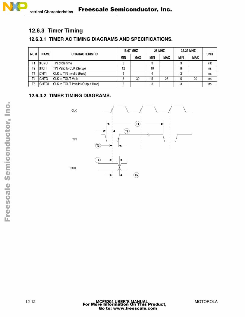
Electrical Characteristics
12-12 MCF5204 USERÕS MANUAL MOTOROLA
12.6.3 Timer Timing12.6.3.1 TIMER AC TIMING DIAGRAMS AND SPECIFICATIONS.
12.6.3.2 TIMER TIMING DIAGRAMS.
NUM NAME CHARACTERISTIC16.67 MHZ 25 MHZ 33.33 MHZ
UNITMIN MAX MIN MAX MIN MAX
T1 tTCYC TIN cycle time 3 3 3 clkT2 tTICH TIN Valid to CLK (Setup) 12 10 8 nsT3 tCHTII CLK to TIN Invalid (Hold) 5 4 3 nsT4 tCHTO CLK to TOUT Valid 5 30 5 25 5 20 nsT5 tCHTOI CLK to TOUT Invalid (Output Hold) 3 3 3 ns
TIN
T3
T2
CLK
T4
TOUT
T5
T1
Fre
esc
ale
Se
mic
on
du
cto
r, I
Freescale Semiconductor, Inc.
For More Information On This Product, Go to: www.freescale.com
nc
...

Electrical Characteristics
MOTOROLA MCF5204 USERÕS MANUAL 12-13
12.6.4 UART Timing12.6.4.1 UART MODULE AC TIMING SPECIFICATIONS.
12.6.4.2 UART TIMING DIAGRAMS.
NUM NAME CHARACTERISTIC16.67 MHZ 25 MHZ 33.33 MHZ
UNITMIN MAX MIN MAX MIN MAX
U1 tRXDICH RxD Valid to CLK (Setup) 12 10 8 nsU2 tCHRI CLK to RxD Invalid (Hold) 5 4 3 nsU3 tCTSICH CTS Valid to CLK (Setup) 12 10 8 nsU4 tCHCTSI CLK to CTS Invalid (Hold) 5 4 3 nsU5 tCHTXDV CLK to TxD Valid 5 30 5 25 5 20 nsU6 tCHTXDI CLK to TxD Invalid (Output Hold) 3 3 3 nsU7 tCHRTSV CLK to RTS Valid 5 30 5 25 5 20 nsU8 tCHRTSI CLK to RTS Invalid (Output Hold) 3 3 3 ns
U5
CLK
TxD out
U6
U1
U2
RxD in
U7
RTS out
U8
U3
U4
CTS in
Fre
esc
ale
Se
mic
on
du
cto
r, I
Freescale Semiconductor, Inc.
For More Information On This Product, Go to: www.freescale.com
nc
...

Electrical Characteristics
12-14 MCF5204 USERÕS MANUAL MOTOROLA
12.6.5 General-Purpose I/O Timing12.6.5.1 GENERAL-PURPOSE I/O AC TIMING SPECIFICATIONS.
General-purpose pin timing is determined by the primary function of the pin that the parallel port bit is multiplexed onto, if that timing has previously been defined. Otherwise, the timing specification in the previous table applies. Note that the timing from the previous table should match with the timing of the primary function pins.
12.6.5.2 GENERAL-PURPOSE I/O TIMING DIAGRAMS.
NUM NAME CHARACTERISTIC16.67 MHZ 25 MHZ 33.33 MHZ
UNITMIN MAX MIN MAX MIN MAX
P1 tPICH Port input setup time to CLK (rising) 12 10 8 nsP2 tCHPIH Port input hold time from CLK (rising) 5 4 3 nsP3 tCHPV CLK to Port Output Valid 5 30 5 25 5 20 nsP4 tCHPI CLK to Port Output Invalid (Output Hold) 5 5 5 nsP5 tCHPHIZ CLK to Port Output Three State 25 25 25 ns
CLK
P1
P2
I/O INPUT
I/O OUTPUT SWITCH TO INPUT
P5
P1
P2
PORT OUTPUT PORT INPUT
P3
I/O OUTPUT
P4
Fre
esc
ale
Se
mic
on
du
cto
r, I
Freescale Semiconductor, Inc.
For More Information On This Product, Go to: www.freescale.com
nc
...
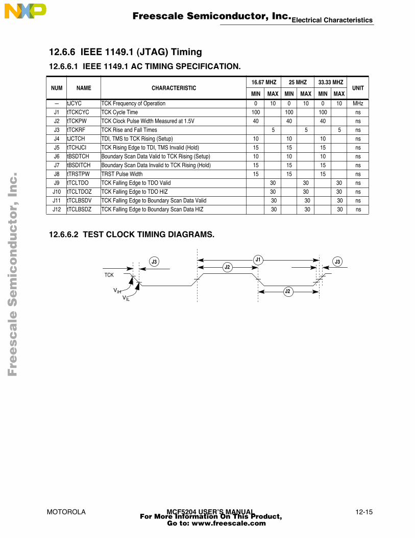
Electrical Characteristics
MOTOROLA MCF5204 USERÕS MANUAL 12-15
12.6.6 IEEE 1149.1 (JTAG) Timing12.6.6.1 IEEE 1149.1 AC TIMING SPECIFICATION.
12.6.6.2 TEST CLOCK TIMING DIAGRAMS.
NUM NAME CHARACTERISTIC16.67 MHZ 25 MHZ 33.33 MHZ
UNITMIN MAX MIN MAX MIN MAX
Ñ tJCYC TCK Frequency of Operation 0 10 0 10 0 10 MHzJ1 tTCKCYC TCK Cycle Time 100 100 100 nsJ2 tTCKPW TCK Clock Pulse Width Measured at 1.5V 40 40 40 nsJ3 tTCKRF TCK Rise and Fall Times 5 5 5 nsJ4 tJCTCH TDI, TMS to TCK Rising (Setup) 10 10 10 nsJ5 tTCHJCI TCK Rising Edge to TDI, TMS Invalid (Hold) 15 15 15 nsJ6 tBSDTCH Boundary Scan Data Valid to TCK Rising (Setup) 10 10 10 nsJ7 tBSDITCH Boundary Scan Data Invalid to TCK Rising (Hold) 15 15 15 nsJ8 tTRSTPW TRST Pulse Width 15 15 15 nsJ9 tTCLTDO TCK Falling Edge to TDO Valid 30 30 30 nsJ10 tTCLTDOZ TCK Falling Edge to TDO HIZ 30 30 30 nsJ11 tTCLBSDV TCK Falling Edge to Boundary Scan Data Valid 30 30 30 nsJ12 tTCLBSDZ TCK Falling Edge to Boundary Scan Data HIZ 30 30 30 ns
TCK
J1
J2
J2J3 J3
ViHVIL
Fre
esc
ale
Se
mic
on
du
cto
r, I
Freescale Semiconductor, Inc.
For More Information On This Product, Go to: www.freescale.com
nc
...

Electrical Characteristics
12-16 MCF5204 USERÕS MANUAL MOTOROLA
12.6.6.3 BOUNDARY SCAN TIMING DIAGRAMS.
12.6.6.4 TEST ACCESS PORT TIMING DIAGRAMS.
TCK
BOUNDARYSCAN DATA
J6 J7
J1
J2
J2
INPUTS
J3
BOUNDARYSCAN DATA
OUTPUTS
J11 J12
J3
J4 J5
TCK
TDITMS
J8
J1
TRST
J2
J2J3
TDO
J9 J10
J3
Fre
esc
ale
Se
mic
on
du
cto
r, I
Freescale Semiconductor, Inc.
For More Information On This Product, Go to: www.freescale.com
nc
...
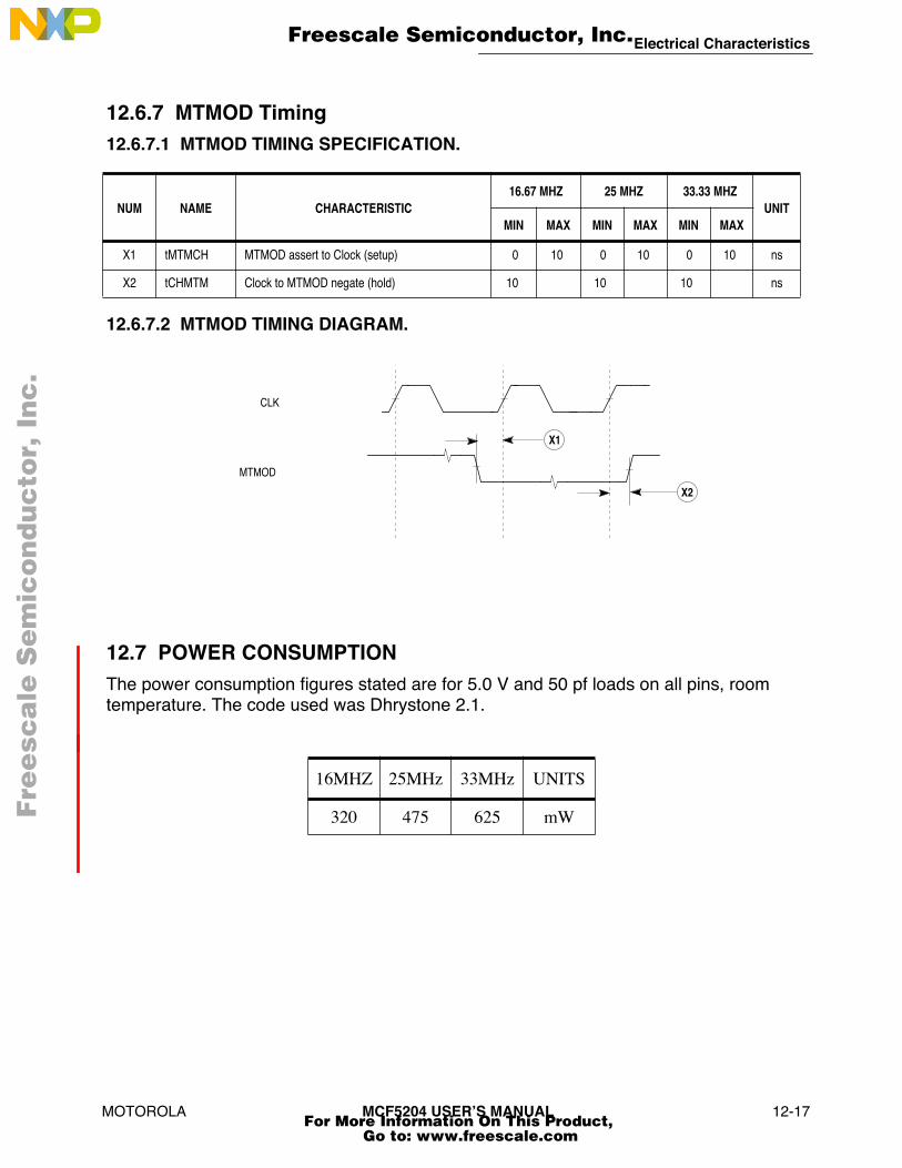
Electrical Characteristics
MOTOROLA MCF5204 USERÕS MANUAL 12-17
12.6.7 MTMOD Timing12.6.7.1 MTMOD TIMING SPECIFICATION.
12.6.7.2 MTMOD TIMING DIAGRAM.
12.7 POWER CONSUMPTIONThe power consumption figures stated are for 5.0 V and 50 pf loads on all pins, room temperature. The code used was Dhrystone 2.1.
NUM NAME CHARACTERISTIC16.67 MHZ 25 MHZ 33.33 MHZ
UNITMIN MAX MIN MAX MIN MAX
X1 tMTMCH MTMOD assert to Clock (setup) 0 10 0 10 0 10 ns
X2 tCHMTM Clock to MTMOD negate (hold) 10 10 10 ns
16MHZ 25MHz 33MHz UNITS
320 475 625 mW
CLK
MTMOD
X2
X1
Fre
esc
ale
Se
mic
on
du
cto
r, I
Freescale Semiconductor, Inc.
For More Information On This Product, Go to: www.freescale.com
nc
...

DATE: 08-21-98
REVISION NO: 0.1
PAGES AFFECTED: SEE CHANGE BARS
F
ree
sca
le S
em
ico
nd
uc
tor,
I
Freescale Semiconductor, Inc.n
c..
.
SECTION 13MECHANICAL DATA
13.1 ORDERING INFORMATION
PACKAGE TYPE FREQUENCY TEMPERATURE ORDER NUMBER
Thin Quad Flat Pack (PU suffix) 16, 25, 33 MHz 0 to 70o C
MCF5204PU16MCF5204PU25MCF5204PU33
MOTOROLA MCF5204 USER’S MANUAL 13-1 For More Information On This Product,
Go to: www.freescale.com

Mechanical Data
Fre
esc
ale
Se
mic
on
du
cto
r, I
Freescale Semiconductor, Inc.n
c..
.
13.2 PACKAGE
Figure 13-1. MC5204 Mechanical Specs
���
�
��� ��� ��� ���
�����
�������$� �������$�
�����������
�� ������$� ��� ��$�
�������$� �������$�
� ������$� ��� ��$�
�� � ���
� ���� ���� ���� ����
� ��� ���� ���� �����
� ���� ��� ����� �����
� ���� ���� ����� ����
���� �� ����� �����
� ������$� �����$�
� ���� ��� ����� �����
� �����#�� �����#��
�� ���� ��� ����� �����
� � �����$� �� ���$�
�� ������$� ������$�
� ���� ��� ����� ����
� � �����$� �� ���$�
�� ������$� ������$�
� ����#�� ������#��
� �����#�� �����#��
θ �� �� �� ��
θ �� ��
θ �� ��
θ �� �� �� ��
!%�$��� ���� $�! � � � � %!��#� �� � "�# � $�
*������ ����� �! %#!��� � ���� $�! � �������%�#�� ��%&� ��� �$ �!��%�� �% �!%%!� !� ����
� � �$ �!� ���� % (�%� %�� ���� (��#� %������ �)�%$ %�� "��$%�� �!�* �% %�� �!%%!�!� %�� "�#%� � �� ��
�� ��%&�$ ���� ��� � � � � %! �� ��%�#�� ���% ��%&� ����
�� ���� $�! $ $ � � ' %! �� ��%�#�� �� �%$��%� � "�� � �%��
� ���� $�! $ � � � � �! !% � ��&�� �!��"#!%#&$�! � ���!(���� "#!%#&$�! �$���� ������� "�# $���� ���� $�! $ � � � � �!� ��&�� �!�� ��$��%�� � � �#���%�#�� �� �% ��%&� ����
�� ���� $�! � �!�$ !% � ��&�� �����#"#!%#&$�! � �����# "#!%#&$�! $���� !% ��&$� %�� ���� (��%� %! �)���� ������������ �� ��&� $"��� ��%(�� "#!%#&$�! � � ������ % ���� !# "#!%#&$�! ������������
�
�
� � � � �
� �
� � � �
��
V1 B1 3X VIEW Y
S1
A1
4X 25 TIPS4X
V
S
A
B
��
��� ��
��
��
�� ��
�
2X 02
$��%� �
"�� � VIEW AA2X 03
C
–L–
����������� � ���
����������� % ���
–M–
����������� %
–H–
–T–
–N–
C2
K
W
�����"�� �
)�� �
G
AB
"��%� �
UJ
D
F
��$����%��$�����������
Θ1
�����������
2XR R1
��
–X– $��������������� $%
13-2 MCF5204 USER’S MANUAL MOTOROLA For More Information On This Product,
Go to: www.freescale.com

Mechanical Data
F
ree
sca
le S
em
ico
nd
uc
tor,
I
Freescale Semiconductor, Inc.n
c..
.
13.3 PIN OUT
MCF5204
O A2 1
pwr VDD 2
pwr VSS 3
O A3 4
O A4 5
O A5 6
O A6 7
O A7 8
pwr VDD 9
pwr VSS 10
O A8 11
O A9 12
O A10 13
O A11 14
O A12 15
pwr VDD 16
pwr VSS 17
O A13 18
O A14 19
O A15 20
O A16 21
O A17 22
pwr VDD 23
pwr VSS 24
O A18 25
OA1
926
PP0
I/OA2
027
PP1
I/OA2
128
NO
WE
29
pwr
VDD
30
pwr
VSS
31
SPP
2I/O
TIN
32
SPP
3I/O
TOU
T33
N
OC
S034
NO
CS1
35
N
OC
S236
IIR
Q0
37
IIR
Q1
38
IIR
Q2
39
IIR
Q3
40
SPP
4I/O
TXD
41
SPP
5I/O
RXD
42
NU
DS
OU
WE
43
NLD
SO
LWE
44
pwr
VDD
45
pwr
VSS
46
NO
RE
47
SPP
6I/O
CTS
48
SPP
7I/O
RTS
49
ATS
I/OBU
SW50
75 D0 I/O
74 VDD pwr
73 VSS pwr
72 D1 I/O
71 D2 I/O
70 D3 I/O
69 D4 I/O
68 D5 I/O
67 VDD pwr
66 VSS pwr
65 D6 I/O
64 D7 I/O
63 D8 I/O
62 D9 I/O
61 D10 I/O
60 VDD pwr
59 VSS pwr
58 D11 I/O
57 D12 I/O
56 D13 I/O
55 D14 I/O
54 D15 I/O
53 VDD pwr
52 VSS pwr
51 DTACK I
100
A1O
99A0
O
98D
DATA
3O
97D
DATA
2O
96VD
Dpw
r
95VS
Spw
r
94D
DATA
1O
93D
DATA
0O
92C
S5O
N
91C
S4O
N
90C
S3O
N
89M
TMO
D3
I
88BK
PTI
TMS
87C
LKI
86D
SCLK
ITR
ST
85D
SII
TDI
84D
SOO
TDO
83M
TMO
D2
I/OPS
T3
82M
TMO
D1
I/OPS
T2
81VD
Dpw
r
80VS
Spw
r
79M
TMO
D0
I/OPS
T1
78H
IZI/O
PST0
77R
ESET
I/O
76TC
LKI
LOGICCACHE DATA CACHE
TAG SRAM
TOP VIEWT
T
MOTOROLA MCF5204 USER’S MANUAL 13-3 For More Information On This Product,
Go to: www.freescale.com
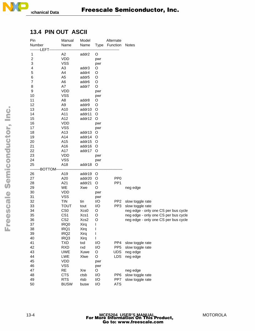
Mechanical Data
F
ree
sca
le S
em
ico
nd
uc
tor,
I
Freescale Semiconductor, Inc.n
c..
.
13.4 PIN OUT ASCIIPin Manual Model AlternateNumber Name Name Type Function Notes--------LEFT-------------------------------------------------------- 1 A2 addr2 O 2 VDD pwr 3 VSS pwr 4 A3 addr3 O 5 A4 addr4 O 6 A5 addr5 O 7 A6 addr6 O 8 A7 addr7 O 9 VDD pwr10 VSS pwr11 A8 addr8 O12 A9 addr9 O13 A10 addr10 O14 A11 addr11 O15 A12 addr12 O16 VDD pwr17 VSS pwr18 A13 addr13 O19 A14 addr14 O20 A15 addr15 O21 A16 addr16 O22 A17 addr17 O23 VDD pwr24 VSS pwr25 A18 addr18 O--------BOTTOM-----------------------------------------------------26 A19 addr19 O27 A20 addr20 O PP028 A21 addr21 O PP129 WE Xwe O neg edge30 VDD pwr31 VSS pwr32 TIN tin I/O PP2 slow toggle rate33 TOUT tout I/O PP3 slow toggle rate34 CS0 Xcs0 O neg edge - only one CS per bus cycle35 CS1 Xcs1 O neg edge - only one CS per bus cycle36 CS2 Xcs2 O neg edge - only one CS per bus cycle37 IRQ0 Xirq I38 IRQ1 Xirq I39 IRQ2 Xirq I40 IRQ3 Xirq I41 TXD txd I/O PP4 slow toggle rate42 RXD rxd I/O PP5 slow toggle rate43 UWE Xuwe O UDS neg edge44 LWE Xlwe O LDS neg edge45 VDD pwr46 VSS pwr47 RE Xre O neg edge48 CTS ctsb I/O PP6 slow toggle rate49 RTS rtsb I/O PP7 slow toggle rate50 BUSW busw I/O ATS
13-4 MCF5204 USER’S MANUAL MOTOROLA For More Information On This Product,
Go to: www.freescale.com

Mechanical Data
F
ree
sca
le S
em
ico
nd
uc
tor,
I
Freescale Semiconductor, Inc.n
c..
.
13.5 PIN OUT ASCII (CONT.)--------RIGHT------------------------------------------------------75 D0 data0 I/074 VDD pwr73 VSS pwr72 D1 data1 I/071 D2 data2 I/070 D3 data3 I/O69 D4 data4 I/068 D5 data5 I/067 VDD pwr66 VSS pwr65 D6 data6 I/064 D7 data7 I/063 D8 data8 I/062 D9 data9 I/061 D10 data10 I/060 VDD pwr58 VSS pwr58 D11 data11 I/057 D12 data12 I/056 D12 data13 I/055 D14 data14 I/054 D15 data15 I/053 VDD pwr52 VSS pwr51 DTACK Xdtack I--------TOP-------------------------------------------------------100 A1 addr1 O99 A0 addr0 O98 DDATA3 ddata3 O97 DDATA2 ddata2 O96 VDD pwr95 VSS pwr94 DDATA1 ddata1 O93 DDATA0 ddata0 O92 CS5 Xcs5 O neg edge - only one CS per bus cycle91 CS4 Xcs4 O neg edge - only one CS per bus cycle90 CS3 Xcs3 O neg edge - only one CS per bus cycle89 MTMOD3 mtmod3 I88 BKPT Xbkpt I TMS87 CLK clk I86 DSCLK dsclk I TRST85 DSI dsi I TDI84 DSO dso O TDO83 PST3 mtmod2 I/O PST82 PST2 mtmod1 I/O PST81 VDD pwr80 VSS pwr79 PST1 mtmod0 I/O PST78 HIZ Xtris I/O PST77 RESET Xreset I/O76 TCLK tclk I
bottom and top both rotate 90 deg. counter clockwise
13-5 MCF5204 USER’S MANUAL MOTOROLA For More Information On This Product,
Go to: www.freescale.com

Fre
esc
ale
Se
mic
on
du
cto
r, I
Freescale Semiconductor, Inc.n
c..
.
INDEXVisit the web site at www.mot.com/ColdFirefor a more comprehensive index.
Aaccess errors 1-4Address Registers 3-2addressing mode 1-7Addressing Modes
index sizing and scaling 1-7postincrement, predecrement, offset, and
indexing 1-7program counter indirect 1-7register indirect 1-7
CCCR 3-3Comand
format 10-10Command
Sequence Diagram 10-10sequence diagram 10-9
DData
Registers 10-12, 10-24data formats 1-7Data Registers 3-2
EExceptions
access errors 1-4
FFIFO stack 8-11
Iindex sizing 1-7Instructions
MOTOROLA MCF5204 USER For More Information
Go to: www.f
STOP 1-4TRAP 1-5
interrupts 1-4handling 8-34requests (UART) 8-3
Llogical address space 1-7looping modes 8-12low-power stop mode 1-4
Ooperand size 1-7
Pprivilege modes 1-4Processing States
normal processing 1-5normal, exception, halted 1-4
programming modelinteger unit Portion 3-2
RRead
Memory Location Command 10-9Registers
A6–A0 3-2address registers 1-6cache control register 1-7condition code register 1-6D7–D0 3-2index registers 1-6program counter 1-6stack pointer 1-6Status Register (SR)
S-bit 1-4vector base register 1-7
SSignals
PSTx 2-10Special Modes of Operation
’S MANUAL I-1
INDEX
On This Product,reescale.com

Index
INDEX
F
ree
sca
le S
em
ico
nd
uc
tor,
I
Freescale Semiconductor, Inc.n
c..
.
low-power stop mode 1-4SR 3-4supervisor programming model 1-5
TTCN1, TCN2 9-5TCR1, TCR2 9-5TER1, TER2 9-6timer module 9-1
block diagram 9-2capture registers 9-5counter 9-5event registers 9-6general-purpose timer units 9-2mode register 9-4reference registers 9-5
TMR1, TMR2 9-4TRR1, TRR2 9-5
UUACR 8-29UART module
auxiliary control register 8-29clock select register 8-24command register 8-24I/O driver routines 8-34initialization routines 8-34input port change register 8-28input port register 8-32interrupt mask register 8-30interrupt status register 8-29interrupt vector register 8-32receive buffer 8-28status register 8-21timer upper preload registers 8-32timer/counter 8-3transmitter buffer 8-28valid start bit 8-9
UBG1, 2 8-32UCR 8-24UCSR 8-24UIMR 8-30UIP 8-32UIPCR 8-28UISR 8-29UIVR 8-32URB 8-28user programming model 1-5USR 8-21UTB 8-28
I-2 MCF5204 USER’S For More Information
Go to: www.f
VVBR 3-5
MANUAL MOTOROLA On This Product,reescale.com