Embed Size (px)
Citation preview
Freescale SemiconductorProduct Brief
MPC5533PBRev. 0, 9/2007
Table of ContentsBlock Diagram . . . . . . . . . . . . . . . . . . . . . . . . . . . . . . . . . 3MPC5533 Features List. . . . . . . . . . . . . . . . . . . . . . . . . . 4MPC5533 Detailed Features . . . . . . . . . . . . . . . . . . . . . 13Chip Configuration. . . . . . . . . . . . . . . . . . . . . . . . . . . . . 22Documentation . . . . . . . . . . . . . . . . . . . . . . . . . . . . . . . 22
MPC5533 MicrocontrollerProduct Brief
The MPC5533 MCU is a member of the family of next generation microcontrollers built on the Power ArchitectureTM Book E technology. This family of parts contains many new features coupled with high-performance CMOS technology to provide substantial reduction of cost per feature and significant performance improvement over the MPC500 family. Refer to MPC5500 Family Overview (EB659), for feature-set comparisons, block diagrams, and more information on the devices.
The host processor core of the MPC5533 is compatible with the Book E architecture. It is 100% user-mode compatible (with floating-point library) with the classic Power Architecture instruction set. The Book E architecture has enhancements that improve the architecture’s fit in embedded applications. This core also has additional instructions, including digital signal processing (DSP) instructions, beyond the classic instruction set.
The host processor core of the MPC5533 also includes an instruction set enhancement allowing variable length encoding (VLE). This allows optional encoding of mixed
12345
© Freescale Semiconductor, Inc., 2007. All rights reserved.

16- and 32-bit instructions. With this enhancement, it is possible to achieve significant code size footprint reduction.
The MPC5533 has a single level of memory hierarchy consisting of on-chip SRAM and internal flash memory. The SRAM and the flash memory can hold instructions and data.
The complex I/O timer functions of MPC5533 are performed by an enhanced time processor unit engine (eTPU). The eTPU engine controls 32 hardware channels. The eTPU is enhanced over the MPC500 family’s TPU by providing 24-bit timers, double-action hardware channels, variable number of parameters per channel, angle clock hardware, and additional control and arithmetic instructions. The eTPU can be programmed using a high-level programming language.
Off-chip communication is performed by a suite of serial protocols including CANs, enhanced SPIs (deserialize/serialize peripheral interface) and SCIs. The DSPIs support pin reduction through hardware serialization and deserialization of timer channels and GPIO signals.
The MPC5533 MCU has an on-chip 34-channel enhanced queued dual analog-to-digital converter (eQADC), with 5 V conversion range.
The system integration unit (SIU) performs several chip-wide configuration functions. Pad configuration and general-purpose input and output (GPIO) are controlled from the SIU. External interrupts and reset control are also found in the SIU. The internal multiplexer sub-block (IMUX) provides multiplexing of eQADC trigger sources, daisy chaining the DSPIs and external interrupt signal multiplexing.
On-chip modules include:• Single issue, 32-bit Book E compatible CPU core complex
— Includes VLE enhancements for code size footprint reduction• 32-channel enhanced direct memory access controller (eDMA)• Interrupt controller (INTC) capable of handling 178 selectable-priority interrupt sources• Frequency modulated phase-locked loop (PLL)• System integration unit (SIU)• 768-KB on-chip flash memory with flash control unit (FCU)• 48-KB on-chip static RAM (SRAM)• Boot assist module (BAM)• 32-channel enhanced time processor unit (eTPU)• Enhanced 5 V queued analog-to-digital converter (eQADC)• Deserial serial peripheral interface (DSPI) module • Enhanced serial communication interface (eSCI) module (with LIN support)• Two controller area network (FlexCAN) modules• Nexus development interface (NDI) per IEEE-ISTO 5001-2003 standard• Device/board test support per Joint Test Action Group (JTAG) of IEEE (IEEE 1149.1)• On-chip voltage regulator controller for regulating 3.3 V down to 1.5 V for core logic
MPC5533 Microcontroller Product Brief, Rev. 0
Freescale Semiconductor2
Block Diagram
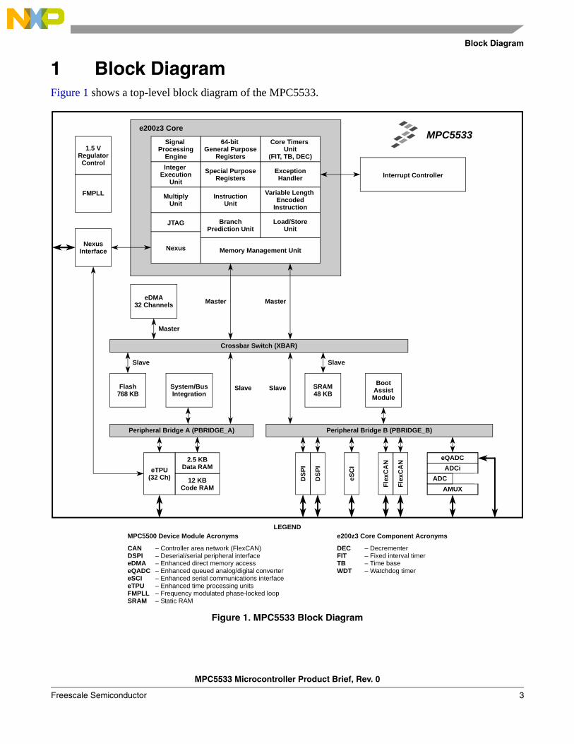
1 Block DiagramFigure 1 shows a top-level block diagram of the MPC5533.
Figure 1. MPC5533 Block Diagram
LEGEND
Integer Execution
Unit
MultiplyUnit
e200z3 Core
Nexus
JTAG
eSC
I
eQADC
AMUXADC
ADCi2.5 KB
eTPU(32 Ch) 12 KB
Code RAM
Data RAM
1.5 VRegulator
Control
FMPLL
Signal Processing
Engine
InstructionUnit
64-bit General Purpose
Registers
Special PurposeRegisters
BranchPrediction Unit
Core Timers Unit
(FIT, TB, DEC)
ExceptionHandler
Variable Length Encoded
Instruction
NexusInterface
Interrupt Controller
eDMA32 Channels
Master
Load/StoreUnit
Slave
Peripheral Bridge A (PBRIDGE_A)
System/BusIntegration
Slave
Master
Flash768 KB
Slave
Peripheral Bridge B (PBRIDGE_B)
Crossbar Switch (XBAR)
BootAssistModule
Slave
Flex
CA
N
Flex
CA
N
DSP
I
DSP
I
SRAM48 KB
e200z3 Core Component Acronyms
DEC – DecrementerFIT – Fixed interval timerTB – Time baseWDT – Watchdog timer
MPC5500 Device Module Acronyms
CAN – Controller area network (FlexCAN)DSPI – Deserial/serial peripheral interfaceeDMA – Enhanced direct memory accesseQADC – Enhanced queued analog/digital convertereSCI – Enhanced serial communications interfaceeTPU – Enhanced time processing unitsFMPLL – Frequency modulated phase-locked loopSRAM – Static RAM
Memory Management Unit
Master
MPC5533
MPC5533 Microcontroller Product Brief, Rev. 0
Freescale Semiconductor 3

MPC5533 Features List
2 MPC5533 Features ListThis section provides a high-level description of the features in the MPC5533.
2.1 Operating Parameters• Fully static operation, 0 MHz to 80 MHz• –40° to 150° C junction temperature (125° C ambient temperature)• Low-power design
— Less than 0.8 Watts power dissipation— Designed for dynamic power management of core and peripherals— Software controlled clock gating of peripherals— Separate power supply for stand-by operation for a portion of SRAM
• Fabricated in 0.13 μm process• 1.5 V internal logic• Input and output pins with 3.0 V to 5.5 V range
— 35% and 65% VDDE CMOS switch levels (with hysteresis)— Selectable hysteresis— Selectable slew rate control
• Nexus pins support 1.6 V to 3.6 V operation— Selectable drive strength control— Unused pins configurable as GPIO
• Designed with EMI reduction techniques— Frequency modulated phase-locked loop— On-chip bypass capacitance— Selectable slew rate and drive strength
2.2 e200z3 Core Processor• Single issue, 32-bit Power Architecture Book E compatible CPU
— In-order execution and retirement— Precise exception handling— User-mode binary compatible with MPC5xx except floating point instructions
• Variable Length Encoding Enhancements— e200z3 core supports both Book E and VLE instruction sets— Allows optional encoding of mixed 16 and 32 bit instructions— Results in smaller code size footprint
MPC5533 Microcontroller Product Brief, Rev. 0
Freescale Semiconductor4

MPC5533 Features List
— Regions of the memory map are designated as Book E or VLE, based on configuration of the memory management unit (MMU)
• Branch processing unit— Dedicated branch address calculation adder— Branch acceleration using branch lookahead instruction buffer
• Load/store unit— Fully pipelined— Big- and little endian support— Misaligned access support— Zero load-to-use pipeline bubbles— Supports throughput of one load or store operation per cycle— Memory interface support for saving and restoring two registers per cycle
• Thirty-two 64-bit general purpose registers (GPRs)• MMU with 16-entry fully-associative translation look-aside buffer (TLB)• Separate instruction bus and load/store bus• Vectored interrupt support• Interrupt latency < 116 ns at 80 MHz (measured from interrupt request to execution of first
instruction of interrupt exception handler)• Reservation instructions for implementing read-modify-write constructs (CPU master only)• Numerics and DSP
— Saturated, unsaturated, and fractional arithmetic— Support for DSP addressing modes— Pipelined dual 32x32 MAC with one clock throughput
• Signal processing extension APU — Operating on all 32 GPRs that are all extended to 64 bits wide— Single instruction multiple data (SIMD) provides a full compliment of vector and scalar
integer and floating-point arithmetic operations (including integer vector MAC and MUL operations)
— Provides rich array of extended 64-bit loads and stores to/from extended GPRs— Fully code compatible with e200z6 core
• Floating point — IEEE 754 compatible with software wrapper— Scalar single precision in hardware; double precision with software library— Conversion instructions between single precision floating point and fixed point— Fully code compatible with e200z6 core
• Long cycle time instructions, except for guarded loads, do not increase interrupt latency
MPC5533 Microcontroller Product Brief, Rev. 0
Freescale Semiconductor 5

MPC5533 Features List
• Extensive system development support through Nexus debug port
2.3 Crossbar Switch (XBAR)• Three master ports, four slave ports
— Masters: CPU instruction bus; CPU load/store bus; eDMA— Slaves: Flash; SRAM; peripheral bridge A; peripheral bridge B
• 32-bit internal address bus, 64-bit internal data bus
2.4 Enhanced Direct Memory Access (eDMA) Controller• 32 channels support independent 8-, 16-, or 32-bit single-value or block transfers• Supports variable sized queues and circular queues• Source and destination address registers are independently configured to post-increment or
remain constant• Each transfer is initiated by a peripheral, CPU, or eDMA channel request• Each eDMA channel can optionally send an interrupt request to the CPU on completion of a
single value or block transfer• All data movement via dual-address transfers: read from source, write to destination• Programmable source and destination addresses, transfer size, plus support for enhanced
addressing modes• Transfer control descriptor organized to support two-deep, nested transfer operations• An inner data transfer loop defined by a minor byte transfer count• An outer data transfer loop defined by a major iteration count• Channel activation via one of three methods:
— Explicit software initiation— Initiation via a channel-to-channel linking mechanism for continuous transfers— Peripheral-paced hardware requests (one per channel)
• Support for fixed-priority and round-robin channel arbitration• Channel completion reported via optional interrupt requests• One interrupt per channel, optionally asserted at completion of major iteration count• Error termination interrupts are optionally enabled• Support for scatter-gather DMA processing• Channel transfers can be suspended by a higher priority channel
2.5 Interrupt Controller (INTC)• Unique 9-bit vector per interrupt source for 178 interrupt sources
MPC5533 Microcontroller Product Brief, Rev. 0
Freescale Semiconductor6
MPC5533 Features List
• Eight software setable interrupt sources• 16 priority levels with fixed hardware arbitration within priority levels for each interrupt source• Priority elevation for shared resources
2.6 Frequency Modulated Phase-Locked Loop (FMPLL)• Input clock frequency from 8 MHz to 20 MHz• Current controlled oscillator (ICO) range from 48 MHz to maximum device frequency• Reduced frequency divider (RFD) for reduced frequency operation without forcing the FMPLL to
re-lock• Four modes of operation
— Bypass mode— PLL normal mode with crystal reference (default)— PLL normal mode with external oscillator reference— PLL dual controller mode for EXTAL to CLKOUT skew minimization
• Programmable frequency modulation— Modulation enabled/disabled through software— Triangle wave modulation— Programmable modulation depth (1% or 2% deviation from center frequency)— Programmable modulation frequency dependent on reference frequency
• Lock detect circuitry reports when the FMPLL has achieved frequency lock and continuously monitors lock status to report loss of lock conditions
• Programmable interrupt request on system reset or loss of lock• Loss-of-clock (LOC) detection for reference and feedback clocks• Programmable interrupt request on system reset or loss of clock• Self-clocked mode (SCM) operation
2.7 System Integration Unit (SIU)• System configuration
— MCU reset configuration via external pins— Pad configuration control
• System reset monitoring and generation— Power-on reset support— Reset status register provides last reset source to software— Glitch detection on reset input— Software controlled reset assertion
MPC5533 Microcontroller Product Brief, Rev. 0
Freescale Semiconductor 7

MPC5533 Features List
• External interrupt— Fifteen interrupt requests— Rising or falling edge event detection— Programmable digital filter for glitch rejection
• GPIO— GPIO function on 86 I/O pins— Dedicated input and output registers for setting each GPIO pin
• Internal multiplexing— Allows serial and parallel chaining of DSPIs— Allows flexible selection of eQADC trigger inputs— Allows selection of interrupt requests between external pins and DSPI
2.8 Error Correction Status Module (ECSM)• Configurable error-correcting codes (ECC) reporting• ECC performs single-bit correction, double-bit detection on 32-bit data element
2.9 On-Chip Flash• 768 KB burst flash memory
— Configured as 48K x 128 bits— 10 blocks (2×16K + 2×48K + 2×64K + 4×128 KB) to support features such as boot block,
operating system block and EEPROM emulation— 1 KB shadow row compatible with all other parts in the family for storing censorship and
configuration information (censorship protection scheme to prevent flash content visibility)— Accessed via a 64-bit wide bus interface
• Quadruple 128-bit wide prefetch/burst buffers to provide single cycle in-line accesses (prefetch buffers can be configured to prefetch code or data or both)
• Hardware read-while-write feature that allows blocks to be erased/programmed while other blocks are being read (used for EEPROM emulation and data calibration)
• Page mode (128-bits) programming for rapid end-of-line programming• Hardware programming state machine• Supports a 64-bit data bus; Byte, halfword, word, and doubleword reads are supported; Only
aligned word and doubleword writes are supported• Hardware and software configurable read and write access protections on a per-master basis• Interface to the flash array controller is pipelined with a depth of 1, allowing overlapped accesses
to proceed in parallel for interleaved or pipelined Flash array designs• Configurable access timing allowing use in a wide range of system frequencies
MPC5533 Microcontroller Product Brief, Rev. 0
Freescale Semiconductor8

MPC5533 Features List
• Multiple-mapping support and mapping-based block access timing (0–31 additional cycles) allowing use for emulation of other memory types
• Software programmable block program/erase restriction control• Erase of selected block(s)• Read page size of 128 bits (4 words)• Embedded hardware program and erase algorithm• Erase suspend, program suspend, and erase-suspended program• Shadow information stored in non-volatile shadow block• Independent program/erase of the shadow block
2.10 On-Chip Static RAM (SRAM)• Supports read/write accesses mapped to the SRAM memory from any master• 48 KB general purpose RAM of which 32 KB are on standby power• Byte, halfword, word, and doubleword addressable
2.11 Boot assist module (BAM)• Enables and manages the transition of MCU from reset to user code execution in the following
configurations:— Execution from internal flash— Download and execution of code via FlexCAN or eSCI
• Sets up MMU to cover all resources and mapping all physical address to logical addresses with minimum address translation
• Sets up the MMU to allow user boot code to execute as Book E code (default) or as VLE code• Location and detection of user boot code• Automatic switch to serial boot mode if internal flash is blank or invalid• Supports user programmable 64-bit password protection for serial boot mode• Supports serial bootloading of either Book E code (default) or VLE code• Supports censorship protection for internal flash memory• Provides an option to enable the core watchdog timer
2.12 Enhanced Time Processor Unit (eTPU)• eTPU engine is an event triggered VLIW processor timer subsystem• High-level assembler/compiler• 32 channels• 24-bit timer resolution
MPC5533 Microcontroller Product Brief, Rev. 0
Freescale Semiconductor 9
MPC5533 Features List
• 12 KB code memory and 2.5 KB data memory• Variable number of parameters allocatable per channel• Double match/capture channels• Angle clock hardware support• Shared time or angle counter bus (STAC) for all eTPU channels• DMA and interrupt request support• Nexus Class 3 Debug support (with some Class 4 support)
2.13 Enhanced Queued A/D Converter (eQADC)• ADC
— 12-bit A/D resolution— Up to 10 bit accuracy at 400 ksample/s and 8 bit accuracy at 800 ksample/s— Differential conversions— Single-ended signal range from 0 to 5 V— Sample times of 2 (default), 8, 64, or 128 ADC clock cycles— Provides time stamp information when requested— Parallel interface to eQADC CFIFOs and RFIFOs— Supports right-justified unsigned and signed formats for conversion results
• 0 – 5 V common mode conversion range• 34 single-ended input channels, with support for up to 11 additional channels using external
multiplexers • Eight channels can be used as four pairs of differential analog input channels• Supports six FIFO queues with fixed priority. • Queue modes with priority-based preemption, initiated by software command or internal (eTPU)
or external triggers• DMA and interrupt request support• Supports all functional modes from QADC (MPC5xx family)• Full-duplex synchronous serial interface (SSI) to an external device
— Free-running clock for use by an external device— Supports a 26-bit message length
• Priority based CFIFOs— Supports six CFIFOs with fixed priority. The lower the CFIFO number, the higher its priority.
When commands of distinct CFIFOs are bound for the same CBuffer, the higher priority CFIFO is always served first
— Supports software and hardware trigger modes to arm a particular CFIFO— Generates interrupt when command coherency is not achieved
MPC5533 Microcontroller Product Brief, Rev. 0
Freescale Semiconductor10
MPC5533 Features List
• External hardware triggers— Supports rising-edge, falling-edge, high-level and low-level triggers— Supports configurable digital filter
• Supports four external 8-to-1 muxes that can expand the input channels
2.14 Deserial serial peripheral interface (DSPI) • Two DSPI modules• SPI
— Full-duplex communication ports with interrupt and DMA request support— Supports all functional modes from QSPI sub-block of QSMCM (MPC5xx family)— Support for queues in RAM— Six chip selects, expandable to 64 with external demultiplexers— Programmable frame size, baud rate, clock delay, and clock phase on a per-frame basis— Modified SPI mode for interfacing to peripherals with longer setup time requirements
• Deserial serial interface (DSI)— Pin reduction by hardware serialization and deserialization of eTPU channels— Chaining of DSI sub-blocks— Triggered transfer control and change in data transfer control (for reduced EMI)
2.15 Enhanced Serial Communication Interface (eSCI)• UART mode provides NRZ format and half or full duplex interface• eSCI bit rate up to 1 Mb/s• Advanced error detection and optional parity generation and detection• Separately enabled transmitter and receiver• eDMA support (on one of the eSCI modules only)• 13-bit baud rate selection• Programmable 8-bit or 9-bit word length (data format)• LIN support
— Autonomous transmission of entire frames— Configurable to support all revisions of the LIN standard— Automatic parity bit generation— Double stop bit after bit error— 10-bit or 13-bit break support
• Separately enabled transmitter and receiver• Programmable transmitter output parity
MPC5533 Microcontroller Product Brief, Rev. 0
Freescale Semiconductor 11

MPC5533 Features List
• Two receiver wake-up methods: idle line and address mark• Interrupt-driven operation with flags• Receiver framing error detection • Hardware parity checking • 1/16 bit-time noise detection • Two channel eDMA interface
2.16 FlexCAN• Two FlexCAN modules• 64 message buffers each (0 to 8 bytes data length)• Based on and including all existing features of the Freescale TouCAN module• Full implementation of the CAN protocol specification, version 2.0B
— Standard data and remote frames— Extended data and remote frames— Zero to eight bytes data length— Programmable bit rate up to 1 Mb/s
• Programmable acceptance filters• Short latency time for high-priority transmit messages• Arbitration scheme according to message ID or message buffer number• Listen only mode capabilities• Programmable clock source: system clock or oscillator clock• Content-related addressing• Each message buffer configurable as Rx or Tx, all supporting standard and extended messages• Includes 1056 bytes of embedded memory for message buffer storage• Programmable loop-back mode supporting self-test operation• Three programmable mask registers• Programmable transmit-first scheme: lowest ID or lowest buffer number• Time stamp based on 16-bit free-running timer• Global network time, synchronized by a specific message• Maskable interrupts• Independent of the transmission medium (an external transceiver is assumed)• Multi-master concept• High immunity to EMI• Short latency time due to an arbitration scheme for high-priority messages• Low-power mode, with programmable wake-up on bus activity
MPC5533 Microcontroller Product Brief, Rev. 0
Freescale Semiconductor12

MPC5533 Detailed Features
2.17 Nexus Development Interface (NDI)• Per IEEE-ISTO 5001-2003• Real-time development support for e200z3 core and eTPU engine through Nexus Class 3
(selected Class 4 support)• Read and write access
— Run-time access of entire memory map— Calibration (table constants calibrated using MMU and internal RAM; scalar constants
calibrated using cache line locking)• Configured via the IEEE 1149.1 (JTAG) port• Reduced bandwidth mode for reduced pin usage
2.18 IEEE 1149.1 JTAG Controller (JTAGC)• IEEE 1149.1-2001 Test Access Port (TAP) interface four pins (TDI, TMS, TCK, and TDO)• A JCOMP input that provides the ability to share the TAP (selectable modes of operation include
JTAGC/debug or normal system operation)• Selectable modes of operation include JTAGC/debug or normal system operation.• A 5-bit instruction register that supports these IEEE 1149.1-2001 defined instructions:
— BYPASS, IDCODE, EXTEST, SAMPLE, SAMPLE/PRELOAD, HIGHZ, CLAMP• A 5-bit instruction register that supports the additional public instructions:
— ACCESS_AUX_TAP_NPC, ACCESS_AUX_TAP_ONCE, ACCESS_AUX_TAP_eTPU• Three test data registers: a bypass register, a boundary scan register, and a device identification
register• A TAP controller state machine that controls the operation of the data registers, instruction
register and associated circuitry
2.19 On-Chip Voltage Regulator Controller• Uses external NPN bipolar transistor• Regulates 3.3 V down to 1.5 V for the core logic
3 MPC5533 Detailed FeaturesThe following sections provide detailed information about each of the on-chip modules.
3.1 e200z3 Core OverviewThe e200z3 processor uses a four-stage pipeline for instruction execution. The instruction fetch (stage 1), instruction decode/register file read/effective address calculation (stage 2), execute/memory access
MPC5533 Microcontroller Product Brief, Rev. 0
Freescale Semiconductor 13

MPC5533 Detailed Features
(stage 3), and register writeback (stage 4) stages operate in an overlapped fashion, allowing single clock instruction execution for most instructions.
The integer execution unit consists of a 32-bit arithmetic unit (AU), a logic unit (LU), a 32-bit barrel shifter (Shifter), a mask-insertion unit (MIU), a condition register manipulation unit (CRU), a count-leading-zeros unit (CLZ), a 32x32 hardware multiplier array, result feed-forward hardware, and support hardware for division.
Most arithmetic and logical operations are executed in a single cycle with the exception of the divide instructions. A count-leading-zeros unit operates in a single clock cycle. The instruction unit contains a PC incrementer and a dedicated branch address adder to minimize delays during change of flow operations. Sequential prefetching is performed to ensure a supply of instructions into the execution pipeline. Branch target prefetching is performed to accelerate taken branches. Prefetched instructions are placed into an instruction buffer capable of holding six instructions.
Branches can also be decoded at the instruction buffer and branch target addresses calculated prior to the branch reaching the instruction decode stage, allowing the branch target to be prefetched early. When a branch is detected at the instruction buffer, a prediction may be made on whether the branch is taken or not. If the branch is predicted to be taken, a target fetch is initiated and its target instructions are placed in the instruction buffer following the branch instruction. Many branches take zero cycle to execute by using branch folding. Branches are folded out from the instruction execution pipe whenever possible. These include unconditional branches and conditional branches with condition codes that can be resolved early.
Conditional branches that are not taken and not folded execute in a single clock. Branches with successful target prefetching that are not folded have an effective execution time of one clock. All other taken branches have an execution time of two clocks. Memory load and store operations are provided for byte, halfword, and word (32-bit) data with automatic zero or sign extension of byte and halfword load data as well as optional byte reversal of data. These instructions can be pipelined to allow effective single cycle throughput. Load and store multiple word instructions allow low overhead context save and restore operations. The load/store unit contains a dedicated effective address adder to allow effective address generation to be optimized. Also, a load-to-use dependency does not incur any pipeline bubbles for most cases.
The CRU supports the condition register and condition register operations defined by the Power Architecture technology. The condition register consists of eight 4-bit fields that reflect the results of certain operations, such as move, integer and floating-point compare, arithmetic, and logical instructions, and provides a mechanism for testing and branching. Vectored and autovectored interrupts are supported by the CPU. Vectored interrupt support is provided to allow multiple interrupt sources to have unique interrupt handlers invoked with no software overhead.
The hardware floating-point unit uses the IEEE-754 single-precision floating-point format and supports single-precision floating-point operations in a pipelined fashion. The general purpose register file is used for source and destination operands, with a unified storage model for single-precision floating-point data types of 32-bits and the normal integer type. Single-cycle floating-point add, subtract, multiply, compare, and conversion operations are provided. Divide instructions are multi-cycle and are not pipelined.
The signal processing extension (SPE) auxiliary processing unit (APU) provides hardware SIMD operations and supports a full compliment of dual integer arithmetic operations including multiply accumulate (MAC) and dual-integer multiply (MUL) in a pipelined fashion. The general-purpose register
MPC5533 Microcontroller Product Brief, Rev. 0
Freescale Semiconductor14

MPC5533 Detailed Features
file is enhanced such that all 32 of the GPRs are extended to 64 bits wide and are used for source and destination operands, with a unified storage model for 32 x 32 MAC operations that generate greater than 32-bit results.
The majority of scalar and vector operations (including MAC and MUL) are executed in a single clock cycle. Scalar and Vector divides take multiple clocks. The SPE APU also provides extended load and store operations to support the transfer of data to and from the extended 64 bit GPRs. This SPE APU is fully binary compatible with the e200z6 SPE APU used in MPC5554 and MPC5553.
The CPU includes support for variable length encoding (VLE) instruction enhancements. This allows the optional execution of an alternate instruction set consisting of a mixture of 16-bit and 32-bit instructions. This results in a significantly smaller code size footprint without affecting performance noticeably. The e200z3 core supports both the Book E and VLE instruction sets.
3.2 Crossbar Switch (XBAR)The XBAR multi-port crossbar switch supports simultaneous connections between three master ports and slave ports.
• Three master ports:— Core CPU—Instruction— Core CPU—Data— eDMA
• slave ports— Flash (64-bit data access)— Calibration Bus (64-bit data access)— SRAM (64-bit data access)— Peripheral bridge A (32-bit data access)— Peripheral bridge B (32-bit data access)
The crossbar allows for concurrent transactions to occur from any master port to any slave port. It is possible for all master ports and slave ports to be in use at the same time as a result of independent master requests. If a slave port is simultaneously requested by more than one master port, arbitration logic selects the higher priority master and grants it ownership of the slave port. All other masters requesting that slave port must wait until the higher priority master completes its transactions. By default, requesting masters will be treated with equal priority and will be granted access to a slave port in round-robin fashion, based upon the ID of the last master to be granted access.
3.3 Enhanced Direct Memory Access (eDMA) ControllerThe eDMA controller is a second-generation module capable of performing complex data movements via 32 programmable channels, with minimal intervention from the host processor. The hardware microarchitecture includes a DMA engine that performs source and destination address calculations, and the actual data movement operations, along with an SRAM-based memory containing the transfer control descriptors (TCD) for the channels. This implementation is used to minimize the overall block size.
MPC5533 Microcontroller Product Brief, Rev. 0
Freescale Semiconductor 15
MPC5533 Detailed Features
3.4 Interrupt Controller (INTC)The INTC provides priority-based preemptive scheduling of interrupt requests, suitable for statically scheduled hard real-time systems. The INTC allows interrupt request servicing from up to 178 interrupt sources.
For high-priority interrupt requests, the time from the assertion of the interrupt request from the peripheral to when the processor is executing the interrupt service routine (ISR) has been minimized. The INTC provides a unique vector for each interrupt request source for quick determination of which ISR needs to be executed. It also provides an ample number of priorities so that lower priority ISRs do not delay the execution of higher priority ISRs. To allow the appropriate priorities for each source of interrupt request, the priority of each interrupt request is software configurable.
When multiple tasks share a resource, coherent accesses to that resource need to be supported. The INTC supports the priority ceiling protocol for coherent accesses. By providing a modifiable priority mask, the priority can be raised temporarily so all tasks that share the resource cannot preempt each other.
Multiple processors can assert interrupt requests to each other through software setable interrupt requests. These same software setable interrupt requests also can be used to break the work involved in servicing an interrupt request into high-priority and low-priority portions. The high-priority portion is initiated by a peripheral interrupt request, but then the ISR asserts a software setable interrupt request to finish the servicing in a lower priority ISR. Therefore these software setable interrupt requests can be used instead of the peripheral ISR scheduling a task through the RTOS.
3.5 Frequency Modulated Phase-Locked Loop (FMPLL)The FMPLL allows the user to generate high-speed system clocks from an 8 MHz to 20 MHz crystal oscillator or external clock generator. Further, the FMPLL supports programmable frequency modulation of the system clock. The FMPLL multiplication factor, output clock divider ratio, modulation depth, and modulation rate are all software configurable.
3.6 System Integration Unit (SIU)The SIU controls MCU reset configuration, pad configuration, external interrupt, general-purpose I/O (GPIO), internal peripheral multiplexing, and the system reset operation. The reset configuration block contains the external pin boot configuration logic. The pad configuration block controls the static electrical characteristics of I/O pins. The GPIO block provides uniform and discrete input/output control of the I/O pins of the MCU. The reset controller performs reset monitoring of internal and external reset sources, and drives the RSTOUT pin. The SIU is accessed by the e200z3 core through the crossbar switch.
For more information on configuring the MPC5533 at reset see Section 4, “Chip Configuration.”
3.7 On-Chip FlashThe MPC5533 provides 768 KB of programmable, non-volatile, flash memory. The non-volatile memory (NVM) can be used for instruction and/or data storage. The flash module interfaces the system bus to a dedicated Flash memory array controller. It supports a 64-bit data bus width at the system bus port, and a
MPC5533 Microcontroller Product Brief, Rev. 0
Freescale Semiconductor16
MPC5533 Detailed Features
128-bit read data interface to flash memory. The module contains a four-entry, 128-bit prefetch buffer and a prefetch controller which prefetches sequential lines of data from the Flash array into the buffer. Prefetch buffer hits allow no-wait responses. Normal flash array accesses are registered and are forwarded to the system bus on the following cycle, incurring three wait-states. Prefetch operations may be automatically controlled, and may be restricted to servicing a single bus master. Prefetches may also be restricted to being triggered for instruction or data accesses.
3.8 SRAMThe MPC5533 SRAM module provides a general-purpose 48 KB memory block. The first 32K block of the SRAM is powered by its own power supply pin, called VSTBY. This allows the contents of this memory region to be preserved when the rest of the MCU is powered down.
ECC handling is done on a 32-bit boundary and is completely software compatible with MPC5500 family devices with an e200z6 core and 64-bit wide ECC syndrome. Because the e200z3 core in MPC5533 is a cacheless processor, the platform RAM is organized on a 32-bit boundary versus the 64-bit organization used on other MPC5500 family MCUs based on the e200z6 core.
3.9 BAMThe BAM is a block of read-only memory that is hard-coded by Freescale and is identical for all MPC5500 family MCUs with an e200 core. The BAM program is executed every time the MCU is powered-on or reset in normal mode. The BAM supports two different modes of booting. They are:
• Booting from internal flash memory • Serial boot loading (a program is downloaded into RAM via eSCI or the FlexCAN and then
executed)
The BAM also reads the reset configuration halfword (RCHW) from internal flash memory and configures the MPC5533 hardware accordingly.
For more information on configuring the MPC5533 at reset see Section 4, “Chip Configuration.”
3.10 Enhanced Time Processor Unit (eTPU)The eTPU is an enhanced coprocessor designed for timing control. Operating in parallel with the host CPU, the eTPU processes instructions and real-time input events, performs output waveform generation, and accesses shared data without host intervention. Consequently, for each timer event, the host CPU setup and service times are minimized or eliminated. A powerful timer subsystem is formed by combining the eTPU with its own instruction and data RAM. High-level assembler/compiler and documentation allows customers to develop their own functions on the eTPU.
The eTPU is an enhanced version of the TPU module implemented on the MC68332 and MPC500 products. Enhancements of the eTPU include a more powerful processor which handles high-level C code efficiently and allows for more functionality and increased performance. Although there is no compatibility at microcode level, the eTPU maintains several features of older TPU versions and is conceptually almost identical. The eTPU library is a superset of the standard TPU library functions
MPC5533 Microcontroller Product Brief, Rev. 0
Freescale Semiconductor 17

MPC5533 Detailed Features
modified to take advantage of enhancements in the eTPU. These, along with a C compiler, make it relatively easy to port older applications. By providing source code for the Freescale library, it is possible for the eTPU to support the users own function development.
The eTPU includes these distinctive features:• 32 channels, each channel is associated with one input and one output signal.
— Enhanced input digital filters on the input pins for improved noise immunity.— Each identical, orthogonal channel can perform any time function. Each time function can be
assigned to more than one channel at a given time, so each signal can have any functionality.— Each channel has an event mechanism that supports single and double action functionality in
various combinations. It includes two 24-bit capture registers, two 24-bit match registers, 24-bit greater-equal and equal-only comparators
— Input and output signal states visible from the host• Two independent 24-bit time bases for channel synchronization:
— First time base clocked by system clock with programmable prescale division from 2 to 512 (in steps of 2), or by output of second time base prescaler
— Second time base counter can work as a continuous angle counter, enabling angle based applications to match angle instead of time.
— Both timebases visible from the host• Event-triggered microengine:
— Fixed-length instruction execution in two-system-clock microcycle— 12 KB of code memory (SCM)— 2.5 KB of parameter (data) RAM (SPRAM)— Parallel execution of data memory, ALU, channel control and flow control sub-instructions in
selected combinations— 32-bit microengine registers and 24-bit wide ALU, with one microcycle addition and
subtraction, absolute value, bitwise logical operations on 24-bit, 16-bit, or byte operands, single bit manipulation, shift operations, sign extension and conditional execution
— Additional 24 bit multiply/MAC/divide unit which supports all signed/unsigned multiply/MAC combinations, and unsigned 24-bit divide. The MAC/divide unit works in parallel with the regular microcode commands
• Resource sharing features support channel use of common channel registers, memory, and microengine time:— Hardware scheduler works as a task management unit, dispatching event service routines by
pre-defined, host-configured priority— Automatic channel context switch when a task switch occurs, i.e., one function thread ends
and another begins to service a request from other channel: channel-specific registers, flags and parameter base address are automatically loaded for the next serviced channel
— SPRAM shared between host CPU and eTPU, supporting communication either between channels and host or inter-channel
— Hardware implementation of four semaphores support coherent parameter sharing between
MPC5533 Microcontroller Product Brief, Rev. 0
Freescale Semiconductor18

MPC5533 Detailed Features
both eTPU engines— Dual-parameter coherency hardware support allows atomic access to two parameters by host
• Test and development support features:— Nexus Class 3 debug, supporting single-step execution, arbitrary microinstruction execution,
hardware breakpoints and watchpoints on several conditions (see Section 3.15, “Nexus,” for more details on the Nexus module)
— Software breakpoints— SCM continuous signature-check built-in self test (MISC—multiple input signature
calculator), runs concurrently with eTPU normal operation
3.11 Enhanced Queued Analog-to-Digital Converter (eQADC)
The eQADC block provides accurate and fast conversions for a wide range of applications. The eQADC provides a parallel interface to two on-chip analog-to-digital converters (ADCs), and a single master to single slave serial interface to an off-chip external device.
The eQADC transfers commands from multiple command FIFOs (CFIFOs) to the on-chip ADCs or to the external device. The block can also receive data from the on-chip ADCs or from an off-chip external device into multiple result FIFOs (RFIFOs) in parallel, independently of the CFIFOs. The eQADC supports software and external hardware triggers from other blocks to initiate transfers of commands from the CFIFOs to the on-chip ADCs or to the external device. It also monitors the fullness of CFIFOs and RFIFOs, and accordingly generates DMA or interrupt requests to control data movement between the FIFOs and the system memory, which is external to the eQADC.
3.12 Deserial Serial Peripheral Interface (DSPI)The DSPI block provides a synchronous serial interface for communication between the MPC5533 MCU and external devices. The DSPI supports pin-count reduction through serialization and deserialization of eTPU channels and memory-mapped registers. The channels and register content are transmitted using a SPI-like protocol. There are two identical DSPI blocks on the MPC5533 MCU.
The DSPIs have three configurations:• Serial peripheral interface (SPI) configuration where the DSPI operates as a SPI with support for
queues.• Deserial serial interface (DSI) configuration where the DSPI serializes eTPU output channels and
deserializes the received data by placing it on the eTPU input channels.• Combined serial interface (CSI) configuration where the DSPI operates in SPI and DSI
configurations interleaving DSI frames with SPI frames, giving priority to SPI frames.
For queued operations, the SPI queues reside in system memory external to the DSPI. Data transfers between the memory and the DSPI FIFOs are accomplished through the use of the eDMA controller or through host software.
MPC5533 Microcontroller Product Brief, Rev. 0
Freescale Semiconductor 19

MPC5533 Detailed Features
3.13 Enhanced Serial Communications Interface (eSCI)The eSCI allows asynchronous serial communications with peripheral devices and other MCUs. It includes special support to interface to local interconnect network (LIN) slave devices.
3.14 FlexCANThe MPC5533 MCU contains two controller area network (FlexCAN) blocks. Each FlexCAN module is a communication controller implementing the CAN protocol according to Bosch Specification, version 2.0B. The CAN protocol was designed to be used pimarily as a vehicle serial data bus, meeting the specific requirements of this field: real-time processing, reliable operation in the EMI environment of a vehicle, cost-effectiveness, and required bandwidth. Each FlexCAN module contains 64 message buffers (MB).
3.15 NexusThe Nexus Debug Interface (NDI) block provides real-time development support capabilities for the MPC5533 MCU in compliance with the IEEE-ISTO 5001-2003 standard. This development support is supplied for MCUs without requiring external address and data pins for internal visibility. The NDI block is an integration of several individual Nexus blocks that are selected to provide the development support interface for the MPC5533. The NDI block interfaces to the host processor, eTPU, and internal buses to provide development support as per the IEEE-ISTO 5001-2003 standard. The development support provided includes program trace, data trace, watchpoint trace, ownership trace, run-time access to the MCUs internal memory map and access to the core and eTPU internal registers during halt. The Nexus interface also supports a JTAG only mode using only the JTAG pins. The following features are implemented:
• 15 full duplex pin interface for medium visibility throughput— Reduced port mode (RPM) is composed of four MDO pins— Auxiliary output port
• One MCKO (message clock out) pin• Four (message data out) pins• Two MSEO (message start/end out) pins• One EVTO (event out) pin
— Auxiliary input port• One EVTI (event in) pin• Five-pin JTAG port (JCOMP, TDI, TDO, TMS, and TCK)
— Supports JTAG mode• Host processor (e200) development support features:
— IEEE-ISTO 5001-2003 standard Class 3 compliant— Data trace via data-write messaging (DWM) and data-read messaging (DRM), allowing the
development tool to trace reads and/or writes to selected internal memory resources.— Ownership trace via ownership trace messaging (OTM) facilitates ownership trace by
MPC5533 Microcontroller Product Brief, Rev. 0
Freescale Semiconductor20

MPC5533 Detailed Features
providing visibility of which process ID or operating system task is activated; An ownership trace message is transmitted when a new process/task is activated, allowing development tools to trace ownership flow
— Program trace via branch trace messaging (BTM); BTM displays program flow discontinuities (direct branches, indirect branches, exceptions, etc.), allowing the development tool to interpolate what transpires between the discontinuities; therefore, static code may be traced
— Watchpoint messaging (WPM) via the auxiliary port— Watchpoint trigger enable of program and/or data trace messaging— Data tracing of instruction fetches via private opcodes— Subset of Book E software debug facilities with OnCE block (Nexus Class 1 features
implemented by OnCE)• eTPU development support features:
— IEEE-ISTO 5001-2003 standard Class 3 compliant for the eTPU— Data trace via data-write messaging and data-read messaging, allowing the development tool
to trace reads and writes to selected shared parameter RAM (SPRAM) address ranges; Four data trace windows are available
— Ownership trace via ownership trace messaging (OTM); OTM facilitates ownership trace by providing visibility of which channel is being serviced; An ownership trace message is transmitted to indicate when a new channel service request is scheduled, allowing the development tools to trace task flow; A special OTM is sent when the engine enters in idle state, meaning that all requests were serviced and no new requests are yet scheduled
— Program trace via branch trace messaging; BTM displays program flow discontinuities (start, repeat, jump, return, etc.), allowing the development tool to interpolate what transpires between the discontinuities; therefore, static code may be traced. The branch trace messaging method uses the branch/predicate method to reduce the number of generated messages.
— Watchpoint messaging via the auxiliary port. WPM provides visibility of the occurrence of the eTPUs’ watchpoints and breakpoints.
— Nexus based breakpoint/watchpoint configuration and single-step support.• Run-time access to the on-chip memory map via the Nexus read/write access protocol is used for
run-time internal visibility, calibration variable acquisition, calibration constant tuning, and external rapid prototyping for powertrain automotive development systems.
• All features are independently configurable and controllable via the IEEE 1149.1 I/O port.• The NDI block reset is controlled with JCOMP, power-on reset, and the TAP state machine. All
these sources are independent of system reset.• Power-on reset status indication during reset via MDO[0] in disabled and reset modes
3.16 JTAG Controller (JTAGC)The JTAGC block provides the means to test chip functionality and connectivity while remaining transparent to system logic when not in test mode. Testing is performed via a boundary scan technique, as
MPC5533 Microcontroller Product Brief, Rev. 0
Freescale Semiconductor 21

Chip Configuration
defined in the IEEE 1149.1-2001 standard. All data input to and output from the JTAGC block is communicated in serial format. The JTAGC block is compliant with the IEEE 1149.1-2001 standard.
4 Chip ConfigurationVarious functions of the MPC5533 may be implemented at reset. The following operations may be configured:
• Boot mode— Internal memory boot (default)— Boot from serial port (FlexCAN or eSCI)
• PLL mode— Normal mode with crystal reference (default)— Normal mode with external reference— Bypass mode
• Watchdog timer enable
5 DocumentationTable 1 lists other documents that provide information related to the MPC5533 and its development support tools. Documentation is available from a local Freescale distributor, a Freescale semiconductor sales office, the Freescale Literature Distribution Center, or through the Freescale web site at http://www.freescale.com.
Table 1. MPC5533 and Related Documentation
Freescale DocumentNumber
Title Revision Status
EB659 MPC5500 Family Overview Revision 1 Available
ETPURM/DEnhanced Time Processing Unit (eTPU) Reference Manual
Revision 1 Available
AN1259/DSystem Design and Layout Techniques for Noise Reduction in MCU-Based Systems
1995 Available
AN2614Nexus Interface Options for the MPC5500 Family
Revision A Available
AN2706EMC Guidelines for MPC5500-based Systems
Revision 0.1 Available
MPC5533 Microcontroller Product Brief, Rev. 0
Freescale Semiconductor22

How to Reach Us:
Home Page:www.freescale.com
E-mail:[email protected]
USA/Europe or Locations Not Listed:Freescale SemiconductorTechnical Information Center, CH3701300 N. Alma School RoadChandler, Arizona 85224+1-800-521-6274 or [email protected]
Europe, Middle East, and Africa:Freescale Halbleiter Deutschland GmbHTechnical Information CenterSchatzbogen 781829 Muenchen, Germany+44 1296 380 456 (English)+46 8 52200080 (English)+49 89 92103 559 (German)+33 1 69 35 48 48 (French)[email protected]
Japan:Freescale Semiconductor Japan Ltd.HeadquartersARCO Tower 15F1-8-1, Shimo-Meguro, Meguro-ku,Tokyo 153-0064, Japan0120 191014 or +81 3 5437 [email protected]
Asia/Pacific:Freescale Semiconductor Hong Kong Ltd.Technical Information Center2 Dai King StreetTai Po Industrial EstateTai Po, N.T., Hong Kong+800 2666 [email protected]
For Literature Requests Only:Freescale Semiconductor Literature Distribution CenterP.O. Box 5405Denver, Colorado 802171-800-441-2447 or 303-675-2140Fax: [email protected]
Information in this document is provided solely to enable system and software implementers to use Freescale Semiconductor products. There are no express or implied copyright licenses granted hereunder to design or fabricate any integrated circuits or integrated circuits based on the information in this document.
Freescale Semiconductor reserves the right to make changes without further notice to any products herein. Freescale Semiconductor makes no warranty, representation or guarantee regarding the suitability of its products for any particular purpose, nor does Freescale Semiconductor assume any liability arising out of the application or use of any product or circuit, and specifically disclaims any and all liability, including without limitation consequential or incidental damages. “Typical” parameters that may be provided in Freescale Semiconductor data sheets and/or specifications can and do vary in different applications and actual performance may vary over time. All operating parameters, including “Typicals”, must be validated for each customer application by customer’s technical experts. Freescale Semiconductor does not convey any license under its patent rights nor the rights of others. Freescale Semiconductor products are not designed, intended, or authorized for use as components in systems intended for surgical implant into the body, or other applications intended to support or sustain life, or for any other application in which the failure of the Freescale Semiconductor product could create a situation where personal injury or death may occur. Should Buyer purchase or use Freescale Semiconductor products for any such unintended or unauthorized application, Buyer shall indemnify and hold Freescale Semiconductor and its officers, employees, subsidiaries, affiliates, and distributors harmless against all claims, costs, damages, and expenses, and reasonable attorney fees arising out of, directly or indirectly, any claim of personal injury or death associated with such unintended or unauthorized use, even if such claim alleges that Freescale Semiconductor was negligent regarding the design or manufacture of the part.
Freescale™ and the Freescale logo are trademarks of Freescale Semiconductor, Inc. All other product or service names are the property of their respective owners. © Freescale Semiconductor, Inc. 2007. All rights reserved.
MPC5533PBRev. 09/2007