Embed Size (px)
Citation preview
TRAIN-THE-TRAINERS
ABSTRACT BOOK
EuroTraining, Train-the-Trainers Abstract Book 1
CONTENTS
TECHNOLOGY, SYNTHESIS, FABRICATION
The World of Nanotechnology: An Introduction (2011) ............... 6
Intro to Nanofabrication: Top Down to Bottom Up (2011) .......... 7
"ECET 499N: Introduction to Nanotechnology" (2009) ................ 8
"Illinois ME 498NF: Introduction of Nano Science and
Technology" (2009) ....................................................................... 9
"ECET 499N Lecture 2: Nanotechnology Background
Information" (2010) .................................................................... 11
From Labs-on-Chips to Cellular Machines: Interfacing
Engineering and Biology at the Micro and Nanoscale (2012) ..... 12
The Silent Industrial Revolution: Additive Layer
Manufacturing and its Transition into Nanomanufacturing
(2012) .......................................................................................... 13
MATERIALS PROPERTIES AND PERFORMANCE
Nanotechnology and Materials: Nanotechnology Impact on
Materials Properties and Performance (2012) ........................... 16
Thermal Energy at the Nanoscale (2013) .................................... 17
From Atoms to Materials: Predictive Theory and Simulations
(2010) .......................................................................................... 18
"Lecture 4: Graphene: An Experimentalist's Perspective"
(2010) .......................................................................................... 19
2 EuroTraining, Train-the-Trainers Abstract Book
CHARACTERISATION TECHNIQUES
"ECET 499N Lecture 12: Scanning Probe Microscopy
Applications (in Neuroscience and Beyond)" (2010) .................. 22
"ECET 499N Lecture 8: Electron Microscopy" (2010) ................. 23
In-Situ Nanomechanical Testing Techniques (2009) .................. 24
Novel Techniques for In-Situ Nanomechanical Testing in the
Electron Microscope (2009) ....................................................... 25
Tools & Techniques for Nanomechanical Testing of Bio-
materials (2010) ......................................................................... 26
Nanomechanical Characterization in Irradiated Materials
(2011) ......................................................................................... 27
High-Temperature Nanoindentation (2011) .............................. 28
Nanoscale Dynamic Mechanical Testing (2011) ......................... 29
Advanced High Temperature Mechanical Testing (2012) .......... 30
Innovations in High Precision Thin Film Mechanical Property
Characterization (2013) .............................................................. 31
Fundamentals of Atomic Force Microscopy, Part 1:
Fundamental Aspects of AFM (2012) ......................................... 32
Fundamentals of Atomic Force Microscopy, Part 2: Dynamic
AFM Methods (2012) .................................................................. 33
NANOELECTRONICS AND OTHER APPLICATIONS
Nanotechnology Applications in Today’s World (2010) ............. 36
Trends in Nanoelectronics: Microchips and More (2013) .......... 37
EuroTraining, Train-the-Trainers Abstract Book 3
How is Nanotechnology Changing the Electronics Industry?
(2012) .......................................................................................... 38
"Nanoelectronics 101" (2006) ..................................................... 39
"ECET 499N Lecture 3: Nanoelectronics 1" (2010) ..................... 40
"ECET 499N Lecture 4: Nanoelectronics 2" (2010) ..................... 41
"ECET 499N Lecture 5: Nanoelectronics 3" (2010) ..................... 42
"ECET 499N: Nanoelectronics" (2009) ........................................ 43
Nanotechnology: Applications in Energy –Solar (2010) .............. 44
Nanophotonic Modeling (2014) .................................................. 45
Principles of Electronic Nanobiosensors (2014) .......................... 46
From Atoms to Materials: Predictive Theory and Simulations
(2013) .......................................................................................... 47
Nanoscale Transistors (2013) ...................................................... 48
Fundamentals of Nanoelectronics, Part 1: Basic Concepts
(2012) .......................................................................................... 49
Fundamentals of Nanoelectronics, Part 2: Quantum Models
(2012) .......................................................................................... 50
USEFUL TOOLS
Nanotechnology Demos and Simulations (2013) ........................ 54
Chanaka Suranjith Rupasinghe; Mufthas Rasikim (2010) ........... 55
Chanaka Suranjith Rupasinghe; Mufthas Rasikim (2010) ........... 56

4 EuroTraining, Train-the-Trainers Abstract Book
EuroTraining, Train-the-Trainers Abstract Book 5
TECHNOLOGY, SYNTHESIS, FABRICATION
6 EuroTraining, Train-the-Trainers Abstract Book
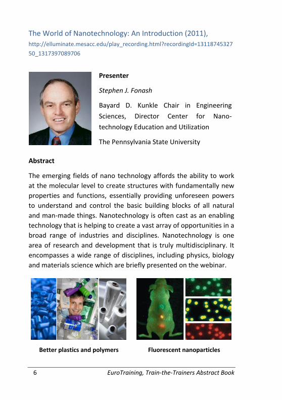
The World of Nanotechnology: An Introduction (2011),
http://elluminate.mesacc.edu/play_recording.html?recordingId=13118745327
50_1317397089706
Presenter
Stephen J. Fonash
Bayard D. Kunkle Chair in Engineering
Sciences, Director Center for Nano-
technology Education and Utilization
The Pennsylvania State University
Abstract
The emerging fields of nano technology affords the ability to work
at the molecular level to create structures with fundamentally new
properties and functions, essentially providing unforeseen powers
to understand and control the basic building blocks of all natural
and man-made things. Nanotechnology is often cast as an enabling
technology that is helping to create a vast array of opportunities in a
broad range of industries and disciplines. Nanotechnology is one
area of research and development that is truly multidisciplinary. It
encompasses a wide range of disciplines, including physics, biology
and materials science which are briefly presented on the webinar.
Better plastics and polymers
Fluorescent nanoparticles
EuroTraining, Train-the-Trainers Abstract Book 7
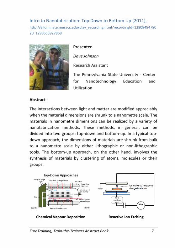
Intro to Nanofabrication: Top Down to Bottom Up (2011),
http://elluminate.mesacc.edu/play_recording.html?recordingId=12808494780
20_1298653927868
Presenter
Dave Johnson
Research Assistant
The Pennsylvania State University - Center
for Nanotechnology Education and
Utilization
Abstract
The interactions between light and matter are modified appreciably
when the material dimensions are shrunk to a nanometre scale. The
materials in nanometre dimensions can be realized by a variety of
nanofabrication methods. These methods, in general, can be
divided into two groups: top-down and bottom-up. In a typical top-
down approach, the dimensions of materials are shrunk from bulk
to a nanometre scale by either lithographic or non-lithographic
tools. The bottom-up approach, on the other hand, involves the
synthesis of materials by clustering of atoms, molecules or their
groups.
Chemical Vapour Deposition
Reactive Ion Etching
8 EuroTraining, Train-the-Trainers Abstract Book
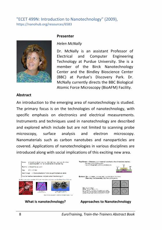
"ECET 499N: Introduction to Nanotechnology" (2009), https://nanohub.org/resources/6583
Presenter
Helen McNally
Dr. McNally is an assistant Professor of Electrical and Computer Engineering Technology at Purdue University. She is a member of the Birck Nanotechnology Center and the Bindley Bioscience Center (BBC) at Purdue’s Discovery Park. Dr. McNally currently directs the BBC Biological Atomic Force Microscopy (BioAFM) Facility.
Abstract
An introduction to the emerging area of nanotechnology is studied.
The primary focus is on the technologies of nanotechnology, with
specific emphasis on electronics and electrical measurements.
Instruments and techniques used in nanotechnology are described
and explored which include but are not limited to scanning probe
microscopy, surface analysis and electron microscopy.
Nanomaterials such as carbon nanotubes and nanoparticles are
covered. Applications of nanotechnologies in various disciplines are
introduced along with social implications of this exciting new area.
What is nanotechnology?
Approaches to Nanotechnology
EuroTraining, Train-the-Trainers Abstract Book 9
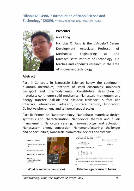
"Illinois ME 498NF: Introduction of Nano Science and Technology" (2009), https://nanohub.org/resources/7313
Presenter
Nick Fang
Nicholas X. Fang is the d’Arbeloff Career
Development Associate Professor of
Mechanical Engineering at the
Massachusetts Institute of Technology. He
teaches and conducts research in the area
of micro/nanotechnology.
Abstract
Part I: Concepts in Nanoscale Science; Below the continuum: quantum mechanics; Statistics of small ensembles: molecular transport and thermodynamics; Constitutive description of materials: continuum solid mechanics; Nanoscale momentum and energy transfer: ballistic and diffusive transport; Surface and interface interactions: adhesion, surface tension, lubrication; Collective phenomena and temporal-spatial scales.
Part II: Primer on Nanotechnology; Nanophase materials: design, synthesis and characterization; Nanodevice thermal and fluidic management; Nanoscale sensing, nanometrology and actuation; Nanosystem energy conversion; Nanomanufacturing: challenges and opportunities; Nanoscale biomimetic devices and systems
What is and why nanoscale?
Relative significance of forces
10 EuroTraining, Train-the-Trainers Abstract Book
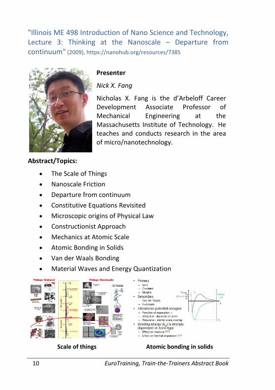
"Illinois ME 498 Introduction of Nano Science and Technology, Lecture 3: Thinking at the Nanoscale – Departure from continuum" (2009), https://nanohub.org/resources/7385
Presenter
Nick X. Fang
Nicholas X. Fang is the d’Arbeloff Career Development Associate Professor of Mechanical Engineering at the Massachusetts Institute of Technology. He teaches and conducts research in the area of micro/nanotechnology.
Abstract/Topics:
The Scale of Things
Nanoscale Friction
Departure from continuum
Constitutive Equations Revisited
Microscopic origins of Physical Law
Constructionist Approach
Mechanics at Atomic Scale
Atomic Bonding in Solids
Van der Waals Bonding
Material Waves and Energy Quantization
Scale of things
Atomic bonding in solids
EuroTraining, Train-the-Trainers Abstract Book 11
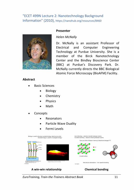
"ECET 499N Lecture 2: Nanotechnology Background Information" (2010), https://nanohub.org/resources/8460
Presenter
Helen McNally
Dr. McNally is an assistant Professor of Electrical and Computer Engineering Technology at Purdue University. She is a member of the Birck Nanotechnology Center and the Bindley Bioscience Center (BBC) at Purdue’s Discovery Park. Dr. McNally currently directs the BBC Biological Atomic Force Microscopy (BioAFM) Facility.
Abstract
Basic Sciences
Biology
Chemistry
Physics
Math
Concepts
Resonators
Particle Wave Duality
Fermi Levels
A win-win relationship
Chemical bonding
12 EuroTraining, Train-the-Trainers Abstract Book
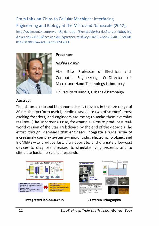
From Labs-on-Chips to Cellular Machines: Interfacing
Engineering and Biology at the Micro and Nanoscale (2012),
http://event.on24.com/eventRegistration/EventLobbyServlet?target=lobby.jsp
&eventid=544564&sessionid=1&partnerref=&key=E021373275E558E537AFDB
01C8607DF2&eventuserid=7796813
Presenter
Rashid Bashir
Abel Bliss Professor of Electrical and
Computer Engineering, Co-Director of
Micro- and Nano-Technology Laboratory
University of Illinois, Urbana-Champaign
Abstract
The lab-on-a-chip and bionanomachines (devices in the size range of 80 nm that perform useful, medical tasks) are two of science’s most exciting frontiers, and engineers are racing to make them everyday realities. (The Tricorder X Prize, for example, aims to produce a real-world version of the Star Trek device by the end of the decade.) The effort, though, demands that engineers integrate a wide array of increasingly complex systems—microfluidic, electronic, biologic, and BioMEMS—to produce fast, ultra-accurate, and ultimately low-cost devices to diagnose diseases, to simulate living systems, and to stimulate basic life-science research.
Integrated lab-on-a-chip
3D stereo lithography
EuroTraining, Train-the-Trainers Abstract Book 13
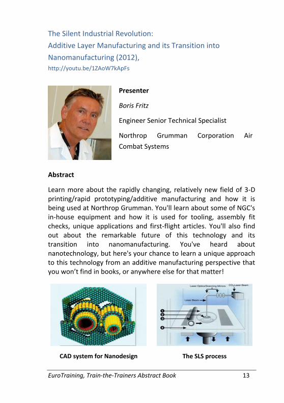
The Silent Industrial Revolution:
Additive Layer Manufacturing and its Transition into
Nanomanufacturing (2012),
http://youtu.be/1ZAoW7kApFs
Presenter
Boris Fritz
Engineer Senior Technical Specialist
Northrop Grumman Corporation Air
Combat Systems
Abstract
Learn more about the rapidly changing, relatively new field of 3-D printing/rapid prototyping/additive manufacturing and how it is being used at Northrop Grumman. You'll learn about some of NGC's in-house equipment and how it is used for tooling, assembly fit checks, unique applications and first-flight articles. You'll also find out about the remarkable future of this technology and its transition into nanomanufacturing. You've heard about nanotechnology, but here's your chance to learn a unique approach to this technology from an additive manufacturing perspective that you won’t find in books, or anywhere else for that matter!
CAD system for Nanodesign
The SLS process

14 EuroTraining, Train-the-Trainers Abstract Book

EuroTraining, Train-the-Trainers Abstract Book 15
MATERIALS PROPERTIES AND PERFORMANCE
16 EuroTraining, Train-the-Trainers Abstract Book
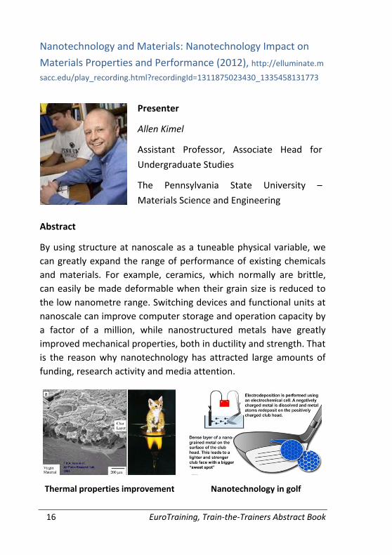
Nanotechnology and Materials: Nanotechnology Impact on
Materials Properties and Performance (2012), http://elluminate.m
sacc.edu/play_recording.html?recordingId=1311875023430_1335458131773
Presenter
Allen Kimel
Assistant Professor, Associate Head for
Undergraduate Studies
The Pennsylvania State University –
Materials Science and Engineering
Abstract
By using structure at nanoscale as a tuneable physical variable, we
can greatly expand the range of performance of existing chemicals
and materials. For example, ceramics, which normally are brittle,
can easily be made deformable when their grain size is reduced to
the low nanometre range. Switching devices and functional units at
nanoscale can improve computer storage and operation capacity by
a factor of a million, while nanostructured metals have greatly
improved mechanical properties, both in ductility and strength. That
is the reason why nanotechnology has attracted large amounts of
funding, research activity and media attention.
Thermal properties improvement
Nanotechnology in golf

EuroTraining, Train-the-Trainers Abstract Book 17
Thermal Energy at the Nanoscale (2013), https://nanohub.org/groups/u/spring2013_thermal_energy_at_the_nanoscale
Presenter
Timothy S. Fisher
He joined Purdue University’s School of Mechanical Engineering and Birck Nano-technology Center in 2002. His research has included studies of nanoscale heat transfer, coupled electro-thermal effects in electron emission and semiconductor devices, energy conversion and storage materials and devices, and related computational methods.
Abstract
Thermal Energy at the Nanoscale is a five-week online course that
develops a unified framework for understanding essential physics of
nanoscale thermal energy and its important applications, trends,
and directions. The course is taught at the level of a Purdue
graduate course for first-year students, but there are no admission
requirements and no need to travel to Purdue. The online course
can be taken from anywhere in the world from March through April
2013. Each week contains six 20-minute video lectures covering
essential physics, practical considerations, models for simulation,
and fundamental limits.
Week 1: Lattice Structure, Phonons, and Electrons (available free) L1.1: Introduction and Atomic Bonding L1.2: Mathematical Description of the Lattice L1.3: Lattice Vibrations and Phonons L1.4: Free Electrons L1.5: Example 1D Atomic Chain with a Diatomic Basis L1.6: Week 1 Wrap Up
18 EuroTraining, Train-the-Trainers Abstract Book
From Atoms to Materials: Predictive Theory and Simulations (2010), https://nanohub.org/groups/u/spring2013_from_atoms_to_materials
Presenter
Alejandro Strachan
He is an associate professor of materials engineering at Purdue University and the deputy director of NNSA’s Center for the Prediction of Reliability, Integrity and Survivability of Microsystems. His research focuses on the development of predictive atomistic and molecular simulation methodologies to describe materials from first principles, their application to problems of technological importance and quantification of associated uncertainties.
Abstract
From Atoms to Materials: Predictive Theory and Simulations is a
five-week online course that develops a unified framework for
understanding essential physics that govern materials at atomic
scales and relate these processes to the macroscopic world. The
course will cover important applications, trends, and directions. The
course is taught at the level of a Purdue graduate course for first-
year students, but there are no admission requirements and no
need to travel to Purdue. The online course can be taken from
anywhere in the world from May 13 through June 14, 2013. Each
week contains six 20-minute video lectures.
EuroTraining, Train-the-Trainers Abstract Book 19
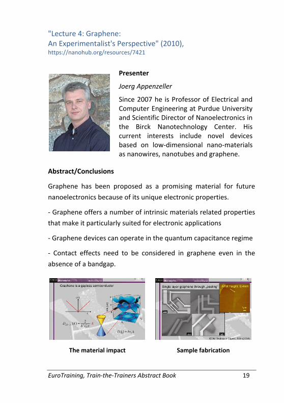
"Lecture 4: Graphene: An Experimentalist's Perspective" (2010), https://nanohub.org/resources/7421
Presenter
Joerg Appenzeller
Since 2007 he is Professor of Electrical and Computer Engineering at Purdue University and Scientific Director of Nanoelectronics in the Birck Nanotechnology Center. His current interests include novel devices based on low-dimensional nano-materials as nanowires, nanotubes and graphene.
Abstract/Conclusions
Graphene has been proposed as a promising material for future
nanoelectronics because of its unique electronic properties.
- Graphene offers a number of intrinsic materials related properties
that make it particularly suited for electronic applications
- Graphene devices can operate in the quantum capacitance regime
- Contact effects need to be considered in graphene even in the
absence of a bandgap.
The material impact
Sample fabrication

20 EuroTraining, Train-the-Trainers Abstract Book

EuroTraining, Train-the-Trainers Abstract Book 21
CHARACTERISATION TECHNIQUES

22 EuroTraining, Train-the-Trainers Abstract Book
"ECET 499N Lecture 12: Scanning Probe Microscopy Applications (in Neuroscience and Beyond)" (2010), https://nanohub.org/resources/8837
Presenter
Helen McNally
Dr. McNally is an assistant Professor of Electrical and Computer Engineering Technology at Purdue University. She is a member of the Birck Nanotechnology Center and the Bindley Bioscience Center (BBC) at Purdue’s Discovery Park. Dr. McNally currently directs the BBC Biological Atomic Force Microscopy (BioAFM) Facility.
Abstract
Scanning Probe Microscopy (SPM)
Scanning Tunneling Microscopy – Rohrer and Binnig 1982
Atomic Force Microscopy (AFM/SFM) – Binnig et al 1986
Resolution:
Optical: 200nm
AFM: atomic resolution possible, depending on tip dimension, detection system, operating conditions & controls
Measurement capabilities: topography and material characteristics
Operating conditions: vacuum, air (gas), liquid, and hyperbaric
Growing process
Z-projections
EuroTraining, Train-the-Trainers Abstract Book 23
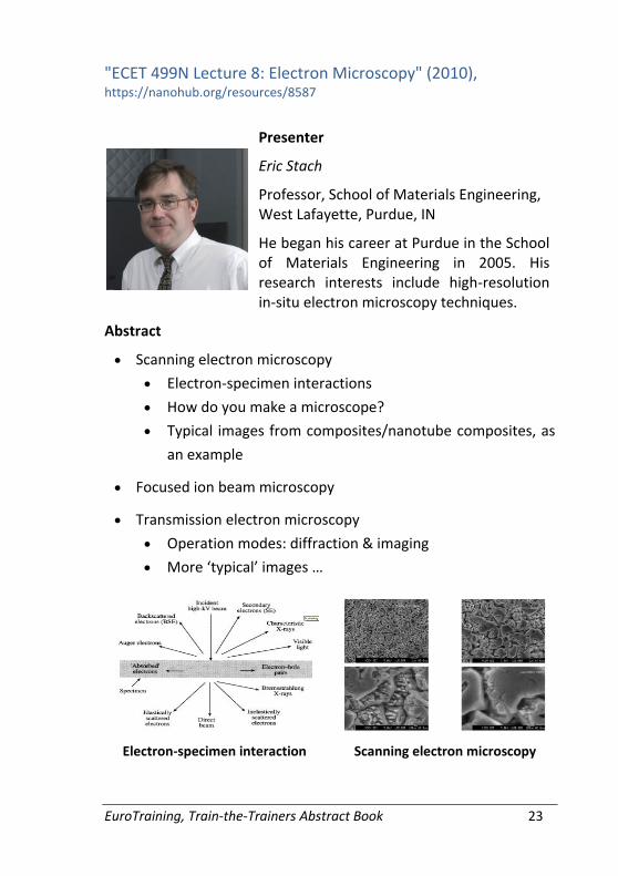
"ECET 499N Lecture 8: Electron Microscopy" (2010), https://nanohub.org/resources/8587
Presenter
Eric Stach
Professor, School of Materials Engineering, West Lafayette, Purdue, IN
He began his career at Purdue in the School of Materials Engineering in 2005. His research interests include high-resolution in-situ electron microscopy techniques.
Abstract
Scanning electron microscopy
Electron-specimen interactions
How do you make a microscope?
Typical images from composites/nanotube composites, as
an example
Focused ion beam microscopy
Transmission electron microscopy
Operation modes: diffraction & imaging
More ‘typical’ images …
Electron-specimen interaction
Scanning electron microscopy
24 EuroTraining, Train-the-Trainers Abstract Book
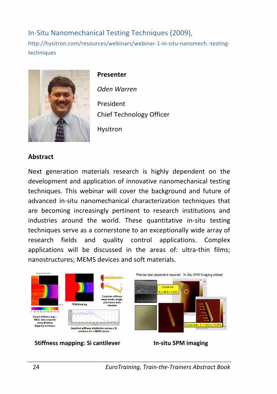
In-Situ Nanomechanical Testing Techniques (2009),
http://hysitron.com/resources/webinars/webinar-1-in-situ-nanomech.-testing-
techniques
Presenter
Oden Warren
President
Chief Technology Officer
Hysitron
Abstract
Next generation materials research is highly dependent on the
development and application of innovative nanomechanical testing
techniques. This webinar will cover the background and future of
advanced in-situ nanomechanical characterization techniques that
are becoming increasingly pertinent to research institutions and
industries around the world. These quantitative in-situ testing
techniques serve as a cornerstone to an exceptionally wide array of
research fields and quality control applications. Complex
applications will be discussed in the areas of: ultra-thin films;
nanostructures; MEMS devices and soft materials.
Stiffness mapping: Si cantilever
In-situ SPM imaging
EuroTraining, Train-the-Trainers Abstract Book 25
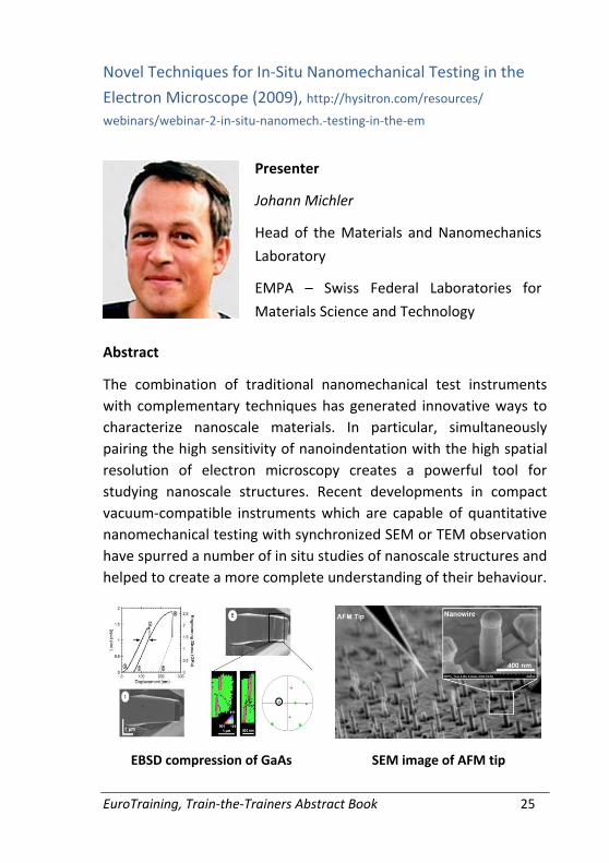
Novel Techniques for In-Situ Nanomechanical Testing in the
Electron Microscope (2009), http://hysitron.com/resources/
webinars/webinar-2-in-situ-nanomech.-testing-in-the-em
Presenter
Johann Michler
Head of the Materials and Nanomechanics
Laboratory
EMPA – Swiss Federal Laboratories for
Materials Science and Technology
Abstract
The combination of traditional nanomechanical test instruments
with complementary techniques has generated innovative ways to
characterize nanoscale materials. In particular, simultaneously
pairing the high sensitivity of nanoindentation with the high spatial
resolution of electron microscopy creates a powerful tool for
studying nanoscale structures. Recent developments in compact
vacuum-compatible instruments which are capable of quantitative
nanomechanical testing with synchronized SEM or TEM observation
have spurred a number of in situ studies of nanoscale structures and
helped to create a more complete understanding of their behaviour.
EBSD compression of GaAs
SEM image of AFM tip
26 EuroTraining, Train-the-Trainers Abstract Book
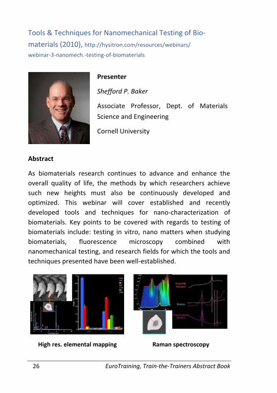
Tools & Techniques for Nanomechanical Testing of Bio-
materials (2010), http://hysitron.com/resources/webinars/
webinar-3-nanomech.-testing-of-biomaterials
Presenter
Shefford P. Baker
Associate Professor, Dept. of Materials
Science and Engineering
Cornell University
Abstract
As biomaterials research continues to advance and enhance the
overall quality of life, the methods by which researchers achieve
such new heights must also be continuously developed and
optimized. This webinar will cover established and recently
developed tools and techniques for nano-characterization of
biomaterials. Key points to be covered with regards to testing of
biomaterials include: testing in vitro, nano matters when studying
biomaterials, fluorescence microscopy combined with
nanomechanical testing, and research fields for which the tools and
techniques presented have been well-established.
High res. elemental mapping
Raman spectroscopy

EuroTraining, Train-the-Trainers Abstract Book 27
Nanomechanical Characterization in Irradiated Materials
(2011), http://www.hysitron.com/resources/webinars/webinar-7-irradiated-
materials
Presenter
Peter Hosemann
Assistant Professor, Department of Nuclear
Engineering
University of California-Berkeley
Abstract
The world continues to increase its demand for innovation in energy
research, which is supported by increased government spending on
energy and a rising number of worldwide researchers focusing
efforts in this area. Many energy-related research initiatives
inherently require small-scale material analysis due to the micro-
and nano-scale feature sizes in new and improved materials for
energy innovation. Key energy-related topics include:
photovoltaics, solar cells, batteries, fuel cells, lightweight materials
(steels, aluminium, alloys, etc.), fuel rods, nuclear materials, and
irradiated materials.
Cross-section material testing
SEM image of diffusion bonding
28 EuroTraining, Train-the-Trainers Abstract Book
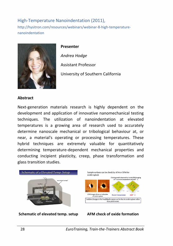
High-Temperature Nanoindentation (2011),
http://hysitron.com/resources/webinars/webinar-8-high-temperature-
nanoindentation
Presenter
Andrea Hodge
Assistant Professor
University of Southern California
Abstract
Next-generation materials research is highly dependent on the
development and application of innovative nanomechanical testing
techniques. The utilization of nanoindentation at elevated
temperatures is a growing area of research used to accurately
determine nanoscale mechanical or tribological behaviour at, or
near, a material's operating or processing temperatures. These
hybrid techniques are extremely valuable for quantitatively
determining temperature-dependent mechanical properties and
conducting incipient plasticity, creep, phase transformation and
glass transition studies.
Schematic of elevated temp. setup
AFM check of oxide formation
EuroTraining, Train-the-Trainers Abstract Book 29
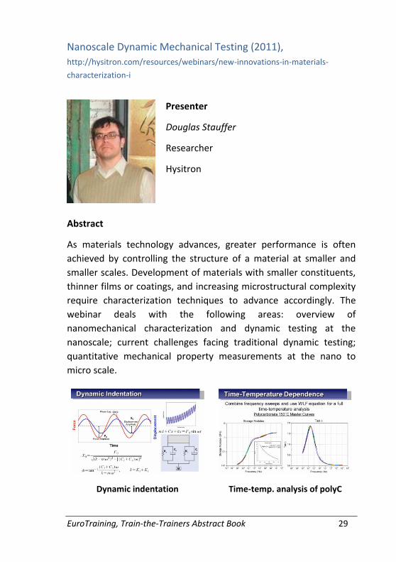
Nanoscale Dynamic Mechanical Testing (2011),
http://hysitron.com/resources/webinars/new-innovations-in-materials-
characterization-i
Presenter
Douglas Stauffer
Researcher
Hysitron
Abstract
As materials technology advances, greater performance is often
achieved by controlling the structure of a material at smaller and
smaller scales. Development of materials with smaller constituents,
thinner films or coatings, and increasing microstructural complexity
require characterization techniques to advance accordingly. The
webinar deals with the following areas: overview of
nanomechanical characterization and dynamic testing at the
nanoscale; current challenges facing traditional dynamic testing;
quantitative mechanical property measurements at the nano to
micro scale.
Dynamic indentation
Time-temp. analysis of polyC
30 EuroTraining, Train-the-Trainers Abstract Book
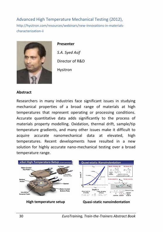
Advanced High Temperature Mechanical Testing (2012),
http://hysitron.com/resources/webinars/new-innovations-in-materials-
characterization-ii
Presenter
S.A. Syed Asif
Director of R&D
Hysitron
Abstract
Researchers in many industries face significant issues in studying
mechanical properties of a broad range of materials at high
temperatures that represent operating or processing conditions.
Accurate quantitative data adds significantly to the process of
materials property modelling. Oxidation, thermal drift, sample/tip
temperature gradients, and many other issues make it difficult to
acquire accurate nanomechanical data at elevated, high
temperatures. Recent developments have resulted in a new
solution for highly accurate nano-mechanical testing over a broad
temperature range.
High temperature setup
Quasi-static nanoindentation
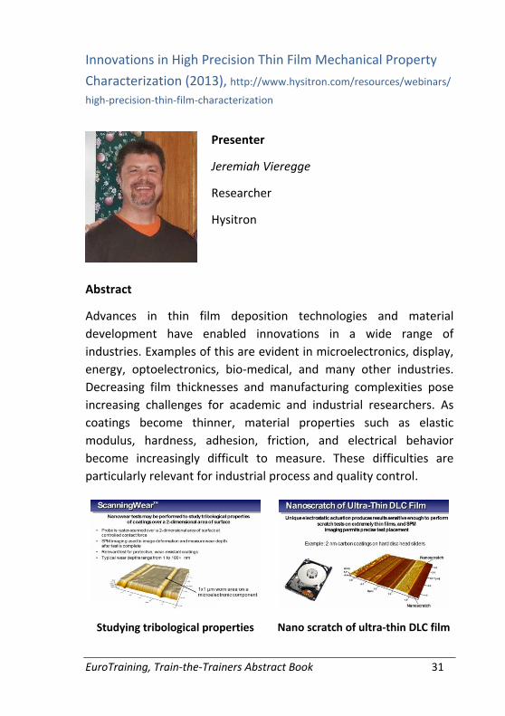
EuroTraining, Train-the-Trainers Abstract Book 31
Innovations in High Precision Thin Film Mechanical Property
Characterization (2013), http://www.hysitron.com/resources/webinars/
high-precision-thin-film-characterization
Presenter
Jeremiah Vieregge
Researcher
Hysitron
Abstract
Advances in thin film deposition technologies and material
development have enabled innovations in a wide range of
industries. Examples of this are evident in microelectronics, display,
energy, optoelectronics, bio-medical, and many other industries.
Decreasing film thicknesses and manufacturing complexities pose
increasing challenges for academic and industrial researchers. As
coatings become thinner, material properties such as elastic
modulus, hardness, adhesion, friction, and electrical behavior
become increasingly difficult to measure. These difficulties are
particularly relevant for industrial process and quality control.
Studying tribological properties
Nano scratch of ultra-thin DLC film
32 EuroTraining, Train-the-Trainers Abstract Book
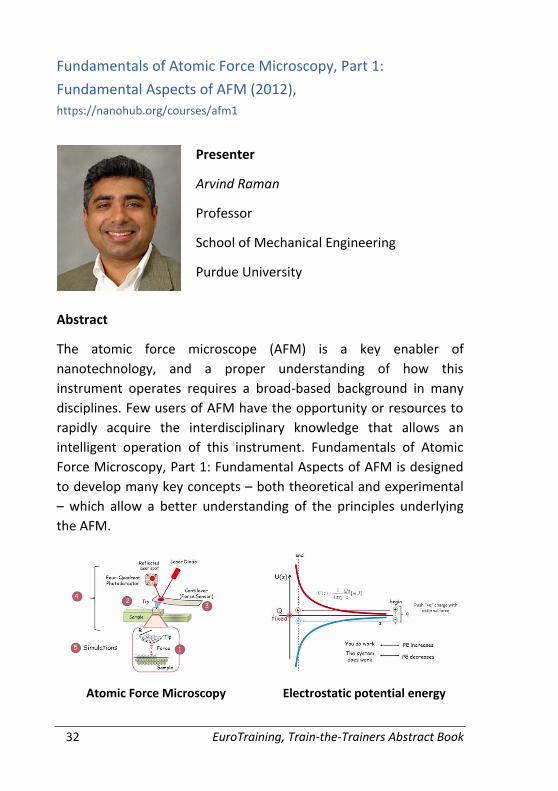
Fundamentals of Atomic Force Microscopy, Part 1:
Fundamental Aspects of AFM (2012),
https://nanohub.org/courses/afm1
Presenter
Arvind Raman
Professor
School of Mechanical Engineering
Purdue University
Abstract
The atomic force microscope (AFM) is a key enabler of
nanotechnology, and a proper understanding of how this
instrument operates requires a broad-based background in many
disciplines. Few users of AFM have the opportunity or resources to
rapidly acquire the interdisciplinary knowledge that allows an
intelligent operation of this instrument. Fundamentals of Atomic
Force Microscopy, Part 1: Fundamental Aspects of AFM is designed
to develop many key concepts – both theoretical and experimental
– which allow a better understanding of the principles underlying
the AFM.
Atomic Force Microscopy
Electrostatic potential energy
EuroTraining, Train-the-Trainers Abstract Book 33
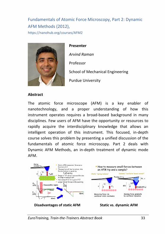
Fundamentals of Atomic Force Microscopy, Part 2: Dynamic
AFM Methods (2012),
https://nanohub.org/courses/AFM2
Presenter
Arvind Raman
Professor
School of Mechanical Engineering
Purdue University
Abstract
The atomic force microscope (AFM) is a key enabler of
nanotechnology, and a proper understanding of how this
instrument operates requires a broad-based background in many
disciplines. Few users of AFM have the opportunity or resources to
rapidly acquire the interdisciplinary knowledge that allows an
intelligent operation of this instrument. This focused, in-depth
course solves this problem by presenting a unified discussion of the
fundamentals of atomic force microscopy. Part 2 deals with
Dynamic AFM Methods, an in-depth treatment of dynamic mode
AFM.
Disadvantages of static AFM
Static vs. dynamic AFM

34 EuroTraining, Train-the-Trainers Abstract Book
EuroTraining, Train-the-Trainers Abstract Book 35
NANOELECTRONICS AND OTHER APPLICATIONS
36 EuroTraining, Train-the-Trainers Abstract Book
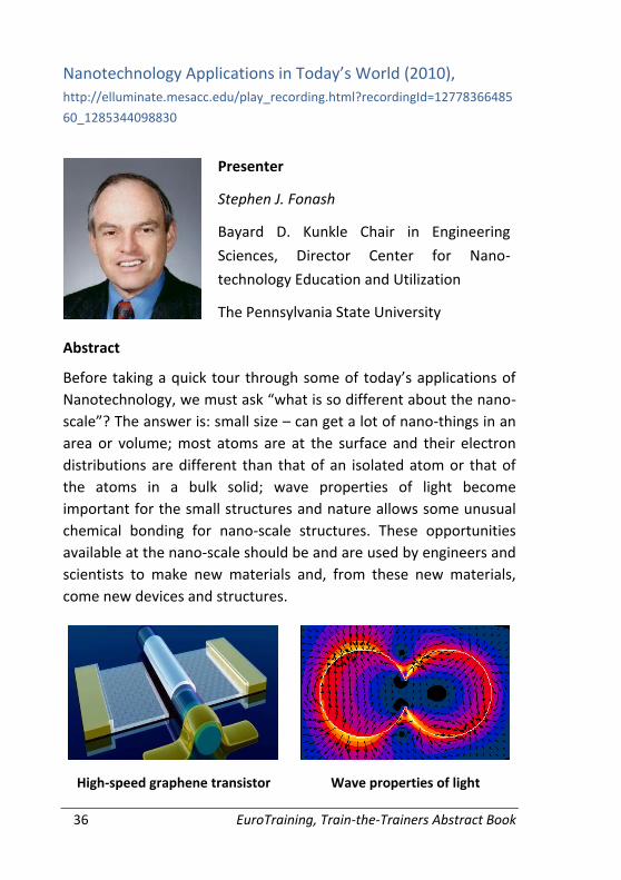
Nanotechnology Applications in Today’s World (2010),
http://elluminate.mesacc.edu/play_recording.html?recordingId=12778366485
60_1285344098830
Presenter
Stephen J. Fonash
Bayard D. Kunkle Chair in Engineering
Sciences, Director Center for Nano-
technology Education and Utilization
The Pennsylvania State University
Abstract
Before taking a quick tour through some of today’s applications of
Nanotechnology, we must ask “what is so different about the nano-
scale”? The answer is: small size – can get a lot of nano-things in an
area or volume; most atoms are at the surface and their electron
distributions are different than that of an isolated atom or that of
the atoms in a bulk solid; wave properties of light become
important for the small structures and nature allows some unusual
chemical bonding for nano-scale structures. These opportunities
available at the nano-scale should be and are used by engineers and
scientists to make new materials and, from these new materials,
come new devices and structures.
High-speed graphene transistor
Wave properties of light
EuroTraining, Train-the-Trainers Abstract Book 37
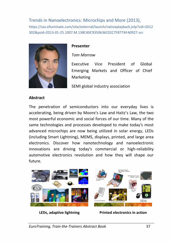
Trends in Nanoelectronics: Microchips and More (2013),
https://sas.elluminate.com/site/external/launch/nativeplayback.jnlp?sid=2012
302&psid=2013-01-25.1007.M.13BC40C9350636C02C7F877AFA0927.vcr
Presenter
Tom Morrow
Executive Vice President of Global
Emerging Markets and Officer of Chief
Marketing
SEMI global industry association
Abstract
The penetration of semiconductors into our everyday lives is
accelerating, being driven by Moore's Law and Haitz’s Law, the two
most powerful economic and social forces of our time. Many of the
same technologies and processes developed to make today's most
advanced microchips are now being utilized in solar energy, LEDs
(including Smart Lightning), MEMS, displays, printed, and large area
electronics. Discover how nanotechnology and nanoelectronic
innovations are driving today's commercial or high-reliability
automotive electronics revolution and how they will shape our
future.
LEDs, adaptive lightning
Printed electronics in action
38 EuroTraining, Train-the-Trainers Abstract Book
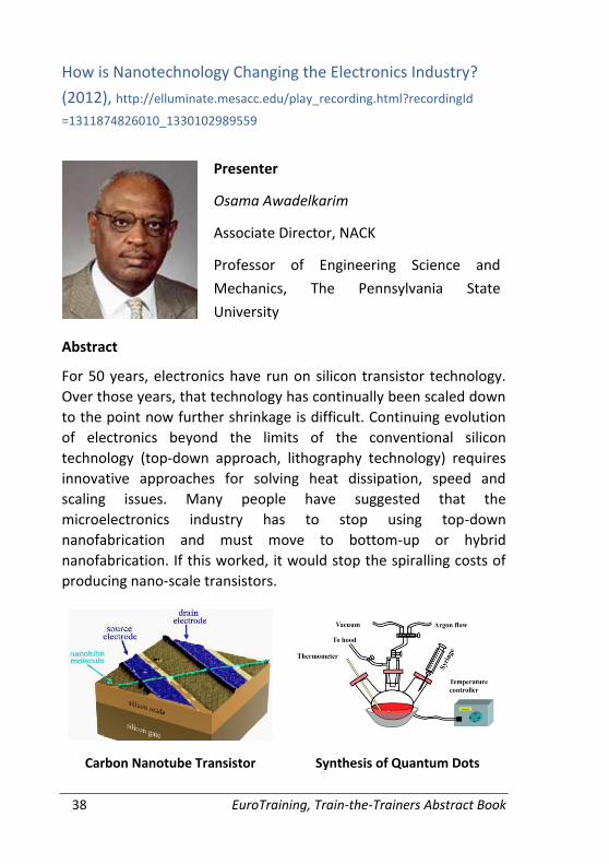
How is Nanotechnology Changing the Electronics Industry?
(2012), http://elluminate.mesacc.edu/play_recording.html?recordingId
=1311874826010_1330102989559
Presenter
Osama Awadelkarim
Associate Director, NACK
Professor of Engineering Science and
Mechanics, The Pennsylvania State
University
Abstract
For 50 years, electronics have run on silicon transistor technology.
Over those years, that technology has continually been scaled down
to the point now further shrinkage is difficult. Continuing evolution
of electronics beyond the limits of the conventional silicon
technology (top-down approach, lithography technology) requires
innovative approaches for solving heat dissipation, speed and
scaling issues. Many people have suggested that the
microelectronics industry has to stop using top-down
nanofabrication and must move to bottom-up or hybrid
nanofabrication. If this worked, it would stop the spiralling costs of
producing nano-scale transistors.
Carbon Nanotube Transistor
Synthesis of Quantum Dots
EuroTraining, Train-the-Trainers Abstract Book 39
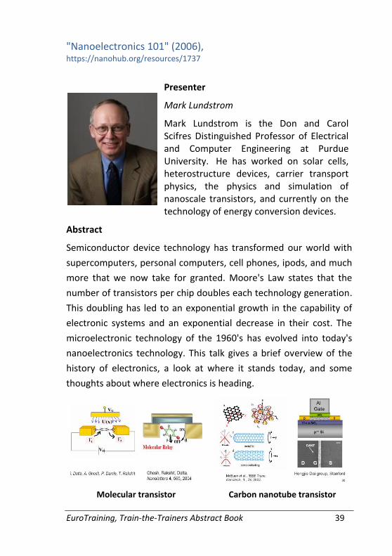
"Nanoelectronics 101" (2006), https://nanohub.org/resources/1737
Presenter
Mark Lundstrom
Mark Lundstrom is the Don and Carol Scifres Distinguished Professor of Electrical and Computer Engineering at Purdue University. He has worked on solar cells, heterostructure devices, carrier transport physics, the physics and simulation of nanoscale transistors, and currently on the technology of energy conversion devices.
Abstract
Semiconductor device technology has transformed our world with
supercomputers, personal computers, cell phones, ipods, and much
more that we now take for granted. Moore's Law states that the
number of transistors per chip doubles each technology generation.
This doubling has led to an exponential growth in the capability of
electronic systems and an exponential decrease in their cost. The
microelectronic technology of the 1960's has evolved into today's
nanoelectronics technology. This talk gives a brief overview of the
history of electronics, a look at where it stands today, and some
thoughts about where electronics is heading.
Molecular transistor
Carbon nanotube transistor
40 EuroTraining, Train-the-Trainers Abstract Book
"ECET 499N Lecture 3: Nanoelectronics 1" (2010), https://nanohub.org/resources/8473
Presenter
Helen McNally
Dr. McNally is an assistant Professor of Electrical and Computer Engineering Technology at Purdue University. She is a member of the Birck Nanotechnology Center and the Bindley Bioscience Center (BBC) at Purdue’s Discovery Park. Dr. McNally currently directs the BBC Biological Atomic Force Microscopy (BioAFM) Facility.
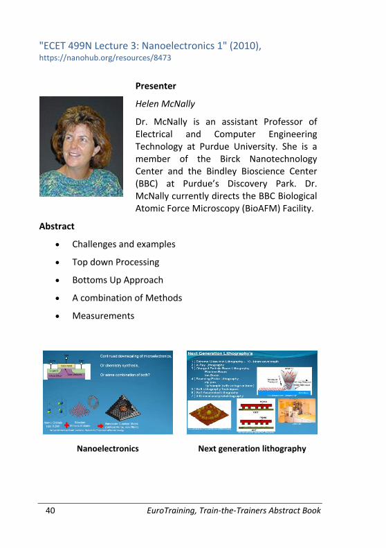
Abstract
Challenges and examples
Top down Processing
Bottoms Up Approach
A combination of Methods
Measurements
Nanoelectronics
Next generation lithography
EuroTraining, Train-the-Trainers Abstract Book 41
"ECET 499N Lecture 4: Nanoelectronics 2" (2010) https://nanohub.org/resources/8474
Presenter
Helen McNally
Dr. McNally is an assistant Professor of Electrical and Computer Engineering Technology at Purdue University. She is a member of the Birck Nanotechnology Center and the Bindley Bioscience Center (BBC) at Purdue’s Discovery Park. Dr. McNally currently directs the BBC Biological Atomic Force Microscopy (BioAFM) Facility.
Abstract
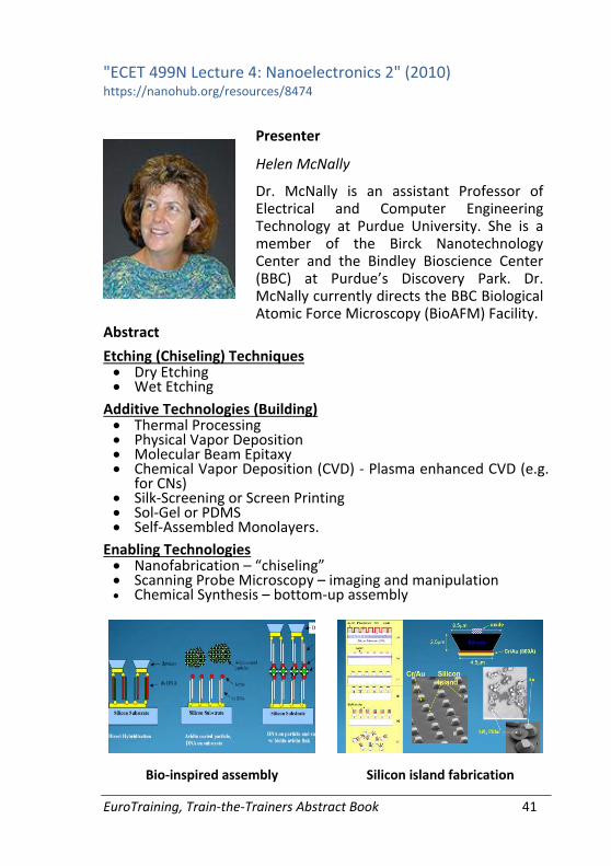
Etching (Chiseling) Techniques Dry Etching Wet Etching
Additive Technologies (Building) Thermal Processing Physical Vapor Deposition Molecular Beam Epitaxy Chemical Vapor Deposition (CVD) - Plasma enhanced CVD (e.g.
for CNs) Silk-Screening or Screen Printing Sol-Gel or PDMS Self-Assembled Monolayers.
Enabling Technologies Nanofabrication – “chiseling” Scanning Probe Microscopy – imaging and manipulation Chemical Synthesis – bottom-up assembly
Bio-inspired assembly
Silicon island fabrication
42 EuroTraining, Train-the-Trainers Abstract Book
"ECET 499N Lecture 5: Nanoelectronics 3" (2010) https://nanohub.org/resources/8475
Presenter
Helen McNally
Dr. McNally is an assistant Professor of Electrical and Computer Engineering Technology at Purdue University. She is a member of the Birck Nanotechnology Center and the Bindley Bioscience Center (BBC) at Purdue’s Discovery Park. Dr. McNally currently directs the BBC Biological Atomic Force Microscopy (BioAFM) Facility.
Abstract
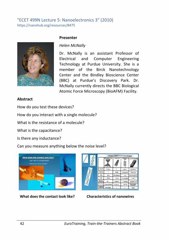
How do you test these devices?
How do you interact with a single molecule?
What is the resistance of a molecule?
What is the capacitance?
Is there any inductance?
Can you measure anything below the noise level?
What does the contact look like?
Characteristics of nanowires
EuroTraining, Train-the-Trainers Abstract Book 43
"ECET 499N: Nanoelectronics" (2009),
https://nanohub.org/resources/6580
Presenter
Supriyo Datta
Professor
Supriyo Datta is the Thomas Duncan
Distinguished Professor in the School of
Electrical and Computer Engineering.
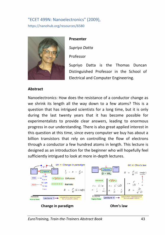
Abstract
Nanoelectronics: How does the resistance of a conductor change as
we shrink its length all the way down to a few atoms? This is a
question that has intrigued scientists for a long time, but it is only
during the last twenty years that it has become possible for
experimentalists to provide clear answers, leading to enormous
progress in our understanding. There is also great applied interest in
this question at this time, since every computer we buy has about a
billion transistors that rely on controlling the flow of electrons
through a conductor a few hundred atoms in length. This lecture is
designed as an introduction for the beginner who will hopefully feel
sufficiently intrigued to look at more in-depth lectures.
Change in paradigm
Ohm’s law
44 EuroTraining, Train-the-Trainers Abstract Book
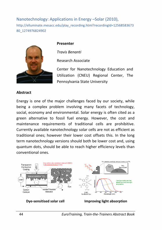
Nanotechnology: Applications in Energy –Solar (2010),
http://elluminate.mesacc.edu/play_recording.html?recordingId=12568583673
80_1274976824902
Presenter
Travis Benanti
Research Associate
Center for Nanotechnology Education and
Utilization (CNEU) Regional Center, The
Pennsylvania State University
Abstract
Energy is one of the major challenges faced by our society, while
being a complex problem involving many facets of technology,
social, economy and environmental. Solar energy is often cited as a
green alternative to fossil fuel energy. However, the cost and
maintenance requirements of traditional cells are prohibitive.
Currently available nanotechnology solar cells are not as efficient as
traditional ones; however their lower cost offsets this. In the long
term nanotechnology versions should both be lower cost and, using
quantum dots, should be able to reach higher efficiency levels than
conventional ones.
Dye-sensitised solar cell
Improving light absorption
EuroTraining, Train-the-Trainers Abstract Book 45
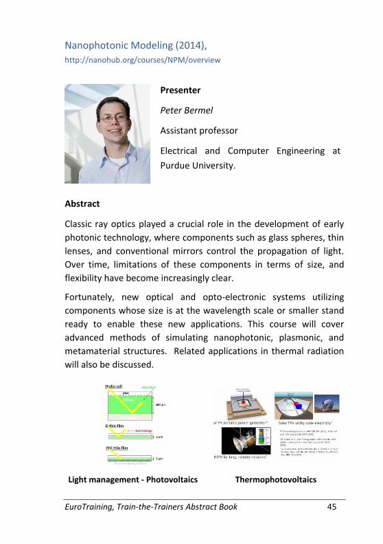
Nanophotonic Modeling (2014),
http://nanohub.org/courses/NPM/overview
Presenter
Peter Bermel
Assistant professor
Electrical and Computer Engineering at
Purdue University.
Abstract
Classic ray optics played a crucial role in the development of early
photonic technology, where components such as glass spheres, thin
lenses, and conventional mirrors control the propagation of light.
Over time, limitations of these components in terms of size, and
flexibility have become increasingly clear.
Fortunately, new optical and opto-electronic systems utilizing
components whose size is at the wavelength scale or smaller stand
ready to enable these new applications. This course will cover
advanced methods of simulating nanophotonic, plasmonic, and
metamaterial structures. Related applications in thermal radiation
will also be discussed.
Light management - Photovoltaics
Thermophotovoltaics
46 EuroTraining, Train-the-Trainers Abstract Book
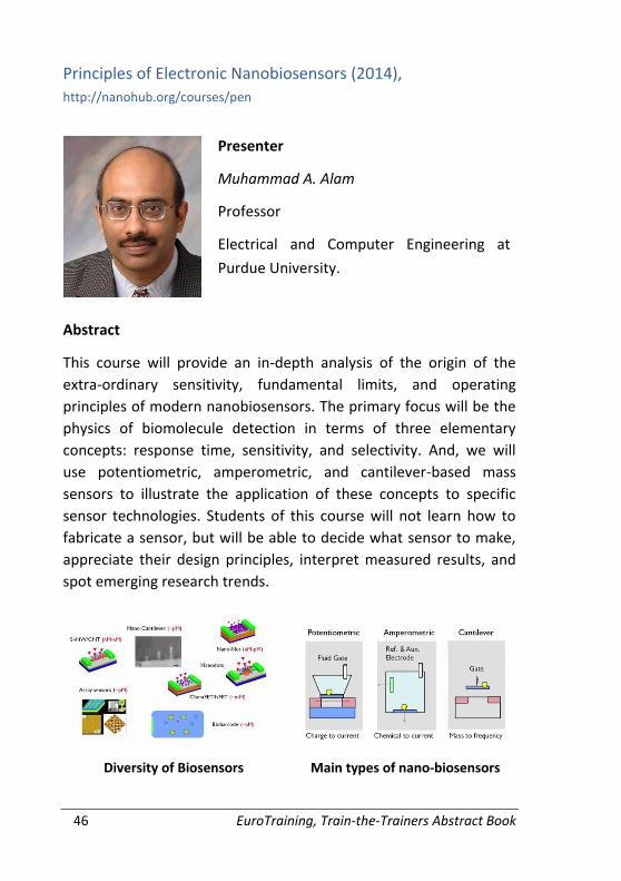
Principles of Electronic Nanobiosensors (2014),
http://nanohub.org/courses/pen
Presenter
Muhammad A. Alam
Professor
Electrical and Computer Engineering at
Purdue University.
Abstract
This course will provide an in-depth analysis of the origin of the
extra-ordinary sensitivity, fundamental limits, and operating
principles of modern nanobiosensors. The primary focus will be the
physics of biomolecule detection in terms of three elementary
concepts: response time, sensitivity, and selectivity. And, we will
use potentiometric, amperometric, and cantilever-based mass
sensors to illustrate the application of these concepts to specific
sensor technologies. Students of this course will not learn how to
fabricate a sensor, but will be able to decide what sensor to make,
appreciate their design principles, interpret measured results, and
spot emerging research trends.
Diversity of Biosensors
Main types of nano-biosensors
EuroTraining, Train-the-Trainers Abstract Book 47
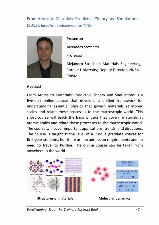
From Atoms to Materials: Predictive Theory and Simulations
(2013), http://nanohub.org/courses/FATM
Presenter
Alejandro Strachan
Professor
Alejandro Strachan: Materials Engineering,
Purdue University; Deputy Director, NNSA -
PRISM
Abstract
From Atoms to Materials: Predictive Theory and Simulations is a
five-unit online course that develops a unified framework for
understanding essential physics that govern materials at atomic
scales and relate these processes to the macroscopic world. This
short course will teach the basic physics that govern materials at
atomic scales and relate these processes to the macroscopic world.
The course will cover important applications, trends, and directions.
The course is taught at the level of a Purdue graduate course for
first-year students, but there are no admission requirements and no
need to travel to Purdue. The online course can be taken from
anywhere in the world.
Structures of materials
Molecular dynamics
48 EuroTraining, Train-the-Trainers Abstract Book
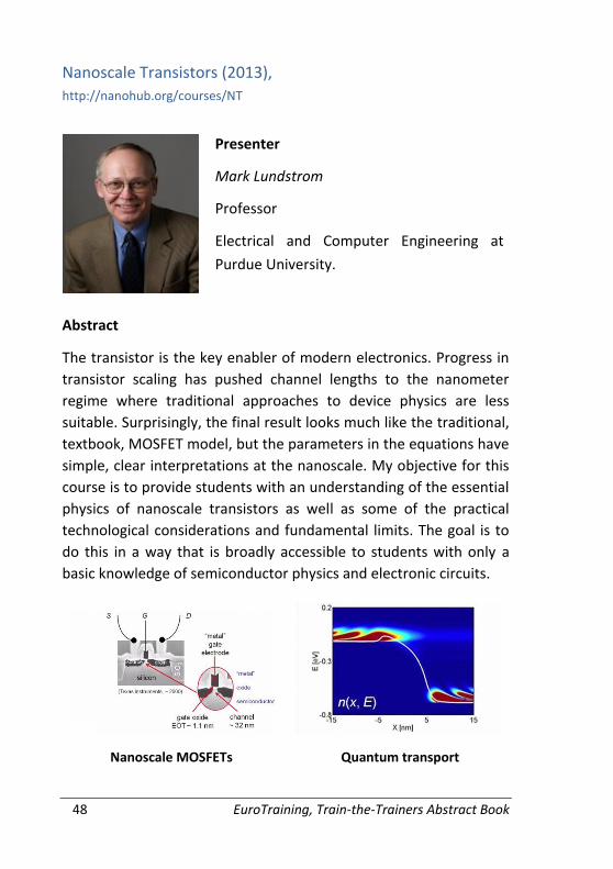
Nanoscale Transistors (2013),
http://nanohub.org/courses/NT
Presenter
Mark Lundstrom
Professor
Electrical and Computer Engineering at
Purdue University.
Abstract
The transistor is the key enabler of modern electronics. Progress in
transistor scaling has pushed channel lengths to the nanometer
regime where traditional approaches to device physics are less
suitable. Surprisingly, the final result looks much like the traditional,
textbook, MOSFET model, but the parameters in the equations have
simple, clear interpretations at the nanoscale. My objective for this
course is to provide students with an understanding of the essential
physics of nanoscale transistors as well as some of the practical
technological considerations and fundamental limits. The goal is to
do this in a way that is broadly accessible to students with only a
basic knowledge of semiconductor physics and electronic circuits.
Nanoscale MOSFETs
Quantum transport
EuroTraining, Train-the-Trainers Abstract Book 49
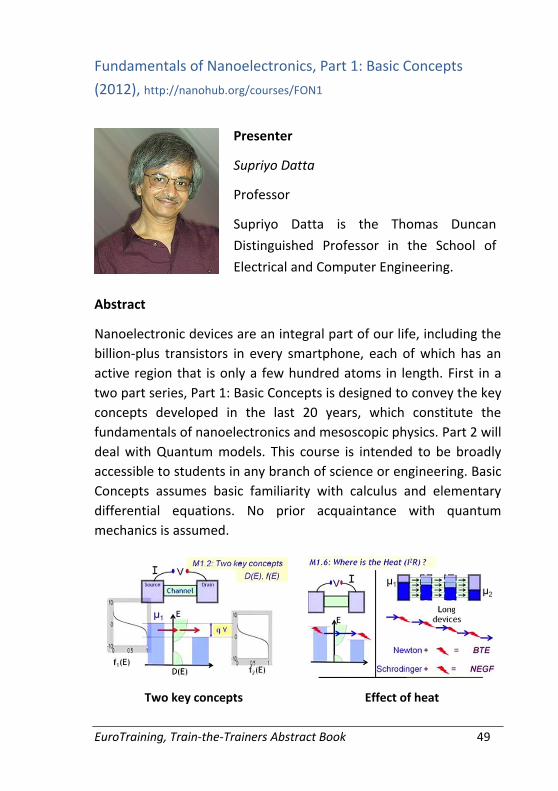
Fundamentals of Nanoelectronics, Part 1: Basic Concepts
(2012), http://nanohub.org/courses/FON1
Presenter
Supriyo Datta
Professor
Supriyo Datta is the Thomas Duncan
Distinguished Professor in the School of
Electrical and Computer Engineering.
Abstract
Nanoelectronic devices are an integral part of our life, including the
billion-plus transistors in every smartphone, each of which has an
active region that is only a few hundred atoms in length. First in a
two part series, Part 1: Basic Concepts is designed to convey the key
concepts developed in the last 20 years, which constitute the
fundamentals of nanoelectronics and mesoscopic physics. Part 2 will
deal with Quantum models. This course is intended to be broadly
accessible to students in any branch of science or engineering. Basic
Concepts assumes basic familiarity with calculus and elementary
differential equations. No prior acquaintance with quantum
mechanics is assumed.
Two key concepts
Effect of heat
50 EuroTraining, Train-the-Trainers Abstract Book
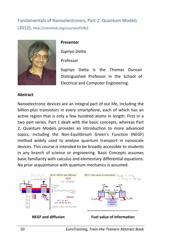
Fundamentals of Nanoelectronics, Part 2: Quantum Models
(2012), http://nanohub.org/courses/FON2
Presenter
Supriyo Datta
Professor
Supriyo Datta is the Thomas Duncan
Distinguished Professor in the School of
Electrical and Computer Engineering.
Abstract
Nanoelectronic devices are an integral part of our life, including the
billion-plus transistors in every smartphone, each of which has an
active region that is only a few hundred atoms in length. First in a
two part series, Part 1 dealt with the basic concepts, whereas Part
2, Quantum Models provides an introduction to more advanced
topics, including the Non-Equilibrium Green’s Function (NEGF)
method widely used to analyse quantum transport in nanoscale
devices. This course is intended to be broadly accessible to students
in any branch of science or engineering. Basic Concepts assumes
basic familiarity with calculus and elementary differential equations.
No prior acquaintance with quantum mechanics is assumed.
NEGF and diffusion
Fuel value of information

EuroTraining, Train-the-Trainers Abstract Book 51

52 EuroTraining, Train-the-Trainers Abstract Book
EuroTraining, Train-the-Trainers Abstract Book 53
USEFUL TOOLS
54 EuroTraining, Train-the-Trainers Abstract Book
Nanotechnology Demos and Simulations (2013),
https://sas.elluminate.com/site/external/launch/nativeplayback.jnlp?sid=2012
302&psid=2013-02-22.1012.M.EC234DFC079F0F5B83A1B62B10204D.vcr
Presenter
Michael Lesiecki
Director
Maricopa Advanced Technology Education
Center (MATEC) at the Maricopa
Community Colleges
Abstract
To engage today’s learners we need to present content and
information in different ways and to provide multiple means of
engagement. Sometimes, a system is too complex and hard to
visualize, analyse and explain it or it is variable with respect to time
or process and has multiple inter-dependent variables. And
sometimes… you just want to show something in a different way.
The possibilities of multimedia are so diverse that it would be
unfortunate to ignore it since one can present animations,
interactives, videos and can do simple and complex simulations,
emulations. The presentation shows how to incorporate these visual
tools to expose students to nanotechnology concepts.
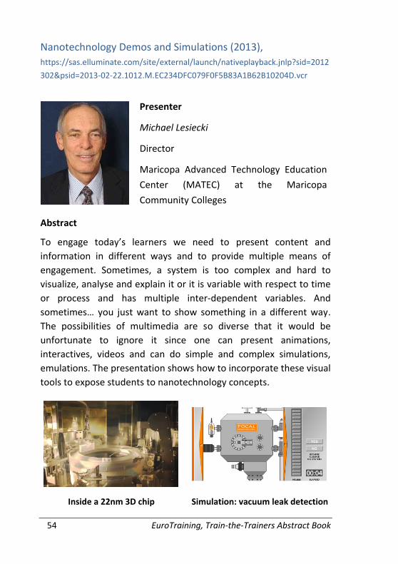
Inside a 22nm 3D chip
Simulation: vacuum leak detection
EuroTraining, Train-the-Trainers Abstract Book 55
Chanaka Suranjith Rupasinghe; Mufthas Rasikim (2010), "ninithi", https://nanohub.org/resources/8987
Developers
Chanaka Suranjith Rupasinghe completed BSc in Electronic and Telecommunications Engineering at University of Moratuwa, Sri Lanka in 2009. He is a PhD student at Monash University, Australia. He works on open-source simulation and modelling softwares.
Ninithi is a free and open-source modelling software to visualize and analyze carbon allotropes used in nanotechnology. You can generate 3-D visualization of carbon nanotubes, fullerenes, graphene and carbon nano-ribbons; and analyze the band structures of nanotubes and graphene. For more information visit http://ninithi.sourceforge.net and download the software free.
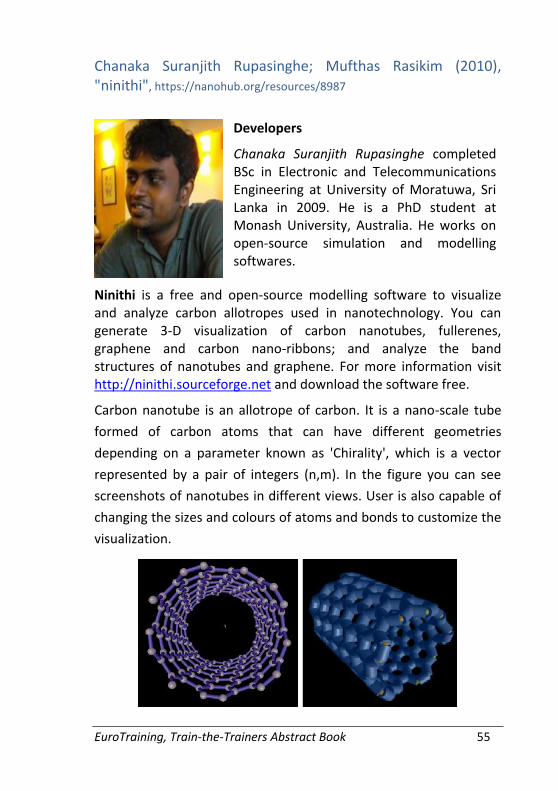
Carbon nanotube is an allotrope of carbon. It is a nano-scale tube
formed of carbon atoms that can have different geometries
depending on a parameter known as 'Chirality', which is a vector
represented by a pair of integers (n,m). In the figure you can see
screenshots of nanotubes in different views. User is also capable of
changing the sizes and colours of atoms and bonds to customize the
visualization.
56 EuroTraining, Train-the-Trainers Abstract Book
Chanaka Suranjith Rupasinghe; Mufthas Rasikim (2010),
"ninithi", https://nanohub.org/resources/8987
Developers
Mufthas Rasikim specialized in Electronic and Telecommunication Engineering from University of Moratuwa, Sri Lanka. Currently he is working for Lanka Software Foundation and together with scientists in Sri Lanka Institute of Nanotechnology to develop open-source software for nanotechnology.
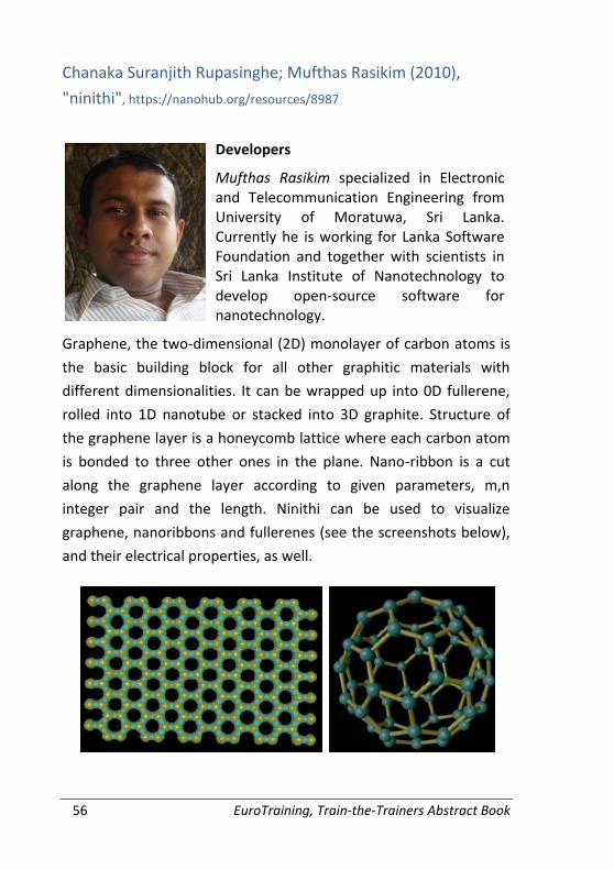
Graphene, the two-dimensional (2D) monolayer of carbon atoms is
the basic building block for all other graphitic materials with
different dimensionalities. It can be wrapped up into 0D fullerene,
rolled into 1D nanotube or stacked into 3D graphite. Structure of
the graphene layer is a honeycomb lattice where each carbon atom
is bonded to three other ones in the plane. Nano-ribbon is a cut
along the graphene layer according to given parameters, m,n
integer pair and the length. Ninithi can be used to visualize
graphene, nanoribbons and fullerenes (see the screenshots below),
and their electrical properties, as well.