Embed Size (px)
Citation preview

0.47uF
SDA
VDD
1.8V
LDO
Li-Ion
CellT
NFET
Protection
IC
PACKN
PACKP
Battery Pack
SCLI2C
Bus
BAT
SRN
VSSbq27441
NFET
VSYS
Coulomb
Counter
ADC
CPU
GPOUT
BIN
SRP
bq27441-G1
www.ti.com SLUSBH1A –NOVEMBER 2013–REVISED JANUARY 2014
System-Side Impedance Track™ Fuel GaugeCheck for Samples: bq27441-G1
1FEATURES APPLICATIONS23• Single Series Cell Li-Ion Battery Fuel Gauge • Smartphones, Feature Phones and Tablets
– Resides on System Board • Digital Still and Video Cameras– Supports Embedded or Removable • Handheld Terminals
Batteries • MP3 or Multimedia Players– Powered Directly from Battery with
Integrated LDO DESCRIPTIONThe Texas Instruments bq27441-G1 is an easy to– Supports a Low-Value External Senseconfigure microcontroller peripheral that providesResistor (10mΩ)system-side fuel gauging for single-cell Li-Ion• Easy to Configure Fuel Gauging Based on batteries. The device requires minimal userPatented Impedance Track™ Technology configuration and system microcontroller firmware
– Reports Remaining Capacity and State of development.Charge (SOC) with Smoothing Filter The bq27441-G1 uses the patented Impedance
– Automatically Adjusts for Battery Aging, Track™ algorithm for fuel gauging, and providesSelf-discharge, Temperature, and Rate information such as remaining battery capacityChanges (mAh), state-of-charge (%), and battery voltage (mV).
– Battery State of Health (Aging) Estimation Battery fuel gauging with the bq27441-G1 requires• Microcontroller Peripheral Supports: connections only to PACK+ (P+) and PACK– (P–) for
a removable battery pack or embedded battery– 400-kHz I2C™ Serial Interfacecircuit. The tiny 12-pin 2.5 mm × 4 mm SON package– Configurable SOC Interrupt, or is ideal for space constrained applications.
Battery Low Digital Output Warning– Internal Temperature Sensor, or
Host Reported Temperature• Small 12-pin 2.5 mm × 4 mm SON Package
TYPICAL APPLICATION
1
Please be aware that an important notice concerning availability, standard warranty, and use in critical applications ofTexas Instruments semiconductor products and disclaimers thereto appears at the end of this data sheet.
2Impedance Track is a trademark of Texas Instruments.3I2C is a trademark of NXP B.V. Corp Netherlands.PRODUCTION DATA information is current as of publication date. Copyright © 2013–2014, Texas Instruments IncorporatedProducts conform to specifications per the terms of the TexasInstruments standard warranty. Production processing does notnecessarily include testing of all parameters.

bq27441-G1
SLUSBH1A –NOVEMBER 2013–REVISED JANUARY 2014 www.ti.com
These devices have limited built-in ESD protection. The leads should be shorted together or the device placed in conductive foamduring storage or handling to prevent electrostatic damage to the MOS gates.
DEVICE INFORMATION
AVAILABLE OPTIONS
BATTERY FIRMWAREPART NUMBER CHEM_ID (1) DM_CODE (2) PACKAGE (4)TYPE VERSION (3)
bq27441DRZR-G1A LiCoO2 0x0128 0x48 12-pin,(4.2 V max charge)bq27441DRZT-G1A 1.09 2.5 × 4 mm(0x0109)bq27441DRZR-G1B LiMn2O4 SON0x0312 0x58(4.3 - 4.35 V max charge)bq27441DRZT-G1B
(1) See the CHEM_ID subcommand to confirm the battery chemistry type.(2) See the DM_CODE subcommand to confirm the Data Memory code.(3) See the FW_VERSION subcommand to confirm the firmware version.(4) For the most current package and ordering information see the Package Option Addendum at the end of this document; or, see the TI
website at www.ti.com.
THERMAL INFORMATIONbq27441-G1
THERMAL METRIC (1) UNITSDRZ (12-PINS)
θJA Junction-to-ambient thermal resistance 64.1θJCtop Junction-to-case (top) thermal resistance 59.8θJB Junction-to-board thermal resistance 52.7
°C/WψJT Junction-to-top characterization parameter 0.3ψJB Junction-to-board characterization parameter 28.3θJCbot Junction-to-case (bottom) thermal resistance 2.4
(1) For more information about traditional and new thermal metrics, see the IC Package Thermal Metrics application report, SPRA953.
2 Submit Documentation Feedback Copyright © 2013–2014, Texas Instruments Incorporated
Product Folder Links: bq27441-G1
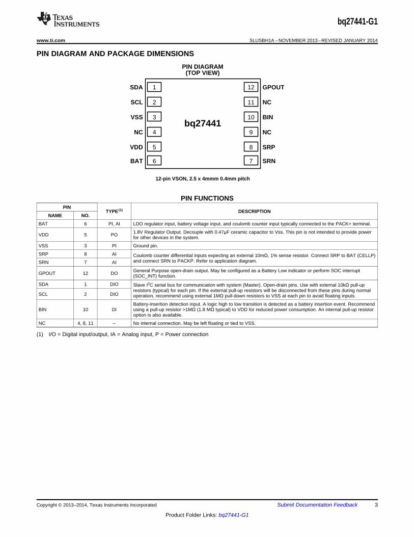
bq27441
1 12SDA GPOUT
VDD
2
3
4
5
11
10
9
8
NC
VSS
SCL
SRP
NC
BIN
NC
BAT 6 7 SRN
PIN DIAGRAM(TOP VIEW)
12-pin VSON, 2.5 x 4mmm 0.4mm pitch
bq27441-G1
www.ti.com SLUSBH1A –NOVEMBER 2013–REVISED JANUARY 2014
PIN DIAGRAM AND PACKAGE DIMENSIONS
PIN FUNCTIONSPIN
TYPE (1) DESCRIPTIONNAME NO.
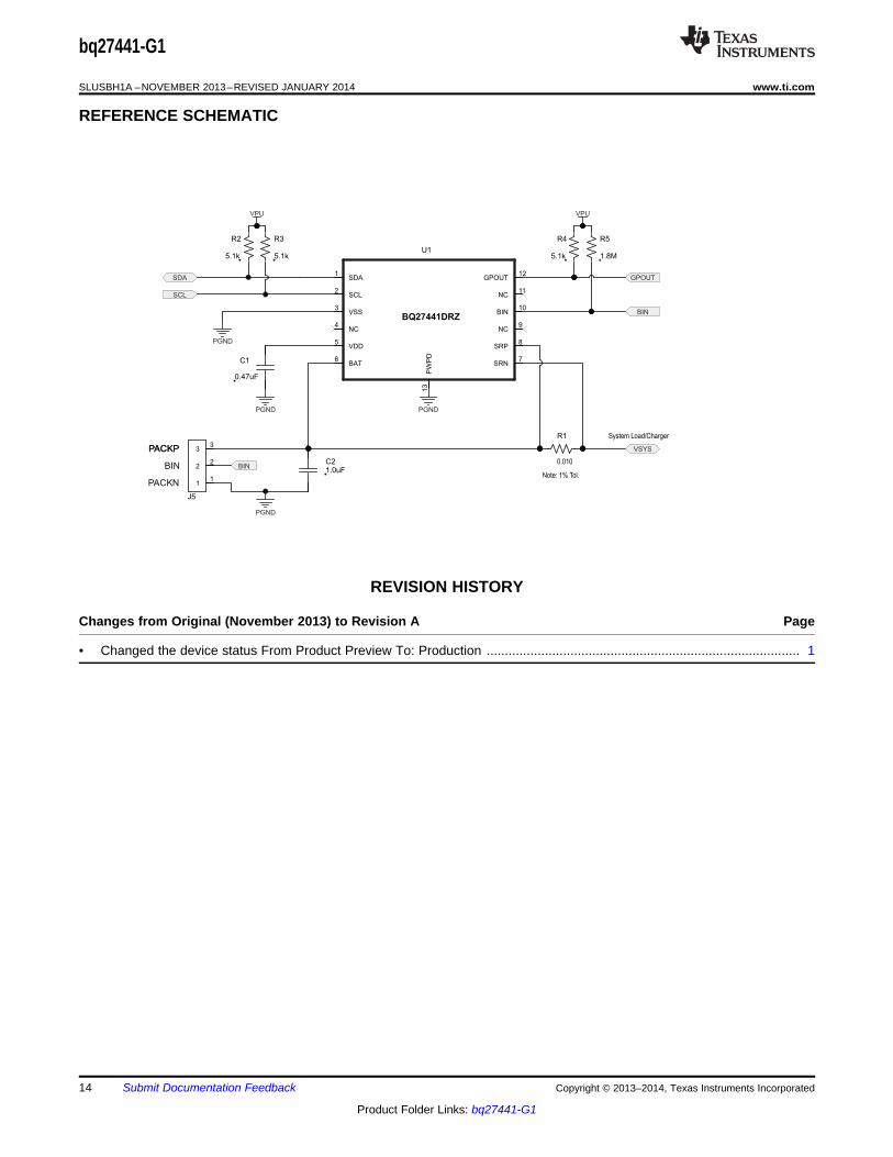
BAT 6 PI, AI LDO regulator input, battery voltage input, and coulomb counter input typically connected to the PACK+ terminal.
1.8V Regulator Output. Decouple with 0.47μF ceramic capacitor to Vss. This pin is not intended to provide powerVDD 5 PO for other devices in the system.
VSS 3 PI Ground pin.
SRP 8 AI Coulomb counter differential inputs expecting an external 10mΩ, 1% sense resistor. Connect SRP to BAT (CELLP)and connect SRN to PACKP. Refer to application diagram.SRN 7 AI
General Purpose open-drain output. May be configured as a Battery Low indicator or perform SOC interruptGPOUT 12 DO (SOC_INT) function.
SDA 1 DIO Slave I2C serial bus for communication with system (Master). Open-drain pins. Use with external 10kΩ pull-upresistors (typical) for each pin. If the external pull-up resistors will be disconnected from these pins during normal
SCL 2 DIO operation, recommend using external 1MΩ pull-down resistors to VSS at each pin to avoid floating inputs.
Battery-insertion detection input. A logic high to low transition is detected as a battery insertion event. RecommendBIN 10 DI using a pull-up resistor >1MΩ (1.8 MΩ typical) to VDD for reduced power consumption. An internal pull-up resistor
option is also available.
NC 4, 8, 11 -- No internal connection. May be left floating or tied to VSS.
(1) I/O = Digital input/output, IA = Analog input, P = Power connection
Copyright © 2013–2014, Texas Instruments Incorporated Submit Documentation Feedback 3
Product Folder Links: bq27441-G1

bq27441-G1
SLUSBH1A –NOVEMBER 2013–REVISED JANUARY 2014 www.ti.com
ELECTRICAL SPECIFICATIONS
ABSOLUTE MAXIMUM RATINGSover operating free-air temperature range (unless otherwise noted) (1)
PARAMETER MIN MAX UNITVBAT BAT pin input voltage range –0.3 6 V
SRP and SRN pins input voltage range -0.3 [VBAT + 0.3] VVSR Differential voltage across SRP and SRN. ABS(SRP - SRN). 2 VVDD VDD pin supply voltage range (LDO ouptut) –0.3 2 VVIOD Open-drain I/O pins (SDA, SCL) –0.3 6 VVIOPP Push-Pull I/O pins (BIN ) –0.3 [VDD + 0.3] VTA Operating free-air temperature range –40 85 °CTSTG Storage temperature range –65 150 °C
(1) Stresses beyond those listed under "absolute maximum ratings" may cause permanent damage to the device. These are stress ratingsonly, and functional operation of the device at these or any other conditions beyond those indicated under "recommended operatingconditions" is not implied. Exposure to absolute-maximum-rated conditions for extended periods may affect device reliability.
RECOMMENDED OPERATING CONDITIONSTA = 30°C and VREGIN = VBAT = 3.6V (unless otherwise noted)
PARAMETER TEST CONDITIONS MIN TYP MAX UNIT
External input capacitor for internalCBAT(1) 0.1 μFNominal capacitor values specified.LDO between BAT and VSS
Recommend a 5% ceramic X5R typeExternal output capacitor for internal capacitor located close to the device.CLDO18
(1) 0.47 μFLDO between VDD and VSS
External pull-up voltage for open-VPU(1) 1.62 3.6 Vdrain pins (SDA, SCL, GPOUT )
(1) Specified by design. Not production tested.
SUPPLY CURRENTTA = 30°C and VREGIN = VBAT = 3.6V (unless otherwise noted)
PARAMETER TEST CONDITIONS MIN TYP MAX UNITICC
(1) NORMAL mode current ILOAD > Sleep Current (2) 93 μAISLP
(1) SLEEP mode current ILOAD < Sleep Current (2) 21 μAIHIB
(1) HIBERNATE mode current ILOAD < Hibernate Current (2) 9 μAFuel gauge in host commanded
ISD(1) SHUTDOWN mode current SHUTDOWN mode. 0.6 μA
(LDO Regulator Output Disabled.)
(1) Specified by design. Not production tested.(2) Wake Comparator Disabled.
4 Submit Documentation Feedback Copyright © 2013–2014, Texas Instruments Incorporated
Product Folder Links: bq27441-G1

bq27441-G1
www.ti.com SLUSBH1A –NOVEMBER 2013–REVISED JANUARY 2014
DIGITAL INPUT AND OUTPUT DC CHARACTERISTICSTA = –40°C to 85°C, typical values at TA = 30°C and VREGIN = 3.6 V (unless otherwise noted)(Force Note1) (1)
PARAMETER TEST CONDITIONS MIN TYP MAX UNITVIH(OD) Input voltage, high (2) External pullup resistor to VPU VPU x 0.7 VVIH(PP) Input voltage, high (3) 1.4 VVIL Input voltage, low (2) (3) 0.6 VVOL Output voltage, low (2) 0.6 VIOH Output source current, high (2) 0.5 mAIOL(OD) Output sink current, low (2) -3 mACIN
(1) Input capacitance (2) (3) 5 pFInput leakage current (I/O pins)Ilkg 1 μA(2) (3)
(1) Specified by design. Not production tested.(2) Open Drain pins: (SCL, SDA, GPOUT )(3) Push Pull pin: (BIN )
LDO REGULATOR, WAKE-UP AND AUTO-SHUTDOWN DC CHARACTERISTICSTA = –40°C to 85°C, typical values at TA = 30°C and VREGIN = 3.6 V (unless otherwise noted)(Force Note1) (1)
PARAMETER TEST CONDITIONS MIN TYP MAX UNITVBAT BAT pin regulator input 2.45 4.5 VVDD Regulator output voltage 1.8 V
VBAT Under Voltage Lock OutUVLOIT+ 2 VLDO Wake-Up Rising ThresholdVBAT Under Voltage Lock Out
UVLOIT- LDO Auto-Shutdown Falling 1.95 VThresholdGPOUT (input) LDO Wake-Up LDO Wake-up from SHUTDOWNVWU+
(1) 1.2 Vrising edge threshold (2) mode
(1) Specified by design. Not production tested.(2) If the device is commanded to SHUTDOWN via I2C with VBAT > UVLOIT+ , a wake-up rising edge trigger is required on GPOUT .
Copyright © 2013–2014, Texas Instruments Incorporated Submit Documentation Feedback 5
Product Folder Links: bq27441-G1

Active
REGIN
GPOUT *
VDD
State SHUTDOWN WAKE-UP
tSHUP
tSHDN tWUVDD
WAKE-UPOff Active
* GPOUT is configured as an input for wake-up signaling.
SHUTDOWNSHUTDOWN_ENABLE
I2C Bus
tPUCD tPUCD
tVDD
bq27441-G1
SLUSBH1A –NOVEMBER 2013–REVISED JANUARY 2014 www.ti.com
LDO REGULATOR, WAKE-UP AND AUTO-SHUTDOWN AC CHARACTERISTICSTA = –40°C to 85°C, typical values at TA = 30°C and VREGIN = 3.6 V (unless otherwise noted)(Force Note1) (1)
PARAMETER TEST CONDITIONS MIN TYP MAX UNITTime delay from SHUTDOWNtSHDN
(1) SHUTDOWN Entry Time 250 mscommand to LDO output disable.Minimum low time of GPOUT (input)tSHUP
(1) SHUTDOWN GPOUT Low time 10 μsin SHUTDOWN before WAKEUPtVDD
(1) Initial VDD Output delay 13 msTime delay from rising edge of
tWUVDD(1) Wake-up VDD Output delay GPOUT (input) to nominal VDD 8 ms
output.Time delay from rising edge of
tPUCD Power-up communication delay REGIN to the Active state. Includes 250 msfirmware initialization time.
(1) Specified by design. Not production tested.
SHUTDOWN and WAKE-UP Timing
Figure 1. SHUTDOWN and WAKE-UP Timing Diagram
6 Submit Documentation Feedback Copyright © 2013–2014, Texas Instruments Incorporated
Product Folder Links: bq27441-G1

bq27441-G1
www.ti.com SLUSBH1A –NOVEMBER 2013–REVISED JANUARY 2014
ADC (TEMPERATURE AND CELL MEASUREMENT) CHARACTERISTICSTA = –40°C to 85°C; typical values at TA = 30°C and VREGIN = 3.6 V (unless otherwise noted) (Force Note1) (1)
PARAMETER TEST CONDITIONS MIN TYP MAX UNITVIN(BAT) BAT pin voltage measurement Voltage divider enabled. 2.45 4.5 V
range.tADC_CONV Conversion time 125 ms
Effective Resolution 15 bits
(1) Specified by design. Not tested in production.
INTEGRATING ADC (COULOMB COUNTER) CHARACTERISTICSTA = –40°C to 85°C; typical values at TA = 30°C and VREGIN = 3.6 V (unless otherwise noted)(Force Note1) (1)
PARAMETER TEST CONDITIONS MIN TYP MAX UNITVSR Input voltage range from BAT to BAT ± 25 mV
SRX pinstSR_CONV Conversion time Single conversion 1 s
Effective Resolution Single conversion 16 bits
(1) Assured by design. Not tested in production.
Copyright © 2013–2014, Texas Instruments Incorporated Submit Documentation Feedback 7
Product Folder Links: bq27441-G1

tSU(STA)
SCL
SDA
tw(H) tw(L)tf tr t(BUF)
tr
td(STA)
REPEATEDSTART
th(DAT) tsu(DAT)
tf tsu(STOP)
STOP START
bq27441-G1
SLUSBH1A –NOVEMBER 2013–REVISED JANUARY 2014 www.ti.com
I2C-COMPATIBLE INTERFACE COMMUNICATION TIMING CHARACTERISTICSTA = –40°C to 85°C; typical values at TA = 30°C and VREGIN = 3.6 V (unless otherwise noted) (Force Note1) (1)
PARAMETER TEST CONDITIONS MIN TYP MAX UNITStandard Mode (100 kHz)td(STA) Start to first falling edge of SCL 4 μstw(L) SCL pulse duration (low) 4.7 μstw(H) SCL pulse duration (high) 4 μstsu(STA) Setup for repeated start 4.7 μstsu(DAT) Data setup time Host drives SDA 250 nsth(DAT) Data hold time Host drives SDA 0 nstsu(STOP) Setup time for stop 4 μst(BUF) Bus free time between stop and Includes Command Waiting Time 66 μs
starttf SCL/SDA fall time (1) 300 nstr SCL/SDA rise time (1) 300 nsfSCL Clock frequency (2) 100 kHzFast Mode (400 kHz)td(STA) Start to first falling edge of SCL 600 nstw(L) SCL pulse duration (low) 1300 nstw(H) SCL pulse duration (high) 600 nstsu(STA) Setup for repeated start 600 nstsu(DAT) Data setup time Host drives SDA 100 nsth(DAT) Data hold time Host drives SDA 0 nstsu(STOP) Setup time for stop 600 nst(BUF) Bus free time between stop and Includes Command Waiting Time 66 μs
starttf SCL/SDA fall time (1) 300 nstr SCL/SDA rise time (1) 300 nsfSCL Clock frequency (2) 400 kHz
(1) Specified by design. Not production tested.(2) If the clock frequency (fSCL) is > 100 kHz, use 1-byte write commands for proper operation. All other transactions types are supported at
400 kHz. (Refer to I2C INTERFACE and I2C Command Waiting Time)
Figure 2. I2C-Compatible Interface Timing Diagrams
8 Submit Documentation Feedback Copyright © 2013–2014, Texas Instruments Incorporated
Product Folder Links: bq27441-G1

bq27441-G1
www.ti.com SLUSBH1A –NOVEMBER 2013–REVISED JANUARY 2014
GENERAL DESCRIPTION
The bq27441-G1 accurately predicts the battery capacity and other operational characteristics of a single Li-based rechargeable cell. It can be interrogated by a system processor to provide cell information, such as state-of-charge (SOC).
Information is accessed through a series of commands, called Standard Commands. Further capabilities areprovided by the additional Extended Commands set. Both sets of commands, indicated by the general formatCommand( ), are used to read and write information contained within the bq27441-G1 control and statusregisters, as well as its data locations. Commands are sent from system to gauge using the bq27441-G1’s I2Cserial communications engine, and can be executed during application development, system manufacture, orend-equipment operation.
The key to the bq27441-G1’s high-accuracy gas gauging prediction is Texas Instrument’s proprietary ImpedanceTrack™ algorithm. This algorithm uses cell measurements, characteristics, and properties to create state-of-charge predictions that can achieve high accuracy across a wide variety of operating conditions and over thelifetime of the battery.
The bq27441-G1 measures charge/discharge activity by monitoring the voltage across a small-value senseresistor. When a cell is attached to the bq27441-G1, cell impedance is computed, based on cell current, cellopen-circuit voltage (OCV), and cell voltage under loading conditions.
The bq27441-G1 uses an integrated temperature sensor for estimating cell temperature. Alternatively, the hostprocessor can provide temperature data for the bq27441-G1.
To minimize power consumption, the bq27441-G1 has several power modes: INITIALIZATION, NORMAL,SLEEP, and HIBERNATE. The bq27441-G1 passes automatically between these modes, depending upon theoccurrence of specific events, though a system processor can initiate some of these modes directly. More detailsare found in the bq27441-G1 Technical Reference Manual (SLUUAC9).
NOTE
Formatting Conventions in this Document:
Commands: italics with parentheses( ) and no breaking spaces, for example,RemainingCapacity( ).
Data Flash: italics, bold, and breaking spaces, for example, Design Capacity.
Register bits and flags: italics with brackets [ ], for example, [TDA]
Data flash bits: italics, bold, and brackets [ ], for example, [LED1]Modes and states: ALL CAPITALS, for example, UNSEALED mode.
Copyright © 2013–2014, Texas Instruments Incorporated Submit Documentation Feedback 9
Product Folder Links: bq27441-G1

bq27441-G1
SLUSBH1A –NOVEMBER 2013–REVISED JANUARY 2014 www.ti.com
DATA COMMANDS
STANDARD DATA COMMANDSThe bq27441-G1 uses a series of 2-byte standard commands to enable system reading and writing of batteryinformation. Each standard command has an associated command-code pair, as indicated in . Because eachcommand consists of two bytes of data, two consecutive I2C transmissions must be executed both to initiate thecommand function, and to read or write the corresponding two bytes of data. Additional details are found in thebq27441-G1 Technical Reference Manual (SLUUAC9).
Table 1. Standard CommandsNAME COMMAND UNITS SEALED ACCESS
CODEControl( ) CNTL 0x00 / 0x01 N/A R/WTemperature( ) TEMP 0x02 / 0x03 0.1°K R/WVoltage( ) VOLT 0x04 / 0x05 mV RFlags( ) FLAGS 0x06 / 0x07 N/A RNominalAvailableCapacity( ) 0x08 / 0x09 mAh RFullAvailableCapacity( ) 0x0a / 0x0b mAh RRemainingCapacity( ) RM 0x0c / 0x0d mAh RFullChargeCapacity( ) FCC 0x0e / 0x0f mAh RAverageCurrent( ) 0x10 / 0x11 mA RStandbyCurrent( ) 0x12 / 0x13 mA RMaxLoadCurrent( ) 0x14 / 0x15 mA RAveragePower( ) 0x18 / 0x19 mW RStateOfCharge( ) SOC 0x1c / 0x1d % RIntTemperature( ) 0x1e / 0x1f 0.1°K RStateOfHealth( ) SOH 0x20 / 0x21 num / % R
10 Submit Documentation Feedback Copyright © 2013–2014, Texas Instruments Incorporated
Product Folder Links: bq27441-G1

bq27441-G1
www.ti.com SLUSBH1A –NOVEMBER 2013–REVISED JANUARY 2014
Control( ): 0x00/0x01Issuing a Control( ) command requires a subsequent 2-byte subcommand. These additional bytes specify theparticular control function desired. The Control( ) command allows the system to control specific features of thebq27441-G1 during normal operation and additional features when the device is in different access modes, asdescribed in . Additional details are found in the bq27441-G1 Technical Reference Manual (SLUUAC9).
Table 2. Control( ) SubcommandsCNTL FUNCTION CNTL DATA SEALED ACCESS DESCRIPTIONCONTROL_STATUS 0x0000 Yes Reports the status of device.DEVICE_TYPE 0x0001 Yes Reports the device type (0x0421).FW_VERSION 0x0002 Yes Reports the firmware version of the device.DM_CODE 0x0004 Yes Reports the Data Memory Code number stored in NVM.PREV_MACWRITE 0x0007 Yes Returns previous MAC command code.CHEM_ID 0x0008 Yes Reports the chemical identifier of the Impedance Track™ configurationBAT_INSERT 0x000c Yes Forces the [BAT_DET] bit set when the [BIE] bit is 0.BAT_REMOVE 0x000d Yes Forces the [BAT_DET] bit clear when the [BIE] bit is 0.SET_HIBERNATE 0x0011 Yes Forces CONTROL_STATUS [HIBERNATE] to 1.CLEAR_HIBERNATE 0x0012 Yes Forces CONTROL_STATUS [HIBERNATE] to 0.SET_CFGUPDATE 0x0013 No Force CONTROL_STATUS [CFGUPMODE] to 1 and gauge enters
CONFIG UPDATE mode.SHUTDOWN_ENABLE 0x001b No Enables device SHUTDOWN mode.SHUTDOWN 0x001c No Commands the device to enter SHUTDOWN mode.SEALED 0x0020 No Places the device in SEALED access mode.TOGGLE_GPOUT 0x0023 Yes Commands the device to toggle the GPOUT pin for 1ms.RESET 0x0041 No Performs a full device reset.SOFT_RESET 0x0042 No Gauge exits CONFIG UPDATE mode.
See the bq27441-G1 Technical Reference Manual for detailed descriptions for the Standard Data Commandsand Control( ) subcommands.
Copyright © 2013–2014, Texas Instruments Incorporated Submit Documentation Feedback 11
Product Folder Links: bq27441-G1

Host generated
A AS 0ADDR[6:0] CMD[7:0] Sr 1ADDR[6:0] A DATA [7:0] A DATA [7:0] PN. . .
(d) incremental read
A AS 0ADDR[6:0] CMD[7:0] Sr 1ADDR[6:0] A DATA [7:0] PN
(c) 1- byte read
A AS A0 PADDR[6:0] CMD[7:0] DATA [7:0]
(a) 1-byte write (b) quick read
S 1ADDR[6:0] A DATA [7:0] PN
Gauge generated
. . .A AS A0 PADDR[6:0] CMD[7:0] DATA [7:0] DATA [7:0] A A
(e) incremental write
(S = Start , Sr = Repeated Start , A = Acknowledge , N = No Acknowledge , and P = Stop).
bq27441-G1
SLUSBH1A –NOVEMBER 2013–REVISED JANUARY 2014 www.ti.com
FUNCTIONAL DESCRIPTION
I2C INTERFACEThe bq27441-G1 supports the standard I2C read, incremental read, quick read, one-byte write, and incrementalwrite functions. The 7-bit device address (ADDR) is the most significant 7 bits of the hex address and is fixed as1010101. The first 8 bits of the I2C protocol are, therefore, 0xAA or 0xAB for write or read, respectively.
The quick read returns data at the address indicated by the address pointer. The address pointer, a registerinternal to the I2C communication engine, increments whenever data is acknowledged by the bq27441-G1 or theI2C master. “Quick writes” function in the same manner and are a convenient means of sending multiple bytes toconsecutive command locations (such as two-byte commands that require two bytes of data).
The following command sequences are not supported:Attempt to write a read-only address (NACK after data sent by master):
Attempt to read an address above 0x6B (NACK command):
I2C Time OutThe I2C engine releases both SDA and SCL if the I2C bus is held low for 2 seconds. If the bq27441-G1 is holdingthe lines, releasing them frees them for the master to drive the lines. If an external condition is holding either ofthe lines low, the I2C engine enters the low-power sleep mode.
12 Submit Documentation Feedback Copyright © 2013–2014, Texas Instruments Incorporated
Product Folder Links: bq27441-G1

A AS 0ADDR [6:0] CMD [7:0] Sr 1ADDR [6:0] A DATA [7:0] A DATA [7:0] PN
A AS A0 PADDR [6:0] CMD [7:0] DATA [7:0] DATA [7:0] A 66 sm
A AS 0ADDR [6:0] CMD [7:0] Sr 1ADDR [6:0] A DATA [7:0] A DATA [7:0] A
DATA [7:0] A DATA [7:0] PN
Waiting time inserted between incremental 2-byte write packet for a subcommand and reading results
(acceptable for 100 kHz)fSCL £
Waiting time inserted after incremental read
66 sm
66 sm
A AS 0ADDR [6:0] CMD [7:0] Sr 1ADDR [6:0] A DATA [7:0] A DATA [7:0] PN
A AS A0 PADDR [6:0] CMD [7:0] DATA [7:0] 66 sm
Waiting time inserted between two 1-byte write packets for a subcommand and reading results
(required for 100 kHz < f 400 kHz)SCL £
66 sm
A AS A0 PADDR [6:0] CMD [7:0] DATA [7:0] 66 sm
bq27441-G1
www.ti.com SLUSBH1A –NOVEMBER 2013–REVISED JANUARY 2014
I2C Command Waiting TimeTo ensure proper operation at 400 kHz, a t(BUF) ≥ 66 μs bus-free waiting time must be inserted between allpackets addressed to the bq27441-G1. In addition, if the SCL clock frequency (fSCL) is > 100 kHz, use individual1-byte write commands for proper data flow control. The following diagram shows the standard waiting timerequired between issuing the control subcommand the reading the status result. For read-write standardcommand, a minimum of 2 seconds is required to get the result updated. For read-only standard commands,there is no waiting time required, but the host must not issue any standard command more than two times persecond. Otherwise, the gauge could result in a reset issue due to the expiration of the watchdog timer.
I2C Clock StretchingA clock stretch can occur during all modes of fuel gauge operation. In SLEEP and HIBERNATE modes, a short ≤100 µs clock stretch occurs on all I2C traffic as the device must wake-up to process the packet. In the othermodes ( INITIALIZATION , NORMAL) a ≤ 4 ms clock stretching period may occur within packets addressed forthe fuel gauge as the I2C interface performs normal data flow control.
Copyright © 2013–2014, Texas Instruments Incorporated Submit Documentation Feedback 13
Product Folder Links: bq27441-G1
PACKP
SDA1
SCL2
VSS3
NC4
VDD5
BAT6
SRN7
SRP8
NC9
BIN10
NC11
GPOUT12
PW
PD
13
U1
BQ27441DRZ
PGND
0.47uF
C1
PGND
PGND
0.010
R1
Note: 1% Tol.1.0uF
C2
PGND
11
22
33
J5
BIN
SCL
SDA
BIN
PACKP
PACKN
VSYS
VPU
5.1k
R2
5.1k
R3
VPU
5.1k
R4
1.8M
R5
GPOUT
BIN
System Load/Charger
bq27441-G1
SLUSBH1A –NOVEMBER 2013–REVISED JANUARY 2014 www.ti.com
REFERENCE SCHEMATIC
spacer
REVISION HISTORY
Changes from Original (November 2013) to Revision A Page
• Changed the device status From Product Preview To: Production ...................................................................................... 1
14 Submit Documentation Feedback Copyright © 2013–2014, Texas Instruments Incorporated
Product Folder Links: bq27441-G1

PACKAGE OPTION ADDENDUM
www.ti.com 20-Jan-2014
Addendum-Page 1
PACKAGING INFORMATION
Orderable Device Status(1)
Package Type PackageDrawing
Pins PackageQty
Eco Plan(2)
Lead/Ball Finish(6)
MSL Peak Temp(3)
Op Temp (°C) Device Marking(4/5)
Samples
BQ27441DRZR-G1A ACTIVE SON DRZ 12 3000 Green (RoHS& no Sb/Br)
CU NIPDAU Level-2-260C-1 YEAR -40 to 85 BQ27441A
BQ27441DRZR-G1B ACTIVE SON DRZ 12 3000 Green (RoHS& no Sb/Br)
CU NIPDAU Level-2-260C-1 YEAR -40 to 85 BQ27441B
BQ27441DRZT-G1A ACTIVE SON DRZ 12 250 Green (RoHS& no Sb/Br)
CU NIPDAU Level-2-260C-1 YEAR -40 to 85 BQ27441A
BQ27441DRZT-G1B ACTIVE SON DRZ 12 250 Green (RoHS& no Sb/Br)
CU NIPDAU Level-2-260C-1 YEAR -40 to 85 BQ27441B
(1) The marketing status values are defined as follows:ACTIVE: Product device recommended for new designs.LIFEBUY: TI has announced that the device will be discontinued, and a lifetime-buy period is in effect.NRND: Not recommended for new designs. Device is in production to support existing customers, but TI does not recommend using this part in a new design.PREVIEW: Device has been announced but is not in production. Samples may or may not be available.OBSOLETE: TI has discontinued the production of the device.
(2) Eco Plan - The planned eco-friendly classification: Pb-Free (RoHS), Pb-Free (RoHS Exempt), or Green (RoHS & no Sb/Br) - please check http://www.ti.com/productcontent for the latest availabilityinformation and additional product content details.TBD: The Pb-Free/Green conversion plan has not been defined.Pb-Free (RoHS): TI's terms "Lead-Free" or "Pb-Free" mean semiconductor products that are compatible with the current RoHS requirements for all 6 substances, including the requirement thatlead not exceed 0.1% by weight in homogeneous materials. Where designed to be soldered at high temperatures, TI Pb-Free products are suitable for use in specified lead-free processes.Pb-Free (RoHS Exempt): This component has a RoHS exemption for either 1) lead-based flip-chip solder bumps used between the die and package, or 2) lead-based die adhesive used betweenthe die and leadframe. The component is otherwise considered Pb-Free (RoHS compatible) as defined above.Green (RoHS & no Sb/Br): TI defines "Green" to mean Pb-Free (RoHS compatible), and free of Bromine (Br) and Antimony (Sb) based flame retardants (Br or Sb do not exceed 0.1% by weightin homogeneous material)
(3) MSL, Peak Temp. - The Moisture Sensitivity Level rating according to the JEDEC industry standard classifications, and peak solder temperature.
(4) There may be additional marking, which relates to the logo, the lot trace code information, or the environmental category on the device.
(5) Multiple Device Markings will be inside parentheses. Only one Device Marking contained in parentheses and separated by a "~" will appear on a device. If a line is indented then it is a continuationof the previous line and the two combined represent the entire Device Marking for that device.
(6) Lead/Ball Finish - Orderable Devices may have multiple material finish options. Finish options are separated by a vertical ruled line. Lead/Ball Finish values may wrap to two lines if the finishvalue exceeds the maximum column width.

PACKAGE OPTION ADDENDUM
www.ti.com 20-Jan-2014
Addendum-Page 2
Important Information and Disclaimer:The information provided on this page represents TI's knowledge and belief as of the date that it is provided. TI bases its knowledge and belief on informationprovided by third parties, and makes no representation or warranty as to the accuracy of such information. Efforts are underway to better integrate information from third parties. TI has taken andcontinues to take reasonable steps to provide representative and accurate information but may not have conducted destructive testing or chemical analysis on incoming materials and chemicals.TI and TI suppliers consider certain information to be proprietary, and thus CAS numbers and other limited information may not be available for release.
In no event shall TI's liability arising out of such information exceed the total purchase price of the TI part(s) at issue in this document sold by TI to Customer on an annual basis.

TAPE AND REEL INFORMATION
*All dimensions are nominal
Device PackageType
PackageDrawing
Pins SPQ ReelDiameter
(mm)
ReelWidth
W1 (mm)
A0(mm)
B0(mm)
K0(mm)
P1(mm)
W(mm)
Pin1Quadrant
BQ27441DRZR-G1A SON DRZ 12 3000 330.0 12.4 2.8 4.3 1.2 4.0 12.0 Q2
BQ27441DRZR-G1B SON DRZ 12 3000 330.0 12.4 2.8 4.3 1.2 4.0 12.0 Q2
BQ27441DRZT-G1A SON DRZ 12 250 180.0 12.4 2.8 4.3 1.2 4.0 12.0 Q2
BQ27441DRZT-G1B SON DRZ 12 250 180.0 12.4 2.8 4.3 1.2 4.0 12.0 Q2
PACKAGE MATERIALS INFORMATION
www.ti.com 30-Jan-2014
Pack Materials-Page 1

*All dimensions are nominal
Device Package Type Package Drawing Pins SPQ Length (mm) Width (mm) Height (mm)
BQ27441DRZR-G1A SON DRZ 12 3000 367.0 367.0 35.0
BQ27441DRZR-G1B SON DRZ 12 3000 367.0 367.0 35.0
BQ27441DRZT-G1A SON DRZ 12 250 210.0 185.0 35.0
BQ27441DRZT-G1B SON DRZ 12 250 210.0 185.0 35.0
PACKAGE MATERIALS INFORMATION
www.ti.com 30-Jan-2014
Pack Materials-Page 2


IMPORTANT NOTICETexas Instruments Incorporated and its subsidiaries (TI) reserve the right to make corrections, enhancements, improvements and otherchanges to its semiconductor products and services per JESD46, latest issue, and to discontinue any product or service per JESD48, latestissue. Buyers should obtain the latest relevant information before placing orders and should verify that such information is current andcomplete. All semiconductor products (also referred to herein as “components”) are sold subject to TI’s terms and conditions of salesupplied at the time of order acknowledgment.TI warrants performance of its components to the specifications applicable at the time of sale, in accordance with the warranty in TI’s termsand conditions of sale of semiconductor products. Testing and other quality control techniques are used to the extent TI deems necessaryto support this warranty. Except where mandated by applicable law, testing of all parameters of each component is not necessarilyperformed.TI assumes no liability for applications assistance or the design of Buyers’ products. Buyers are responsible for their products andapplications using TI components. To minimize the risks associated with Buyers’ products and applications, Buyers should provideadequate design and operating safeguards.TI does not warrant or represent that any license, either express or implied, is granted under any patent right, copyright, mask work right, orother intellectual property right relating to any combination, machine, or process in which TI components or services are used. Informationpublished by TI regarding third-party products or services does not constitute a license to use such products or services or a warranty orendorsement thereof. Use of such information may require a license from a third party under the patents or other intellectual property of thethird party, or a license from TI under the patents or other intellectual property of TI.Reproduction of significant portions of TI information in TI data books or data sheets is permissible only if reproduction is without alterationand is accompanied by all associated warranties, conditions, limitations, and notices. TI is not responsible or liable for such altereddocumentation. Information of third parties may be subject to additional restrictions.Resale of TI components or services with statements different from or beyond the parameters stated by TI for that component or servicevoids all express and any implied warranties for the associated TI component or service and is an unfair and deceptive business practice.TI is not responsible or liable for any such statements.Buyer acknowledges and agrees that it is solely responsible for compliance with all legal, regulatory and safety-related requirementsconcerning its products, and any use of TI components in its applications, notwithstanding any applications-related information or supportthat may be provided by TI. Buyer represents and agrees that it has all the necessary expertise to create and implement safeguards whichanticipate dangerous consequences of failures, monitor failures and their consequences, lessen the likelihood of failures that might causeharm and take appropriate remedial actions. Buyer will fully indemnify TI and its representatives against any damages arising out of the useof any TI components in safety-critical applications.In some cases, TI components may be promoted specifically to facilitate safety-related applications. With such components, TI’s goal is tohelp enable customers to design and create their own end-product solutions that meet applicable functional safety standards andrequirements. Nonetheless, such components are subject to these terms.No TI components are authorized for use in FDA Class III (or similar life-critical medical equipment) unless authorized officers of the partieshave executed a special agreement specifically governing such use.Only those TI components which TI has specifically designated as military grade or “enhanced plastic” are designed and intended for use inmilitary/aerospace applications or environments. Buyer acknowledges and agrees that any military or aerospace use of TI componentswhich have not been so designated is solely at the Buyer's risk, and that Buyer is solely responsible for compliance with all legal andregulatory requirements in connection with such use.TI has specifically designated certain components as meeting ISO/TS16949 requirements, mainly for automotive use. In any case of use ofnon-designated products, TI will not be responsible for any failure to meet ISO/TS16949.Products ApplicationsAudio www.ti.com/audio Automotive and Transportation www.ti.com/automotiveAmplifiers amplifier.ti.com Communications and Telecom www.ti.com/communicationsData Converters dataconverter.ti.com Computers and Peripherals www.ti.com/computersDLP® Products www.dlp.com Consumer Electronics www.ti.com/consumer-appsDSP dsp.ti.com Energy and Lighting www.ti.com/energyClocks and Timers www.ti.com/clocks Industrial www.ti.com/industrialInterface interface.ti.com Medical www.ti.com/medicalLogic logic.ti.com Security www.ti.com/securityPower Mgmt power.ti.com Space, Avionics and Defense www.ti.com/space-avionics-defenseMicrocontrollers microcontroller.ti.com Video and Imaging www.ti.com/videoRFID www.ti-rfid.comOMAP Applications Processors www.ti.com/omap TI E2E Community e2e.ti.comWireless Connectivity www.ti.com/wirelessconnectivity
Mailing Address: Texas Instruments, Post Office Box 655303, Dallas, Texas 75265Copyright © 2014, Texas Instruments Incorporated