Embed Size (px)
Citation preview

Prof. Rao R. Tummala Joseph M. Pettit Endowed Chair
Professor in ECE & MSEDirector, 3D Microsystems Packaging Research Center
Georgia Institute of Technology – Atlanta, GA [email protected]
System Scalingfor
New Era of Automotive Electronics: A Large-scale Industry Consortium at Georgia Tech
in Partnership withGlobal Supply-Chain Mfg and OEMs
SRC June 7, 2016

1 | SRC Prof. Rao R. Tummala
Outline
System Scaling as a Microelectronics Technology Frontier
New Era of Automotive Electronics (NAE) Industry Consortium at GT
• Faculty• Industry Partners• Facilities• Technical Programs
Computing and Communication Electronics Sensing Electronics High Power and High Temperature Electronics
Summary

2 | SRC Prof. Rao R. Tummala
SYSTEM SCALING AS A MICROELECTRONICSSYSTEMS TECHNOLOGY FRONTIER

3 | SRC Prof. Rao R. Tummala
Georgia Tech PRC Center started with a Vision For Digital Convergence by SOP Concept in 1993
Digital + Analog + RF + Optical + Sensors Computing/Internet Digital Audio Digital Imaging/Video Cellular/Wireless GPS/Satellite Sensors And, of course, timekeeping!
4 | SRC Prof. Rao R. Tummala
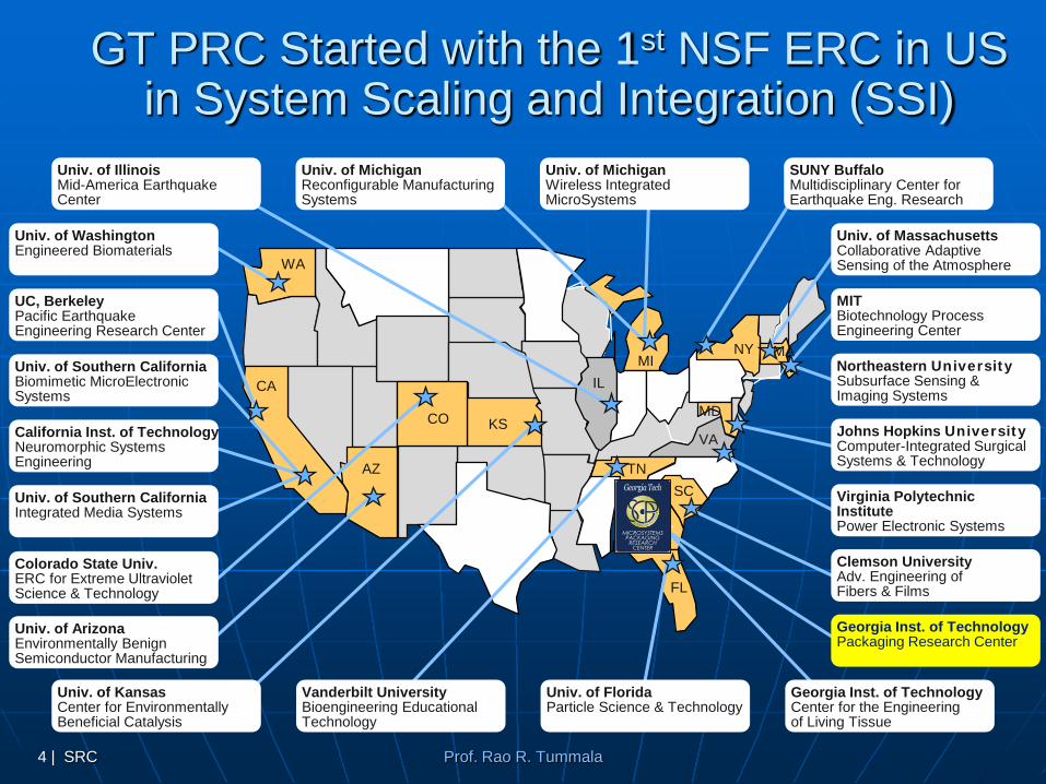
GT PRC Started with the 1st NSF ERC in US in System Scaling and Integration (SSI)
WA
CA
AZ
CO KS
TN
GASC
FL
VA
MINY
MD
MA
IL
Georgia Inst. of TechnologyPackaging Research Center
Clemson UniversityAdv. Engineering ofFibers & Films
Georgia Inst. of TechnologyCenter for the Engineeringof Living Tissue
Virginia Polytechnic InstitutePower Electronic Systems
MITBiotechnology Process Engineering Center
Johns Hopkins UniversityComputer-Integrated Surgical Systems & Technology
Vanderbilt UniversityBioengineering Educational Technology
Univ. of FloridaParticle Science & Technology
Northeastern UniversitySubsurface Sensing & Imaging Systems
Colorado State Univ.ERC for Extreme UltravioletScience & Technology
Univ. of KansasCenter for Environmentally Beneficial Catalysis
Univ. of MassachusettsCollaborative Adaptive Sensing of the Atmosphere
Univ. of MichiganReconfigurable Manufacturing Systems
Univ. of MichiganWireless Integrated MicroSystems
SUNY BuffaloMultidisciplinary Center for Earthquake Eng. Research
Univ. of IllinoisMid-America Earthquake Center
California Inst. of TechnologyNeuromorphic Systems Engineering
Univ. of Southern CaliforniaIntegrated Media Systems
Univ. of Southern CaliforniaBiomimetic MicroElectronicSystems
UC, BerkeleyPacific EarthquakeEngineering Research Center
Univ. of WashingtonEngineered Biomaterials
Univ. of ArizonaEnvironmentally Benign Semiconductor Manufacturing

5 | SRC Prof. Rao R. Tummala
SOP @ PRC“Package is the System”
System: Convergent Computing, Communication, Consumer & Biomedical
SOP

6 | SRC Prof. Rao R. Tummala
IC-Package Trend
SOC 2D MCM 3D ICs SIP
SOP

7 | SRC Prof. Rao R. Tummala
Outcomes of Georgia Tech’s NSF ERC & Model
Research & Infrastructure
System Scaling for Smart phones 2000 ground-breaking publications 20 Faculty and 150 grad students 100 Best Paper Awards $40M SOA Laboratories
Education
Interdisciplinary Engineers Ph.D ~500,MS ~570,BS ~340
Created 20 new courses 1st undergrad & 1st Grad. book
Global IndustryCollaborations
150 US, 25 Jap., 10 Eu, 10 Korean 10 Spin-off and spin-in companies 70 Patents, and 166 IP licenses 97 Technology transfers
Funds RaisedEconomic Development
Raised $250M for research $350M to State of Georgia
economy
DisruptiveTechnology:
SystemScaling

8 | SRC Prof. Rao R. Tummala
An Example of System Scaling vs.Transistor Scaling
Courtesy: S.S. Iyer, IBM
Nod
e di
men
sion
(nm
)
100
10,000
1,000
0
bum
p pi
tch(
um)
100
1,000
10
Gap Consumer High BW Automotive
System Scaling (I/O Pitch)
Transistor Scaling (Node)
Year1970 20001980 1990 20101960 2020

9 | SRC Prof. Rao R. Tummala
Syst
em In
tegr
atio
n
High
Med
Low
Basis of System Scaling
Year1960 20301970 1980 1990 2000 2010 2020
High Performance Computers
More of Moore (MM)
MANUFACTURING
System Moore(SM)
RESEARCH
Ultra-Small Systems: IOT, Wearables, Medical and Smartphones
DEVELOPMENT
Laptops & Tablets, Auto & Bio
More Than Moore(MTM)
MEMSDNA
ImageRF
ProcessorMemory

10 | SRC Prof. Rao R. Tummala
3D System Package – A Fundamental Concept
1. Ultra-thin, Large, Low CTE, HT Substrates2. Ultra-short TSV-like System Interconnects
• Signal vias,and Large Thermal Vias
250°C
30µm
510 mm to 1000 mm in the future
30µm2µm– 5µm
power vias, photonic vias
3. Ultra Low-loss Materials & Interconnects4. Balanced Fine-pitch RDL for Min. Warpage5. High-temp & High-power Cu-Cu Interconnects6. High-throughput Panel Mfg and Panel Assembly
RDL
Ultra-thin & large Glass Substrate
Via Pitch5-10µm
Logic RF Power MEMS & Sensors
3D Memory Photonic IPD Thermal

11 | SRC Prof. Rao R. Tummala
NEW ERA OF AUTOMOTIVE ELECTRONICS(NAE)

12 | SRC Prof. Rao R. Tummala
NAE: Most Complex Electronics System
Wireless Electronics Sensor Electronics Camera Electronics 4G LTE Digital Electronics MEMS and Sensors Power Electronics
New Era of Automotive Electronics (NAE)is the Most Complex Electronic System
Sensing Electronics for Autonomous Driving• Radar, LiDAR, Cameras
High-power and High-temp for Electric Cars• GaN, SiC devices• Metal-insulators
Healthcare Electronics Etc …

13 | SRC Prof. Rao R. Tummala
Global Challenges in New Era of Electronics
New Technologies Educated Workforce Global Manufacturing Supply-chain Component Integration System Assembly Roadmaps Standards

14 | SRC Prof. Rao R. Tummala
3 Main Reasons for NAE
1. Reducing Human Fatalities 94% of 33,000 Deaths in the U.S., and 1.3M globally due to
human error2. Improving Driving – Energy Efficiency3. Improving Human ProductivityMany, Many more
Mercedes-Benz F 015 Luxury in Motion Research Car

15 | SRC Prof. Rao R. Tummala
Grand Challenges in Automotive Electronics (Ford)
MP3 and ConnectivityCruise ControlTelematics Satellite
Flex FuelBattery Vehicles
Hybrid
H2 Fuel Cell
1850 1900 1925 1950 1975 2000 2006 2025
Displays analog LEDs LCDs Flex OLED ???
Software 0(1000) 0(1M) 0(10M) ???
Networks 1 2 4 6 ???
ECUs 1 80 ???
RF AM FM Cellular Sat. 4G ???
Length of wires ~50 meters ~2 kilometers ???
Power ~200 Watts ~2000 Watts ???
Autonomous Driving Collison avoidance ???
NAEGrand
Challenge
Battery lead acid NiMH Li-ion / Li-poly ???
16 | SRC Prof. Rao R. Tummala
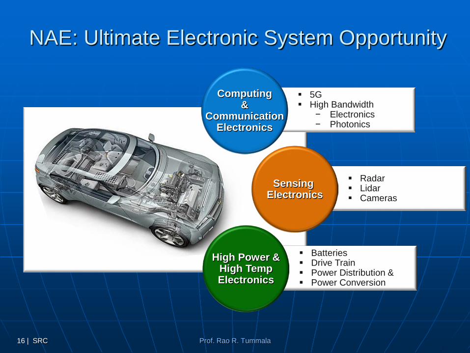
NAE: Ultimate Electronic System Opportunity
5G High Bandwidth
− Electronics− Photonics
Computing&
CommunicationElectronics
Radar Lidar Cameras
Sensing Electronics
Batteries Drive Train Power Distribution & Power Conversion
High Power &High TempElectronics

17 | SRC Prof. Rao R. Tummala
Global Ecosystem for NAE –From R&D to System Integration
Research and Development
Supply Chain Materials and Tools
Devices, Components & Substrates
Components
Functional Integration
OEMs

18 | SRC Prof. Rao R. Tummala
INDUSTRY CONSORTIUM AT GT

19 | SRC Prof. Rao R. Tummala
Georgia Tech Industry Consortium
Uniqueness of GT PRC
Technical Strategy
Faculty Expertise
State of Micro-
electronics
Industry Partnership
300mm Cleanroom
Pilot Facility

20 | SRC Prof. Rao R. Tummala
Automotive Programs in the South EastOrganization Emphasis
NTRC – National Transportation Research Center, Oak Ridge, TN
Improving fuel economy, reducing emissions and addressing transportation systems issues
CTR – Center for Transportation Research, Univ. of Tennessee, Knoxville
Conduct research; develop expertise; serve transportation research, service and training needs
CU-ICAR – Clemson Univ. - International Center for Automotive Research
Campus is an automotive ecosystem that helps companies make connections and build relationships
CAVE-3 – Center for Advanced Vehicle and Extreme Environmental Electronics, Auburn Univ.
New technologies for packaging electronics with emphasis on cost, harsh environment and reliability
CAVT – Center for Advanced Vehicle Technologies, Univ. of Alabama, Tuscaloosa
Powertrains, energy storage, materials and manufacturing and other automotive electronics
CAVS – Center for Advance Vehicular Systems, Mississippi St. Univ., Starkville
Engineering solutions for design, technology, production, and infrastructure for sustainable mobility
ATDC – Advanced Technology Development Center, EI2, Georgia Tech
Startup incubator that helps technology entrepreneurs in Georgia launch and grow successful companies
Venture Lab, EI2, Georgia Tech Ranked #2 University based incubator in the worldNCTSPM – National Center for Transportation Systems Productivity and Management; Ga Tech, FL International Univ, Univ. Central FL, Univ. Alabama Birmingham
Tier 1 University Transportation Center (UTC) that conducts transportation related research in the areas of safety, state-of-good-repair, and economic competitiveness

21 | SRC Prof. Rao R. Tummala
Uniqueness of GT Consortium
Leading-edge, precompetitive, 100 global researchers, developers, manufacturers and OEMS
Co-development by all 50+ companies Device-Package synergy and system integration Basic research by Ph.D and MS students Integration and prototype research by GRAs, company
engineers and GT research faculty Long-term roadmap with 2 year deliverables
22 | SRC Prof. Rao R. Tummala
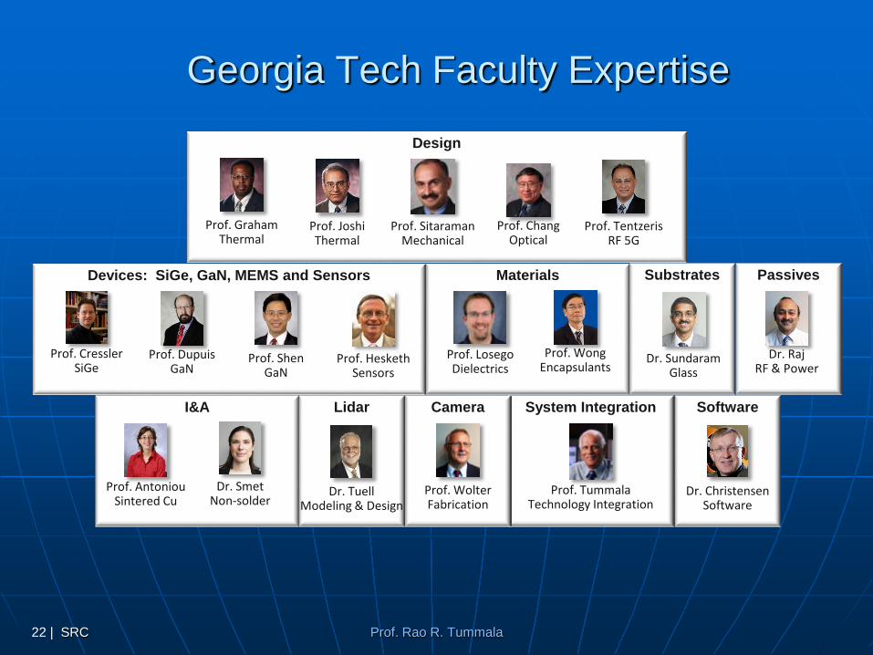
Georgia Tech Faculty Expertise Design
Prof. ChangOptical
Prof. SitaramanMechanical
Prof. TentzerisRF 5G
Prof. JoshiThermal
Prof. GrahamThermal
Devices: SiGe, GaN, MEMS and Sensors
Prof. ShenGaN
Prof. CresslerSiGe
Prof. DupuisGaN
Prof. HeskethSensors
Materials
Prof. LosegoDielectrics
Prof. WongEncapsulants
Substrates
Dr. SundaramGlass
Passives
Dr. RajRF & Power
I&A
Prof. AntoniouSintered Cu
Dr. SmetNon-solder
System Integration
Prof. TummalaTechnology Integration
Camera
Prof. WolterFabrication
Software
Dr. ChristensenSoftware
Lidar
Dr. TuellModeling & Design

23 | SRC Prof. Rao R. Tummala
Environmental Testing Shared User Labs
Plating Facility Substrate Cleanroom Assembly Facility
300mm Cleanroom Pilot Facility and Labs

24 | SRC Prof. Rao R. Tummala
ESI Cornerstone Laser MKS Ozone Cleaner K&S APAMA Bonder
Disco Dicing Saw and Planer XYZTEC Bond Tester
Partnership with Tool Companies
Ushio Projection Lithography
25 | SRC Prof. Rao R. Tummala
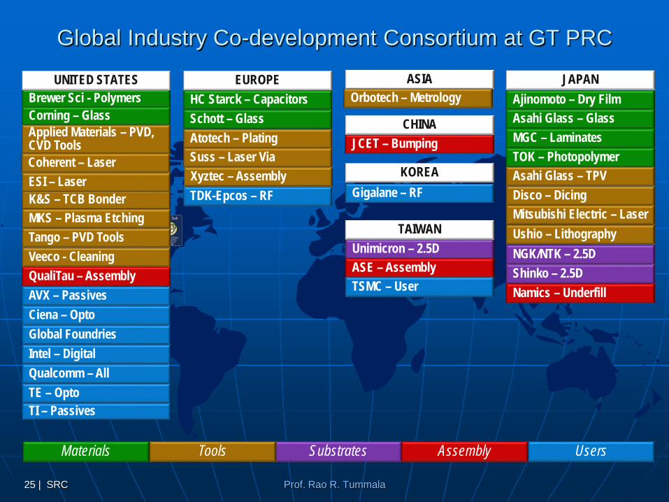
Global Industry Co-development Consortium at GT PRC
Asahi Glass – GlassAjinomoto – Dry Film
MGC – Laminates TOK – Photopolymer
Schott – GlassHC Starck – Capacitors
Corning – Glass Brewer Sci - Polymers
Materials
Shinko – 2.5DNGK/NTK – 2.5D Unimicron – 2.5D
Substrates
Namics – Underfill
ASE – Assembly
JCET – Bumping
QualiTau – Assembly
Assembly
TDK-Epcos – RF
Qualcomm – All TE – Opto
AVX – Passives
TI – Passives
TSMC – User
Gigalane – RF
Users
Ciena – Opto Global FoundriesIntel – Digital
JAPANEUROPEUNITED STATES
TAIWAN
CHINA
KOREA
ASIA
Asahi Glass – TPV
Mitsubishi Electric – Laser Ushio – Lithography
Disco – Dicing
Atotech – Plating Suss – Laser ViaCoherent – Laser
Tango – PVD Tools
Applied Materials – PVD, CVD Tools
K&S – TCB Bonder
Veeco - Cleaning
MKS – Plasma Etching
Tools
ESI – Laser Xyztec – Assembly
Orbotech – Metrology

26 | SRC Prof. Rao R. Tummala
Additional Recent Industry Interest
KOREASamsung
JAPAN
IbidenFujiFilm
RenesasNitto Denko
RohmWALTS
EUROPE
Thales
BoschAudi
Continental
HeraeusInfineon
Hella
ValeoVolkswagen
UNITED STATES
Veeco
DowAMD
Finisar
On-Semi
Stellar
Linear
Rudolph
USCI
Savansys
Rodgers
IDT

27 | SRC Prof. Rao R. Tummala
GT PRC 2016 Industry Consortia Members

28 | SRC Prof. Rao R. Tummala
Fundamental Challenges & Trends in Electronics
1. ICsICs
IC < 14nm: no cost Front end: leakage Back end: RC delay Split SOC inevitable
Device Packaging
Digital: Organic, Si RF: LTCC & laminate Power: embedded
fanout Bulky and expensive
Systems Packaging
SIP MCM 2.5D Interposers with
3D ICs
Trend: 2.5D Si Interposer 2.5D Glass BGA
(GT)
Trend: WLFO PFO: Glass by GT
Trend:System on Board 3D System
Architecture (GT)

29 | SRC Prof. Rao R. Tummala
1970s
Leadframe
1980s
Ceramics
1990s
Build-up Laminate & WLP
GlassPackaging
Wafer Packaging WLP WLFO Si Interposer
Packaging Evolution to Glass Pkg, & Wafer Fanout
Chip-first and Chip-last Panel Fanout Glass
Packaging

30 | SRC Prof. Rao R. Tummala
Wafer vs. Panel Fanout
Wafer FO: Promise of Ultimate I/O Density• Reality: Limited by materials and processes• Limited to 300 mm so limited to small size packages• High cost for large multi-chip or SIP• Reliability and lithography limited by molding materials• One-stop shop for IC and package
Panel FO: Promise of Ultimate Low Cost• Reality: Low cost• Limited in I/O density• Limited by polymer materials• Limited by large area sub-micron tools• Limited by large panel foundry investments
Future: Ultimate I/O Density and Ultimate Low Cost!

31 | SRC Prof. Rao R. Tummala
GT Industry Consortium Technical Strategy
2.5D Glass Interposer
3D GlassPhotonicsGlass
Fanout
Radar
Lidar
3D StereoCamera
5G & mm-wave
Power(Low &
Wireless)
RF(WLAN &
LTE)
High TempMaterial & Reliability
High Power& Reliability
ResearchFocus

32 | SRC Prof. Rao R. Tummala
Basic & Design & Demonstration Research (2016-'18)
8. High-temp Electronic Materials High-temp polymers High-temp passives High-temp interconnections High-temp encapsulants
5. Interconnects & Assembly SLID bonding Low-temp Cu-Cu interconnects High-throughput TCB Direct-SMT of Glass BGA Pre-applied underfill
7. High-power/High-speedSwitch and Gate DriverMetal Insulator substratesEmbedded power chips & passivesSintered-Cu interconnection
2. Electronic SubstratesHigh-temp TPVs1µm RDLsTPV & RDL reliability
3. Photonic Substrates Single and multi-mode Optical vias WG and turning structures Fiber coupling
6. Devices GaN,SiC, SiGe, MEMS and
Sensors OEIC, RF ICs, and Digital ICs
1. Design Electrical: signal & power
integrity Mechanical: warpage & reliability Thermal: Cu TPVs, evaporation
and condensation
D&D Test Vehicles1. Computing & Communications
ElectronicsA. RF (WLAN & LTE)B. Power (Low & WirelessC. 5G and mm-waveD. 2.5D Glass InterposerE. 3D Glass PhotonicsF. Glass Fanout
2. Sensing ElectronicsA. RadarB. LidarC. Camera
3. High-power & High-temp ElectronicsA. High-powerB. High-temperature
4. Components Capacitors Inductors EMI shields PA thermal
Diplexers Antennas Wireless power

33 | SRC Prof. Rao R. Tummala
Si-like I/Os with Glass Packaging
Parameter Prior to 2014 2014-2016 2016-2018TPV• Glass Thickness 180 µm 100µm 30-50µm• TPV Pitch 150-200µm 100-120µm 50µmRDL• Line- Space- Via 5-5-15µm 3-3-8µm 1.5-1.5-2µm• Layer Count 2 + 2 3 + 3 4 + 4
Dr. SundaramProf. Tummala

34 | SRC Prof. Rao R. Tummala
What is a System Scaling Platform?Ultra-thin Panel Glass with Ultra-fine Pitch TPV & RDL
Good Fair Poor
Ideal PropertiesMaterials
Glass SC Si Organic Metal CeramicPoly SiCharacteristic
Electrical
Physical
Thermal
Mechanical
Chemical
TPV and RDL CostReliability
Cost/mm2
High resistivity Low loss and low k Smooth surface finish Large area availability Ultra thin High Conductivity
High strength & modulus Low warpage Resistance to process
chemicals Low cost Via formation
and metallization CTE matched to Si and
PWB At 25µm I/O pitch

35 | SRC Prof. Rao R. Tummala
2um RDL @ 20-40um Pitch
Single Mode Photonics Integration
Leading Advances in Glass Packaging
Multilayer Glass Substrate POR
TPVs in Glass @ TSV Pitch
40um
20um
10um
Glass
Pitch 20um
1st Demo at 20um Pitch 2.5D with 40um Pitch
Dr. SundaramProf. Tummala
36 | SRC Prof. Rao R. Tummala
Si-like RDL on Glass Panels for Low Cost
Dry film resistwet processing
2.0 μm L/S 1.5 μm L/S
Extending SAP to 40 μm Pitch & Beyond Enabled by Glass
Via in Line at 20 μm Pitch Multilayer RDL - 1st time on Panel
Dr. SundaramProf. Tummala

37 | SRC Prof. Rao R. Tummala
Georgia Tech Glass Embedded FanoutSi-like I/Os, Laminate-like Cost
IPDGaAs ICGlass
Silicon-like RDL
1.92 um space
2µm lines and vias
Ultra-fine Pitch I/Os
Same Cost as Laminate Panel
Direct Attach to Board with Reliability
Ultra-thin
No Molding Compound
Ultra-low Loss up to mm-wave
Reduced Die Shift
+/-1um Registration
Hermetics
38 | SRC Prof. Rao R. Tummala
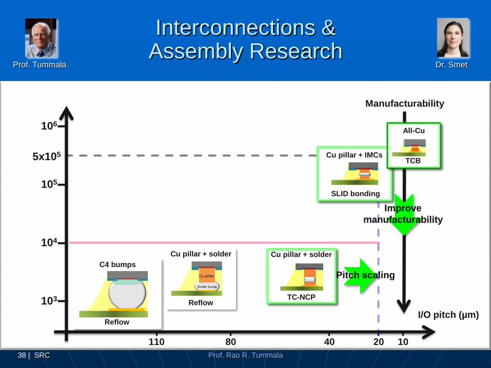
Interconnections & Assembly Research
I/O pitch (µm)
10110 80 40
Reflow
C4 bumps
Reflow
Cu pillar + solder
TC-NCP
Cu pillar + solder
105
104
106
103
5x10⁵
TC-NCP
Cu pillar + solder
Pitch scaling
Manufacturability
Improve manufacturability
SLID bonding
Cu pillar + IMCs
SLID bonding
Cu pillar + IMCs
All-Cu
TCB
All-Cu
TCB
20
Dr. SmetProf. Tummala

39 | SRC Prof. Rao R. Tummala
RF Components & Modules Research
Materials design and synthesis for better properties
Nanoparticles Nanofilms Polymer films
Thinfilm components with better performance & precision
Passive integration on substrates
Passive with Actives to form modulesDiplexerPA Filter
Switch Filter
Glass
PCB
Dr. RajProf. Tummala

40 | SRC Prof. Rao R. Tummala
Power Module Research
Design and demonstrate low power module for consumer electronics with following attributes
State-of-the-art power module PRC’s proposed power module
Miniaturized High Power Handling Low Cost
Dr. RajProf. Tummala Dr. Sharma

41 | SRC Prof. Rao R. Tummala
5G Research
Explore novel designs, materials, processes and 3D packaging structures and RF components to build 5G-enabled modules that accommodate V2X applications with superiority over LTCC and organic packages in terms of:1. Performance2. Miniaturization3. Reliability 4. Cost5. Integrability (e.g.transparent)6. IoT compatibility7. Broadband/multiband
(e.g. 5.9GHz/mmW) operability
Chip-lastPA Rec ICTrans IC
Glass
Controller
PCB
Chip-first
Dr. SundaramProf. Tummala Dr. RajProf. Tentzeris

42 | SRC Prof. Rao R. Tummala
3D GlassPhotonics Research
Demonstration of low loss optical interconnects integrated with high speed electronics in 3D Glass Photonics (3DGP) interposer for optimum Energy Efficiency, Density, and Cost
Si PIC Driver
SMF
Dr. SundaramProf. Chang Dr. Liu

43 | SRC Prof. Rao R. Tummala
mm-Wave AutomotiveRadar Research
Objectives:• Extended Range (Low SNR) by
LNA• chip-package Synergy• SiGe for high speed and Si Mfg.• Board-Level Reliability• Low-cost
Three Focus Areas• Device Innovation• Package Innovation• Chip-Package Co-Development
Short, Medium and Long Range RADAR Modules Critical to Fully Autonomous Driving
Dr. SundaramProf. Cressler Prof. Tummala

44 | SRC Prof. Rao R. Tummala
Lidar Research
Design and demonstrate a 3D Glass Packaging platform for waveform-resolved Lidar module to support integrated collision avoidance
Ability to see through fog/dust/rain/snow. Electrically steerable optical transmitter & receiver array enables high
spatial and temporal resolution Smaller form factor for flexible integration (50x50x20) mm3 Reaction time: ~1 msec High reliability due to solid-state Lidar system
Dr. TuellProf. Wolter

45 | SRC Prof. Rao R. Tummala
Camera Research
Design and demonstrate most advanced and miniaturized mono and high speed stereo camera with integrated image processing.
Reaction time: 1 msec High frame rate on demand: 1000 fps Optional wireless data transmission using Wi-Fi and Bluetooth Low cost and High Reliability for operation time up to 20,000 hours
Prof. HeskethProf. Wolter

46 | SRC Prof. Rao R. Tummala
Design for high-temperature (<250°C), Hi-Rel.: Glass Power Embedding
Integrated power, control and drive → ultra-thin CTE-matched “zero-stress” 3D integration Low thermal impedance, no liquid cooling Low cost
3D IPD
Driver
Thin film
insulator
High-temp glass substrate
Gate driver
Power switch Power diode
Heat sink
Low-cost sintered
interconnections
Microcontroller
µ-controller
Low-CTE & High Thermal Conductivity
High Power & High-temp Electronics Research
Dr. SmetDr. RajProf. DupuisProf. Joshi Prof. Shen

47 | SRC Prof. Rao R. Tummala
Summary
NAE is the Most Complex Electronics System, Requiring:• Technologies and Educated Workforce• Partnership with
Manufacturing Supply-chain and OEMs Georgia Tech Large-scale Global Industry Consortium
Involves about 100:• Researchers• Developers• Manufacturers, and • OEMs