Embed Size (px)
Citation preview
0278-0070 (c) 2016 IEEE. Personal use is permitted, but republication/redistribution requires IEEE permission. See http://www.ieee.org/publications_standards/publications/rights/index.html for more information.
This article has been accepted for publication in a future issue of this journal, but has not been fully edited. Content may change prior to final publication. Citation information: DOI 10.1109/TCAD.2016.2611506, IEEETransactions on Computer-Aided Design of Integrated Circuits and Systems
IEEE TRANSACTIONS ON COMPUTER-AIDED DESIGN OF INTEGRATED CIRCUITS AND SYSTEMS, VOL. XX, NO. X, FEBRUARY 2016 1
System-Level Optimization of AcceleratorLocal Memory for Heterogeneous Systems-on-Chip
Christian Pilato, Member, IEEE, Paolo Mantovani, Student Member, IEEE,Giuseppe Di Guglielmo, Member, IEEE, Luca P. Carloni, Senior Member, IEEE
Abstract—In modern System-on-Chip (SoC) architectures, spe-cialized accelerators are increasingly used to improve perfor-mance and energy efficiency. The growing complexity of these sys-tems requires the use of system-level design methodologies featur-ing high-level synthesis (HLS) for generating these componentsefficiently. Existing HLS tools, however, have limited support forthe system-level optimization of memory elements, which typi-cally occupy most of the accelerator area. We present a completemethodology for designing the private local memories (PLMs) ofmultiple accelerators. Based on the memory requirements of eachaccelerator, our methodology automatically determines an area-efficient architecture for the PLMs to guarantee performance andreduce the memory cost based on technology-related information.We implemented a prototype tool, called MNEMOSYNE, thatembodies our methodology within a commercial HLS flow. Wedesigned thirteen complex accelerators for selected applicationsfrom two recently-released benchmark suites (PERFECT andCORTEXSUITE). With our approach we are able to reduce thememory cost of single accelerators by up to 45%. Moreover,when reusing memory IPs across accelerators, we achieve areasavings that range between 17% and 55% compared to the casewhere the PLMs are designed separately.
Index Terms—Hardware Accelerator, High-Level Synthesis,Memory Design, Multi-bank Architecture.
I. INTRODUCTION
SYSTEM-ON-CHIP (SoC) architectures increasingly fea-ture hardware accelerators to achieve energy-efficient
high performance [1]. Complex applications leverage thesespecialized components to improve the execution of selectedcomputational kernels [2], [3]. For example, hardware acceler-ators for machine learning applications are increasingly used toidentify underlying relations in massive unstructured data [4],[5], [6]. Many of these algorithms first build an internal modelby analyzing very large data sets; then, they leverage thismodel to perform decisions (e.g. to give suggestions to theusers). Thanks to the inherent parallelism of their kernels, theyare good candidates for hardware specialization, especiallywith loosely-coupled accelerators (LCAs) [7], [8], [9].
Manuscript received February 12, 2015; revised June 11, 2016; acceptedAugust 24, 2016. This paper was recommended by Associate Editor L. Benini.This work was supported in part by C-FAR, one of the six centers of STARnet,the DARPA PERFECT program (Contract No: HR0011-13-C-0003), and theNSF (A#: 1219001 and 1527821).
C. Pilato was with Columbia University, New York, NY 10027 USA, andhe is now with the University of Lugano, Lugano 6900, Switzerland (email:[email protected]).
P. Mantovani, G. Di Guglielmo and L.P. Carloni are withColumbia University, New York, NY 10027, USA (e-mail:{paolo,giuseppe,luca}@cs.columbia.edu).
Accelerator LogicMemory Subsystem
Syst
emIn
terc
on
nec
tc
PLM
input
compute 1
output
compute 2
memory interfaces
Inte
rfac
e
Bank
Bank
Bank
Bank
input
output
compute
memory interfaces
Inte
rfac
e
Bank
Bank
PLMProcessor Core
DRAMPLMelements
PLMelements
Accelerator Logic
SoC
DM
A C
trl
DM
A C
trl
Co
nf
Re
gsC
on
fR
egs
Device Driver
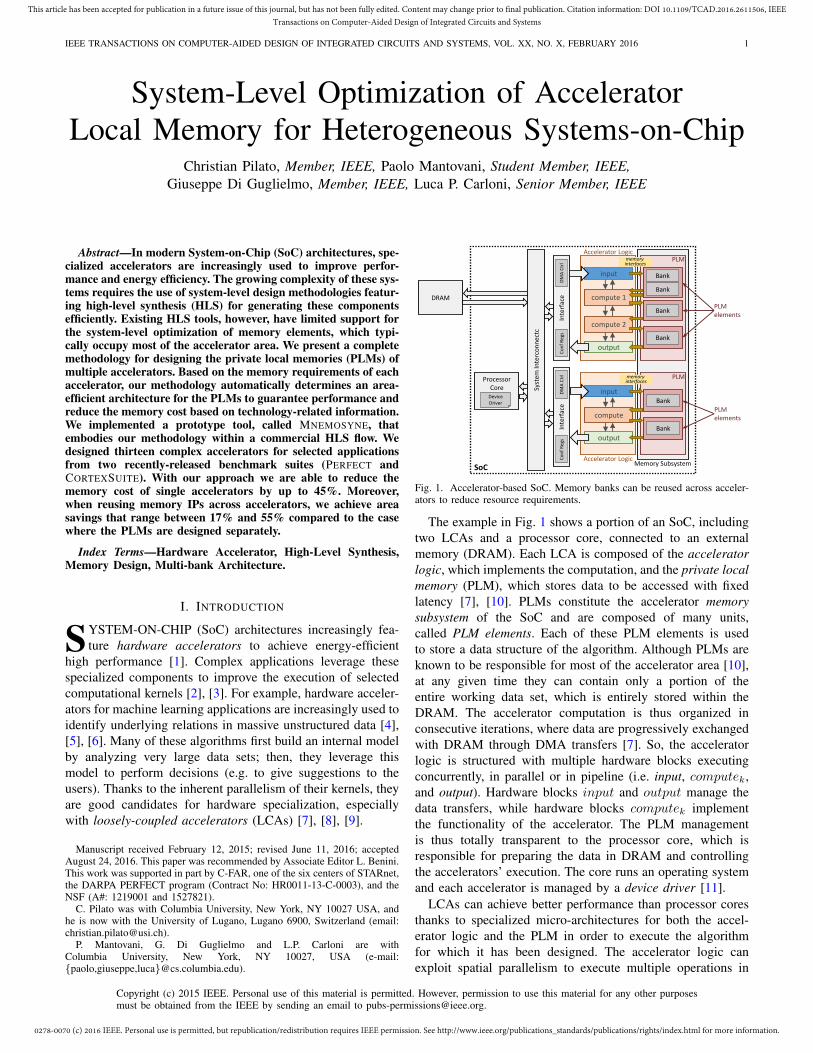
Fig. 1. Accelerator-based SoC. Memory banks can be reused across acceler-ators to reduce resource requirements.
The example in Fig. 1 shows a portion of an SoC, includingtwo LCAs and a processor core, connected to an externalmemory (DRAM). Each LCA is composed of the acceleratorlogic, which implements the computation, and the private localmemory (PLM), which stores data to be accessed with fixedlatency [7], [10]. PLMs constitute the accelerator memorysubsystem of the SoC and are composed of many units,called PLM elements. Each of these PLM elements is usedto store a data structure of the algorithm. Although PLMs areknown to be responsible for most of the accelerator area [10],at any given time they can contain only a portion of theentire working data set, which is entirely stored within theDRAM. The accelerator computation is thus organized inconsecutive iterations, where data are progressively exchangedwith DRAM through DMA transfers [7]. So, the acceleratorlogic is structured with multiple hardware blocks executingconcurrently, in parallel or in pipeline (i.e. input, computek,and output). Hardware blocks input and output manage thedata transfers, while hardware blocks computek implementthe functionality of the accelerator. The PLM managementis thus totally transparent to the processor core, which isresponsible for preparing the data in DRAM and controllingthe accelerators’ execution. The core runs an operating systemand each accelerator is managed by a device driver [11].
LCAs can achieve better performance than processor coresthanks to specialized micro-architectures for both the accel-erator logic and the PLM in order to execute the algorithmfor which it has been designed. The accelerator logic canexploit spatial parallelism to execute multiple operations in
Copyright (c) 2015 IEEE. Personal use of this material is permitted. However, permission to use this material for any other purposesmust be obtained from the IEEE by sending an email to [email protected].
0278-0070 (c) 2016 IEEE. Personal use is permitted, but republication/redistribution requires IEEE permission. See http://www.ieee.org/publications_standards/publications/rights/index.html for more information.
This article has been accepted for publication in a future issue of this journal, but has not been fully edited. Content may change prior to final publication. Citation information: DOI 10.1109/TCAD.2016.2611506, IEEETransactions on Computer-Aided Design of Integrated Circuits and Systems
IEEE TRANSACTIONS ON COMPUTER-AIDED DESIGN OF INTEGRATED CIRCUITS AND SYSTEMS, VOL. XX, NO. X, FEBRUARY 2016 2
parallel. The size of each PLM element is customized withrespect to the amount of data to be stored. Additionally,while processor memories are designed for sequential access(even in case of memory sharing with the accelerator [12],[13]), PLMs require multiple ports to allow the acceleratorlogic to perform multiple memory operations within the sameclock cycle and increase the hardware parallelism. There aredifferent solutions to implement multi-port memories [14].Distributed registers, which are completely contained into theaccelerator logic, are used for small and frequently accesseddata structures. However, the aggregated size of these registersis known to grow exponentially with the amount of datato be stored. Large and complex data structures require theallocation of dedicated memory Intellectual Property (IP)blocks, which are more resource efficient. However, since thesize of these memory elements grows quadratically with thenumber of ports [15], only single- or dual-port memory IPsare usually offered by technology providers [16]. The availablememory IPs compose the so-called memory library, whereeach of them is characterized in terms of height, width, andresource requirements. For example, a variable number ofStatic Random-Access Memories (SRAMs) are available instandard cell-based designs. Block Random-Access Memories(BRAMs) are used instead when targeting FPGA technologies,which have a certain number of such configurable blocksavailable in each device (e.g. between 1,500 and 4,000 16KbBRAMs in modern Xilinx Virtex-7 FPGAs [17]). Each PLMelement is then implemented with a multi-bank architecture,based on the combined requirements of each hardware blockaccessing the corresponding data structure. For example, inthe first accelerator of Fig. 1, hardware blocks input andcompute1 communicate through a data structure; at each clockcycle, input updates one value with one memory-write inter-face, while compute1 elaborates two values with two distinctmemory-read interfaces. To manage these three concurrentmemory operations, the corresponding PLM element musthave two dual-port banks.
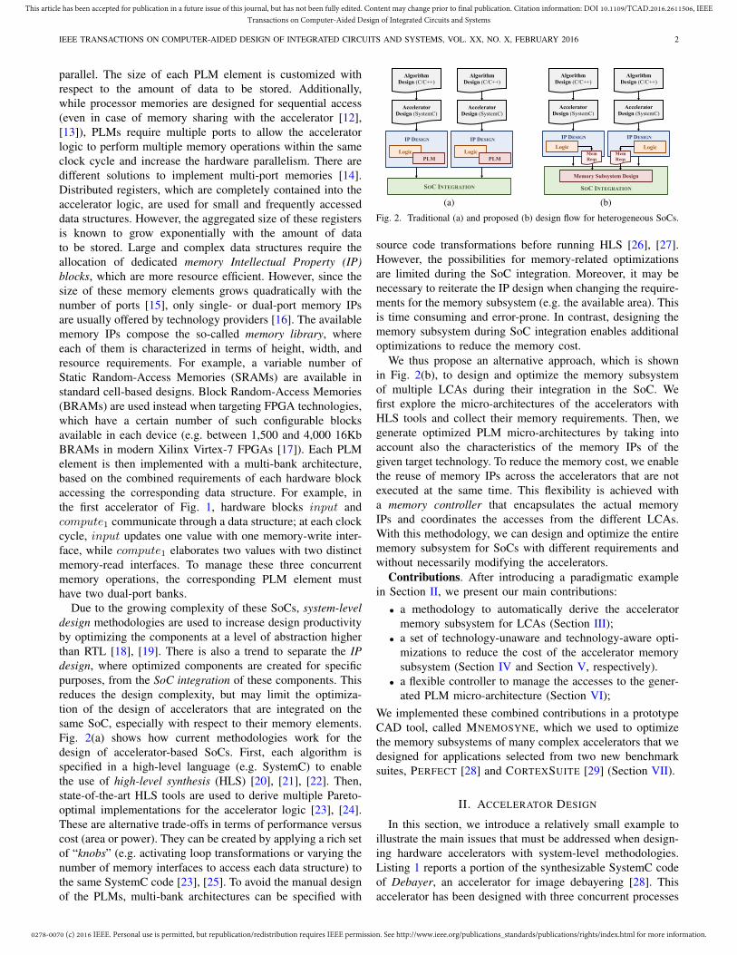
Due to the growing complexity of these SoCs, system-leveldesign methodologies are used to increase design productivityby optimizing the components at a level of abstraction higherthan RTL [18], [19]. There is also a trend to separate the IPdesign, where optimized components are created for specificpurposes, from the SoC integration of these components. Thisreduces the design complexity, but may limit the optimiza-tion of the design of accelerators that are integrated on thesame SoC, especially with respect to their memory elements.Fig. 2(a) shows how current methodologies work for thedesign of accelerator-based SoCs. First, each algorithm isspecified in a high-level language (e.g. SystemC) to enablethe use of high-level synthesis (HLS) [20], [21], [22]. Then,state-of-the-art HLS tools are used to derive multiple Pareto-optimal implementations for the accelerator logic [23], [24].These are alternative trade-offs in terms of performance versuscost (area or power). They can be created by applying a rich setof “knobs” (e.g. activating loop transformations or varying thenumber of memory interfaces to access each data structure) tothe same SystemC code [23], [25]. To avoid the manual designof the PLMs, multi-bank architectures can be specified with
Logic PLM
IP DESIGN
Logic PLM
IP DESIGN
SOC INTEGRATION
Accelerator Design (SystemC)
Algorithm Design (C/C++)
Accelerator Design (SystemC)
Algorithm Design (C/C++)
(a)
Accelerator Design (SystemC)
Algorithm Design (C/C++)
Logic
IP DESIGN
Accelerator Design (SystemC)
Algorithm Design (C/C++)
SOC INTEGRATION
Memory Subsystem Design
Logic
IP DESIGN
Mem Reqs
Mem Reqs
(b)
Fig. 2. Traditional (a) and proposed (b) design flow for heterogeneous SoCs.
source code transformations before running HLS [26], [27].However, the possibilities for memory-related optimizationsare limited during the SoC integration. Moreover, it may benecessary to reiterate the IP design when changing the require-ments for the memory subsystem (e.g. the available area). Thisis time consuming and error-prone. In contrast, designing thememory subsystem during SoC integration enables additionaloptimizations to reduce the memory cost.
We thus propose an alternative approach, which is shownin Fig. 2(b), to design and optimize the memory subsystemof multiple LCAs during their integration in the SoC. Wefirst explore the micro-architectures of the accelerators withHLS tools and collect their memory requirements. Then, wegenerate optimized PLM micro-architectures by taking intoaccount also the characteristics of the memory IPs of thegiven target technology. To reduce the memory cost, we enablethe reuse of memory IPs across the accelerators that are notexecuted at the same time. This flexibility is achieved witha memory controller that encapsulates the actual memoryIPs and coordinates the accesses from the different LCAs.With this methodology, we can design and optimize the entirememory subsystem for SoCs with different requirements andwithout necessarily modifying the accelerators.
Contributions. After introducing a paradigmatic examplein Section II, we present our main contributions:• a methodology to automatically derive the accelerator
memory subsystem for LCAs (Section III);• a set of technology-unaware and technology-aware opti-
mizations to reduce the cost of the accelerator memorysubsystem (Section IV and Section V, respectively).
• a flexible controller to manage the accesses to the gener-ated PLM micro-architecture (Section VI);
We implemented these combined contributions in a prototypeCAD tool, called MNEMOSYNE, which we used to optimizethe memory subsystems of many complex accelerators that wedesigned for applications selected from two new benchmarksuites, PERFECT [28] and CORTEXSUITE [29] (Section VII).
II. ACCELERATOR DESIGN
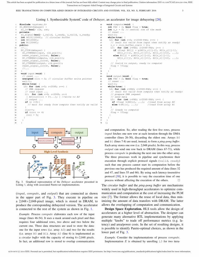
In this section, we introduce a relatively small example toillustrate the main issues that must be addressed when design-ing hardware accelerators with system-level methodologies.Listing 1 reports a portion of the synthesizable SystemC codeof Debayer, an accelerator for image debayering [28]. Thisaccelerator has been designed with three concurrent processes
0278-0070 (c) 2016 IEEE. Personal use is permitted, but republication/redistribution requires IEEE permission. See http://www.ieee.org/publications_standards/publications/rights/index.html for more information.
This article has been accepted for publication in a future issue of this journal, but has not been fully edited. Content may change prior to final publication. Citation information: DOI 10.1109/TCAD.2016.2611506, IEEETransactions on Computer-Aided Design of Integrated Circuits and Systems
IEEE TRANSACTIONS ON COMPUTER-AIDED DESIGN OF INTEGRATED CIRCUITS AND SYSTEMS, VOL. XX, NO. X, FEBRUARY 2016 3
Listing 1. Synthesizable SystemC code of Debayer, an accelerator for image debayering [28].1 #include <systemc.h>2 SC_MODULE(Debayer) {3 sc_in<bool> clk, rst;4 private:5 sc_signal<bool> i_valid, i_ready, o_valid, o_ready;6 int A0[6][2048]; // circular buffer7 int B0[2048];8 int B1[2048];9 public:
10 //...11 SC_CTOR(debayer) {12 SC_CTHREAD(input, clk.pos());13 reset_signal_is(rst, false);14 SC_CTHREAD(compute, clk.pos());15 reset_signal_is(rst, false);16 SC_CTHREAD(output, clk.pos());17 reset_signal_is(rst, false);18 //...19 }20 void input(void) {21 // reset ...22 unsigned circ = 0; // circular buffer write pointer23 wait();24 while(true) {25 L0: for (int r=0; r<2048; r++) {26 // DMA request27 // read input ...28 L1: for (int c=0; c<2048; c++)29 { A0[circ][c] = f(...); } //write to A030 // output ...31 if (r >=5){32 // wait for ready from compute then notify as valid33 }34 circ++;35 if (circ == 6)36 circ = 0;37 }38 }39 }
40 void compute(void) {41 int PAD = 2; bool flag = true;42 int r_r = 0; // central row of the mask43 // reset ...44 wait();45 while(true) {46 L2: for (int r=0; r<2048-PAD; r++) {47 // (wait for valid from input then notify as ready)48 r_r = circ_buffer_row(r + 2);49 L3: for (int j=PAD; j<2048-PAD; j++) {50 if (flag) B0[j] = g(A0[r_r][j-2], A0[r_r][j-1],51 A0[r_r][j], A0[r_r][j+1], A0[r_r][j+2], ...);52 else B1[j] = g(A0[r_r][j-2], A0[r_r][j-1],53 A0[r_r][j], A0[r_r][j+1], A0[r_r][j+2], ...);54 }55 // (valid to output, ready to compute)56 flag = !flag;57 }58 }59 }60 void output(void) {61 int PAD = 2; bool flag = true;62 // reset ...63 wait();64 while(true) {65 L4: for (int r=PAD; r<2048-PAD; r++) {66 // (wait for valid from compute then notify as ready)67 // prepare DMA request68 // send data69 L5: for (int c=PAD; c<2048-PAD; c++) {70 if (flag) h(B0[c], ...); //read from array B071 else h(B1[c], ...); //read from array B172 }73 // (ready to compute)74 flag = !flag;75 }76 }77 }78 };
outputinput compute
B0[2048]A0[6][2048]
High-Level Synthesis
late
ncy
area
late
ncy
area
late
ncy
area
A0 – 2R
B0 – 1W
B1 – 1W
A0 – 2R
B0 – 1W
B1 – 1W
A0 – 6R
B0 – 1W
B1 – 1W
A
B
C
A0 – 2W A0 – 4R
B0 – 1W
B1 – 1W
B0 – 1R
B1 – 1R
D
E
G
F
HI
L
M
A0 – 1W
A0 – 4W
B1[2048]
Fig. 3. Graphical representation of the Debayer accelerator presented inListing 1, along with associated Pareto-set implementations.
(input, compute, and output) that are connected as shownin the upper part of Fig. 3. They execute in pipeline ona 2,048×2,048-pixel image, which is stored in DRAM, toproduce the corresponding debayered version. The acceleratoris connected to the rest of the system as shown in Fig. 1.
Example. Process compute elaborates each row of the inputimage (lines 46-54). It uses a mask around each pixel and thusrequires four additional rows, two above and two below thecurrent one. Three data structures are used to store the data:one for the input rows (i.e. array A0) and two for the results(i.e. arrays B0 and B1). Array A0 (line 6) is implemented asa circular buffer with the capacity of storing 6×2,048 pixels.In fact, an additional row is stored to overlap communication
and computation. So, after reading the first five rows, processinput fetches one new row at each iteration through the DMAcontroller (lines 26-30), discarding the oldest one. Arrays B0and B1 (lines 7-8) are used, instead, to form a ping-pong buffer.Each array stores one row (i.e. 2,048 pixels). In this way, processoutput can send one row back to DRAM (lines 67-71), whileprocess compute is producing the next one into the other array.The three processes work in pipeline and synchronize theirexecution through explicit protocol signals (valid, ready)such that one process cannot start its computation before theprevious one has produced the required amount of data (lines 32and 47, and lines 55 and 66). By using such latency-insensitiveprotocol [30], it is possible to vary the execution time of oneprocess without affecting the execution of the others. �
The circular buffer and the ping-pong buffer are mechanismswidely used in high-throughput accelerators to optimize com-munication and computation at the cost of increasing the PLMsize [7]. The former allows the reuse of local data, thus min-imizing the amount of data transfers with DRAM. The latterallows the overlapping of computation and communication.
Design Space Exploration. HLS tools allow the design ofaccelerators at a higher level of abstraction. The designer cangenerate many alternative RTL implementations by applyingmultiple “knobs” to trade off performance metrics (e.g. la-tency) and area/power costs. In the set of resulting designs, itis possible to identify Pareto-optimal choices, as shown in thelower part of Fig. 3.
Example. Consider the implementations of process compute.Implementation E is obtained by unrolling L3 for two itera-
0278-0070 (c) 2016 IEEE. Personal use is permitted, but republication/redistribution requires IEEE permission. See http://www.ieee.org/publications_standards/publications/rights/index.html for more information.
This article has been accepted for publication in a future issue of this journal, but has not been fully edited. Content may change prior to final publication. Citation information: DOI 10.1109/TCAD.2016.2611506, IEEETransactions on Computer-Aided Design of Integrated Circuits and Systems
IEEE TRANSACTIONS ON COMPUTER-AIDED DESIGN OF INTEGRATED CIRCUITS AND SYSTEMS, VOL. XX, NO. X, FEBRUARY 2016 4
tions, which requires two concurrent memory-read operations.Implementation F is obtained by unrolling L3 for four iterationsto maximize performance at the cost of more area, but withonly two memory-read interfaces; this creates a bottleneckbecause the four memory operations cannot be all scheduledin the same clock cycle. Implementation G, which Pareto-dominates implementation F , is obtained by unrolling L3 forfour iterations and having four memory-read interfaces to allowthe four memory-read operations to execute concurrently. �
Accelerator Logic Design. Based on the overall require-ments of the SoC architecture, the designer then selects animplementation for each process to create the final system (i.e.compositional high-level synthesis [23], [24]). CompositionalHLS allows IP designers to optimize the different hardwareblocks separately and more efficiently, but requires that se-lecting an implementation for one block does not imply anychanges to the others. This is critical for shared resources,such as memory elements. In fact, changing the number ofconcurrent memory operations on a data structure sharedbetween two components may impact the memory operationsof the other components.
Example. Assume that implementations A and E are selectedfor processes input and compute, respectively; then, array A0
must be stored in a PLM with one memory-write interface andtwo memory-read interfaces. Instead, if implementation G isselected for process compute, the PLM for storing the samearray requires four memory-read interfaces. �
System-level Memory Optimization. We aim at generatingan optimized memory subsystem for one or more accelerators.The designer provides information on the data structures tobe stored in the PLMs, along with additional information onthe number of memory interfaces for each accelerator and thecompatibilities between the data structures. This information isused to share the memory IPs across accelerators whenever itis possible. Our approach is motivated by the following obser-vations. First, when a data structure is not used, the associatedPLM does not contain any useful data; the correspondingmemory IPs can be reused for storing another data structure,thus reducing the total size of the memory subsystem [10].Second, in some technologies, the area of a single memory IPis smaller than the aggregated area of smaller IPs. For example,in an industrial 32nm CMOS technology, we experimentedthat a 1,024×32 SRAM is almost 40% smaller than the areaof two 512×32 SRAMs, due to the replicated logic for addressdecoding. In these cases, it is possible to store two datastructures in the same memory IP provided that there arenot conflicts on the memory interfaces, i.e. the data structuresare never accessed at the same time with the same memoryoperation. Next, we formalize these situations.
To understand when two data structures can share the samememory IPs, we recall the definition of data structure lifetime.
Definition. The lifetime of a data structure b is the intervaltime between the first memory-write and the last memory-readoperations to the data structure [31]. �
Having two data structures with no overlapping lifetimesmeans that while operating on one data structure the otherremains unused. Hence, we can use the same memory IPs to
HLS and DSE
Accelerator Design1 (SystemC)
Accelerator Logic1 (Verilog)
Memory Requirements1 HLS and DSE
Accelerator Designk (SystemC)
Accelerator Logick (Verilog)
Memory Requirementsk
Compatibility Information Memory
IPs
Technology-unaware Transformations1
Local Tech-aware Transformations1
Memory Subsystem (Verilog)
Global Technology-aware Transformations
1 1
2
3
4
MNEMOSYNE Technology-unaware Transformationsk
2
Local Tech-aware Transformationsk
3
Generation of RTL Architecture 5
…
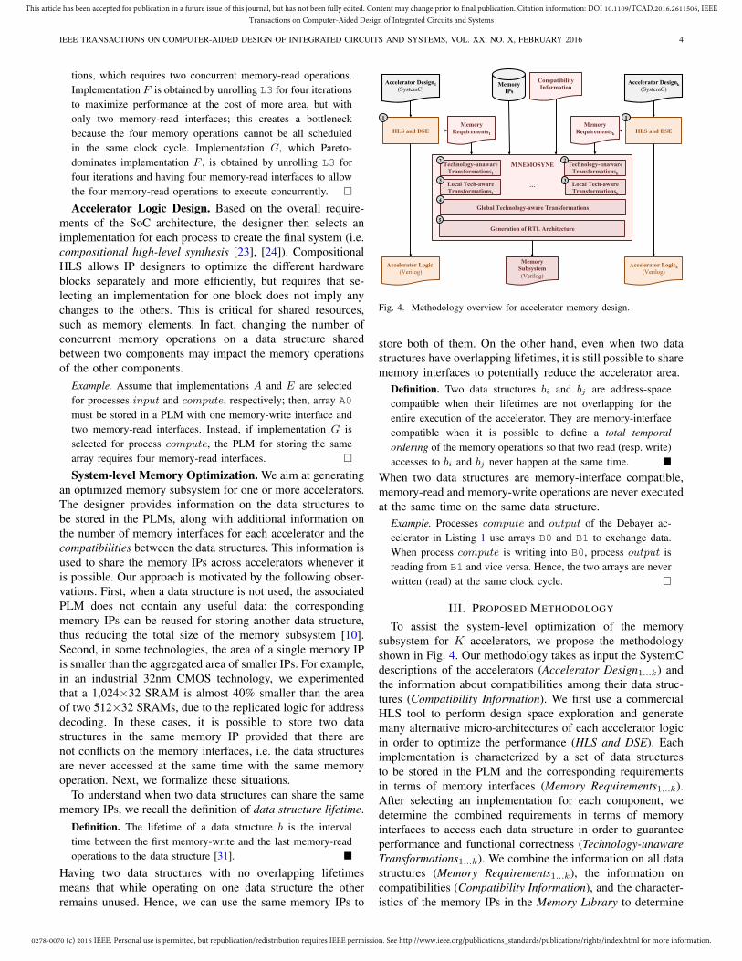
Fig. 4. Methodology overview for accelerator memory design.
store both of them. On the other hand, even when two datastructures have overlapping lifetimes, it is still possible to sharememory interfaces to potentially reduce the accelerator area.
Definition. Two data structures bi and bj are address-spacecompatible when their lifetimes are not overlapping for theentire execution of the accelerator. They are memory-interfacecompatible when it is possible to define a total temporalordering of the memory operations so that two read (resp. write)accesses to bi and bj never happen at the same time. �
When two data structures are memory-interface compatible,memory-read and memory-write operations are never executedat the same time on the same data structure.
Example. Processes compute and output of the Debayer ac-celerator in Listing 1 use arrays B0 and B1 to exchange data.When process compute is writing into B0, process output isreading from B1 and vice versa. Hence, the two arrays are neverwritten (read) at the same clock cycle. �
III. PROPOSED METHODOLOGY
To assist the system-level optimization of the memorysubsystem for K accelerators, we propose the methodologyshown in Fig. 4. Our methodology takes as input the SystemCdescriptions of the accelerators (Accelerator Design1...k) andthe information about compatibilities among their data struc-tures (Compatibility Information). We first use a commercialHLS tool to perform design space exploration and generatemany alternative micro-architectures of each accelerator logicin order to optimize the performance (HLS and DSE). Eachimplementation is characterized by a set of data structuresto be stored in the PLM and the corresponding requirementsin terms of memory interfaces (Memory Requirements1...k).After selecting an implementation for each component, wedetermine the combined requirements in terms of memoryinterfaces to access each data structure in order to guaranteeperformance and functional correctness (Technology-unawareTransformations1...k). We combine the information on all datastructures (Memory Requirements1...k), the information oncompatibilities (Compatibility Information), and the character-istics of the memory IPs in the Memory Library to determine
0278-0070 (c) 2016 IEEE. Personal use is permitted, but republication/redistribution requires IEEE permission. See http://www.ieee.org/publications_standards/publications/rights/index.html for more information.
This article has been accepted for publication in a future issue of this journal, but has not been fully edited. Content may change prior to final publication. Citation information: DOI 10.1109/TCAD.2016.2611506, IEEETransactions on Computer-Aided Design of Integrated Circuits and Systems
IEEE TRANSACTIONS ON COMPUTER-AIDED DESIGN OF INTEGRATED CIRCUITS AND SYSTEMS, VOL. XX, NO. X, FEBRUARY 2016 5
an optimized architecture for each PLM. First, we applytransformations for each accelerator (Local Technology-awareTransformations1...k). Then, we consider all accelerators atthe same time and identify when the memory IPs can bereused across different data structures to minimize the costof the entire memory subsystem (Global Technology-awareTransformations). As output, we produce the RTL descriptionof the memory subsystem (Generation of RTL Architecture)that can be directly integrated with the RTL descriptions ofthe accelerator logic generated by the HLS tool.
We implemented the steps related to memory optimiza-tion (from 2 to 5 of Fig. 4) in a prototype tool, calledMNEMOSYNE. We interfaced MNEMOSYNE with a commer-cial HLS tool to automatically derive the memory requirementsbased on the knobs’ configuration. In the following sections,we describe each of the memory-optimization steps.
IV. TECHNOLOGY-UNAWARE TRANSFORMATIONS
In the HLS phase, the designer applies a set of micro-architectural optimization knobs to trade-off performance andcost for the accelerator logic. The corresponding PLM archi-tecture has then to be designed so that the accelerator behavescorrectly and achieves the desired performance. Specifically,the PLM must provide each data to the accelerator logic inthe number of cycles (usually one) assumed by the HLSscheduling phase. For functional correctness, no more thanone operation must be executed on each port of the memoryIP at the same time (i.e. conflict-free accesses to the banks).It is thus necessary to determine the number of concurrentmemory operations required to access each data structure andthe corresponding number of memory interfaces. These com-bined memory requirements determine the number of parallelblocks required by each data structure to avoid conflicts whenaccessing the banks. To reduce the cost of the entire memorysubsystem, we identify data structures that can be assignedto the same PLM element and share the same memory IPs.So, this logical organization of the physical memory IPs intoparallel blocks can vary from one data structure to the otherof the same PLM element.
Example. Consider two address-space compatible data structuresbi and bj . Each requires one memory-write interface, whilethey require four and two memory-read interfaces, respectively.The PLM element is organized in four parallel blocks for bi;this requires at least four memory IPs, which can be logicallyreorganized in two parallel blocks for bj . �
To identify the minimum number of memory interfaces thatcan access the data at the same time allows us to minimizethe number of parallel blocks and, in turn, of memory IPs.
Example. Assume a 512×32 array to be stored in the PLM.Process input produces the data. Processes compute1 andcompute2 need access to the data with two memory-readinterfaces each. Without any additional information, the arrayrequires four parallel blocks, two for compute1 and two forcompute2. The designer may specify that, by construction,processes compute1 and compute2 never access the data at thesame time (e.g. they execute serially). If so, two parallel blocks
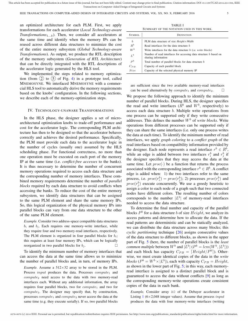
TABLE ISUMMARY OF THE NOTATION USED IN THIS WORK.
SYMBOL DEFINITION
b PLM data structure of size Height×Width
Rb Read interfaces for the data structure b
W b Write interfaces for the data structure b (i.e. write blocks)
Lb Number of read interfaces for accessing data structure b based onsharing information
P b Total number of parallel blocks for data structure b
CPB Capacity of each parallel block
Size Capacity of the selected physical memory IP
are sufficient since the two available memory-read interfacescan be used alternatively by compute1 and compute2. �
We propose the following approach to identify the minimumnumber of parallel blocks. During HLS, the designer specifiesthe read and write interfaces (Rb and W b, respectively) toaccess each data structure b. Multiple write operations fromone process can be supported only if they write consecutiveaddresses. This defines the number W b of write blocks. Writeoperations from different processes can be supported only ifthey can share the same interfaces (i.e. only one process writesthe data at each time). To identify the minimum number of readinterfaces, we apply graph coloring to a conflict graph of theread interfaces based on compatibility information provided bythe designer. Each node represents a read interface rb ∈ Rb,while an edge is added between two interfaces rbi and rbj ifthe designer specifies that they may access the data at thesame time. Let proc(·) be a function that returns the processassociated with the corresponding interface rb ∈ Rb. A conflictedge is added when: 1) the two interfaces refer to the sameprocess, i.e. proc(rbi ) = proc(rbj); 2) processes proc(rbi ) andproc(rbj) execute concurrently. We use a greedy heuristic toassign a color to each node of a graph such that two connectednodes have different colors. The resulting number of colorscorresponds to the number |Lb| of memory-read interfacesneeded to access the data structure.
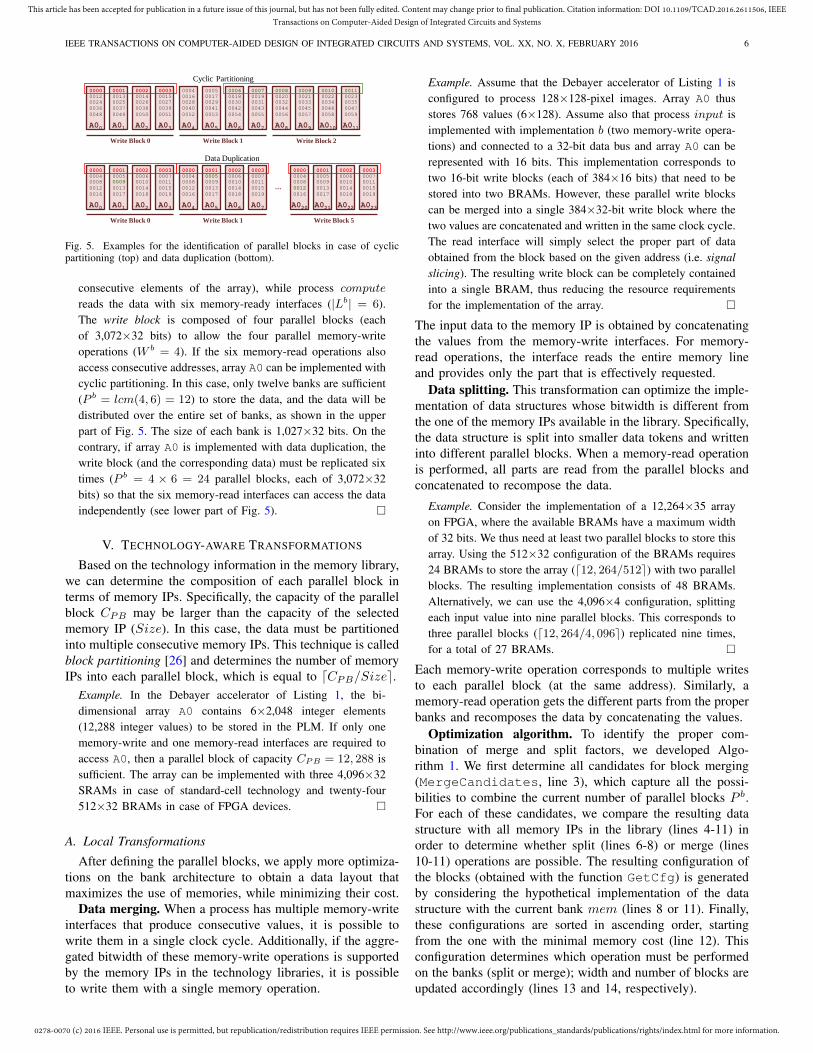
To determine the final number and capacity of the parallelblocks P b for a data structure b of size Height, we analyze itsaccess patterns and determine how to allocate the data. If theread patterns are deterministic and can be statically analyzed,we can distribute the data structure across many blocks; thiscyclic partitioning technique [26] assigns consecutive valuesof the data structure to different blocks, as shown in the upperpart of Fig. 5 (here, the number of parallel blocks is the leastcommon multiple between W b and |Lb| (P b = lcm(W b, |Lb|))and each block has capacity CPB = dHeight/P be). Other-wise, we must create identical copies of the data in the writeblocks (P b =W b×|Lb|), each with capacity CPB = Height,as shown in the lower part of Fig. 5; in this way, each memory-read interface is assigned to a distinct parallel block and isguaranteed to access the data without conflicts [9] as long asthe corresponding memory-write operations create consistentcopies of the data in each bank.
Example. Consider array A0 of the Debayer accelerator inListing 1 (6×2,048 integer values). Assume that process input
produces the data with four memory-write interfaces (writing
0278-0070 (c) 2016 IEEE. Personal use is permitted, but republication/redistribution requires IEEE permission. See http://www.ieee.org/publications_standards/publications/rights/index.html for more information.
This article has been accepted for publication in a future issue of this journal, but has not been fully edited. Content may change prior to final publication. Citation information: DOI 10.1109/TCAD.2016.2611506, IEEETransactions on Computer-Aided Design of Integrated Circuits and Systems
IEEE TRANSACTIONS ON COMPUTER-AIDED DESIGN OF INTEGRATED CIRCUITS AND SYSTEMS, VOL. XX, NO. X, FEBRUARY 2016 6
A04
0000
0004
0008
0012
0016
A05
0001
0005
0009
0013
0017
A06
0002
0006
0010
0014
0018
A07
0003
0007
0011
0015
0019
A020
0000
0004
0008
0012
0016
A021
0001
0005
0009
0013
0017
A022
0002
0006
0010
0014
0018
A023
0003
0007
0011
0015
0019
A00
0000
0004
0008
0012
0016
A01
0001
0005
0009
0013
0017
A02
0002
0006
0010
0014
0018
A03
0003
0007
0011
0015
0019
…
Write Block 0 Write Block 1 Write Block 5
Data Duplication
A04
0004
0016
0028
0040
0052
A05
0005
0017
0029
0041
0053
A06
0006
0018
0030
0042
0054
A07
0007
0019
0031
0043
0055
A08
0008
0020
0032
0044
0056
A09
0009
0021
0033
0045
0057
A010
0010
0022
0034
0046
0058
A011
0011
0023
0035
0047
0059
A00
0000
0012
0024
0036
0048
A01
0001
0013
0025
0037
0049
A02
0002
0014
0026
0038
0050
A03
0003
0015
0027
0039
0051
Write Block 0 Write Block 1 Write Block 2
Cyclic Partitioning
Fig. 5. Examples for the identification of parallel blocks in case of cyclicpartitioning (top) and data duplication (bottom).
consecutive elements of the array), while process compute
reads the data with six memory-ready interfaces (|Lb| = 6).The write block is composed of four parallel blocks (eachof 3,072×32 bits) to allow the four parallel memory-writeoperations (W b = 4). If the six memory-read operations alsoaccess consecutive addresses, array A0 can be implemented withcyclic partitioning. In this case, only twelve banks are sufficient(P b = lcm(4, 6) = 12) to store the data, and the data will bedistributed over the entire set of banks, as shown in the upperpart of Fig. 5. The size of each bank is 1,027×32 bits. On thecontrary, if array A0 is implemented with data duplication, thewrite block (and the corresponding data) must be replicated sixtimes (P b = 4 × 6 = 24 parallel blocks, each of 3,072×32bits) so that the six memory-read interfaces can access the dataindependently (see lower part of Fig. 5). �
V. TECHNOLOGY-AWARE TRANSFORMATIONS
Based on the technology information in the memory library,we can determine the composition of each parallel block interms of memory IPs. Specifically, the capacity of the parallelblock CPB may be larger than the capacity of the selectedmemory IP (Size). In this case, the data must be partitionedinto multiple consecutive memory IPs. This technique is calledblock partitioning [26] and determines the number of memoryIPs into each parallel block, which is equal to dCPB/Sizee.
Example. In the Debayer accelerator of Listing 1, the bi-dimensional array A0 contains 6×2,048 integer elements(12,288 integer values) to be stored in the PLM. If only onememory-write and one memory-read interfaces are required toaccess A0, then a parallel block of capacity CPB = 12, 288 issufficient. The array can be implemented with three 4,096×32SRAMs in case of standard-cell technology and twenty-four512×32 BRAMs in case of FPGA devices. �
A. Local Transformations
After defining the parallel blocks, we apply more optimiza-tions on the bank architecture to obtain a data layout thatmaximizes the use of memories, while minimizing their cost.
Data merging. When a process has multiple memory-writeinterfaces that produce consecutive values, it is possible towrite them in a single clock cycle. Additionally, if the aggre-gated bitwidth of these memory-write operations is supportedby the memory IPs in the technology libraries, it is possibleto write them with a single memory operation.
Example. Assume that the Debayer accelerator of Listing 1 isconfigured to process 128×128-pixel images. Array A0 thusstores 768 values (6×128). Assume also that process input isimplemented with implementation b (two memory-write opera-tions) and connected to a 32-bit data bus and array A0 can berepresented with 16 bits. This implementation corresponds totwo 16-bit write blocks (each of 384×16 bits) that need to bestored into two BRAMs. However, these parallel write blockscan be merged into a single 384×32-bit write block where thetwo values are concatenated and written in the same clock cycle.The read interface will simply select the proper part of dataobtained from the block based on the given address (i.e. signalslicing). The resulting write block can be completely containedinto a single BRAM, thus reducing the resource requirementsfor the implementation of the array. �
The input data to the memory IP is obtained by concatenatingthe values from the memory-write interfaces. For memory-read operations, the interface reads the entire memory lineand provides only the part that is effectively requested.
Data splitting. This transformation can optimize the imple-mentation of data structures whose bitwidth is different fromthe one of the memory IPs available in the library. Specifically,the data structure is split into smaller data tokens and writteninto different parallel blocks. When a memory-read operationis performed, all parts are read from the parallel blocks andconcatenated to recompose the data.
Example. Consider the implementation of a 12,264×35 arrayon FPGA, where the available BRAMs have a maximum widthof 32 bits. We thus need at least two parallel blocks to store thisarray. Using the 512×32 configuration of the BRAMs requires24 BRAMs to store the array (d12, 264/512e) with two parallelblocks. The resulting implementation consists of 48 BRAMs.Alternatively, we can use the 4,096×4 configuration, splittingeach input value into nine parallel blocks. This corresponds tothree parallel blocks (d12, 264/4, 096e) replicated nine times,for a total of 27 BRAMs. �
Each memory-write operation corresponds to multiple writesto each parallel block (at the same address). Similarly, amemory-read operation gets the different parts from the properbanks and recomposes the data by concatenating the values.
Optimization algorithm. To identify the proper com-bination of merge and split factors, we developed Algo-rithm 1. We first determine all candidates for block merging(MergeCandidates, line 3), which capture all the possi-bilities to combine the current number of parallel blocks P b.For each of these candidates, we compare the resulting datastructure with all memory IPs in the library (lines 4-11) inorder to determine whether split (lines 6-8) or merge (lines10-11) operations are possible. The resulting configuration ofthe blocks (obtained with the function GetCfg) is generatedby considering the hypothetical implementation of the datastructure with the current bank mem (lines 8 or 11). Finally,these configurations are sorted in ascending order, startingfrom the one with the minimal memory cost (line 12). Thisconfiguration determines which operation must be performedon the banks (split or merge); width and number of blocks areupdated accordingly (lines 13 and 14, respectively).
0278-0070 (c) 2016 IEEE. Personal use is permitted, but republication/redistribution requires IEEE permission. See http://www.ieee.org/publications_standards/publications/rights/index.html for more information.
This article has been accepted for publication in a future issue of this journal, but has not been fully edited. Content may change prior to final publication. Citation information: DOI 10.1109/TCAD.2016.2611506, IEEETransactions on Computer-Aided Design of Integrated Circuits and Systems
IEEE TRANSACTIONS ON COMPUTER-AIDED DESIGN OF INTEGRATED CIRCUITS AND SYSTEMS, VOL. XX, NO. X, FEBRUARY 2016 7
Algorithm 1: Algorithm to determine merge/split opera-tions to be performed on the parallel blocks.
1 Procedure DetermineBlockOptimization(b, P b, width)Data: b is the buffer to be implementedData: w is the current width of the write blockData: P b is the current configuration of the write blockResult: w is the updated width of the write blockResult: P b is the updated configuration of the write block
2 L← ∅3 foreach m ∈MergeCandidates(P b) do4 foreach mem ∈MemoryLibrary do5 if m == 1 then6 if w > Width(mem) then7 split← dw/Width(mem)e8 L← L ∪ GetCfg(b, P b,mem,w, 1, split)
9 else10 if w ∗m ≥ Width(mem) then11 L← L ∪ GetCfg(b, P b,mem,w,merge, 1)
12 cfg ← GetFirst(OrderByTotalArea(L))13 w ← w ∗ cfg.merge / cfg.split14 P b ← P b ∗ cfg.split / cfg.merge15 return {w, P b}
B. Analysis of Compatibility Information
The compatibility information provided by the designer iscombined into a Memory Compatibility Graph (MCG), whichcaptures the sharing opportunities among the data structures.
Definition. The Memory Compatibility Graph is a graphMCG = (B,E) where each node b ∈ B represents a datastructure to be stored in the entire memory subsystem; anedge e ∈ E connects two nodes when the corresponding datastructures can be assigned to the same physical memory IPs.Each edge e ∈ E is also annotated with the corresponding typeof compatibility (e.g. address-space or memory-interface). �
MCG is the dual of the Memory Exclusion Graph presentedby Desnos et al. [32], which instead contains informationon the data structures that cannot be allocated at the sameaddress space in an MPSoC. A MCG with no compatibilityedges corresponds to implementing each data structure in adedicated PLM element. Increasing the number of edges intothe MCG corresponds to increasing the number of compatibledata structures. This can potentially increase the number ofbanks that can be reused across different data structures.An accurate compatibility graph is the key to optimize thememory subsystem of the accelerators. In most cases, thedesigner has to analyze the application’s behavior or modifythe interconnection topology of the accelerator to increasesharing possibilities.
Identification of Compatibilities. Control signals betweenthe processes can be used to synchronize their execution andvary the lifetime of the data structures, thus increasing thesituations in which it is possible to identify compatibilities.
Example. Assume two computational processes C1 and C2,each having a local 512×32 data structure to store temporaryresults. The standard implementation requires two memoryblocks (e.g. two 512×32 BRAMs) for storing the two datastructures because the two processes may access them at thesame clock cycle. However, we can introduce additional signalsbetween C1 and C2 to serialize the execution so that processC2 can start only when process C1 terminates and process C1
can restart only after process C2 ends. As a result, the two localdata structures have non-overlapping lifetimes and can be storedin the same memory block (e.g. a single 512×32 BRAM). �
Two data structures can also share the memory banks whenthey are always accessed by mutually exclusive parts of theaccelerator’s code. The analyses of the code to be synthesizedcan also identify local data structures of a process that arenever active at the same time, as well as the exact dependencesbetween input and output ones. For example, when differentcomputations are performed based on control conditions, dif-ferent data structures may be read/written; in this case, theycan share the same storage resources because these are alwaysaccessed in mutual exclusion. To identify such compatibilities,the designer has to perform an accurate dataflow analysis atdifferent levels, i.e. both on the accelerator’s interconnectiontopology and on the code of each process. On the other hand, itis also possible to use the following conservative assumptions:
• the lifetime of a data structure shared between two pro-cesses spans from the beginning of the producer executionto the end of the consumer execution; if there are multipleconsumer processes, the termination of the last consumerprocess determines the end of the data structure lifetime.
• local data structures are alive from the beginning to theend of the process, when they store temporary local data,or from the beginning to the end of the entire acceleratorexecution, when they are used to maintain the state.
Moreover, when accelerators are never executed simultane-ously, all data structures belonging to different acceleratorsare address-space compatible with each other. This allows thereuse of memory IPs across multiple accelerators.
Based on the characteristics of the available memory IPs,the designer can decide to implement the data structures in alarger memory IP.
Example. The two memory-interface compatible arrays B0 andB1 of the Debayer accelerator in Listing 1 (each having thesize of 2,048×32 bits) can be implemented in standard-celltechnology with a single 4,096×32 SRAM (with array B1
starting in the second half of the memory block), instead of two2,048×32 SRAMs. In our industrial 32nm CMOS technology,this reduces the memory area by almost 20%. Conversely, inFPGA technologies, BRAMs have a maximum capacity of512×32 bits and we need multiple instances to virtually increasethe size. Since both implementations require 10 BRAMs thereis no difference in using one or the other. �
Memory-interface compatibilities can be also enabled by thedifferent representations used by the designer who implementsthe communication mechanisms in the SystemC design. Forexample, the same ping-pong buffer can be represented as asingle data structure with an offset or as two distinct arrays.
Example. Consider again the Debayer accelerator of Listing 1.The ping-pong buffer between processes compute and output
is implemented with two distinct arrays B0 and B1 (eachcontaining 2,048 integer values) to be accessed independently.However, it can be also represented as a single array, whose sizeis 2×2,048 integer values since it needs to contain both partsat different offsets. Even if the two solutions are functionally
0278-0070 (c) 2016 IEEE. Personal use is permitted, but republication/redistribution requires IEEE permission. See http://www.ieee.org/publications_standards/publications/rights/index.html for more information.
This article has been accepted for publication in a future issue of this journal, but has not been fully edited. Content may change prior to final publication. Citation information: DOI 10.1109/TCAD.2016.2611506, IEEETransactions on Computer-Aided Design of Integrated Circuits and Systems
IEEE TRANSACTIONS ON COMPUTER-AIDED DESIGN OF INTEGRATED CIRCUITS AND SYSTEMS, VOL. XX, NO. X, FEBRUARY 2016 8
Algorithm 2: Algorithm to determine the physical banksrequired to implement each clique.
1 Procedure DeterminePhysicalBanks(Ci)Data: Ci is the clique to be implementedResult: N is number of memory IPs required to implement the cliqueResult: Size is the size of each memory IP
2 Pi ← GetMinParallelBlocks(Ci)3 b← GetFirst(OrderByNumBlocks(Nodes(Ci),Pi))4 N ← GetMinParallelBlocks(b) // current bank number5 Size← 0 // current capacity of each bank6 if IsPartitioned(b) then7 Size← GetDataSize(b) / N8 else9 Size← GetDataSize(b)
10 foreach b ∈ OrderByNumBlocks(Nodes(Ci),Pi) do11 S ← Floor(N/ GetBanks(b))12 if IsPartitioned(b) then13 if GetDataSize(b) / GetBanks(b) > Size ∗ S then14 Size← GetDataSize(b) / (GetBanks(b) ∗S)
15 else16 if GetDataSize(b) > Size ∗ S then17 Size← GetDataSize(b) /S
18 〈N,Size〉 ← SplitBanks(N,Size)19 return 〈N,Size〉
equivalent and the total amount of data to be stored is the same,the first implementation requires two distinct PLM elements. �
With our approach, we use technology-aware information todetermine the best implementation for the data structuresrather than being limited by the way in which the designerdefines them before HLS.
C. Global Transformations
Definition of Memory Subsystem. We target the problemof optimizing the memory subsystem at the system level byidentifying possibilities for reusing banks across different datastructures, even from different accelerators. For doing this, letus first recall the definition of clique.
Definition. A clique Ci of a graph G = (V,E) is a non-emptysubset of nodes (i.e. Ci ⊆ V ) inducing a complete subgraph(not necessarily maximal) of G. �
In our context, each clique Ci of the MCG represents a setof data structures that can share the same physical banks(i.e. a PLM element). Given a clique Ci, each data structureb ∈ Ci is characterized by the minimum number of parallelblocks P b needed to satisfy its combined requirements ofread and write interfaces, as described in Section IV. Thisinformation is used to compute the organization of the memoryarchitecture (in terms of number and characteristics of thephysical banks) for the clique Ci and its cost Ai. We canthus formulate the system-level memory allocation problemas a graph partitioning problem.
Definition. Let MCG = (B,E) be the MCG associated withthe set of data structures B. The optimal memory allocationconsists in finding a partition of B into n disjoint cliques C =(C1, . . . , Cn) of minimum cost. The cost A of a partition is:
A =
n∑i=1
Ai (1)
where Ai is the cost of clique Ci. The cost A of the entirememory subsystem is the value to be minimized. �
Algorithm 2 determines the number of banks and their sizeto efficiently implement each clique Ci. In our implemen-tation, each clique has a homogeneous organization, whereall physical banks have the same size. This has multi-ple advantages: it eases the reorganization of the banks tostore different data structures; it benefits the floorplanningof the modules by enforcing a regular design [33]; and itsimplifies the logic to create the associated memory con-troller. Specifically, for each data structure contained into theclique, we compute its minimum number of parallel blocks(GetMinParallelBlocks) with the approach discussedin Section IV. We sort the data structures in a descendingorder (OrderByNumBlock), from the one that requires themaximum number of parallel blocks to the one with theminimum number. This determines the maximum number ofparallel blocks and, thus, the minimum number of banks thatare required to provide this bandwidth (lines 3-5). We alsodetermine an initial size for these banks based on the dataallocation strategy to be implemented (lines 6-9).
Then, we analyze all data structures following the samedescending order and we seek for opportunities to reuse thebanks. In particular, when a data structure requires a lowernumber of parallel blocks, it can reuse the exceeding ones inseries to virtually increase the capacity of the parallel blocks(lines 11-17). We also check if the data structure can fit intothis new configuration (line 12). If not, the size of the banksis updated accordingly to the data allocation strategy.
Example. Let’s assume that the current number of banks is four(each having size of 128 words) and that we need to store adata structure which has size of 900 integer values, partitionedin three parallel blocks. The existing four banks cannot beredistributed into the parallel blocks and for this reason S = 1
(line 11). Since this organization is not sufficient to store theentire data structure (line 13), each of the four banks is expandedto store 300 integer values (line 14). �
On the other hand, if the banks can be rearranged and reused,it is not necessary to change their size.
Example. Let’s assume that we now have four banks, which havea size of 300 words, and we need to store a data structure of512 integer values, which requires two parallel banks (P = 2)but with data duplication. The four banks can be rearranged intwo blocks of two banks each (S = 2); the two serial banksprovides a virtual capacity of 600 words for each parallel block.Here we can store the data with a serial reorganization of thebanks without any changes to their size (line 16). �
Finally, if the current size is greater than the largest memoryIP of the library, the banks are implemented with the necessarynumber of serial memory IPs (SplitBanks, line 18).
Memory Footprint Minimization. To obtain an efficientsystem-level allocation of the memory elements, we partitionthe MCG in cliques such that the total cost is minimized(see Equation 1). The cost of each clique is computed asthe aggregated requirement of resources (either silicon areaor number of BRAMs) for its implementation. Specifically,we enumerate all admissible cliques and compute the bankorganization for each of them with the above procedure. Basedon the information in the technology library, we associate the
IEEE TRANSACTIONS ON COMPUTER-AIDED DESIGN OF INTEGRATED CIRCUITS AND SYSTEMS, VOL. XX, NO. X, FEBRUARY 2016 9
resulting cost to each clique, which is expressed as µm2 forstandard-cell technologies and as a number of BRAMs forFPGA technologies.
Selecting the best MCG partition can be formulated as aclique partitioning problem, which is NP-hard. The goal is tominimize the memory cost of the system, defined as
MEM =
N∑i=1
Ai ∗ ci (2)
where N is the total number of admissible cliques, Ai is theresource requirement of the clique Ci, while ci is a Booleanvariable that specifies whether the clique is included in thefinal solution or not.
Given each data structure bi and assuming that Ci representsthe set of cliques that contains bi, we need to ensure that thedata structure is contained into only one clique. Hence, foreach data structure bi, we impose the following constraint:
∀bi :∑n∈Ci
cn = 1 (3)
Each of the resulting cliques requires the generation of thelogic to convert the requests from the memory interfaces intothe proper requests to the actual physical banks.
VI. GENERATION OF THE PLM CONTROLLER
This section describes the architecture and the design ofthe flexible memory controller that we use to coordinateaccesses between the accelerator logic and the PLM elementarchitectures that we generate. From the accelerator logic’sviewpoint, each data structure b has a certain number ofmemory interfaces, based on the requirements of the processesthat need to access it. An active request performed by theaccelerator logic on one of these interfaces corresponds toa memory operation on the data structure b. The physicalimplementation of the PLM is transparent to the acceleratorlogic, which simply specifies an offset (logical address) withrespect to the beginning of the data structure.
Based on the organization of the PLM element where thedata structure is stored, two steps must be performed for eachmemory operation: 1) identify which physical bank effectivelycontains the requested data and activate the memory operationonly on that one; and 2) translate the logical address into thecorresponding physical address of the bank.
Example. Let us consider array A0 of the Debayer acceleratorof Listing 1. Let us assume that process compute needs to readthe 6th element of this array. The corresponding read interfacewill have an active request with logical address set to 5 (i.e.A0[5]). If array A0 is implemented with cyclic partitioningover two banks (e.g. implementation E with two parallel reads),this corresponds to reading the third element of the second bank.If cyclic partitioning is performed instead over four banks (e.g.implementation G with four parallel reads), this corresponds toreading the third element of the second bank. Conversely, ifarray A0 is implemented with data duplication, the access willrefer to the sixth element of any of the banks. �
Each memory interface provides five main signals:
CE
W
E
A
D
Q
ATU-B00
CE
W
E
A
D
Q
ATU-B01
A_C
E0
A_W
E0
A_A
0 A
_D0
A_C
E1
A_A
1 A
_Q1
CE
W
E
A
D
Q
ATU-B10
CE
W
E
A D
Q
ATU-B11
B_C
E0
B_W
E0
B_A
0 B
_D0
B_C
E1
B_A
1 B
_Q1
A_C
E2
A_A
2 A
_Q2
S=0 S=1 0x000 0x001
…
0x100 0x101
…
1 00000001
B_A1 = 0x101
CE
W
E
A
D
Q
ATU-B00
CE
W
E
A
D
Q
ATU-B01
A_C
E0
A_W
E0
A_A
0 A
_D0
A_C
E1
A_A
1 A
_Q1
CE
W
E
A
D
Q
ATU-B10
CE
W
E
A D
Q
ATU-B11
B_C
E0
B_W
E0
B_A
0 B
_D0
B_C
E1
B_A
1 B
_Q1
A_C
E2
A_A
2 A
_Q2
S=0 S=0
P=0
0x000 0x002
… P=1
0x001 0x003
…
0 000010 1
A_A2 = 0x003
CE
B
_CE
1
B
_A1
A_C
E2
A_A
2
1 0 1
ATU-B11
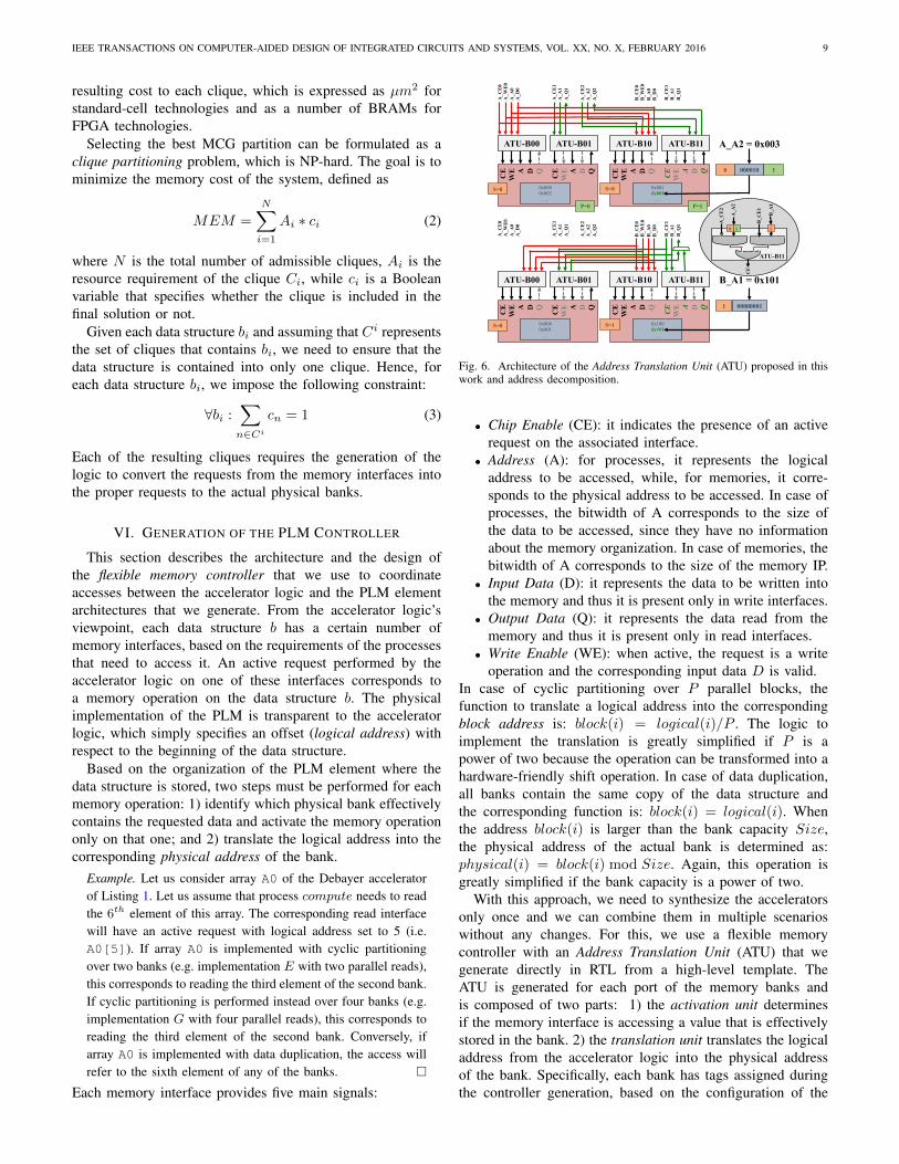
Fig. 6. Architecture of the Address Translation Unit (ATU) proposed in thiswork and address decomposition.
• Chip Enable (CE): it indicates the presence of an activerequest on the associated interface.
• Address (A): for processes, it represents the logicaladdress to be accessed, while, for memories, it corre-sponds to the physical address to be accessed. In case ofprocesses, the bitwidth of A corresponds to the size ofthe data to be accessed, since they have no informationabout the memory organization. In case of memories, thebitwidth of A corresponds to the size of the memory IP.
• Input Data (D): it represents the data to be written intothe memory and thus it is present only in write interfaces.
• Output Data (Q): it represents the data read from thememory and thus it is present only in read interfaces.
• Write Enable (WE): when active, the request is a writeoperation and the corresponding input data D is valid.
In case of cyclic partitioning over P parallel blocks, thefunction to translate a logical address into the correspondingblock address is: block(i) = logical(i)/P . The logic toimplement the translation is greatly simplified if P is apower of two because the operation can be transformed into ahardware-friendly shift operation. In case of data duplication,all banks contain the same copy of the data structure andthe corresponding function is: block(i) = logical(i). Whenthe address block(i) is larger than the bank capacity Size,the physical address of the actual bank is determined as:physical(i) = block(i) mod Size. Again, this operation isgreatly simplified if the bank capacity is a power of two.
With this approach, we need to synthesize the acceleratorsonly once and we can combine them in multiple scenarioswithout any changes. For this, we use a flexible memorycontroller with an Address Translation Unit (ATU) that wegenerate directly in RTL from a high-level template. TheATU is generated for each port of the memory banks andis composed of two parts: 1) the activation unit determinesif the memory interface is accessing a value that is effectivelystored in the bank. 2) the translation unit translates the logicaladdress from the accelerator logic into the physical addressof the bank. Specifically, each bank has tags assigned duringthe controller generation, based on the configuration of the
0278-0070 (c) 2016 IEEE. Personal use is permitted, but republication/redistribution requires IEEE permission. See http://www.ieee.org/publications_standards/publications/rights/index.html for more information.
This article has been accepted for publication in a future issue of this journal, but has not been fully edited. Content may change prior to final publication. Citation information: DOI 10.1109/TCAD.2016.2611506, IEEETransactions on Computer-Aided Design of Integrated Circuits and Systems
IEEE TRANSACTIONS ON COMPUTER-AIDED DESIGN OF INTEGRATED CIRCUITS AND SYSTEMS, VOL. XX, NO. X, FEBRUARY 2016 10
data structures. The activation unit then analyzes the memoryrequest corresponding to a data structure (i.e. Chip Enableand Address) to determine whether it matches with the relatedtags. By construction, in each clique only one request is activeduring the same clock cycle time on any given bank port.Since no more than one activation unit is active at each clockcycle, the CE signal of one port is the output of an OR gatewith the results of all corresponding activation units as input(Fig. 6). This signal is also used to control the multiplexingof the translation units and the values connected to the InputData port of the memory when writing.
Example. The PLM controller of Fig. 6 accesses two banks fortwo different data structures (A and B) that are never accessedat the same time. In the upper part, array A is accessed withtwo memory-read interfaces and it is thus allocated with cyclicpartitioning over the two banks (tag P ). The less significant bitof the address is used to identify which bank is accessed by eachoperation. In the lower part, array B is larger than the singlebank and it is thus stored with block partitioning over the twobanks (tag S). The most significant bit of the address identifieswhich bank is accessed by the memory-read operation. �
The ATU is a specialized component similar to the MemoryManagement Unit (MMU) for processor cores. Differentlyfrom the MMU that uses a TLB to convert the addresses, theATU design is customized for the specific data structure [34]and to guarantee that the translation does not introduce anyadditional cycle. The ATU architecture is greatly simplified ifboth the number of parallel blocks P b and the size of eachphysical bank are a power of two. In this case, the logicaladdress to access a data structure b of size Hb is composedof dlog2(Hb)e bits that can be decomposed as follows:
dlog2(Hb)e = {dlog2(S)e, log2(Size), log2(P b)}
Hence, the translation unit simply implements signal slicing.
VII. EXPERIMENTAL RESULTS
We implemented our methodology in MNEMOSYNE1, a C++prototype tool where the problem described in Section V-Chas been formulated as an Integer Linear Programming (ILP)problem and solved with COIN-OR [35].
A. Experimental Setup
We selected and analyzed several computational ker-nels from two recently-released benchmark suites, i.e. PER-FECT [28] and CORTEXSUITE [29]. These suites containkernels of various domains of interest, ranging from computervision to machine learning. The selected benchmarks, shown inTable II, represent a variety of memory-access patterns and aresuitable for memory-related optimizations. We designed syn-thesizable SystemC descriptions of these accelerators startingfrom the C-based implementations provided in the benchmarksuites. The structure of all accelerators follows the template de-scribed in Section II, with multiple communicating processes.
In our experiments, we targeted two different technologies:
1Mnemosyne was the personification of memory in Greek mythology.
TABLE IIDETAILS OF THE APPLICATIONS CONSIDERED IN THIS WORK.
SUITE BENCHMARK DETAILSDATA SIZE
(MB)
PE
RF
EC
T[2
8]
Sort Quicksort of 1,024 vectors of 1,024fixed-point elements each 4.00
FFT-1D One dimensional FFT on 216
fixed-point elements 0.25
FFT-2DTwo dimensional FFT on4,096×4,096 matrix of fixed-pointvalues
64.00
Debayer Debayering of a 2,048×2,048-pixelimage 16.00
Lucas Kanade Registration algorithm for a2,048×2,048-pixel image 32.00
Change Detection Detecting regions of change in five2,048×2,048-pixel images 320.00
Interpolation 1 Polar format algorithm(kernel 1, 2,048×2,048-pixel image) 32.04
Interpolation 2 Polar format algorithm(kernel 2, 2,048×2,048-pixel image) 64.01
Backprojection Back projection algorithm(2,048×2,048-pixel image) 256.04
CO
RT
EX
SU
ITE
[29] Disparity Computing pixel distance between
two 1,920×1,080-pixel images 15.82
Principal ComponentAnalysis (PCA)
Feature extraction from a5000×1059 matrix of integer values 20.19
Restricted BoltzmannMachine (RBM)
Model training and prediction on 100movies for 1,000 users 3.81
SuperresolutionReconstruction (SRR)
Creation of a high-resolution imagefrom 16 low-resolution images 4.76
• CMOS: an industrial 32nm CMOS process with thecorresponding memory generator to create SRAMs ofdifferent sizes. For this, we generated a library of 18SRAMs, ranging from 128×16 to 2,048×64. SynopsysDesign Compiler J-2014.09-SP2 is used for logic synthe-sis, with a target frequency of 1 GHz.
• FPGA: a Xilinx Virtex-7 FPGA device. For this, weused dual-port 16 Kb BRAMs as memory blocks (inthe six available configurations that have different portaspect ratios [17]). Xilinx Vivado 2015.2 is used for logicsynthesis, with a target frequency of 100 MHz.
We used Cadence C-to-Silicon 14.2 to generate implementa-tions for the accelerator logic. Table III reports the number ofdata structures to be stored in the PLM of each acceleratorand their total size. It also reports the resource requirementsfor the Baseline versions of the accelerators (i.e. withoutany proposed optimizations). We report information for theaccelerator logic (LOGIC) and the memory (PLM) for bothtechnologies (CMOS and FPGA). We then used MNEMOSYNEto design the memory subsystem for these accelerators in dif-ferent experiments. As part of each experiment, we performedRTL simulation with Mentor ModelSim 10.1 to evaluate thefunctional correctness and performance of the resulting accel-erators. This analysis confirmed that all accelerator designswork correctly without any possible performance overheaddue to the PLM controller. In case of CMOS technology, weused these simulations also to collect the switching activity ofthe generated netlists in order to perform power analysis withSAIF back-annotations. We also tested our accelerators in anFPGA-based full-system prototype, where the processor core
0278-0070 (c) 2016 IEEE. Personal use is permitted, but republication/redistribution requires IEEE permission. See http://www.ieee.org/publications_standards/publications/rights/index.html for more information.
This article has been accepted for publication in a future issue of this journal, but has not been fully edited. Content may change prior to final publication. Citation information: DOI 10.1109/TCAD.2016.2611506, IEEETransactions on Computer-Aided Design of Integrated Circuits and Systems
IEEE TRANSACTIONS ON COMPUTER-AIDED DESIGN OF INTEGRATED CIRCUITS AND SYSTEMS, VOL. XX, NO. X, FEBRUARY 2016 11
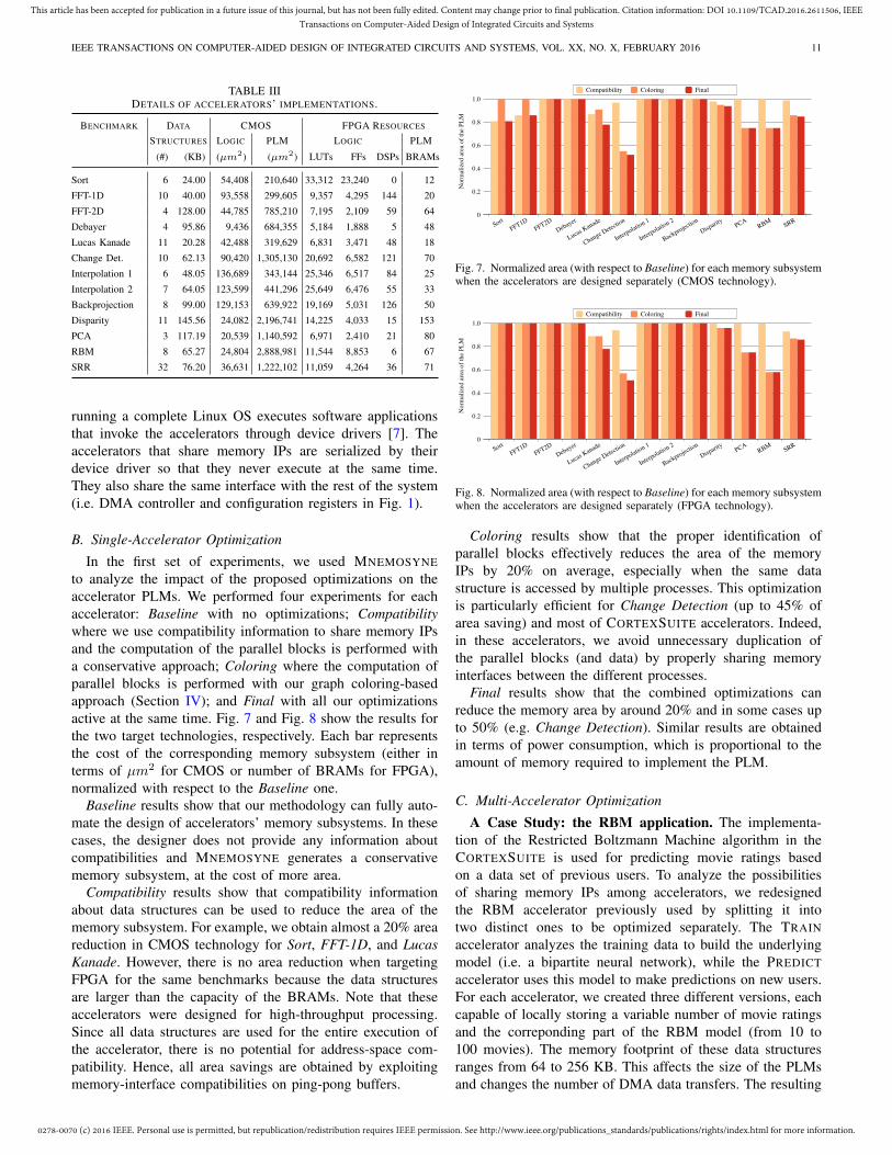
TABLE IIIDETAILS OF ACCELERATORS’ IMPLEMENTATIONS.
BENCHMARK DATA CMOS FPGA RESOURCES
STRUCTURES LOGIC PLM LOGIC PLM
(#) (KB) (µm2) (µm2) LUTs FFs DSPs BRAMs
Sort 6 24.00 54,408 210,640 33,312 23,240 0 12
FFT-1D 10 40.00 93,558 299,605 9,357 4,295 144 20
FFT-2D 4 128.00 44,785 785,210 7,195 2,109 59 64
Debayer 4 95.86 9,436 684,355 5,184 1,888 5 48
Lucas Kanade 11 20.28 42,488 319,629 6,831 3,471 48 18
Change Det. 10 62.13 90,420 1,305,130 20,692 6,582 121 70
Interpolation 1 6 48.05 136,689 343,144 25,346 6,517 84 25
Interpolation 2 7 64.05 123,599 441,296 25,649 6,476 55 33
Backprojection 8 99.00 129,153 639,922 19,169 5,031 126 50
Disparity 11 145.56 24,082 2,196,741 14,225 4,033 15 153
PCA 3 117.19 20,539 1,140,592 6,971 2,410 21 80
RBM 8 65.27 24,804 2,888,981 11,544 8,853 6 67
SRR 32 76.20 36,631 1,222,102 11,059 4,264 36 71
running a complete Linux OS executes software applicationsthat invoke the accelerators through device drivers [7]. Theaccelerators that share memory IPs are serialized by theirdevice driver so that they never execute at the same time.They also share the same interface with the rest of the system(i.e. DMA controller and configuration registers in Fig. 1).
B. Single-Accelerator Optimization
In the first set of experiments, we used MNEMOSYNEto analyze the impact of the proposed optimizations on theaccelerator PLMs. We performed four experiments for eachaccelerator: Baseline with no optimizations; Compatibilitywhere we use compatibility information to share memory IPsand the computation of the parallel blocks is performed witha conservative approach; Coloring where the computation ofparallel blocks is performed with our graph coloring-basedapproach (Section IV); and Final with all our optimizationsactive at the same time. Fig. 7 and Fig. 8 show the results forthe two target technologies, respectively. Each bar representsthe cost of the corresponding memory subsystem (either interms of µm2 for CMOS or number of BRAMs for FPGA),normalized with respect to the Baseline one.
Baseline results show that our methodology can fully auto-mate the design of accelerators’ memory subsystems. In thesecases, the designer does not provide any information aboutcompatibilities and MNEMOSYNE generates a conservativememory subsystem, at the cost of more area.
Compatibility results show that compatibility informationabout data structures can be used to reduce the area of thememory subsystem. For example, we obtain almost a 20% areareduction in CMOS technology for Sort, FFT-1D, and LucasKanade. However, there is no area reduction when targetingFPGA for the same benchmarks because the data structuresare larger than the capacity of the BRAMs. Note that theseaccelerators were designed for high-throughput processing.Since all data structures are used for the entire execution ofthe accelerator, there is no potential for address-space com-patibility. Hence, all area savings are obtained by exploitingmemory-interface compatibilities on ping-pong buffers.
0
0.2
0.4
0.6
0.8
1.0Compatibility Coloring Final
Nor
mal
ized
are
a of
the
PLM
SortFFT1D
FFT2DDebayer
Lucas Kanade
Change Detection
Interpolation 1
Interpolation 2
BackprojectionDisparity PCA
RBM SRR
Fig. 7. Normalized area (with respect to Baseline) for each memory subsystemwhen the accelerators are designed separately (CMOS technology).
0
0.2
0.4
0.6
0.8
1.0Compatibility Coloring Final
Nor
mal
ized
are
a of
the
PLM
SortFFT1D
FFT2DDebayer
Lucas Kanade
Change Detection
Interpolation 1
Interpolation 2
BackprojectionDisparity PCA
RBM SRR
Fig. 8. Normalized area (with respect to Baseline) for each memory subsystemwhen the accelerators are designed separately (FPGA technology).
Coloring results show that the proper identification ofparallel blocks effectively reduces the area of the memoryIPs by 20% on average, especially when the same datastructure is accessed by multiple processes. This optimizationis particularly efficient for Change Detection (up to 45% ofarea saving) and most of CORTEXSUITE accelerators. Indeed,in these accelerators, we avoid unnecessary duplication ofthe parallel blocks (and data) by properly sharing memoryinterfaces between the different processes.
Final results show that the combined optimizations canreduce the memory area by around 20% and in some cases upto 50% (e.g. Change Detection). Similar results are obtainedin terms of power consumption, which is proportional to theamount of memory required to implement the PLM.
C. Multi-Accelerator Optimization
A Case Study: the RBM application. The implementa-tion of the Restricted Boltzmann Machine algorithm in theCORTEXSUITE is used for predicting movie ratings basedon a data set of previous users. To analyze the possibilitiesof sharing memory IPs among accelerators, we redesignedthe RBM accelerator previously used by splitting it intotwo distinct ones to be optimized separately. The TRAINaccelerator analyzes the training data to build the underlyingmodel (i.e. a bipartite neural network), while the PREDICTaccelerator uses this model to make predictions on new users.For each accelerator, we created three different versions, eachcapable of locally storing a variable number of movie ratingsand the correponding part of the RBM model (from 10 to100 movies). The memory footprint of these data structuresranges from 64 to 256 KB. This affects the size of the PLMsand changes the number of DMA data transfers. The resulting
0278-0070 (c) 2016 IEEE. Personal use is permitted, but republication/redistribution requires IEEE permission. See http://www.ieee.org/publications_standards/publications/rights/index.html for more information.
This article has been accepted for publication in a future issue of this journal, but has not been fully edited. Content may change prior to final publication. Citation information: DOI 10.1109/TCAD.2016.2611506, IEEETransactions on Computer-Aided Design of Integrated Circuits and Systems
IEEE TRANSACTIONS ON COMPUTER-AIDED DESIGN OF INTEGRATED CIRCUITS AND SYSTEMS, VOL. XX, NO. X, FEBRUARY 2016 12
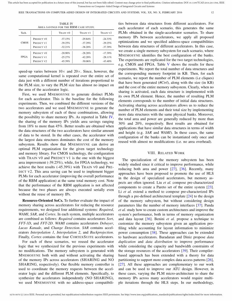
TABLE IVAREA SAVINGS FOR THE RBM CASE STUDY.
Tech. TRAIN V0 TRAIN V1 TRAIN V2
CMOSPREDICT V0 -37.15% -29.84% -24.33%
PREDICT V1 -39.25% -37.29% -29.25%
PREDICT V2 -32.21% -38.20% -37.39%
FPGAPREDICT V0 -20.90% -28.28% -17.39%
PREDICT V1 -25.27% -42.28% -28.11%
PREDICT V2 -45.39% -30.06% -43.40%
speed-up varies between 10× and 20×. Since, however, thesame computational kernel is repeated over the entire set ofdata just with a different number of iterations proportional tothe PLM size, to vary the PLM size has almost no impact onthe area of the accelerator logic.
First, we used MNEMOSYNE to generate distinct PLMsfor each accelerator. This is the baseline for the followingexperiments. Then, we combined the different versions of thetwo accelerators and we used MNEMOSYNE to generate thememory subsystem of each of these combinations, allowingthe possibility to share memory IPs. As reported in Table IV,the sharing of the memory IPs yields area savings rangingfrom 18% to more than 45%. Better results are obtained whenthe data structures of the two accelerators have similar amountof data to be stored. In the other cases, the accelerator withthe largest data structures dominates the cost of the memorysubsystem. Results show that MNEMOSYNE can derive anoptimal PLM organization for the given target technologyand memory library. For CMOS technology, the configurationwith TRAIN V0 and PREDICT V1 is the one with the biggestarea improvement (-39.25%), while, for FPGA technology, weachieve the best results (-45.39%) with TRAIN V0 and PRE-DICT V2. This area saving can be used to implement biggerPLMs for each accelerator (improving the overall performanceof the RBM application) at the same total memory cost. Notethat the performance of the RBM application is not affectedbecause the two phases are always executed serially evenwithout the reuse of memory IPs.
Resource-Oriented SoCs. To further evaluate the impact ofmemory sharing across accelerators for reducing the resourcerequirements, we designed four additional systems: Required,WAMI, SAR, and Cortex. In each system, multiple acceleratorsare combined as follows: Required contains accelerators Sort,FFT-1D, and FFT-2D. WAMI contains accelerators Debayer,Lucas Kanade, and Change Detection. SAR contains accel-erators Interpolation 1, Interpolation 2, and Backprojection.Finally, Cortex contains the four CORTEXSUITE accelerators.
For each of these scenarios, we reused the acceleratorlogic that we synthesized for the previous experiments withno modifications. The memory subsystem is generated withMNEMOSYNE both with and without activating the sharingof the memory IPs across accelerators (SHARING and NOSHARING, respectively). Our flexible memory controller isused to coordinate the memory requests between the accel-erator logic and the different PLM elements. Specifically, tosynthesize the accelerators independently (NO SHARING),we used MNEMOSYNE with no address-space compatibili-
ties between data structures from different accelerators. Foreach accelerator of each scenario, this generates the samePLMs obtained in the single-accelerator scenarios. To sharememory IPs between accelerators, we apply all proposedoptimizations and we specified address-space compatibilitiesbetween data structures of different accelerators. In this case,we create a single memory subsystem for each scenario, whereMNEMOSYNE identifies the best configuration of the banks.The experiments are replicated for the two target technologies,e.g. CMOS and FPGA. Table V shows the results for theseexperiments. We report the total number of data structures andthe corresponding memory footprint in KB. Then, for eachscenario, we report the number of PLM elements (i.e cliques)that have been generated (#Ctrl), along with the size (in KB)and the cost of the entire memory subsystem. Clearly, when nosharing is activated, each data structure is implemented withits own PLM element. Hence, the number of resulting PLMelements corresponds to the number of initial data structures.Activating sharing across accelerators allows us to reduce thenumber of PLM elements and their total size by implementingmore data structures with the same physical banks. Moreover,the total area and power are generally reduced by more than30% and 20%, respectively. Best results are obtained forapplications that have similar data structures in terms of widthand height (e.g. SAR and WAMI). In these cases, the sameconfiguration of the banks can be instantiated only once andreused with almost no modifications (i.e. no area overhead).
VIII. RELATED WORK
The specialization of the memory subsystem has beenwidely studied since it critical to improve performance, whilereducing both area and power [27], [36]. Recently, manyapproaches have been proposed to promote the use of HLSin the design of specialized accelerators, but memory as-pects are often ignored. Liu et al. compose pre-characterizedcomponents to create a Pareto set of the entire system [23].Li et al. extend a method to compose pre-characterized IPsthrough a pre-defined architectural template [24] to the designof the memory subsystem, but without considering designparameters like the number of memory interfaces [37]. Pandaet al. study how to create custom architectures and improve thesystem’s performance, both in terms of memory organizationand data layout [36]. Benini et al. propose a technique tocustomize the memory subsystem given an application pro-filing while accounting for layout information to minimizepower consumption [38]. These approaches can be extendedto hardware accelerators. Baradaran and Diniz propose dataduplication and data distribution to improve performancewhile considering the capacity and bandwidth constraints ofthe storage resources of the accelerators [39]. Their compiler-based approach has been extended with a theory for datapartitioning to support more complex data access patterns [26],[27]. All these approaches are complementary to our workand can be used to improve our ATU design. However, inthese cases, varying the PLM micro-architecture to share thememory IPs across many accelerators would require multi-ple iterations through the HLS steps. In our methodology,
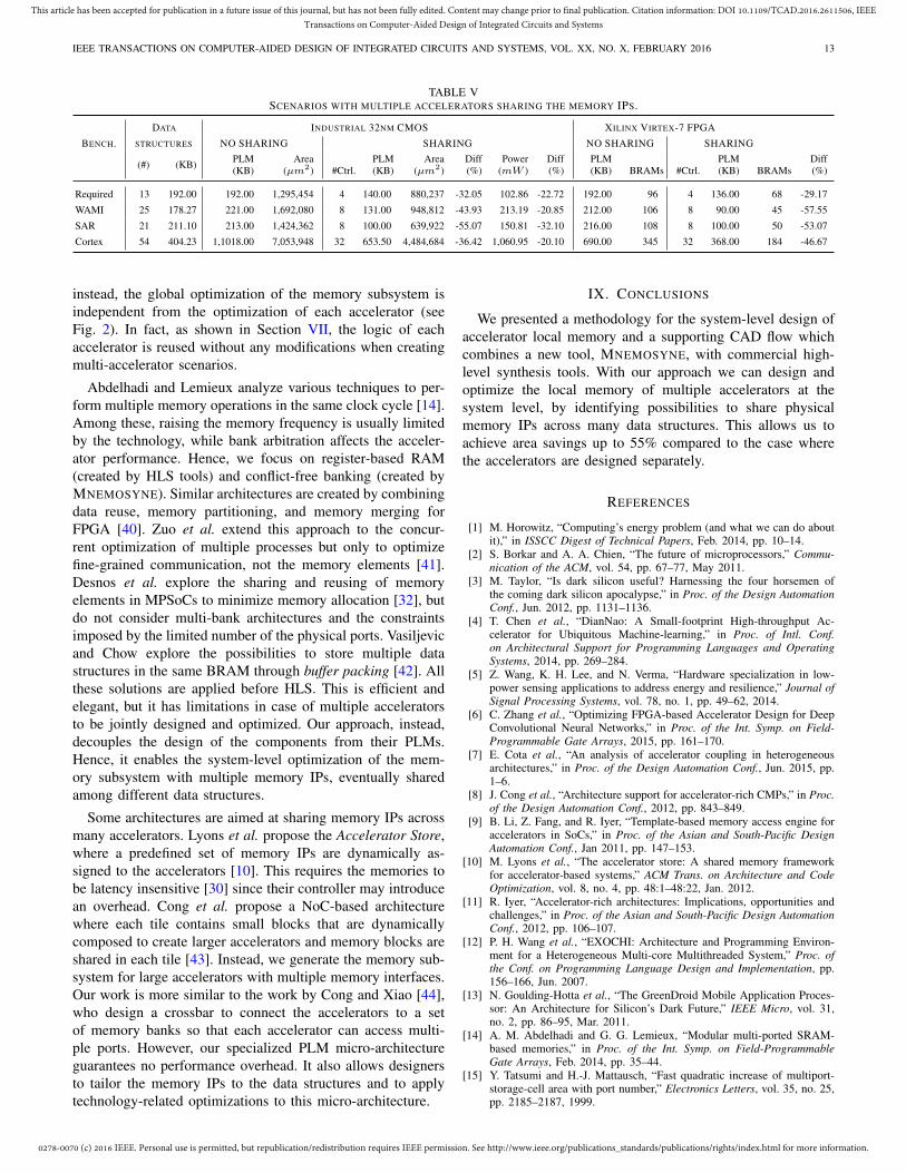
0278-0070 (c) 2016 IEEE. Personal use is permitted, but republication/redistribution requires IEEE permission. See http://www.ieee.org/publications_standards/publications/rights/index.html for more information.
This article has been accepted for publication in a future issue of this journal, but has not been fully edited. Content may change prior to final publication. Citation information: DOI 10.1109/TCAD.2016.2611506, IEEETransactions on Computer-Aided Design of Integrated Circuits and Systems
IEEE TRANSACTIONS ON COMPUTER-AIDED DESIGN OF INTEGRATED CIRCUITS AND SYSTEMS, VOL. XX, NO. X, FEBRUARY 2016 13
TABLE VSCENARIOS WITH MULTIPLE ACCELERATORS SHARING THE MEMORY IPS.
DATA INDUSTRIAL 32NM CMOS XILINX VIRTEX-7 FPGA
BENCH. STRUCTURES NO SHARING SHARING NO SHARING SHARING
(#) (KB) PLM(KB)
Area(µm2) #Ctrl.
PLM(KB)
Area(µm2)
Diff(%)
Power(mW )
Diff(%)
PLM(KB) BRAMs #Ctrl.
PLM(KB) BRAMs
Diff(%)
Required 13 192.00 192.00 1,295,454 4 140.00 880,237 -32.05 102.86 -22.72 192.00 96 4 136.00 68 -29.17
WAMI 25 178.27 221.00 1,692,080 8 131.00 948,812 -43.93 213.19 -20.85 212.00 106 8 90.00 45 -57.55
SAR 21 211.10 213.00 1,424,362 8 100.00 639,922 -55.07 150.81 -32.10 216.00 108 8 100.00 50 -53.07
Cortex 54 404.23 1,1018.00 7,053,948 32 653.50 4,484,684 -36.42 1,060.95 -20.10 690.00 345 32 368.00 184 -46.67
instead, the global optimization of the memory subsystem isindependent from the optimization of each accelerator (seeFig. 2). In fact, as shown in Section VII, the logic of eachaccelerator is reused without any modifications when creatingmulti-accelerator scenarios.
Abdelhadi and Lemieux analyze various techniques to per-form multiple memory operations in the same clock cycle [14].Among these, raising the memory frequency is usually limitedby the technology, while bank arbitration affects the acceler-ator performance. Hence, we focus on register-based RAM(created by HLS tools) and conflict-free banking (created byMNEMOSYNE). Similar architectures are created by combiningdata reuse, memory partitioning, and memory merging forFPGA [40]. Zuo et al. extend this approach to the concur-rent optimization of multiple processes but only to optimizefine-grained communication, not the memory elements [41].Desnos et al. explore the sharing and reusing of memoryelements in MPSoCs to minimize memory allocation [32], butdo not consider multi-bank architectures and the constraintsimposed by the limited number of the physical ports. Vasiljevicand Chow explore the possibilities to store multiple datastructures in the same BRAM through buffer packing [42]. Allthese solutions are applied before HLS. This is efficient andelegant, but it has limitations in case of multiple acceleratorsto be jointly designed and optimized. Our approach, instead,decouples the design of the components from their PLMs.Hence, it enables the system-level optimization of the mem-ory subsystem with multiple memory IPs, eventually sharedamong different data structures.
Some architectures are aimed at sharing memory IPs acrossmany accelerators. Lyons et al. propose the Accelerator Store,where a predefined set of memory IPs are dynamically as-signed to the accelerators [10]. This requires the memories tobe latency insensitive [30] since their controller may introducean overhead. Cong et al. propose a NoC-based architecturewhere each tile contains small blocks that are dynamicallycomposed to create larger accelerators and memory blocks areshared in each tile [43]. Instead, we generate the memory sub-system for large accelerators with multiple memory interfaces.Our work is more similar to the work by Cong and Xiao [44],who design a crossbar to connect the accelerators to a setof memory banks so that each accelerator can access multi-ple ports. However, our specialized PLM micro-architectureguarantees no performance overhead. It also allows designersto tailor the memory IPs to the data structures and to applytechnology-related optimizations to this micro-architecture.
IX. CONCLUSIONS
We presented a methodology for the system-level design ofaccelerator local memory and a supporting CAD flow whichcombines a new tool, MNEMOSYNE, with commercial high-level synthesis tools. With our approach we can design andoptimize the local memory of multiple accelerators at thesystem level, by identifying possibilities to share physicalmemory IPs across many data structures. This allows us toachieve area savings up to 55% compared to the case wherethe accelerators are designed separately.
REFERENCES
[1] M. Horowitz, “Computing’s energy problem (and what we can do aboutit),” in ISSCC Digest of Technical Papers, Feb. 2014, pp. 10–14.
[2] S. Borkar and A. A. Chien, “The future of microprocessors,” Commu-nication of the ACM, vol. 54, pp. 67–77, May 2011.
[3] M. Taylor, “Is dark silicon useful? Harnessing the four horsemen ofthe coming dark silicon apocalypse,” in Proc. of the Design AutomationConf., Jun. 2012, pp. 1131–1136.
[4] T. Chen et al., “DianNao: A Small-footprint High-throughput Ac-celerator for Ubiquitous Machine-learning,” in Proc. of Intl. Conf.on Architectural Support for Programming Languages and OperatingSystems, 2014, pp. 269–284.
[5] Z. Wang, K. H. Lee, and N. Verma, “Hardware specialization in low-power sensing applications to address energy and resilience,” Journal ofSignal Processing Systems, vol. 78, no. 1, pp. 49–62, 2014.
[6] C. Zhang et al., “Optimizing FPGA-based Accelerator Design for DeepConvolutional Neural Networks,” in Proc. of the Int. Symp. on Field-Programmable Gate Arrays, 2015, pp. 161–170.
[7] E. Cota et al., “An analysis of accelerator coupling in heterogeneousarchitectures,” in Proc. of the Design Automation Conf., Jun. 2015, pp.1–6.
[8] J. Cong et al., “Architecture support for accelerator-rich CMPs,” in Proc.of the Design Automation Conf., 2012, pp. 843–849.
[9] B. Li, Z. Fang, and R. Iyer, “Template-based memory access engine foraccelerators in SoCs,” in Proc. of the Asian and South-Pacific DesignAutomation Conf., Jan 2011, pp. 147–153.
[10] M. Lyons et al., “The accelerator store: A shared memory frameworkfor accelerator-based systems,” ACM Trans. on Architecture and CodeOptimization, vol. 8, no. 4, pp. 48:1–48:22, Jan. 2012.
[11] R. Iyer, “Accelerator-rich architectures: Implications, opportunities andchallenges,” in Proc. of the Asian and South-Pacific Design AutomationConf., 2012, pp. 106–107.
[12] P. H. Wang et al., “EXOCHI: Architecture and Programming Environ-ment for a Heterogeneous Multi-core Multithreaded System,” Proc. ofthe Conf. on Programming Language Design and Implementation, pp.156–166, Jun. 2007.
[13] N. Goulding-Hotta et al., “The GreenDroid Mobile Application Proces-sor: An Architecture for Silicon’s Dark Future,” IEEE Micro, vol. 31,no. 2, pp. 86–95, Mar. 2011.
[14] A. M. Abdelhadi and G. G. Lemieux, “Modular multi-ported SRAM-based memories,” in Proc. of the Int. Symp. on Field-ProgrammableGate Arrays, Feb. 2014, pp. 35–44.
[15] Y. Tatsumi and H.-J. Mattausch, “Fast quadratic increase of multiport-storage-cell area with port number,” Electronics Letters, vol. 35, no. 25,pp. 2185–2187, 1999.
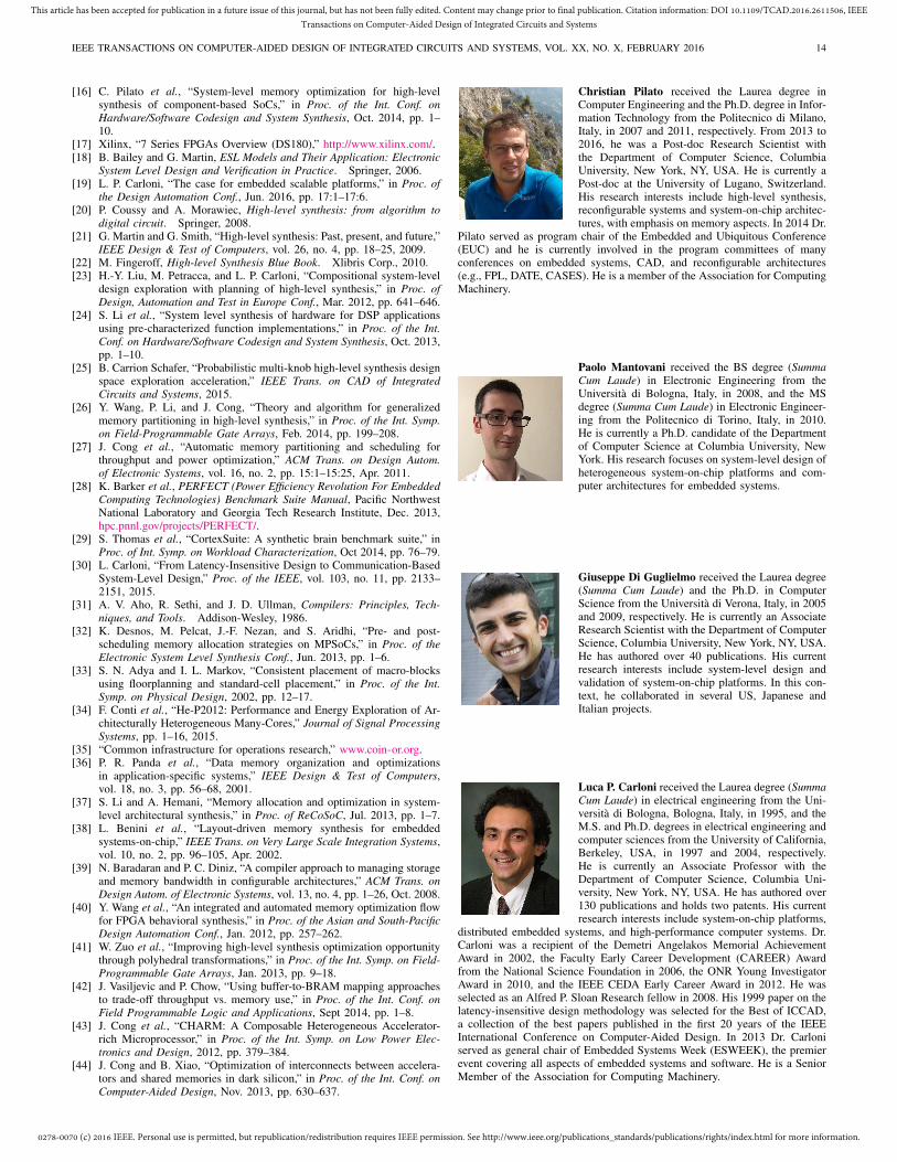
0278-0070 (c) 2016 IEEE. Personal use is permitted, but republication/redistribution requires IEEE permission. See http://www.ieee.org/publications_standards/publications/rights/index.html for more information.
This article has been accepted for publication in a future issue of this journal, but has not been fully edited. Content may change prior to final publication. Citation information: DOI 10.1109/TCAD.2016.2611506, IEEETransactions on Computer-Aided Design of Integrated Circuits and Systems
IEEE TRANSACTIONS ON COMPUTER-AIDED DESIGN OF INTEGRATED CIRCUITS AND SYSTEMS, VOL. XX, NO. X, FEBRUARY 2016 14
[16] C. Pilato et al., “System-level memory optimization for high-levelsynthesis of component-based SoCs,” in Proc. of the Int. Conf. onHardware/Software Codesign and System Synthesis, Oct. 2014, pp. 1–10.
[17] Xilinx, “7 Series FPGAs Overview (DS180),” http://www.xilinx.com/.[18] B. Bailey and G. Martin, ESL Models and Their Application: Electronic
System Level Design and Verification in Practice. Springer, 2006.[19] L. P. Carloni, “The case for embedded scalable platforms,” in Proc. of
the Design Automation Conf., Jun. 2016, pp. 17:1–17:6.[20] P. Coussy and A. Morawiec, High-level synthesis: from algorithm to
digital circuit. Springer, 2008.[21] G. Martin and G. Smith, “High-level synthesis: Past, present, and future,”
IEEE Design & Test of Computers, vol. 26, no. 4, pp. 18–25, 2009.[22] M. Fingeroff, High-level Synthesis Blue Book. Xlibris Corp., 2010.[23] H.-Y. Liu, M. Petracca, and L. P. Carloni, “Compositional system-level
design exploration with planning of high-level synthesis,” in Proc. ofDesign, Automation and Test in Europe Conf., Mar. 2012, pp. 641–646.
[24] S. Li et al., “System level synthesis of hardware for DSP applicationsusing pre-characterized function implementations,” in Proc. of the Int.Conf. on Hardware/Software Codesign and System Synthesis, Oct. 2013,pp. 1–10.
[25] B. Carrion Schafer, “Probabilistic multi-knob high-level synthesis designspace exploration acceleration,” IEEE Trans. on CAD of IntegratedCircuits and Systems, 2015.
[26] Y. Wang, P. Li, and J. Cong, “Theory and algorithm for generalizedmemory partitioning in high-level synthesis,” in Proc. of the Int. Symp.on Field-Programmable Gate Arrays, Feb. 2014, pp. 199–208.
[27] J. Cong et al., “Automatic memory partitioning and scheduling forthroughput and power optimization,” ACM Trans. on Design Autom.of Electronic Systems, vol. 16, no. 2, pp. 15:1–15:25, Apr. 2011.
[28] K. Barker et al., PERFECT (Power Efficiency Revolution For EmbeddedComputing Technologies) Benchmark Suite Manual, Pacific NorthwestNational Laboratory and Georgia Tech Research Institute, Dec. 2013,hpc.pnnl.gov/projects/PERFECT/.
[29] S. Thomas et al., “CortexSuite: A synthetic brain benchmark suite,” inProc. of Int. Symp. on Workload Characterization, Oct 2014, pp. 76–79.
[30] L. Carloni, “From Latency-Insensitive Design to Communication-BasedSystem-Level Design,” Proc. of the IEEE, vol. 103, no. 11, pp. 2133–2151, 2015.
[31] A. V. Aho, R. Sethi, and J. D. Ullman, Compilers: Principles, Tech-niques, and Tools. Addison-Wesley, 1986.
[32] K. Desnos, M. Pelcat, J.-F. Nezan, and S. Aridhi, “Pre- and post-scheduling memory allocation strategies on MPSoCs,” in Proc. of theElectronic System Level Synthesis Conf., Jun. 2013, pp. 1–6.
[33] S. N. Adya and I. L. Markov, “Consistent placement of macro-blocksusing floorplanning and standard-cell placement,” in Proc. of the Int.Symp. on Physical Design, 2002, pp. 12–17.
[34] F. Conti et al., “He-P2012: Performance and Energy Exploration of Ar-chitecturally Heterogeneous Many-Cores,” Journal of Signal ProcessingSystems, pp. 1–16, 2015.
[35] “Common infrastructure for operations research,” www.coin-or.org.[36] P. R. Panda et al., “Data memory organization and optimizations
in application-specific systems,” IEEE Design & Test of Computers,vol. 18, no. 3, pp. 56–68, 2001.
[37] S. Li and A. Hemani, “Memory allocation and optimization in system-level architectural synthesis,” in Proc. of ReCoSoC, Jul. 2013, pp. 1–7.
[38] L. Benini et al., “Layout-driven memory synthesis for embeddedsystems-on-chip,” IEEE Trans. on Very Large Scale Integration Systems,vol. 10, no. 2, pp. 96–105, Apr. 2002.
[39] N. Baradaran and P. C. Diniz, “A compiler approach to managing storageand memory bandwidth in configurable architectures,” ACM Trans. onDesign Autom. of Electronic Systems, vol. 13, no. 4, pp. 1–26, Oct. 2008.
[40] Y. Wang et al., “An integrated and automated memory optimization flowfor FPGA behavioral synthesis,” in Proc. of the Asian and South-PacificDesign Automation Conf., Jan. 2012, pp. 257–262.
[41] W. Zuo et al., “Improving high-level synthesis optimization opportunitythrough polyhedral transformations,” in Proc. of the Int. Symp. on Field-Programmable Gate Arrays, Jan. 2013, pp. 9–18.
[42] J. Vasiljevic and P. Chow, “Using buffer-to-BRAM mapping approachesto trade-off throughput vs. memory use,” in Proc. of the Int. Conf. onField Programmable Logic and Applications, Sept 2014, pp. 1–8.
[43] J. Cong et al., “CHARM: A Composable Heterogeneous Accelerator-rich Microprocessor,” in Proc. of the Int. Symp. on Low Power Elec-tronics and Design, 2012, pp. 379–384.
[44] J. Cong and B. Xiao, “Optimization of interconnects between accelera-tors and shared memories in dark silicon,” in Proc. of the Int. Conf. onComputer-Aided Design, Nov. 2013, pp. 630–637.
Christian Pilato received the Laurea degree inComputer Engineering and the Ph.D. degree in Infor-mation Technology from the Politecnico di Milano,Italy, in 2007 and 2011, respectively. From 2013 to2016, he was a Post-doc Research Scientist withthe Department of Computer Science, ColumbiaUniversity, New York, NY, USA. He is currently aPost-doc at the University of Lugano, Switzerland.His research interests include high-level synthesis,reconfigurable systems and system-on-chip architec-tures, with emphasis on memory aspects. In 2014 Dr.
Pilato served as program chair of the Embedded and Ubiquitous Conference(EUC) and he is currently involved in the program committees of manyconferences on embedded systems, CAD, and reconfigurable architectures(e.g., FPL, DATE, CASES). He is a member of the Association for ComputingMachinery.
Paolo Mantovani received the BS degree (SummaCum Laude) in Electronic Engineering from theUniversita di Bologna, Italy, in 2008, and the MSdegree (Summa Cum Laude) in Electronic Engineer-ing from the Politecnico di Torino, Italy, in 2010.He is currently a Ph.D. candidate of the Departmentof Computer Science at Columbia University, NewYork. His research focuses on system-level design ofheterogeneous system-on-chip platforms and com-puter architectures for embedded systems.
Giuseppe Di Guglielmo received the Laurea degree(Summa Cum Laude) and the Ph.D. in ComputerScience from the Universita di Verona, Italy, in 2005and 2009, respectively. He is currently an AssociateResearch Scientist with the Department of ComputerScience, Columbia University, New York, NY, USA.He has authored over 40 publications. His currentresearch interests include system-level design andvalidation of system-on-chip platforms. In this con-text, he collaborated in several US, Japanese andItalian projects.
Luca P. Carloni received the Laurea degree (SummaCum Laude) in electrical engineering from the Uni-versita di Bologna, Bologna, Italy, in 1995, and theM.S. and Ph.D. degrees in electrical engineering andcomputer sciences from the University of California,Berkeley, USA, in 1997 and 2004, respectively.He is currently an Associate Professor with theDepartment of Computer Science, Columbia Uni-versity, New York, NY, USA. He has authored over130 publications and holds two patents. His currentresearch interests include system-on-chip platforms,
distributed embedded systems, and high-performance computer systems. Dr.Carloni was a recipient of the Demetri Angelakos Memorial AchievementAward in 2002, the Faculty Early Career Development (CAREER) Awardfrom the National Science Foundation in 2006, the ONR Young InvestigatorAward in 2010, and the IEEE CEDA Early Career Award in 2012. He wasselected as an Alfred P. Sloan Research fellow in 2008. His 1999 paper on thelatency-insensitive design methodology was selected for the Best of ICCAD,a collection of the best papers published in the first 20 years of the IEEEInternational Conference on Computer-Aided Design. In 2013 Dr. Carloniserved as general chair of Embedded Systems Week (ESWEEK), the premierevent covering all aspects of embedded systems and software. He is a SeniorMember of the Association for Computing Machinery.


![524 IEEE TRANSACTIONS ON COMPUTER-AIDED … Object Identifier 10.1109/TCAD.2012.2226032 Fig. 1. Liquid-cooled 3-D IC with interlayer microchannels [6]](https://img.pdfslide.us/doc/110x75/5b0bf87b7f8b9a61448dab07/524-ieee-transactions-on-computer-aided-object-identier-101109tcad20122226032.jpg)