Embed Size (px)
Citation preview

1222 IEEE TRANSACTIONS ON COMPUTER-AIDED DESIGN OF INTEGRATED CIRCUITS AND SYSTEMS, VOL. 31, NO. 8, AUGUST 2012
Variation-Aware Clock Network DesignMethodology for Ultralow Voltage (ULV) Circuits
Xin Zhao, Student Member, IEEE, Jeremy R. Tolbert, Student Member, IEEE, Saibal Mukhopadhyay, Member, IEEE,and Sung Kyu Lim, Senior Member, IEEE
Abstract—This paper presents a design methodology for robustand low-energy clock networks for ultralow voltage (ULV)circuits. We show that both clock slew and skew play importantroles in achieving high maximum operating frequency (Fmax) andlow clock energy in ULV circuits. In addition, clock networksin ULV circuits are highly sensitive to process variations. Wepropose a variation-aware methodology that controls both clockskew and slew to maximize Fmax and minimize clock power.In addition, we implement dynamic programming (DP)-basedULV clock routing and buffering methods (deferred mergingand embedding) for deterministic and statistical conditions.Experimental results show that our clock network design methodachieves lower energy (more than 20% savings) at comparableor even higher Fmax compared with the existing methods.
Index Terms—Clock network design, ultralow voltage, varia-tion aware.
I. Introduction
ULTRALOW VOLTAGE (ULV) circuits, where the sup-ply voltage is around or even below the threshold
voltage of transistors, have emerged as an attractive optionfor ultralow-power digital computing. Many ultralow-powerbattery-operated applications with a stringent energy budgetcan benefit from operating in ULV, such as biological moni-toring systems, radio-frequency identification devices, wirelesssensor networks, and others. Although speed is not the primarygoal, high-frequency operation has been demonstrated in therange of tens to hundreds of megahertz [1] with ULV circuits.
The clock network is a global interconnect that providesclock signal to flip-flops (FFs) for synchronization. This net-work contributes a significant amount of power consumptionand dedicates the overall system performance. In the ULVdomain, clock slew plays a major role in robustness of theclock network. This is because in ULV, buffer delay and FFtimings (setup, clock-to-q, and hold) are strong functions ofclock slew [2], [3]. In addition, ULV circuits are more sensitive
Manuscript received September 22, 2011; revised January 12, 2012; ac-cepted February 18, 2012. Date of current version July 18, 2012. This workwas supported by the National Science Foundation, under CCF-0917000,the National Science Foundation Graduate Research Fellowship, under GrantDGE-0644493, and the Semiconductor Research Corporation, under Task ID1836.075. This paper was recommended by Associate Editor D. Sylvester.
The authors are with the School of Electrical and ComputerEngineering, Georgia Institute of Technology, Atlanta, GA 30332USA (e-mail: [email protected]; [email protected]; [email protected]; [email protected]).
Color versions of one or more of the figures in this paper are availableonline at http://ieeexplore.ieee.org.
Digital Object Identifier 10.1109/TCAD.2012.2190825
Fig. 1. Vgs–Ids curves of NMOS and PMOS, where the nominal Vt is621 mV and −575 mV (light curves), respectively. Our design method is forULV clock network design. The supply voltage is set to 550 mV and the 1-σ Vt variation is 10 mV. One thousand Monte Carlo simulation results areshown in two groups of dark curves indicating the Vt variation.
to process and environmental variations, especially thresholdvoltage random variability caused by the random dopantfluctuation and process variations [3]–[5]. Fig. 1 shows Vgs–Ids curves of the NMOS and PMOS from 45-nm predictivetechnology model [6], where the nominal value of thresholdvoltage (Vt) is 621 mV and −575 mV (see the light curves),respectively. The supply voltage (Vdd) is set to 550 mV that isaround the Vt. The threshold voltage variation with 1-σ swingof 10 mV are considered in 1000 Monte Carlo SPICE simula-tion. The results are shown in the two groups of dark curvesindicating the Vt variation. In the ULV domain, the devicecurrent depends exponentially on threshold voltage. Hence,threshold voltage variability can cause a significant variation inclock skew and slew, thereby degrading the timing margins. Asa result, the operating frequency is usually reduced to ensurecorrect operation. Therefore, the clock design methodologyfor ULV circuits requires: 1) efficient control on both clockslew and skew; 2) robustness in the presence of variations;3) consideration of frequency target; and 4) low-energy clockoperation.
In this paper, we develop a variation-aware methodology forrobust and low-energy clock network design for ULV circuits.The contributions of this paper are as follows.
1) We present comprehensive studies based on extensiveexperimental results that show the impact of clock
0278-0070/$31.00 c© 2012 IEEE
ZHAO et al.: VARIATION-AWARE CLOCK NETWORK DESIGN METHODOLOGY 1223
skew and clock slew control on power consumption,performance, and variation tolerance in ULV circuits.
2) We develop a variation-aware ULV clock network designmethodology. For clock skew management, we constructthe routing topology and insert buffers to minimize thedelay differences among the clock paths under bothnominal and statistical conditions. We also show how toefficiently control clock slew bound at each sink underboth nominal and statistical conditions.
3) We implement robust and low-energy clock tree synthe-sis algorithms for ULV clock networks, which are basedon dynamic programming and deferred merging andembedding techniques, so called DP+DME algorithm.Our algorithms generate and save multiple solutions toachieve minimum clock energy while satisfying givenupper bounds for clock slew and skew.
4) Experimental results show that our clock design methodefficiently controls the clock skew and slew in both nom-inal and statistical conditions and constructs ULV clocknetworks with low clock energy at a high maximum op-erating frequency. We outperform state-of-the-art ULVclock-routing methods [2], [7] in terms of performanceand energy under both nominal and statistical conditions.
The remainder of this paper is organized as follows.Section II presents the summary of related work and itslimitations. Section III presents comprehensive study on theclock skew and clock slew variability control impact on clockperformance and energy. Section IV formulates the ULV clocksynthesis problem and presents our clock design methodology.Section V presents our DP and DME-based clock synthesisalgorithm for both nominal and statistical conditions. Ex-perimental results and extensive discussions are presentedin Sections VI and VII, respectively, and we conclude inSection VIII.
II. Background
The history on ULV clock network design is very brief.Existing works focus on minimizing either clock slew or clockskew but not both. Tolbert et al. [8] pointed out the importanceof clock slew control for the reliability of subthreshold circuits.They developed a subthreshold buffer model that consideredthe impact of slew on delay. They also discussed reliable clocksystem design [8] that controls clock slew while minimizingthe energy. In addition, it was shown that traditional clocksynthesis methods for superthreshold circuits are not feasible.However, they did not consider the impact of clock skew onperformance and energy. Seok et al. [7] compared buffered andunbuffered H-tree (UnBH) topologies for various technology,circuit sizes, and supply voltages. For UnBH, clock skewcan be well controlled to near zero, but clock slew maybecome worse. To counter the slew effect, a larger driver isrequired, which results in a significant energy penalty. On theother hand, the buffered H-tree (BufH) may have unbalancedloadings at buffers depending on the buffer level, which canalso cause large skew variability. In addition, both of theseworks are primarily circuit-level studies and did not presentany design method for clock network synthesis. As large-scale
ULV circuits are emerging, methodology is becoming essentialfor automated synthesis of robust (low-slew and low-skew) andlow-energy clock network.
DP-based buffer insertion is one of the common methods insuperthreshold circuits for either timing optimization or clockrouting, which can be classified into wirelength-driven, timing-driven, and maximum slew-constraint-driven with power orarea minimization [9]–[14]. The basic flow is as follows.The multiple feasible buffering solutions with certain costsare stored and propagated, and a global optimal solution isdetermined later. Most of the existing work fix slew violationsby upper bounding the buffer loading. However, this is notsufficient for ULV clock synthesis. Since buffer delay heavilydepends on the input slew, bounding slew in a certain rangedoes not guarantee well management on delay, nor the re-sulting clock skew. Moreover, buffer insertion still takes themerits of repairing the slew, but at the same time leads tomore randomness. Extra cares should be paid on both slewand skew variability control in ULV clock network design.
III. Motivation
A. Clock Slew and Skew Impact on Timing of ULV Circuits
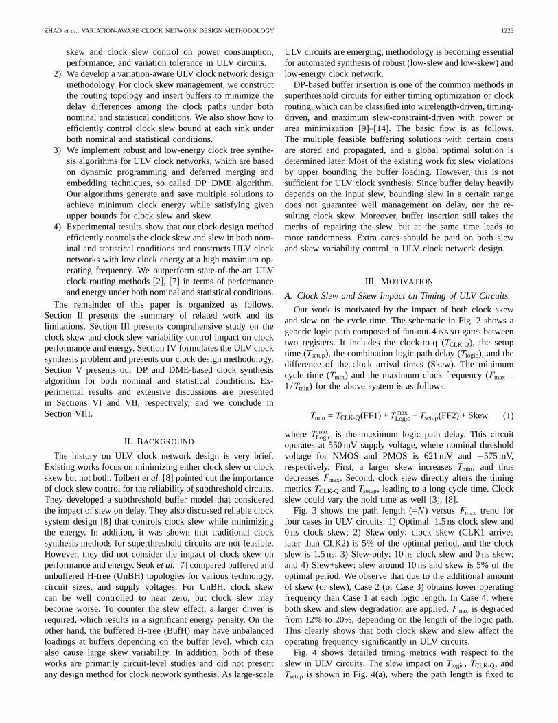
Our work is motivated by the impact of both clock skewand slew on the cycle time. The schematic in Fig. 2 shows ageneric logic path composed of fan-out-4 NAND gates betweentwo registers. It includes the clock-to-q (TCLK-Q), the setuptime (Tsetup), the combination logic path delay (Tlogic), and thedifference of the clock arrival times (Skew). The minimumcycle time (Tmin) and the maximum clock frequency (Fmax =1/Tmin) for the above system is as follows:
Tmin = TCLK-Q(FF1) + T maxLogic + Tsetup(FF2) + Skew (1)
where T maxLogic is the maximum logic path delay. This circuit
operates at 550 mV supply voltage, where nominal thresholdvoltage for NMOS and PMOS is 621 mV and −575 mV,respectively. First, a larger skew increases Tmin, and thusdecreases Fmax. Second, clock slew directly alters the timingmetrics TCLK-Q and Tsetup, leading to a long cycle time. Clockslew could vary the hold time as well [3], [8].
Fig. 3 shows the path length (=N) versus Fmax trend forfour cases in ULV circuits: 1) Optimal: 1.5 ns clock slew and0 ns clock skew; 2) Skew-only: clock skew (CLK1 arriveslater than CLK2) is 5% of the optimal period, and the clockslew is 1.5 ns; 3) Slew-only: 10 ns clock slew and 0 ns skew;and 4) Slew+skew: slew around 10 ns and skew is 5% of theoptimal period. We observe that due to the additional amountof skew (or slew), Case 2 (or Case 3) obtains lower operatingfrequency than Case 1 at each logic length. In Case 4, whereboth skew and slew degradation are applied, Fmax is degradedfrom 12% to 20%, depending on the length of the logic path.This clearly shows that both clock skew and slew affect theoperating frequency significantly in ULV circuits.
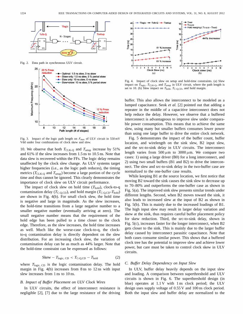
Fig. 4 shows detailed timing metrics with respect to theslew in ULV circuits. The slew impact on Tlogic, TCLK-Q, andTsetup is shown in Fig. 4(a), where the path length is fixed to
1224 IEEE TRANSACTIONS ON COMPUTER-AIDED DESIGN OF INTEGRATED CIRCUITS AND SYSTEMS, VOL. 31, NO. 8, AUGUST 2012
Fig. 2. Data path in synchronous ULV circuit.
Fig. 3. Impact of the logic path length on Fmax of ULV circuit in 550 mVVdd under four combinations of clock skew and slew.
10. We observe that both TCLK-Q and Tsetup increase by 51%and 61% if the slew increases from 1.5 ns to 10.5 ns. Note thatdata slew is recovered within the FFs. The logic delay remainsunaffected by the clock slew change. As ULV systems targethigher frequencies (i.e., as the logic path reduces), the timingmetrics (TCLK-Q and Tsetup) become a large portion of the cycletime and thus cannot be ignored. This clearly demonstrates theimportance of clock slew on ULV circuit performance.
The impact of clock slew on hold time (Thold), clock-to-qcontamination delay (TC-Q,CD), and hold margin (TC-Q,CD-Thold)are shown in Fig. 4(b). For small clock slew, the hold timeis negative and large in magnitude. As the slew increases,the hold-time transitions from a large negative number to asmaller negative number (eventually arriving at zero). Thesmall negative number means that the requirement of thehold edge has been pulled to a time closer to the clockedge. Therefore, as the slew increases, the hold time increasesas well. Much like the worse-case clock-to-q, the clock-to-q contamination delay is directly dependent on the slewdistribution. For an increasing clock slew, the variation ofcontamination delay can be as much as 44% larger. Note thatthe hold-time constraint can be expressed as follows:
Skew − Tlogic, CD < TC-Q,CD − Thold (2)
where Tlogic, CD is the logic contamination delay. The holdmargin in Fig. 4(b) increases from 8 ns to 12 ns with inputslew increases from 1 ns to 10 ns.
B. Impact of Buffer Placement on ULV Clock Wires
In ULV circuits, the effect of interconnect resistance isnegligible [2], [7] due to the large resistance of the driving
Fig. 4. Impact of clock slew on setup and hold-time constraints. (a) Slewimpact on Tlogic, TCLK-Q, and Tsetup in ULV circuit, where the path length isset to 10. (b) Slew impact on Thold, TC-Q,CD, and hold margin.
buffer. This also allows the interconnect to be modeled as alumped capacitance. Seok et al. [2] pointed out that adding arepeater in the middle of a capacitive interconnect does nothelp reduce the delay. However, we observe that a bufferedinterconnect is advantageous to improve slew under compara-ble power consumption. This means that to achieve the sameslew, using many but smaller buffers consumes lower powerthan using one large buffer to drive the entire clock network.
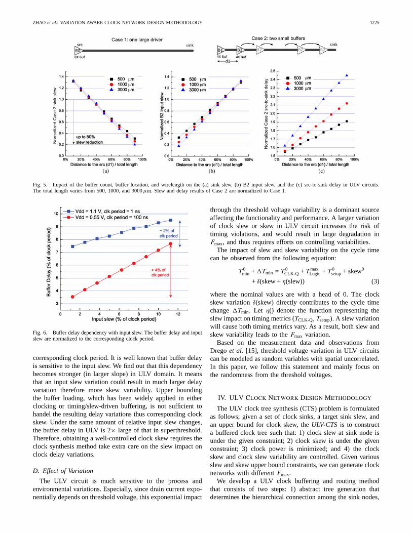
Fig. 5 demonstrates the impact of the buffer count, bufferlocation, and wirelength on the sink slew, B2 input slew,and the src-to-sink delay in ULV circuits. The interconnectlength varies from 500 μm to 3000 μm. We compare twocases: 1) using a large driver (B0) for a long interconnect, and2) using two small buffers (B1 and B2) to drive the intercon-nect. The slew and src-to-sink delay in the two-buffer case arenormalized to the one-buffer case results.
While keeping B1 at the source location, we first notice thatmoving B2 toward the sink causes the sink slew to decrease upto 70–80% and outperforms the one-buffer case as shown inFig. 5(a). The improved sink slew presents similar trends underdifferent lengths. Second, when B2 moves toward the sink, italso leads to increased slew at the input of B2 as shown inFig. 5(b). This is mainly due to the increased loadings of B1.The high input slew may result in larger delay variation andskew at the sink, thus requires careful buffer placement policyfor skew reduction. Third, the src-to-sink delay, shown inFig. 5(c), increases faster for the longer interconnect, when B2gets closer to the sink. This is mainly due to the larger bufferdelay caused by interconnect parasitic capacitance. Note thatboth cases consume similar power. This shows that a bufferedclock tree has the potential to improve slew and achieve lowerpower, but care must be taken to control clock skew in ULVcircuits.
C. Buffer Delay Dependency on Input Slew
In ULV, buffer delay heavily depends on the input slewand loading. A comparison between superthreshold and ULVcircuits is shown in Fig. 6. The superthreshold design (inblue) operates at 1.1 V with 1 ns clock period; the ULVdesign uses supply voltage of 0.55 V and 100 ns clock period.Both the input slew and buffer delay are normalized to the
ZHAO et al.: VARIATION-AWARE CLOCK NETWORK DESIGN METHODOLOGY 1225
Fig. 5. Impact of the buffer count, buffer location, and wirelength on the (a) sink slew, (b) B2 input slew, and the (c) src-to-sink delay in ULV circuits.The total length varies from 500, 1000, and 3000 μm. Slew and delay results of Case 2 are normalized to Case 1.
Fig. 6. Buffer delay dependency with input slew. The buffer delay and inputslew are normalized to the corresponding clock period.
corresponding clock period. It is well known that buffer delayis sensitive to the input slew. We find out that this dependencybecomes stronger (in larger slope) in ULV domain. It meansthat an input slew variation could result in much larger delayvariation therefore more skew variability. Upper boundingthe buffer loading, which has been widely applied in eitherclocking or timing/slew-driven buffering, is not sufficient tohandel the resulting delay variations thus corresponding clockskew. Under the same amount of relative input slew changes,the buffer delay in ULV is 2× large of that in superthreshold.Therefore, obtaining a well-controlled clock skew requires theclock synthesis method take extra care on the slew impact onclock delay variations.
D. Effect of Variation
The ULV circuit is much sensitive to the process andenvironmental variations. Especially, since drain current expo-nentially depends on threshold voltage, this exponential impact
through the threshold voltage variability is a dominant sourceaffecting the functionality and performance. A larger variationof clock slew or skew in ULV circuit increases the risk oftiming violations, and would result in large degradation inFmax, and thus requires efforts on controlling variabilities.
The impact of slew and skew variability on the cycle timecan be observed from the following equation:
T 0min + �Tmin = T 0
CLK-Q + T maxLogic + T 0
setup + skew0
+ δ(skew + η(slew)) (3)
where the nominal values are with a head of 0. The clockskew variation δ(skew) directly contributes to the cycle timechange �Tmin. Let η() denote the function representing theslew impact on timing metrics (TCLK-Q, Tsetup). A slew variationwill cause both timing metrics vary. As a result, both slew andskew variability leads to the Fmax variation.
Based on the measurement data and observations fromDrego et al. [15], threshold voltage variation in ULV circuitscan be modeled as random variables with spatial uncorrelated.In this paper, we follow this statement and mainly focus onthe randomness from the threshold voltages.
IV. ULV Clock Network Design Methodology
The ULV clock tree synthesis (CTS) problem is formulatedas follows; given a set of clock sinks, a target sink slew, andan upper bound for clock skew, the ULV-CTS is to constructa buffered clock tree such that: 1) clock slew at sink node isunder the given constraint; 2) clock skew is under the givenconstraint; 3) clock power is minimized; and 4) the clockskew and clock slew variability are controlled. Given variousslew and skew upper bound constraints, we can generate clocknetworks with different Fmax.
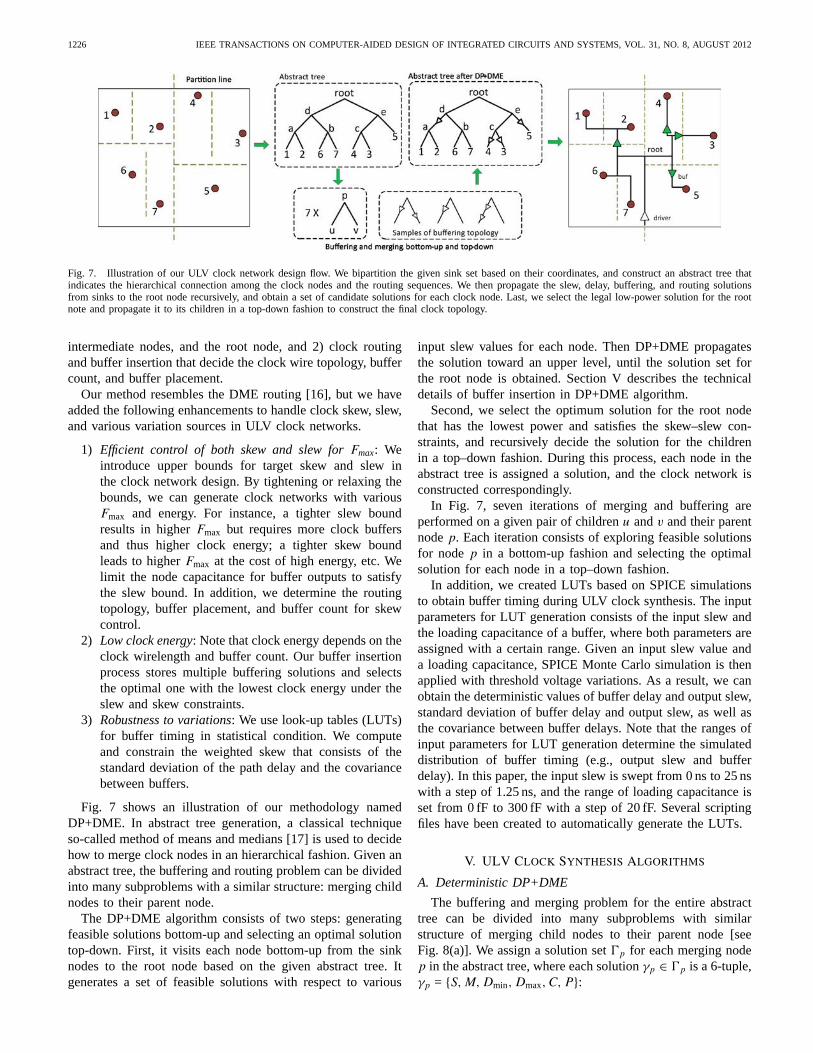
We develop a ULV clock buffering and routing methodthat consists of two steps: 1) abstract tree generation thatdetermines the hierarchical connection among the sink nodes,
1226 IEEE TRANSACTIONS ON COMPUTER-AIDED DESIGN OF INTEGRATED CIRCUITS AND SYSTEMS, VOL. 31, NO. 8, AUGUST 2012
Fig. 7. Illustration of our ULV clock network design flow. We bipartition the given sink set based on their coordinates, and construct an abstract tree thatindicates the hierarchical connection among the clock nodes and the routing sequences. We then propagate the slew, delay, buffering, and routing solutionsfrom sinks to the root node recursively, and obtain a set of candidate solutions for each clock node. Last, we select the legal low-power solution for the rootnote and propagate it to its children in a top-down fashion to construct the final clock topology.
intermediate nodes, and the root node, and 2) clock routingand buffer insertion that decide the clock wire topology, buffercount, and buffer placement.
Our method resembles the DME routing [16], but we haveadded the following enhancements to handle clock skew, slew,and various variation sources in ULV clock networks.
1) Efficient control of both skew and slew for Fmax: Weintroduce upper bounds for target skew and slew inthe clock network design. By tightening or relaxing thebounds, we can generate clock networks with variousFmax and energy. For instance, a tighter slew boundresults in higher Fmax but requires more clock buffersand thus higher clock energy; a tighter skew boundleads to higher Fmax at the cost of high energy, etc. Welimit the node capacitance for buffer outputs to satisfythe slew bound. In addition, we determine the routingtopology, buffer placement, and buffer count for skewcontrol.
2) Low clock energy: Note that clock energy depends on theclock wirelength and buffer count. Our buffer insertionprocess stores multiple buffering solutions and selectsthe optimal one with the lowest clock energy under theslew and skew constraints.
3) Robustness to variations: We use look-up tables (LUTs)for buffer timing in statistical condition. We computeand constrain the weighted skew that consists of thestandard deviation of the path delay and the covariancebetween buffers.
Fig. 7 shows an illustration of our methodology namedDP+DME. In abstract tree generation, a classical techniqueso-called method of means and medians [17] is used to decidehow to merge clock nodes in an hierarchical fashion. Given anabstract tree, the buffering and routing problem can be dividedinto many subproblems with a similar structure: merging childnodes to their parent node.
The DP+DME algorithm consists of two steps: generatingfeasible solutions bottom-up and selecting an optimal solutiontop-down. First, it visits each node bottom-up from the sinknodes to the root node based on the given abstract tree. Itgenerates a set of feasible solutions with respect to various
input slew values for each node. Then DP+DME propagatesthe solution toward an upper level, until the solution set forthe root node is obtained. Section V describes the technicaldetails of buffer insertion in DP+DME algorithm.
Second, we select the optimum solution for the root nodethat has the lowest power and satisfies the skew–slew con-straints, and recursively decide the solution for the childrenin a top–down fashion. During this process, each node in theabstract tree is assigned a solution, and the clock network isconstructed correspondingly.
In Fig. 7, seven iterations of merging and buffering areperformed on a given pair of children u and v and their parentnode p. Each iteration consists of exploring feasible solutionsfor node p in a bottom-up fashion and selecting the optimalsolution for each node in a top–down fashion.
In addition, we created LUTs based on SPICE simulationsto obtain buffer timing during ULV clock synthesis. The inputparameters for LUT generation consists of the input slew andthe loading capacitance of a buffer, where both parameters areassigned with a certain range. Given an input slew value anda loading capacitance, SPICE Monte Carlo simulation is thenapplied with threshold voltage variations. As a result, we canobtain the deterministic values of buffer delay and output slew,standard deviation of buffer delay and output slew, as well asthe covariance between buffer delays. Note that the ranges ofinput parameters for LUT generation determine the simulateddistribution of buffer timing (e.g., output slew and bufferdelay). In this paper, the input slew is swept from 0 ns to 25 nswith a step of 1.25 ns, and the range of loading capacitance isset from 0 fF to 300 fF with a step of 20 fF. Several scriptingfiles have been created to automatically generate the LUTs.
V. ULV Clock Synthesis Algorithms
A. Deterministic DP+DME
The buffering and merging problem for the entire abstracttree can be divided into many subproblems with similarstructure of merging child nodes to their parent node [seeFig. 8(a)]. We assign a solution set �p for each merging nodep in the abstract tree, where each solution γp ∈ �p is a 6-tuple,γp = {S, M, Dmin, Dmax, C, P}:

ZHAO et al.: VARIATION-AWARE CLOCK NETWORK DESIGN METHODOLOGY 1227
Fig. 8. Illustration of determining a solution of node p (γp) by merging nodes u (γu) and v (γv) using deterministic DP+DME. The DP+DME is composedof many subproblems with the similar structure as in (a), where solution γp is determined by first unbuffered or buffered propagating γu (γv) to the solutionγu→p (γv→p) and then applying feasibility check and merging to γp as shown in (b). Given a solution of γu as in (c), the solution γu→p can be obtainedby unbuffered propagation in (d) or buffered propagation in (e). The per-unit-length wire capacitance is set to 0.2 fF/μm, and the buffer loading CBuf() anddelay DBuf() are obtained in the LUT.
1) S is the slew at node p;2) M is the style of merging its child nodes;3) Dmin and Dmax are the minimum and the maximum delay
from node p to its sink nodes;4) C is the loading capacitance at node p;5) P is the cost of the corresponding merging style, which
is the power consumption in this problem.
We use S(γp), Dmin(γp), Dmax(γp), C(γp), and P(γp) torepresent each element in γp.
In bottom-up buffering solution construction, it is impossi-ble to obtain the accurate slew due to its top–down propagationproperty. To accurately acquire the slew and its affecting delay,we enumerate a set of feasible slew value s for each node thats ∈ {s1, s2, . . . , sn}, where si −si-1 = g, s1 and sn are the loweror upper bound, and g is the granularity.
Without loss of generality, considering merging node u andnode v to node p, we first propagate the solution of γu (γv)to node p, and obtain the solution γu→p (γv→p). We thendetermine the solution for node p by merging γu→p and γv→p
to γp with a feasibility check [see Fig. 8(b)]. Depending on,if buffers are inserted along the edge pu (pv), the propagationis classified into buffered or unbuffered-propagation.
In unbuffered-propagation, no buffer is along edge pu. Theelements in solution γu→p are determined as
S(γu→p) = S(γu) (4)
Dmin(γu→p) = Dmin(γu) (5)
Dmax(γu→p) = Dmax(γu) (6)
C(γu→p) = C(γu) + c × lpu (7)
P(γu→p) = P(γu) (8)
where lpu is the length of edge pu and c is the per unit lengthcapacitance of wires. Equations (4)–(8) mean that interconnecthas negligible effect on delay and slew propagation. Note thatif the unbuffered-propagation merging passes the feasibilitycheck from (18) to (21), the lpu = dpu as in (25). Fig. 8(d)shows an example of determining the solution γu→p given thesolution of γu in Fig. 8(c).
In buffered-propagation, a buffer is inserted along edge pu.A set of feasible slew values are assigned at node p. For eachslew value s, solution γu→p for node p are obtained as
S(γu→p) = s (9)
Cb(γu→p) = CBuf(S(γu→p), S(γu)) (10)
Dmin(γu→p) = DBuf(S(γu→p), Cb(γu→p)) + Dmin(γu) (11)
Dmax(γu→p) = DBuf(S(γu→p), Cb(γu→p)) + Dmax(γu) (12)
C(γu→p) = Cin + c × dpb (13)
P(γu→p) = P(γu) + PBuf(S(γu→p), Cb(γu→p)). (14)
We first calculate the buffer loading on edge pu as Cb(γu→p)in (10). The DBuf(), CBuf(), and PBuf() denote LUT op-eration to obtain the buffer delay, loading, and power.For instance, CBuf(S(γu→p), S(γu)) obtains the buffer load-ing given input slew S(γu→p) and output slew S(γu).DBuf(S(γu→p), Cb(γu→p)) denotes the buffer delay given inputslew S(γu→p) and loading Cb(γu→p). Cin is the input capaci-tance of the buffer. Fig. 8(e) shows an example of determiningthe solution γu→p if a buffer is inserted along edge pu. γv→p
follows the similar equations from (4) to (14).When merging γu→p and γv→p into γp
Dmin(γp) = min(Dmin(γu→p), Dmin(γv→p)) (15)
Dmax(γp) = max(Dmax(γu→p), Dmax(γv→p) (16)
C(γp) = C(γu→p) + C(γv→p). (17)
A feasible solution should satisfy all of the following:
S(γu→p) = S(γv→p) = s (18)
Cb(γu→p) ≥ C(γu), if edge pu is buffered (19)
Cb(γv→p) ≥ C(γv), if edge pv is buffered (20)
Skew(γp) = Dmax(γp) − Dmin(γp) ≤ skewBnd. (21)
If the conditions from (18) to (21) are satisfied, we save γp
into �p as a candidate, and the remaining elements in γp areobtained as
S(γp) = s (22)
P(γp) = P(γu→p) + P(γv→p). (23)

1228 IEEE TRANSACTIONS ON COMPUTER-AIDED DESIGN OF INTEGRATED CIRCUITS AND SYSTEMS, VOL. 31, NO. 8, AUGUST 2012
Let L be the minimum merging distance between nodes u andv. In buffered-propagation, let dbu (dbv) denote the distancebetween a buffer to node u (v), which is obtained as
dbu =Cb(γu→p) − C(γu)
c. (24)
For the unbuffered-propagation cases, dbu (dbv) is set to zero.Then the merging distance dpu between nodes p and u (dpv
between p and v) is determined as
dpu = max(L − dbu − dbv
2, 0) + dbu (25)
dpv = max(L − dbu − dbv
2, 0) + dbv. (26)
Correspondingly, the merging style M stores the mergingdistances of dpu, dpv, dbu, and dbv, and a merging segmentfor node p following the classic DME procedure is obtained.
For a sink node p, we choose the feasible slew value s underthe given slew bound slewBnd. For each s ∈ {s1, . . . , sn}, wecreate a solution γp with S(γp) = s, Dmin(γp) = Dmax(γp) =P(γp) = 0, and C(γp) = CFF
in , where CFFin is the input
capacitance of the FF.
B. Pruning the Solutions
Considering that each child node has a number of candidatesolutions, with a combination of the feasible slew for node p,the solution space would be dramatically expanded and losethe efficiency. However, with fewer solutions for node p, itis more difficult to derive a good solution. In addition, theslew granularity g also affects the runtime and final quality.The finer the g, the more candidates for node p, the higherpossibility to consume less power, but the longer runtime. Toguarantee a high quality with reasonable runtime, we definea control parameter K, which is the maximum number ofsolutions for each feasible slew. We increasingly sort thesolutions based on each slew s and keep the first K solutionshaving the smallest power for each feasible slew. We discussthe efficiency of using K and g and their impact on qualityand runtime in the experimental result Section VI-C.
C. Statistical DP+DME
We implement the statistical DP+DME algorithm thatefficiently controls the skew and slew variability duringclocking and buffering procedure. The statistical DP+DMEinvolves many augments on delay and skew randomness.The solution structure is extended as a 7-tuple, γp ={S, M, Dmin, Dmax, C, P, σD}:
1) S is the sample mean of slew at node p;2) Dmin and Dmax are the sample mean of the minimum
and the maximum delay from node p to its sink nodes;3) σD denotes the largest standard deviation of the path
delay from node p to the sinks;4) M is the style of merging its child nodes;5) C is the loading capacitance at node p;6) P is the cost of the corresponding merging style, which
is the power consumption in this problem.
The statistical DP+DME utilizes variation-aware LUTs, whichinclude the sample mean and standard deviation of delay and
slew with respect to the input slew and loading capacitance,as well as the covariance between buffer delays.
Most of the elements in solution γp follow the similarpropagation policy as the deterministic DP+DME method. TheσD(γu→p) is updated as follows.
In the case of buffered-propagation
σ2D(γu→p) = σ2
D(γu) + VBuf(S(γu→p)Cb(γu→p)) + Cov. (27)
We calculate the covariance between buffers along the pathpu and each of the buffers connecting to it. We then add thelargest covariance value (Cov) into the σD(γu→p). The VBuf()denotes the variance of the buffer along path pu with inputslew S(γu→p) and loading Cb(γu→p) obtained from the LUT.
After merging γu→p and γv→p to γp, σD(γp) is obtained asfollows:
σD(γp) = max(σD(γu→p), σD(γv→p)). (28)
The statistical skew depends on not only the differencesamong the average path delays but also the delay variance.We use a weighted sum (SSkew) to represent this dependency
SSkew(γp) = α × (Dmax(γp) − Dmin(γp)) + β × σD(γp) (29)
where weights α=1, β=2 are used to express the worst-caseskew variability, and the feasibility check for the skewBndconstraint (21) is updated as
SSkew(γp) ≤ skewBnd. (30)
For simplicity, the weighted equation (29) is used to controlthe skew variability. Our method is flexible to employ moresophisticated method as [18]. In addition, slew variability canbe directly improved by applying a tighter slew constraint.
VI. Simulation and Discussions
A. Experimental Settings
Our clock design method has been implemented usingC++/STL on Linux. We focus on the 45-nm technology ULVclock network design. The per-unit-length wire resistanceand capacitance are 0.1 /μm and 0.2 fF/μm, respectively.Our clock network uses 6× buffers. The nominal values ofthreshold voltage (Vt) is 621 mV and −575 mV for NMOSand PMOS, respectively. The supply voltage (Vdd) is set to550 mV that is around the Vt and the 1-σ threshold voltageswing is 10 mV.
All experimental results are reported from SPICE simula-tion, including clock skew, slew, and energy per cycle. We useLUT-based buffer modeling during clock network constructionand evaluate the designs using SPICE: 1) we extract the layoutinformation of the FFs; 2) apply our ULV clock synthesismethod to construct a buffered clock tree; and 3) extract aclock netlist for SPICE simulation. In statistical condition, theVt uncertainty is modeled as random variables with spatialuncorrelated [15]. We apply 1000 Monte Carlo simulationsfor each design and report μ+2σ skew and slew like theexisting work [7]. We created five benchmark circuits: three

ZHAO et al.: VARIATION-AWARE CLOCK NETWORK DESIGN METHODOLOGY 1229
TABLE I
Information of Benchmark and Energy Per Cycle (pJ)
Energy per Cycleckt Function #Gates #FFs Area Logic+Wire H-Tree
(μm×μm) w/o clock (% of tot)ckt1 FIR filter 3823 148 331×315 2.1 1.1 (34%)ckt2 Multiplier 3952 320 376×412 4.4 2.5 (36%)ckt3 FIR filter 16 185 499 664×664 6.3 4.1 (39%)ckt4 FIR filter 30 833 619 857×924 13.4 5.5 (29%)ckt5 Quick sort 4828 768 518×546 7.6 4.8 (39%)
Fig. 9. Sample layout of a clock network for a FIR filter with 619 clocksinks and 24 937 μm wirelength.
Fig. 10. Clock waveforms for a FIR filter with 148 FFs at 10 MHz frequency.Clock skew is 1.2 ns, and it distributes from 3.1 ns to 5.3 ns with an averagevalue of 4.7 ns.
finite impulse response (FIR) filters, a multiplier, and a designimplementing quick sort as shown in Table I.
Fig. 9 shows a clock network for our FIR filter, which isseen in front of the logic cells and highlighted FFs. The clocknetwork has 619 clock sinks, a total wirelength of 24 937 μm,and die area of 857 μm×924μm.
Fig. 10 shows the clock waveforms from SPICE for aFIR filter (ckt1) in ULV operation. This superimposes 148waveforms from the FFs. The clock skew is 1.2 ns, which canbe observed by the width of waveforms at 50% Vdd. The clockslew values for all the sinks are from 3.1 ns to 5.3 ns with anaverage of 4.7 ns.
Fig. 11. Fmax versus energy per cycle in nominal condition for ckt1.
B. Impact of Slew and Skew Bounds on Fmax and Energy
Fig. 11 shows the impact of skew and slew upper boundson Fmax and clock energy per cycle for ckt1. We show fourcurves of nominal results: one is for UnBHs and the other threeare generated by our DP+DME clock synthesis technique. TheUnBH takes an advantage of skew minimization. However, itneeds a large driver for entire network to ensure small clockslew at sink nodes. Therefore, we upsize the driver (an inverterchain) to improve the Fmax. As a result, the overall clockenergy of the UnBH increases significantly. In the case ofDP+DME, we present three groups of results, where clocknetworks in each group are designed under the same skewbounds (1 ns, 3 ns, and 10 ns) but different slew bounds (from3 ns to 8 ns).
First, Fig. 11 demonstrates the tradeoff between high Fmax
and low clock energy, i.e., design for a higher Fmax consumesmore clock energy. In each DP+DME curve under the sameskew constraint, a tighter slew bound improves Fmax. Mean-while, the clock energy per cycle increases due to more buffersthat are inserted for tighter slew control. Second, the design of3 ns skew bound consumes lower energy than 1 ns skew bound.This is mainly because the 3 ns skew constraint reserves morefeasible solutions during clock network construction, whichhelps to obtain a low-energy clock network. However, usingrelaxed skew bound of 10 ns cannot hold this benefit, sinceit allows larger clock skew thus requires more buffers fortighter slew to reach a similar Fmax as 1 ns or 3 ns skewbound. Third, compared with the UnBH design targeting atskew minimization only, our method achieves up to 30%energy reduction in the frequency range from 8.0 MHz to8.4 MHz. This is because a buffered clock tree has shorterwirelength and a smaller driver than the UnBH design. Wenote that a higher Fmax target will shorten the energy gapbetween ours and the UnBH. Under the relaxed skew bound,the clock energy increases slower than that of tight skewbound as the slew bound increases. But, the relaxed skewbound results in lower Fmax than other two curves. Thus, wesee that by controlling both the skew and slew bounds, wedesign a low-energy clock network for a given target Fmax
more effectively.

1230 IEEE TRANSACTIONS ON COMPUTER-AIDED DESIGN OF INTEGRATED CIRCUITS AND SYSTEMS, VOL. 31, NO. 8, AUGUST 2012
TABLE II
Deterministic Clock Routing Results Under Various Slew and Skew Bounds Including Wirelength (μm),
Buffer Count, Skew (ns), Slew (ns), and Clock Energy Per Cycle (pJ)
Slew Skew WL #Bufs Skew Min Slew Max Slew Avg. Slew Energy Per CycleBound Bound LUT SPICE LUT SPICE LUT SPICE LUT SPICE SPICE Ratio
0.5 6678 40 0.27 0.38 2.5 2.5 3.0 2.9 2.7 2.6 1.17 1.003 1.0 5268 40 0.81 0.78 1.5 1.5 3.0 2.9 2.5 2.4 1.09 0.93
2.0 5159 39 1.56 1.70 2.0 1.9 3.0 2.9 2.5 2.4 1.08 0.920.5 7761 28 0.50 0.51 3.5 3.5 5.0 4.8 4.1 4.0 1.14 0.97
5 1.0 5864 27 1.00 0.98 3.0 3.0 5.0 4.8 4.0 3.8 1.01 0.862.0 5127 25 1.79 1.92 2.0 2.0 5.0 4.8 3.8 3.7 0.94 0.800.5 6104 16 0.50 0.50 5.5 5.4 6.5 6.3 5.6 5.4 0.91 0.78
7 1.0 5501 16 0.75 0.73 5.0 4.9 6.5 6.3 5.3 5.2 0.87 0.742.0 4968 16 1.26 1.23 4.0 4.0 6.5 6.3 5.1 5.0 0.84 0.72
Both LUT and SPICE simulation results are included in clock timing.
C. Deterministic Clock Routing Results
1) Efficiency of Slew and Skew Control: Table II showsclock synthesis results under various upper bounds for theslew and skew using deterministic DP+DME algorithm. Weshow the wirelength (μm), buffer count, clock skew (ns),slew distribution (min/max/avg) (ns), and clock energy percycle (pJ). First, LUT-based modeling approach is trustworthyto estimate the buffer timing during clock synthesis. Bycomparing the value from LUT and SPICE simulation, thedifferences are within 0.2 ns. Second, for each design, bothclock skew and slew from SPICE simulation are under thegiven upper bounds. This demonstrates the efficiency of ourdeterministic DP+DME algorithm in controlling both clockskew and slew for ULV circuits.
2) Runtime Versus Quality Tradeoff: Fig. 12 shows thecomparisons for normalized clock energy per cycle and run-time using two slew granularity g={0.5 ns, 0.25 ns} and themaximum allowed solution count K for each feasible slewvalue, where K={2, 5, 10, 20}, correspondingly. The resultingclock energy and overall runtime are closely related to thesetwo settings in the DP algorithm. A lower energy clock designcan be obtained by either using finer slew granularity orstoring more intermediate solutions. However, at the sametime, a significant amount of runtime has to be paid to findan optimal solution in DP+DME algorithm. We choose 0.5 nsslew granularity and allow maximum ten solutions for eachfeasible slew in the DP+DME for the consideration of bothlow-energy clock design and reasonable runtime.
D. Statistical Versus Deterministic Methods
Fig. 13 shows the efficiency of our variation-aware method-ology. We compare the deterministic and statistical DP+DMEtechniques in terms of the μ+2σ skew, the worst-case skew,and the clock energy. There are two major differences betweenthese two methods: 1) statistical DP+DME uses variation-aware LUTs, which include the sample mean and standarddeviation of delay and slew with respect to the input slew andloading capacitance, as well as the covariance between bufferdelays, and 2) we employ the statistical skew bound to copewith the control on the variation-caused skew uncertainty. Weobserve that both μ+2σ and the worst-case skew are efficiently
Fig. 12. Impact of the slew granularity g and the maximum number ofsolutions K for each feasible slew value on the energy per cycle and runtime,where g={0.5 ns, 0.25 ns} and K={2, 5, 10, 20}.
Fig. 13. Comparisons between deterministic and statistical DP+DMEtechniques in μ+2σ skew and the worst-case skew.
reduced by using the statistical method with marginal energypenalty.
E. Comparison With Existing Works
For ULV circuit clock tree routing, Tolbert et al. [2] focusedon clock slew minimization only for low power and reliability.Seok et al. [7] compared UnBH and BufH topologies in ULVoperation under different supply voltages, technologies, and
ZHAO et al.: VARIATION-AWARE CLOCK NETWORK DESIGN METHODOLOGY 1231
TABLE III
Comparisons Between LSHS Method [2] and Our DP+DME Algorithm in Nominal and Statistical Conditions
In Nominal Condition In Statistical Condition Reduction %ckt Method WL #B Skew Slew EPC Skew MaxSlew Skew EPC Skew Skew
Max μ σ μ+2σ Worst μ σ Nom. μ+2σ Worstckt1 LSHS 4968 31 16.7 3.8 0.99 17.7 1.8 21.2 23.5 4.9 0.6
Our DP+DME 5725 32 1.9 3.8 1.04 4.5 2.0 8.5 13.7 4.9 0.6 88.7 −5.7 59.7 41.6ckt2 LSHS 10 760 65 14.7 3.9 2.11 16.8 1.6 19.9 23.3 5.2 0.6
Our DP+DME 11 061 66 3.1 3.8 2.13 6.4 1.9 10.2 13.3 5.1 0.6 79.0 −1.1 48.6 43.1ckt3 LSHS 19 497 109 15.2 3.9 3.53 17.8 1.6 20.9 25.2 5.6 0.6
Our DP+DME 20 719 113 3.0 3.8 3.64 7.4 1.7 10.8 16.5 5.5 0.6 80.3 −3.1 48.3 34.7ckt4 LSHS 26 603 127 15.4 3.9 4.43 19.1 2.2 23.6 28.3 5.8 0.6
Our DP+DME 27 794 131 1.7 3.8 4.54 8.5 2.1 12.8 17.1 5.7 0.6 89.1 −2.4 45.8 39.5ckt5 LSHS 21 101 144 15.2 3.9 4.64 18.8 1.8 22.4 31.2 5.8 0.6
Our DP+DME 23 703 151 2.6 3.8 4.86 8.1 1.8 11.7 15.5 5.6 0.6 83.2 −4.8 47.6 50.3
We show the wirelength (μm), skew (ns), slew (ns), and energy per cycle (EPC in pJ).
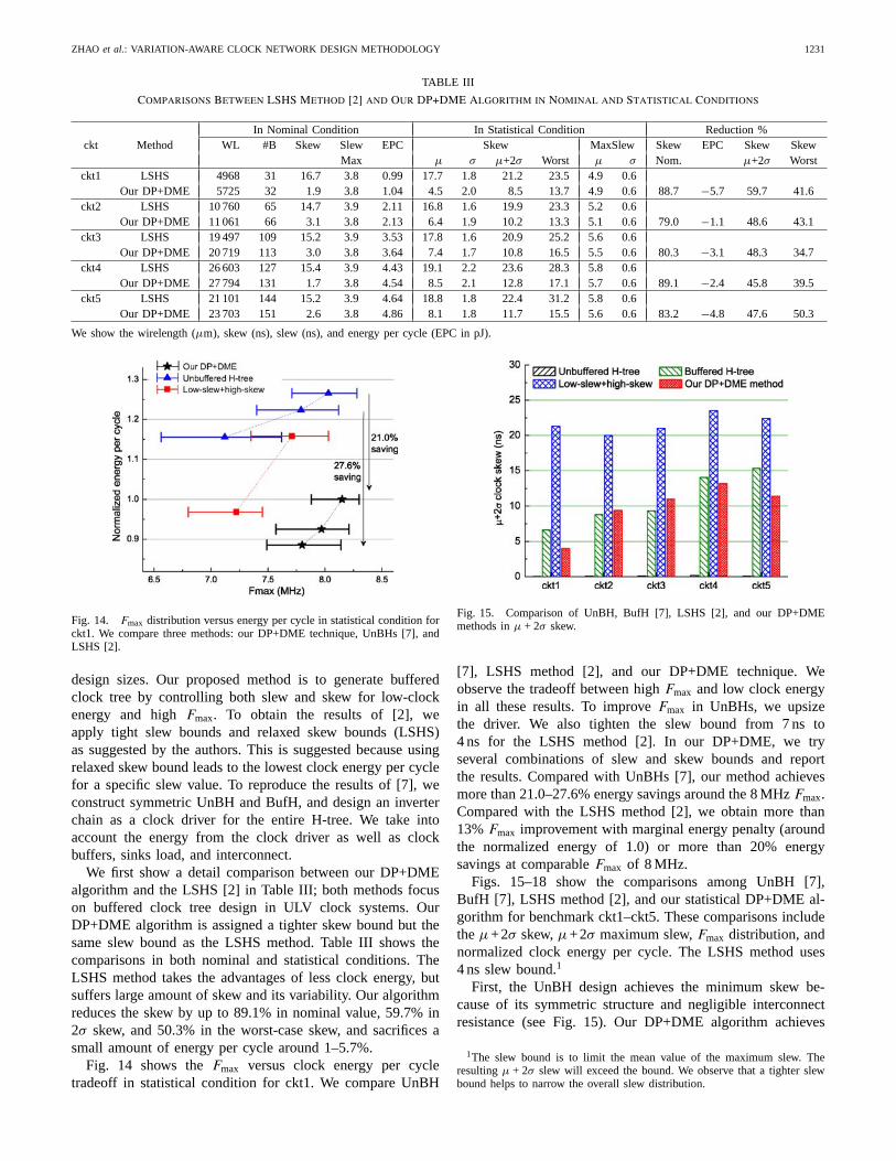
Fig. 14. Fmax distribution versus energy per cycle in statistical condition forckt1. We compare three methods: our DP+DME technique, UnBHs [7], andLSHS [2].
design sizes. Our proposed method is to generate bufferedclock tree by controlling both slew and skew for low-clockenergy and high Fmax. To obtain the results of [2], weapply tight slew bounds and relaxed skew bounds (LSHS)as suggested by the authors. This is suggested because usingrelaxed skew bound leads to the lowest clock energy per cyclefor a specific slew value. To reproduce the results of [7], weconstruct symmetric UnBH and BufH, and design an inverterchain as a clock driver for the entire H-tree. We take intoaccount the energy from the clock driver as well as clockbuffers, sinks load, and interconnect.
We first show a detail comparison between our DP+DMEalgorithm and the LSHS [2] in Table III; both methods focuson buffered clock tree design in ULV clock systems. OurDP+DME algorithm is assigned a tighter skew bound but thesame slew bound as the LSHS method. Table III shows thecomparisons in both nominal and statistical conditions. TheLSHS method takes the advantages of less clock energy, butsuffers large amount of skew and its variability. Our algorithmreduces the skew by up to 89.1% in nominal value, 59.7% in2σ skew, and 50.3% in the worst-case skew, and sacrifices asmall amount of energy per cycle around 1–5.7%.
Fig. 14 shows the Fmax versus clock energy per cycletradeoff in statistical condition for ckt1. We compare UnBH
Fig. 15. Comparison of UnBH, BufH [7], LSHS [2], and our DP+DMEmethods in μ + 2σ skew.
[7], LSHS method [2], and our DP+DME technique. Weobserve the tradeoff between high Fmax and low clock energyin all these results. To improve Fmax in UnBHs, we upsizethe driver. We also tighten the slew bound from 7 ns to4 ns for the LSHS method [2]. In our DP+DME, we tryseveral combinations of slew and skew bounds and reportthe results. Compared with UnBHs [7], our method achievesmore than 21.0–27.6% energy savings around the 8 MHz Fmax.Compared with the LSHS method [2], we obtain more than13% Fmax improvement with marginal energy penalty (aroundthe normalized energy of 1.0) or more than 20% energysavings at comparable Fmax of 8 MHz.
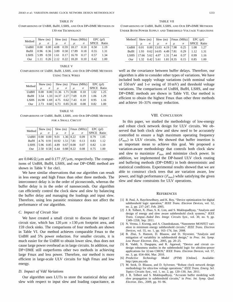
Figs. 15–18 show the comparisons among UnBH [7],BufH [7], LSHS method [2], and our statistical DP+DME al-gorithm for benchmark ckt1–ckt5. These comparisons includethe μ+2σ skew, μ+2σ maximum slew, Fmax distribution, andnormalized clock energy per cycle. The LSHS method uses4 ns slew bound.1
First, the UnBH design achieves the minimum skew be-cause of its symmetric structure and negligible interconnectresistance (see Fig. 15). Our DP+DME algorithm achieves
1The slew bound is to limit the mean value of the maximum slew. Theresulting μ + 2σ slew will exceed the bound. We observe that a tighter slewbound helps to narrow the overall slew distribution.

1232 IEEE TRANSACTIONS ON COMPUTER-AIDED DESIGN OF INTEGRATED CIRCUITS AND SYSTEMS, VOL. 31, NO. 8, AUGUST 2012
Fig. 16. Comparison of UnBH, BufH [7], LSHS [2], and our DP+DMEmethods in μ + 2σ maximum slew.
Fig. 17. Comparison of UnBH, BufH [7], LSHS [2], and our DP+DMEmethods in Fmax distribution.
comparable or even better skew compared with BufH de-sign, whereas the LSHS method results in the largest skewdegradation.
Second, the LSHS method shows the advantage in minimiz-ing the variation-aware slew (see Fig. 16). Both unbufferedand BufHs have high slew. This large slew degradation canbe reduced by upsizing the driver or the internal clock bufferswith inevitable penalty of extreme larger clock energy.
Third, because we efficiently control both clock skew andslew, our method obtains a high Fmax (see Fig. 17) andoutperforms the other three methods in achieving the lowestclock energy (i.e., 10–40% energy savings, see Fig. 18).Fig. 19 shows the variation-aware Fmax distribution of thefour methods for ckt1. Our clock network achieves the highestsample mean Fmax of 8.2 MHz and narrower standard deviationof 0.08 MHz. This is comparable with UnBH result and muchbetter than other two methods.
In addition, the LSHS method achieves lower energy thanUnBHs at the cost of low Fmax. The BufH consumes the high-est energy but in low Fmax, which matches the observations [7].Therefore, we conclude that a simultaneous management ofvariation-aware slew and skew proves to be an efficient wayto obtain a low-energy and robust clock network targeting ata high Fmax in ULV circuits.
Fig. 18. Comparison of UnBH, BufH [7], LSHS [2], and our DP+DMEmethods in normalized energy per cycle.
Fig. 19. Comparison of Fmax distribution among UnBH, BufH, LSHS, andour DP+DME for ckt1.
VII. Extensive Discussions
A. Results of 130-nm Technology
We extend our discussion on 130-nm technology. The com-parisons of UnBH, BufH, low-slew and high-skew (LSHS),and our DP+DME method are shown in Table IV for ckt1. Thethreshold voltage of NMOS and PMOS from 130-nm PTMmodel are 378 mV and −4321 mV, respectively. The supplyvoltage is set to 300 mV with 1-σ threshold voltage swing as10 mV. The per-unit-length wire resistance and capacitance are0.028 /μm and 0.267 fF/μm, respectively. The interconnectparasitic resistance is much lower in 130 nm than in 45-nmtechnology.
We have consistent observations that: 1) our DP+DMEalgorithm achieves comparable Fmax distribution and 19%less power than UnBH; 2) compared with the LSHS and BufHmethods, we obtain both higher Fmax and more than 30%power reduction; and 3) UnBH results in near-zero skew andLSHS method has lowest slew. But our DP+DME methodcontrols both slew and skew variability.
B. Impact of Wire Thickness
In this section, we discuss the impact of wire thickness onULV clock performance. Note that our DP+DME algorithmis able to consider various interconnect parasitics or usingdifferent technology. To reduce the parasitic resistance, weuse thin-global interconnect with 0.8 μm thick, 0.6 μm wide,and 0.4 μm space, which refers to the metal layers [19]. Thecorresponding per-unit-length wire resistance and capacitance
ZHAO et al.: VARIATION-AWARE CLOCK NETWORK DESIGN METHODOLOGY 1233
TABLE IV
Comparisons of UnBH, BufH, LSHS, and Our DP+DME Methods in
130-nm Technology
MethodSkew (ns) Slew (ns) Fmax (MHz) EPC (pJ)μ σ μ σ μ σ SPICE Ratio
UnBH 0.00 0.00 4.08 0.59 18.17 0.10 0.50 1.19BufH 0.96 0.36 3.89 0.58 17.89 0.18 0.55 1.31LSHS 5.99 0.59 1.61 0.17 16.70 0.17 0.57 1.34Our 1.11 0.26 2.12 0.22 18.20 0.10 0.42 1.00
TABLE V
Comparisons of UnBH, BufH, LSHS, and Our DP+DME Methods
Using Thick Wires
MethodSkew (ns) Slew (ns) Fmax (MHz) EPC (pJ)μ σ μ σ μ σ SPICE Ratio
UnBH 0.00 0.00 11.36 1.71 8.08 0.10 1.02 1.25BufH 3.54 1.33 14.37 2.27 7.69 0.19 1.06 1.29LSHS 16.98 1.69 4.75 0.62 7.43 0.10 0.95 1.16Our 2.73 0.60 6.73 0.85 8.18 0.08 0.82 1.00
TABLE VI
Comparisons of UnBH, BufH, LSHS, and Our DP+DME Methods
for a Small Circuit
MethodSkew (ns) Slew (ns) Fmax (MHz) EPC (pJ)μ σ μ σ μ σ SPICE Ratio
UnBH 0.00 0.00 9.01 1.36 8.22 0.09 0.79 1.05BufH 4.76 0.91 10.92 1.51 7.81 0.13 0.83 1.12LSHS 5.96 0.85 4.89 0.67 8.08 0.07 0.82 1.10Our 2.50 0.58 6.44 0.88 8.22 0.08 0.75 1.00
are 0.046 /μm and 0.177 fF/μm, respectively. The compar-isons of UnBH, BufH, LSHS, and our DP+DME method areshown in Table V for ckt1.
We have similar observations that our algorithm can resultin less energy and high Fmax than other three methods. Theinterconnect delay is in the order of picoseconds, whereas thebuffer delay is in the order of nanoseconds. Our algorithmcan efficiently control the clock skew and slew by balancingthe buffer delay and managing the loadings and input slew.Therefore, using less parasitic resistance does not affect theperformance of our algorithm.
C. Impact of Circuit Size
We have created a small circuit to discuss the impact ofcircuit size, which has 120 μm ×130 μm footprint area, and159 clock sinks. The comparisons of four methods are shownin Table VI. Our method achieves comparable Fmax to theUnBH and 5% power reduction. For smaller circuits, it ismuch easier for the UnBH to obtain lower slew, thus does notcause large power overhead as in large circuits. In addition, ourDP+DME still outperforms other two methods in achievinglarge Fmax and less power. Therefore, our method is moreefficient in large-scale ULV circuits for high Fmax and lowenergy.
D. Impact of Vdd Variations
Our algorithm uses LUTs to store the statistical delay andslew with respect to input slew and loading capacitance, as
TABLE VII
Comparisons of UnBH, BufH, LSHS, and Our DP+DME Methods
Under Both Power Supply and Threshold Voltage Variations
Method Skew (ns) Slew (ns) Fmax (MHz) EPC (pJ)μ σ μ σ μ σ SPICE Ratio
UnBH 0.01 0.00 13.03 4.19 7.98 0.25 1.08 1.27BufH 1.93 0.62 14.05 4.49 7.81 0.29 1.12 1.31LSHS 17.66 5.62 4.07 1.31 7.44 0.37 0.99 1.16Our 1.32 0.42 5.61 1.81 8.35 0.15 0.85 1.00
well as the covariance between buffer delays. Therefore, ouralgorithm is able to consider other types of variations. We haveincluded both supply voltage variations (with nominal valueof 550 mV and 1-σ swing of 10 mV) and threshold voltagevariations. The comparisons of UnBH, BufH, LSHS, and ourDP+DME methods are shown in Table VII. Our method isefficient to obtain the highest Fmax than other three methodsand achieve 16–31% energy reduction.
VIII. Conclusion
In this paper, we studied the methodology of low-energyand robust clock network design for ULV circuits. We ob-served that both clock slew and skew need to be accuratelycontrolled to ensure a high maximum operating frequency(Fmax) in ULV circuits. We showed that buffer insertion isan important mean to achieve this goal. We proposed avariation-aware methodology that controls both clock skewand slew to maximize Fmax and minimize clock power. Inaddition, we implemented the DP-based ULV clock routingand buffering methods (DP+DME) in both deterministic andstatistical conditions. Experimental results showed that we areable to construct clock trees that are variation aware, lowpower, and high performance (Fmax) while satisfying the givenslew and skew constraints for ULV operations.
References
[1] B. Paul, A. Raychowdhury, and K. Roy, “Device optimization for digitalsubthreshold logic operation,” IEEE Trans. Electron Devices, vol. 52,no. 2, pp. 237–247, Feb. 2005.
[2] J. R. Tolbert, X. Zhao, S. K. Lim, and S. Mukhopadhyay, “Analysis anddesign of energy and slew aware subthreshold clock systems,” IEEETrans. Comput.-Aided Des. Integr. Circuits Syst., vol. 30, no. 9, pp.1349–1358, Sep. 2011.
[3] N. Verma, J. Kwong, and A. Chandrakasan, “Nanometer MOSFET vari-ation in minimum energy subthreshold circuits,” IEEE Trans. ElectronDevices, vol. 55, no. 1, pp. 163–174, Jan. 2008.
[4] B. Zhai, S. Hanson, D. Blaauw, and D. Slyvester, “Analysis andmitigation of variability in subthreshold design,” in Proc. Int. Symp.Low Power Electron. Des., 2005, pp. 20–25.
[5] R. Vaddi, S. Dasgupta, and R. Agarwal, “Device and circuit co-design robustness studies in the subthreshold logic for ultralow-powerapplications for 32 nm CMOS,” IEEE Trans. Electron Devices, vol. 57,no. 3, pp. 654–664, Mar. 2010.
[6] Predictive Technology Model (PTM) [Online]. Available:http://ptm.asu.edu
[7] M. Seok, D. Blaauw, and D. Sylvester, “Robust clock network designmethodology for ultra-low voltage operations,” IEEE Trans. Emerg. Sel.Topics Circuits Syst., vol. 1, no. 2, pp. 120–130, Jun. 2011.
[8] J. R. Tolbert and S. Mukhopadhyay, “Accurate buffer modeling withslew propagation in subthreshold circuits,” in Proc. Int. Symp. Qual.Electron. Des., 2009, pp. 91–96.

1234 IEEE TRANSACTIONS ON COMPUTER-AIDED DESIGN OF INTEGRATED CIRCUITS AND SYSTEMS, VOL. 31, NO. 8, AUGUST 2012
[9] G. E. Tellez and M. Sarrafzadeh, “Minimal buffer insertion in clocktrees with skew and slew rate constraints,” IEEE Trans. Comput.-AidedDes. Integr. Circuits Syst., vol. 16, no. 4, pp. 333–342, Apr. 1997.
[10] C. Albrecht, A. B. Kahng, B. Liu, I. I. Mandoiu, and A. Z. Zelikovsky,“On the skew-bounded minimum-buffer routing tree problem,” IEEETrans. Comput.-Aided Des. Integr. Circuits Syst., vol. 22, no. 7, pp.937–945, Jul. 2003.
[11] L. van Ginneken, “Buffer placement in distributed RC-tree networks forminimal elmore delay,” in Proc. IEEE Int. Symp. Circuits Syst., May1990, pp. 865–868.
[12] C. J. Alpert, A. B. Kahng, B. Liu, I. I. Mandoiu, and A. Z. Zelikovsky,“Minimum buffered routing with bounded capacitive load for slew rateand reliability control,” IEEE Trans. Comput.-Aided Des. Integr. CircuitsSyst., vol. 22, no. 3, pp. 241–253, Mar. 2003.
[13] S. Hu, C. Alpert, J. Hu, S. Karandikar, Z. Li, W. Shi, and C. Sze, “Fastalgorithms for slew-constrained minimum cost buffering,” IEEE Trans.Comput.-Aided Des. Integr. Circuits Syst., vol. 26, no. 11, pp. 2009–2022, Nov. 2007.
[14] J. Lillis, C.-K. Cheng, and T.-T. Lin, “Optimal wire sizing and bufferinsertion for low power and a generalized delay model,” IEEE J. Solid-State Circuits, vol. 31, no. 3, pp. 437–447, Mar. 1996.
[15] N. Drego, A. Chandrakasan, and D. Boning, “Lack of spatial correlationin MOSFET threshold voltage variation and implications for voltagescaling,” IEEE Trans. Semicond. Manuf., vol. 22, no. 2, pp. 245–255,May 2009.
[16] K. Boese and A. Kahng, “Zero-skew clock routing trees with minimumwirelength,” in Proc. 5th Annu. IEEE Int. ASIC Conf. Exhib., Sep. 1992,pp. 17–21.
[17] M. Jackson, A. Srinivasan, and E. Kuh, “Clock routing for high-performance ICs,” in Proc. ACM Des. Automat. Conf., 1990, pp. 573–579.
[18] A. Agarwal, V. Zolotov, and D. Blaauw, “Statistical clock skew analysisconsidering intradie-process variations,” IEEE Trans. Comput.-AidedDes. Integr. Circuits Syst., vol. 23, no. 8, pp. 1231–1242, Aug. 2004.
[19] FreePDK45:Metal Layers [Online]. Available: http://www.eda.ncsu.edu/wiki/FreePDK45:Metal−Layers
Xin Zhao (S’07) received the B.S. degree from theDepartment of Electronic Engineering in 2003, andthe M.S. degree from the Department of ComputerScience and Technology Department in 2006, bothfrom Tsinghua University, Beijing, China. She iscurrently pursuing the Ph.D. degree with the Schoolof Electrical and Computer Engineering, GeorgiaInstitute of Technology, Atlanta.
Her current research interests include computer-aided design for very large-scale integrated circuits(ICs), especially on physical design for low power,
robustness, and 3-D ICs.Ms. Zhao was nominated for the Best Paper Award at the International
Conference on Computer-Aided Design in 2009 and the IEEE Transactions
on Computer-Aided Design in 2012.
Jeremy R. Tolbert (S’08) received the B.S. de-gree in electrical engineering from the Universityof Michigan, Ann Arbor, in 2007, and the M.S.degree in electrical and computer engineering fromthe Georgia Institute of Technology, Atlanta, in2011. He is currently pursuing the Ph.D. degree inelectrical and computer engineering with the GeorgiaInstitute of Technology.
His current research interests include low-powercircuits and systems, techniques for robust sub-threshold design, and energy-efficient processing for
mobile computing.Mr. Tolbert was a recipient of the National Science Foundation’s Graduate
Research Fellowship.
Saibal Mukhopadhyay (S’99–M’07) received theB.E. degree in electronics and telecommunicationengineering from Jadavpur University, Kolkata, In-dia, in 2000, and the Ph.D. degree in electrical andcomputer engineering from Purdue University, WestLafayette, IN, in 2006.
He was a Research Staff Member with the IBMT. J. Watson Research Center, Yorktown Heights,NY, where he was involved in high-performancecircuit design and technology-circuit codesign fo-cusing primarily on static random access memories.
Since September 2007, he has been an Assistant Professor with the Schoolof Electrical and Computer Engineering, Georgia Institute of Technology,Atlanta, GA. He has authored or co-authored over 120 papers in refereedjournals and conferences. He owns five U.S. patents. His current researchinterests include analysis and design of low-power and robust circuits innanometer technologies.
Dr. Mukhopadhyay received the National Science Foundation CAREERAward in 2011, the IBM Faculty Partnership Award in 2009 and 2010, theSRC Inventor Recognition Award in 2008, the SRC Technical ExcellenceAward in 2005, the IBM Ph.D. Fellowship Award for 2004 to 2005, the Bestin Session Award at the 2005 SRC TECHCON, and the Best Paper Award atthe 2003 IEEE Nano and 2004 International Conference on Computer Design.
Sung Kyu Lim (S’94–M’00–SM’05) received theB.S., M.S., and Ph.D. degrees from the Departmentof Computer Science, University of California at LosAngeles (UCLA), Los Angeles, in 1994, 1997, and2000, respectively.
In 2001, he joined the School of Electrical andComputer Engineering, Georgia Institute of Tech-nology, Atlanta, where he is currently an Asso-ciate Professor. His current research interests includearchitecture, circuit, and physical design for 3-Dintegrated circuits and 3-D system-in-packages. He
is the author of Practical Problems in VLSI Physical Design Automation (NewYork: Springer, 2008).
Dr. Lim received the Design Automation Conference Graduate Scholarshipin 2003, the National Science Foundation Faculty Early Career Development(CAREER) Award in 2006, and the ACM Special Interest Group on DesignAutomation (SIGDA) Distinguished Service Award in 2008. He was onthe Advisory Board of the ACM SIGDA from 2003 to 2008. He wasan Associate Editor of the IEEE Transactions on Very Large Scale
Integration Systems from 2007 to 2009. He was a Technical ProgramCommittee Member of several ACM and IEEE conferences on electronicdesign automation. His work was nominated for the Best Paper Award atISPD’06, ICCAD’09, CICC’10, DAC’11, and DAC’12.


![Process: rawtherapee [1806] Identifier: com.rawtherapee](https://img.pdfslide.us/doc/110x75/6281ae4b5f953d1e3374fd59/process-rawtherapee-1806-identier-comrawtherapee-.jpg)