Embed Size (px)
Citation preview
System Co-Design and Co-Analysis Approach to Implementing the XDR™ Memory System of the Cell Broadband Engine™ Processor
Realizing 3.2 Gbps Data Rate per Memory Lane in Low Cost, High Volume Production
Wai-Yeung Yip, Scott Best, Wendem Beyene, Ralf SchmittRambus IncLos Altos, CA, USA
ASP-DAC 2007 Page 2
Agenda• Motivation• PLAYSTATION®3 (PS3™) Memory System• XIO (XDR™ I/O) Clock Generation• Power Distribution System Design & Analysis• Designing for Low Cost Manufacturing
Tolerances• Summary
* PLAYSTATION and PS3 are trademarks of Sony Computer Entertainment Inc.
ASP-DAC 2007 Page 3
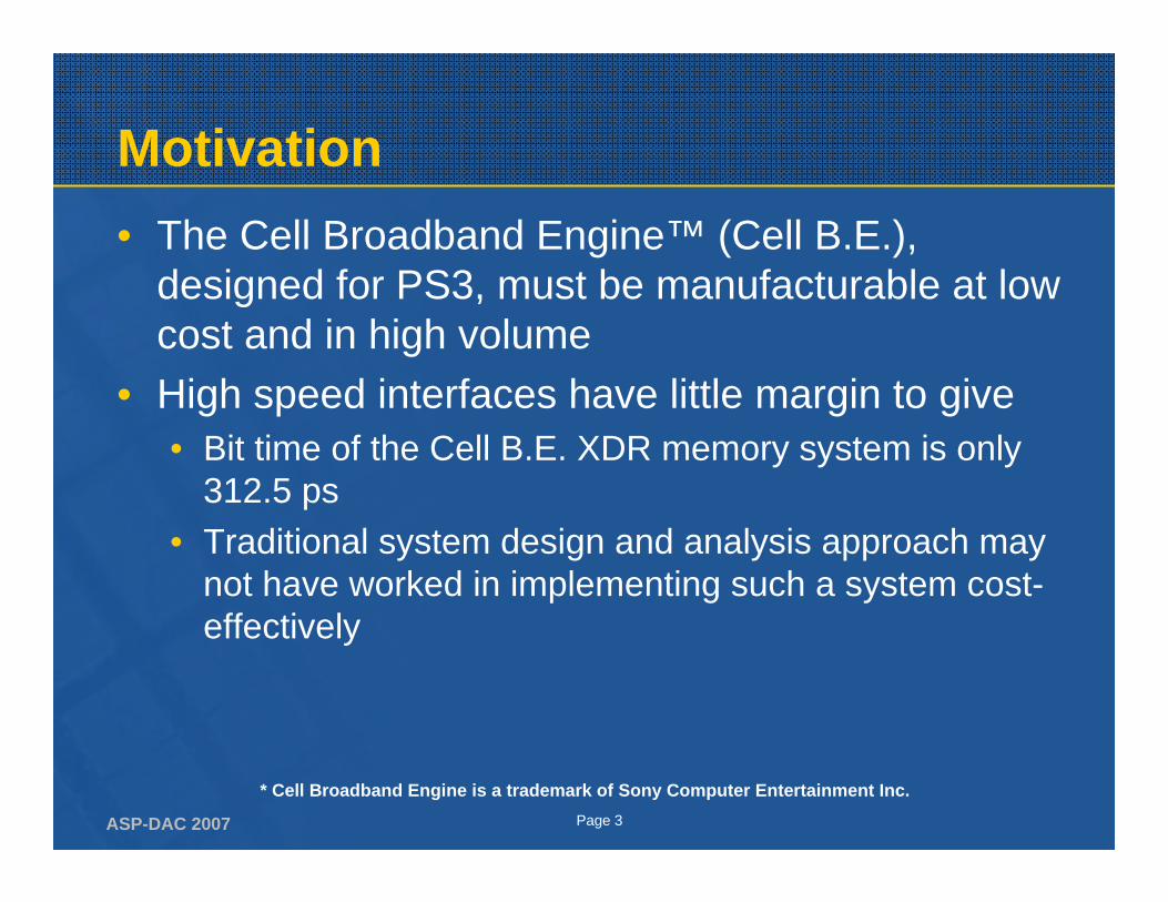
Motivation• The Cell Broadband Engine™ (Cell B.E.),
designed for PS3, must be manufacturable at low cost and in high volume
• High speed interfaces have little margin to give• Bit time of the Cell B.E. XDR memory system is only
312.5 ps• Traditional system design and analysis approach may
not have worked in implementing such a system cost-effectively
* Cell Broadband Engine is a trademark of Sony Computer Entertainment Inc.
ASP-DAC 2007 Page 4
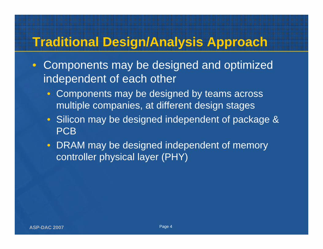
Traditional Design/Analysis Approach• Components may be designed and optimized
independent of each other• Components may be designed by teams across
multiple companies, at different design stages• Silicon may be designed independent of package &
PCB • DRAM may be designed independent of memory
controller physical layer (PHY)
ASP-DAC 2007 Page 5
System Co-Design/Co-Analysis Approach• Different components of the XDR memory
system were designed and analyzed simultaneously• Including XIO, DRAM device, clock chip, packages,
and PCB• System level analysis and optimization performed
taking into consideration interactions between components before the design of any component was finalized
ASP-DAC 2007 Page 6
Merits of Co-Design/Co-Analysis Approach• Allows best trade-off between system cost &
performance• Uncovers potential power integrity and signal
integrity issues at system level early in the design cycle• Allows resolution of such issues with a combination of
architectural, circuit, package, & PCB improvements• Results in solutions with the lowest system cost
ASP-DAC 2007 Page 7
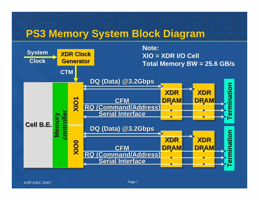
PS3 Memory System Block Diagram
XDR XDR DRAMDRAM
XDR Clock XDR Clock GeneratorGenerator
XDR XDR DRAM DRAM
Cell B.E.Cell B.E.
System Clock
Term
inat
ion
Term
inat
ion
XIO
1XI
O1
Mem
ory
Mem
ory
cont
rolle
rco
ntro
ller
XDR XDR DRAMDRAM
DQ (Data) @3.2GbpsDQ (Data) @3.2Gbps
CFMCFMRQ (Command/Address)RQ (Command/Address)
Serial InterfaceSerial Interface
XDR XDR DRAMDRAM
XDR XDR DRAMDRAMCFMCFM
Serial InterfaceSerial Interface
XIO
XIO
00
Term
inat
ion
Term
inat
ion
XDR XDR DRAM DRAM
XDR XDR DRAM DRAM
XDR XDR DRAM DRAM
Note: XIO = XDR I/O CellTotal Memory BW = 25.6 GB/s
DQ (Data) @3.2GbpsDQ (Data) @3.2Gbps
CTM
RQ (Command/Address)RQ (Command/Address)
ASP-DAC 2007 Page 8
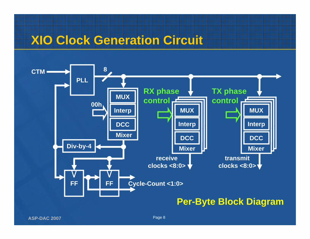
XIO Clock Generation Circuit
MUX
Mixer
Interp
DCC
MUX
Mixer
Interp
DCC
PLL
FF
MUX
Mixer
00h
CTM
receiveclocks <8:0>
Cycle-Count <1:0>
8
Interp
DCC
Div-by-4
MUX
Mixer
Interp
DCC
MUX
Mixer
Interp
DCC
MUX
Mixer
Interp
DCC
MUX
Mixer
Interp
DCC
transmitclocks <8:0>
FF
TX phasecontrol
RX phasecontrol
Per-Byte Block Diagram
ASP-DAC 2007 Page 9
XIO Clock Generation Circuit Features• Both TX (write) and RX (read) mixers for
precision phase control were implemented in the XIO• No phase mixers in the DRAM to keep its cost low
• Each DQ (data) bit has its own independent controls• Data-to-data PCB trace length matching not required
resulting in simpler PCB layout in smaller area
ASP-DAC 2007 Page 10
Power Distribution System Design/Analysis• Power Integrity considered from start of design
process• Power Integrity analyzed at system level
• Every component of the power distribution system included in the model
• Explored different trade-offs to arrive at most cost-effective power distribution system design
ASP-DAC 2007 Page 11
Optimally Accurate Analysis Approach
• Power distribution system consists of multiple components: VRM, PCB, package, chip
• Relative significance of a component in power integrity depends on the noise frequency
• Performed separate power integrity analyses, one for each frequency range
• In each frequency range, simplified models of components whose contribution to power supply noise is relatively small
ASP-DAC 2007 Page 12
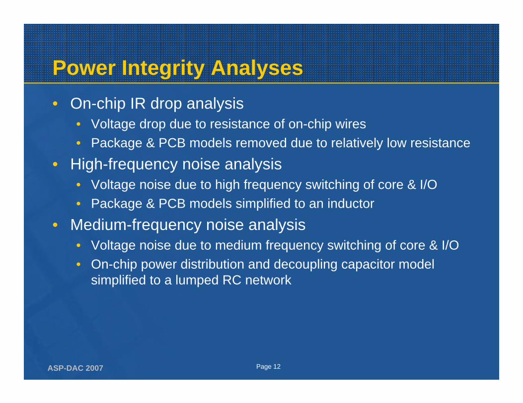
Power Integrity Analyses• On-chip IR drop analysis
• Voltage drop due to resistance of on-chip wires• Package & PCB models removed due to relatively low resistance
• High-frequency noise analysis• Voltage noise due to high frequency switching of core & I/O• Package & PCB models simplified to an inductor
• Medium-frequency noise analysis• Voltage noise due to medium frequency switching of core & I/O• On-chip power distribution and decoupling capacitor model
simplified to a lumped RC network
ASP-DAC 2007 Page 13
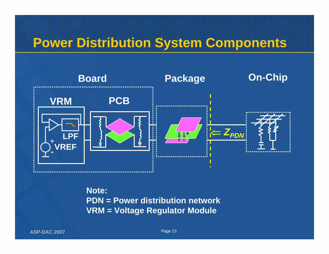
Power Distribution System Components
Board Package On-Chip
⇐ ZPDN
VRM PCB
LPFVREF
+-
Note:PDN = Power distribution networkVRM = Voltage Regulator Module
ASP-DAC 2007 Page 14
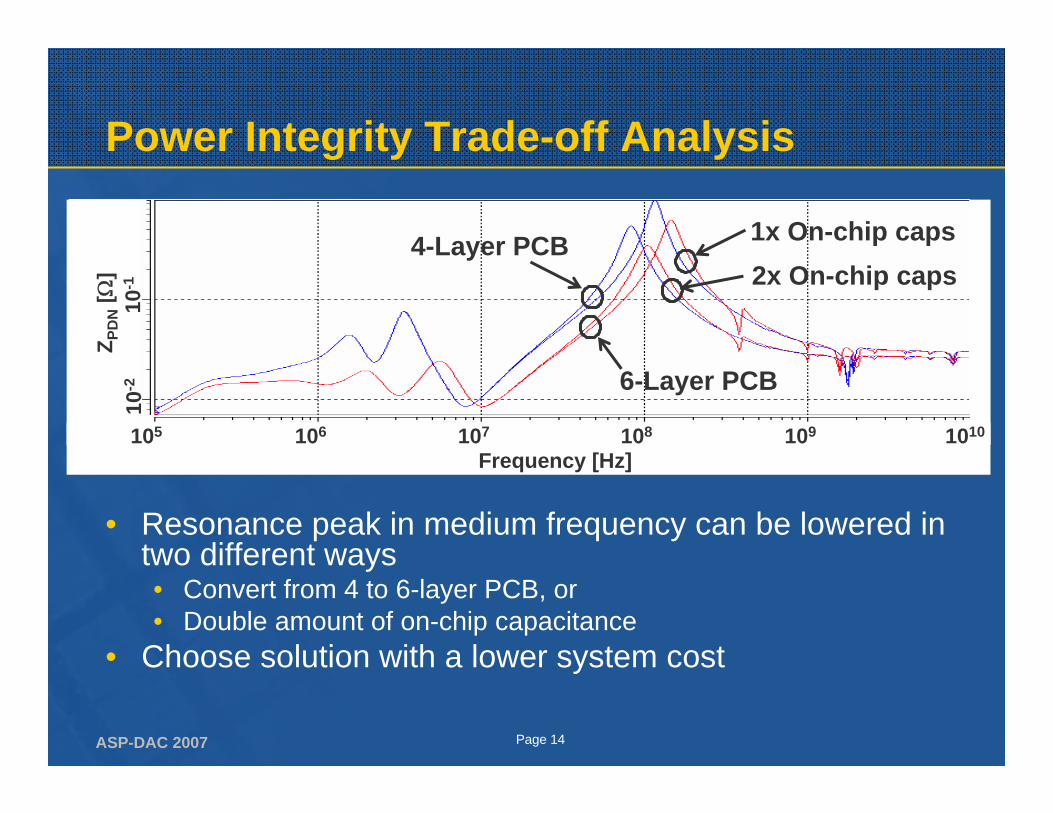
Power Integrity Trade-off Analysis
4-Layer Board
Layer Board
4-Layer PCB
6-Layer PCB
1x On-chip caps2x On-chip caps
Z PD
N[Ω
]10
-210
-1
105 106 107 108 109 1010
Frequency [Hz]
• Resonance peak in medium frequency can be lowered in two different ways• Convert from 4 to 6-layer PCB, or• Double amount of on-chip capacitance
• Choose solution with a lower system cost
ASP-DAC 2007 Page 15
Low Cost Manufacturing Tolerances• Design parameters allowed to vary from their nominal
values within tolerances to minimize manufacturing costs• PCB impedance allowed to vary by ±15%• Package impedance allowed to vary by ±20%
• Such parameter variations result in variations in voltage and timing margins
• Signal integrity analysis to quantify such variations can be computationally expensive
ASP-DAC 2007 Page 16
Statistical Analysis Methods• Statistical signal integrity analysis methods
explored to find an accurate approach with low computational cost
• Taguchi-based method• Uses an orthogonal array to minimize amount of
simulations needed to explore design space• Generates accurate voltage & timing margin
distributions• Provides insight into parameter sensitivities
ASP-DAC 2007 Page 17
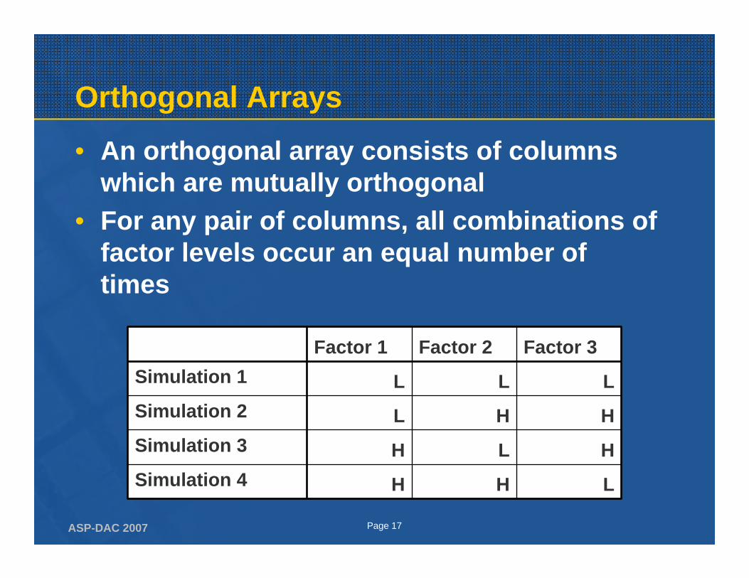
Orthogonal Arrays• An orthogonal array consists of columns
which are mutually orthogonal• For any pair of columns, all combinations of
factor levels occur an equal number of times
H
L
H
L
Factor 2
H
H
L
L
Factor 1
LSimulation 4HSimulation 3HSimulation 2LSimulation 1
Factor 3
ASP-DAC 2007 Page 18
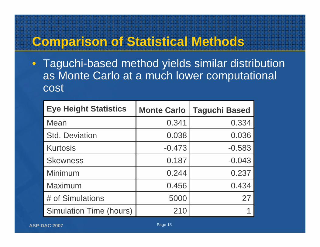
Comparison of Statistical Methods
1210Simulation Time (hours)275000# of Simulations
0.4340.456Maximum0.2370.244Minimum
-0.0430.187Skewness-0.583-0.473Kurtosis0.0360.038Std. Deviation0.3340.341Mean
Taguchi BasedMonte CarloEye Height Statistics
• Taguchi-based method yields similar distribution as Monte Carlo at a much lower computational cost
ASP-DAC 2007 Page 19
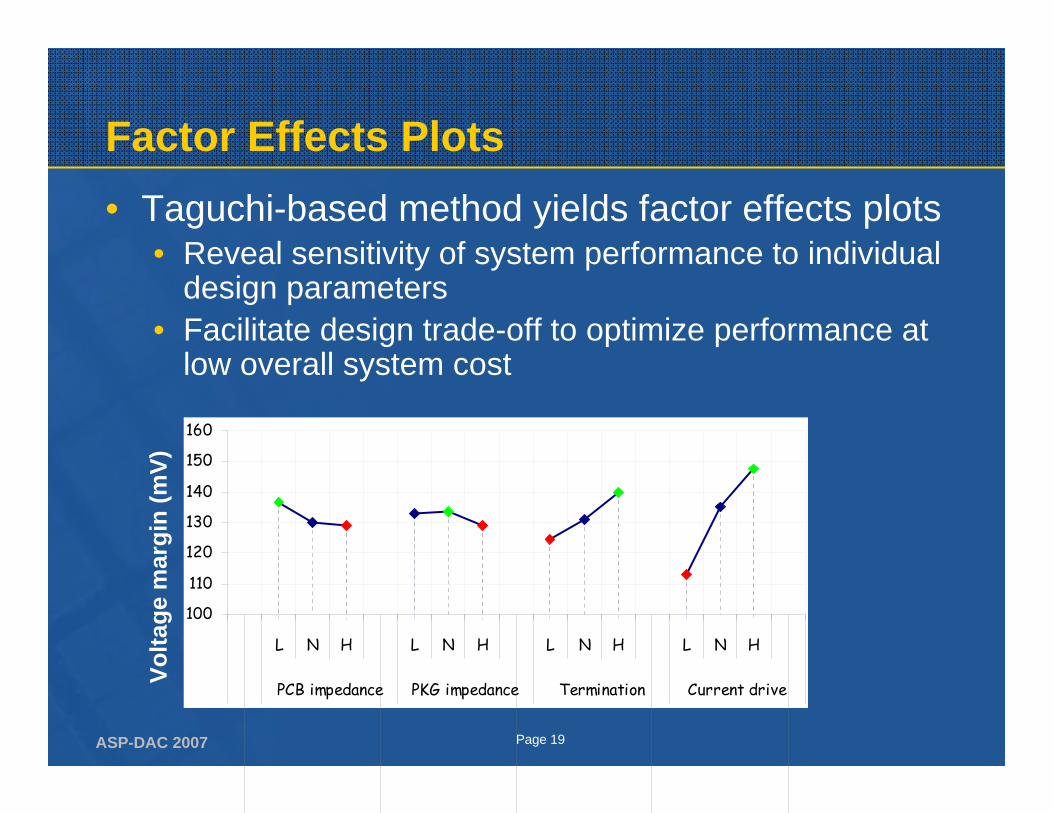
Factor Effects Plots• Taguchi-based method yields factor effects plots
• Reveal sensitivity of system performance to individual design parameters
• Facilitate design trade-off to optimize performance at low overall system cost
100
110
120
130
140
150
160
L N H L N H L N H L N H
PCB impedance PKG impedance Termination Current drive
Volta
ge m
argi
n (m
V)
ASP-DAC 2007 Page 20
Summary• System Co-Design & Co-Analysis approach applied to
the implementation of the XDR memory system of the Cell B.E. processor• Allowed best trade-off between system cost and performance
• Precision phase control circuits implemented in the XIO to lower cost of DRAM and PCB design
• Optimally accurate approach applied to system-level power integrity analysis at low computational cost
• Taguchi-based statistical approach quantified signal integrity variations resulting from manufacturing tolerances at low computational cost