Embed Size (px)
Citation preview

SYSC3601 1 Microprocessor Systems
SYSC3601Microprocessor Systems
Unit 6:Input/Output (I/O) Systems

SYSC3601 2 Microprocessor Systems
Topics/Reading
1. I/O Ports, design, and address decoding.
2. Programmed I/O structures
3. 82C55 - Programmable peripheral interface chip.
Reading: Chapter 11, sections 1-3
Intel specifications: 8255A
SYSC3601 3 Microprocessor Systems
I/O Mapping Options
Two methods are available:
1. I/O mapped I/O (isolated I/O)
I/O Ports are isolated from memory in a separate I/O address space.
Memory can be expanded to full size
Data transfer from/to I/O is restricted to IN and OUT instructions.
Separate control signals using M/IO, WR, RD enable I/O ports.
Intel-based PC’s use isolated I/O
SYSC3601 4 Microprocessor Systems
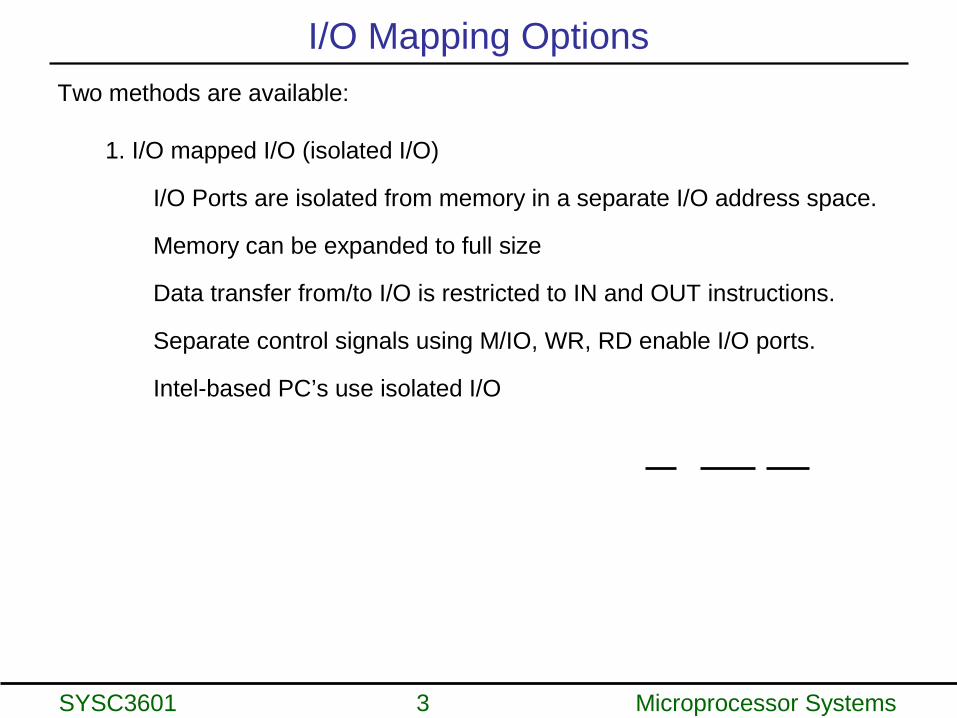
I/O Mapping Options
Two methods are available:
2. Memory Mapped I/O
I/O device is treated as a memory location.
Any memory transfer instruction can used to access the device.
Reduces amount of system memory available to applications.
Reserves fixed portion(s) of the memory map for I/O.
6800, 68000 uses memory-mapped I/O.
SYSC3601 5 Microprocessor Systems
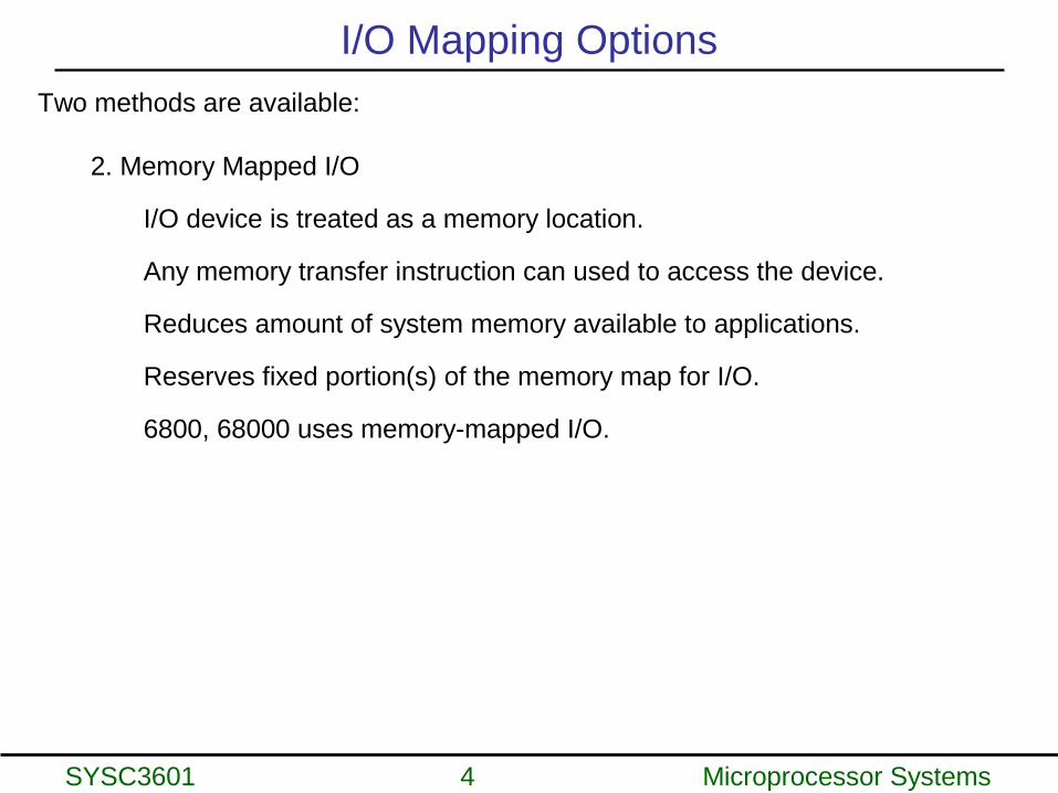
I/O Instructions
8086/8088 provides 2 instructions:IN for I/O Input
OUT for I/O Output
Transfers data between I/O device and the accumulatorEx:
IN AL,45h byte Immediate, fixed 8-bit port
IN AX,46h 16-bit
Immediate
IN AL,DX byte Variable port
IN AX,DX 16-bit
Variable port
OUT 45h,AL
byte Immediate
OUT DX,AX 16-bit
Variable port
SYSC3601 6 Microprocessor Systems
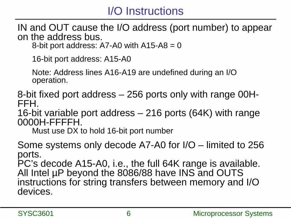
I/O Instructions
IN and OUT cause the I/O address (port number) to appear on the address bus.
8-bit port address: A7-A0 with A15-A8 = 0
16-bit port address: A15-A0
Note: Address lines A16-A19 are undefined during an I/O operation.
8-bit fixed port address – 256 ports only with range 00H-FFH.16-bit variable port address – 216 ports (64K) with range 0000H-FFFFH.
Must use DX to hold 16-bit port number
Some systems only decode A7-A0 for I/O – limited to 256 ports.PC’s decode A15-A0, i.e., the full 64K range is available.All Intel µP beyond the 8086/88 have INS and OUTS instructions for string transfers between memory and I/O devices.
SYSC3601 7 Microprocessor Systems
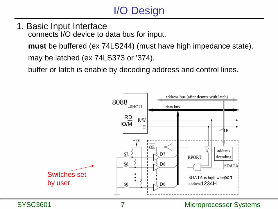
I/O Design1. Basic Input Interface
connects I/O device to data bus for input.
must be buffered (ex 74LS244) (must have high impedance state).
may be latched (ex 74LS373 or ’374).
buffer or latch is enable by decoding address and control lines.
8088
RDIO/M
1234H
16
portSwitches setby user.

SYSC3601 8 Microprocessor Systems
I/O Design
2. Basic Output InterfaceConnects I/O device to data bus for output.
must be latched (ex: 74LS373 or ’374)
latch is enabled (clocked) by decoding address and control lines.
8088
WRIO/M
Lights turn onwhen 1 writtento flip-flop.Why use falling edge?

SYSC3601 9 Microprocessor Systems
I/O Design
3. Latched Input Port + Strobe and StatusExternal device uses strobe input signal to input new data
Status tells µP that new data is waiting (reset by reading data)
8088
RDIO/M
Address decodewill respond to 2addresses andgenerate eitherRSTATUS or RPORT
;assume data port is 1001H;assume status port is 1000H
MOV DX, 1000HLOOP1: IN AL,DX
AND AL,01HJE LOOP1MOV DX, 1001HIN AL,DX
SYSC3601 10 Microprocessor Systems
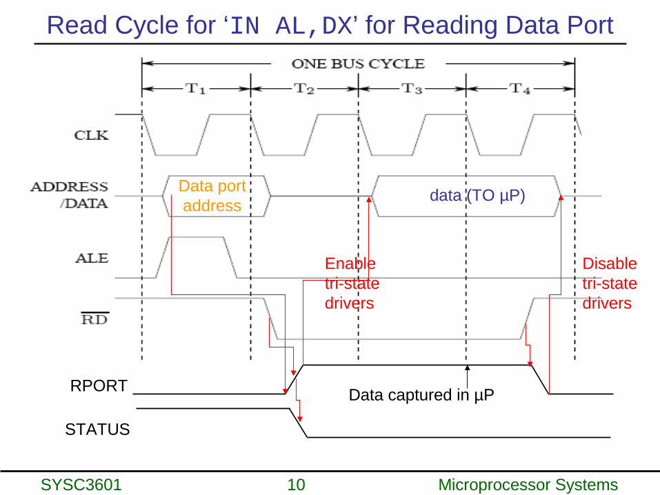
Read Cycle for ‘IN AL,DX’ for Reading Data Port
Data portaddress
data (TO µP)
RPORT Data captured in µP
STATUS
Enable tri-state drivers
Disable tri-state drivers
SYSC3601 11 Microprocessor Systems
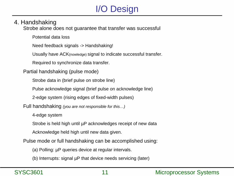
I/O Design4. Handshaking
Strobe alone does not guarantee that transfer was successful
Potential data loss
Need feedback signals -> Handshaking!
Usually have ACK(nowledge) signal to indicate successful transfer.
Required to synchronize data transfer.
Partial handshaking (pulse mode)
Strobe data in (brief pulse on strobe line)
Pulse acknowledge signal (brief pulse on acknowledge line)
2-edge system (rising edges of fixed-width pulses)
Full handshaking (you are not responsible for this…)
4-edge system
Strobe is held high until µP acknowledges receipt of new data
Acknowledge held high until new data given.
Pulse mode or full handshaking can be accomplished using:
(a) Polling: µP queries device at regular intervals.
(b) Interrupts: signal µP that device needs servicing (later)
SYSC3601 12 Microprocessor Systems
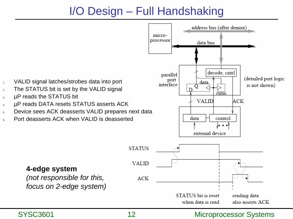
I/O Design – Full Handshaking
1. VALID signal latches/strobes data into port2. The STATUS bit is set by the VALID signal3. µP reads the STATUS bit4. µP reads DATA resets STATUS asserts ACK5. Device sees ACK deasserts VALID prepares next data6. Port deasserts ACK when VALID is deasserted
4-edge system(not responsible for this,focus on 2-edge system)
SYSC3601 13 Microprocessor Systems
I/O Interfacing Example 1
A supervisor control system requires 64 switches and 64 LEDs to be interfaced to an 8088µP. Assumptions and constraints:
1. 8088 is demultiplexed and buffered.
2. each 8-bit input port (switch) and corresponding 8-bit output port (LED) pair is to have the same address.
3. I/O mapped I/O is used with addresses running sequentially from CBF0H-CBF7H.
4. Use decoders, latches, buffers and logic gates as required.
5. Subroutine reads switches and set corresponding LED using programmed I/O (as opposed to interrupts).

SYSC3601 14 Microprocessor Systems
I/O Interfacing Example 1
1) Supervisory Control System Architecture:
SYSC3601 15 Microprocessor Systems
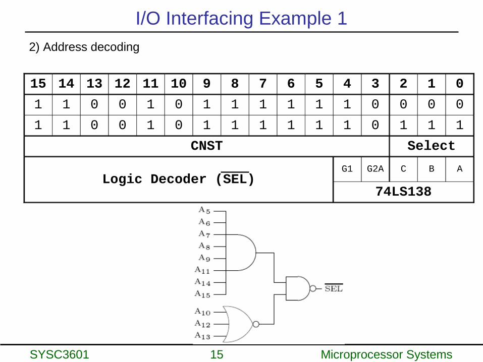
I/O Interfacing Example 1
2) Address decoding
15 14 13 12 11 10 9 8 7 6 5 4 3 2 1 0
1 1 0 0 1 0 1 1 1 1 1 1 0 0 0 0
1 1 0 0 1 0 1 1 1 1 1 1 0 1 1 1
CNST Select
Logic Decoder (SEL)G1 G2A C B A
74LS138

SYSC3601 16 Microprocessor Systems
I/O Interfacing Example 1
3) Interface Design
OE

SYSC3601 17 Microprocessor Systems
I/O Interfacing Example 1
4) OperationMOV DX,CBF4h ; Load port address.IN AL,DX ; Read switches.OUT DX,AL ; Update LED’s
Read:
(a) T1: CBF4h → Address Lines, ‘1’ → IO/M.
(b) ’138 enabled with A2A1A0 = 100; Y4← ‘0’
(c) 74LS244 enabled → switch data appears on D7-D0
(d) T2: ‘0’ → RD
(e) T3: Data read by µP at end of T3.
(f) T4: ‘1’ → RD, address & control de-asserted by µP

SYSC3601 18 Microprocessor Systems
I/O Interfacing Example 1
4) Con’tMOV DX,CBF4H ; Load port address.IN AL,DX ; Read switches.OUT DX,AL ; Update LED’s
Write:
(a) T1: CBF4h → Address Lines, ‘1’ → IO/M
(b) ’138 enabled with A2A1A0 = 100; Y4← ‘0’
(c) T2: ‘0’ → WR, Data on D7-D0
(d) T4: ‘1’ → WR, clocks ’374. D-inputs to Q-outputs.
Address, data & control de-asserted by µP.

SYSC3601 19 Microprocessor Systems
82C55 Programmable Peripheral Interface
Note: 82C55 structure, functions, interfacing is done in class. Software, programming is homework for LAB 2 Prep.General Structure:

SYSC3601 20 Microprocessor Systems
82C55 Programmable Peripheral Interface
Used in PC’s to interface to keyboard and parallel ports.Three I/O Ports, programmed in groups of 12 pins.Group A: PA7–PA0 PC7–PC4Group B: PB7–PB0 PC3–PC0Pins A1 and A0 are used to select an internal register or port.
Access to 82C55: CS=0, the A1A0 determines function.
A1
A0
Function
0 0 Port A
0 1 Port B
1 0 Port C
1 1 Command register (write only)

SYSC3601 21 Microprocessor Systems
I/O Interfacing Example 2
Ex: Interface an 82C55 to an 8086µP so that the I/O ports have the following addresses:
Port A: 00C0Port B: 00C2Port C: 00C4
Command Reg: 00C6
Note that this design will only support 8-bit reads/writes to even port addresses (even though
8086 has a 16-bit data bus).

SYSC3601 22 Microprocessor Systems
I/O Interfacing Example 2
Solution:1. Port addresses:
15 14 13 12 11 10 9 8 7 6 5 4 3 2 1 0
00C0: 0 0 0 0 0 0 0 0 1 1 0 0 0 0 0 0
00C2: 0 0 0 0 0 0 0 0 1 1 0 0 0 0 1 0
00C4: 0 0 0 0 0 0 0 0 1 1 0 0 0 1 0 0
00C6: 0 0 0 0 0 0 0 0 1 1 0 0 0 1 1 0
C C C C C C C C C C C C C A1 A0 C
Decode to enable 82C55 82C55Address Lines
SYSC3601 23 Microprocessor Systems
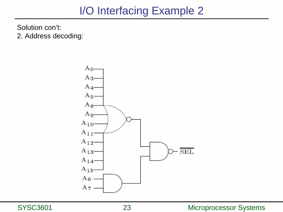
I/O Interfacing Example 2
Solution con’t:2. Address decoding:

SYSC3601 24 Microprocessor Systems
I/O Interfacing Example 2
Solution con’t:3. Design interface:
From 2)
To/fromExternalDevices…

SYSC3601 25 Microprocessor Systems
82C55 Programmable Peripheral InterfaceModes of operation:
Commands are written to the command register port.
3 modes of operation:
Mode 0 Basic I/OTwo 8-bit ports (A&B) and two 4-bit ports (C7-C4 and C3-C0)
Any port can be selected as input or output.
Outputs are latched.
Inputs are NOT latched.

SYSC3601 26 Microprocessor Systems
82C55 Programmable Peripheral Interface
Modes of operation con’t:
Mode 1 Strobed Input/OutputTwo groups:
Group A = Port A & C7-C3
Group B = Port B & C2-C0
8-bit ports A or B can be used for input or output (both latched).
Port C pins can be used for control and status of 8-bit port.
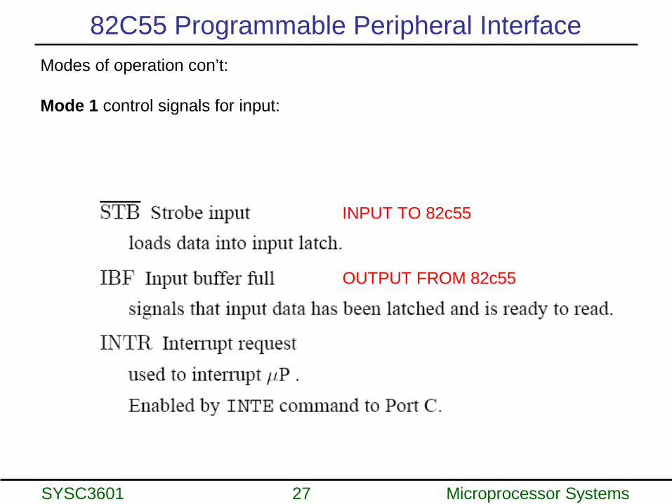
SYSC3601 27 Microprocessor Systems
82C55 Programmable Peripheral Interface
Modes of operation con’t:
Mode 1 control signals for input:
INPUT TO 82c55
OUTPUT FROM 82c55

SYSC3601 28 Microprocessor Systems
82C55 Mode 1 Input Port

SYSC3601 29 Microprocessor Systems
82C55 Mode 1 Input Port
To 8086… To 8086…
To external deviceTo external device
PC
PA PA
PC
External to 82C55: “I’m sending you new data”
82C55 to external: “Data received – don’t send anymore yet”
µP to 82C55: “Got it”
To/From 8086via 8 pins to data bus
From external device
From external device
82C55 to µP : “Come and get it”
82C55 to external: “More please”
From external device From external device
From external device
FROM µP
82C55 82C55

SYSC3601 30 Microprocessor Systems
82C55 Programmable Peripheral Interface
Modes of operation con’t:
Mode 1 control signals for output:

SYSC3601 31 Microprocessor Systems
82C55 Mode 1 Output Port
Could use OBF signalfrom PC1 instead ofgenerating manually viathe PC4 general purpose I/O pin.

SYSC3601 32 Microprocessor Systems
82C55 Mode 1 Output Port
To 8086… To 8086…
To external deviceTo external device
PA
PC
Starting state:- Interrupt has beenrequested.- Must provide newdata to 82C55 toclear the request.
read
SYSC3601 33 Microprocessor Systems
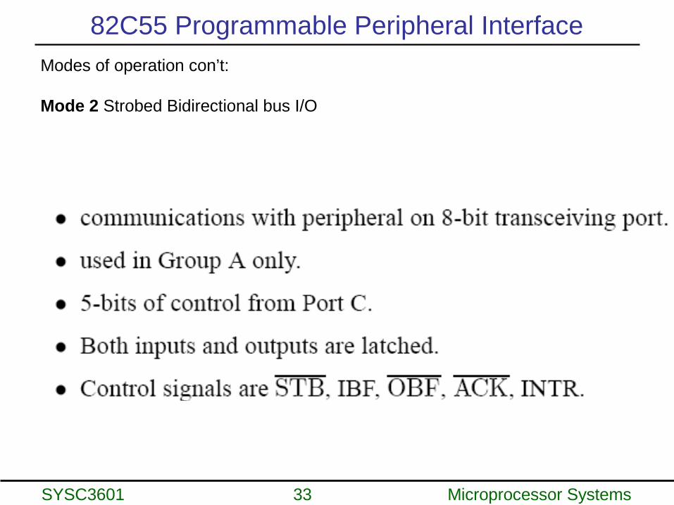
82C55 Programmable Peripheral Interface
Modes of operation con’t:
Mode 2 Strobed Bidirectional bus I/O

SYSC3601 34 Microprocessor Systems
82C55 Mode 2 Bi-directional Port
To 8086…
To external device
To external device
SYSC3601 35 Microprocessor Systems
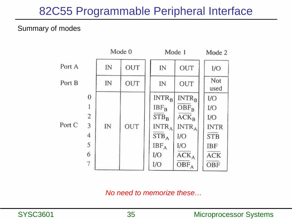
82C55 Programmable Peripheral Interface
Summary of modes
No need to memorize these…