Embed Size (px)
Citation preview

International Research Journal of Engineering and Technology (IRJET) e-ISSN: 2395 -0056
Volume: 04 Issue: 04 | Apr -2017 www.irjet.net p-ISSN: 2395-0072
© 2017, IRJET | Impact Factor value: 5.181 | ISO 9001:2008 Certified Journal | Page 1798
Synthesis and Simulation of a Three Input Binary AND Gate using
Behavioral Level Modelling
Noor Ul Abedin1
1Assistant Professor, Dept. Of Electronics and Communication Engineering, Deccan College of Engineering and
Technology, Telangana State, India
---------------------------------------------------------------------***---------------------------------------------------------------------Abstract - Illustrating the Synthesis and simulation of a
three input binary AND Gate using behavioral level modelling
with considering the output as a register instead of using case
or conditional statements.
The paper is a further advancement my published journal paper “Synthesis and Simulation of Binary AND Gate using Behavioral Level Modelling” in “International Referred Journal of Engineering and Science (IRJES)”. Key Words: AND gate, Verilog HDL1 Behavioral level modelling2, Xilinx 14.7, Synthesis and Simulation.
1. INTRODUCTION Basically we all are familiar with binary logic gates as these
are the building blocks of digital circuits either complex or
simple.
So basically here I am showing how a very important
multiplicative operative i.e. a binary AND with three inputs
can be implemented by CAD tools i.e. is synthesised and
simulated using Xilinx 14.7 software.
1 Verilog HDL, standardized as IEEE 1364, is a
behavioural and a structural case- sensitive hardware
description language (HDL) used to model electronic
systems. It is most commonly used in the design and
verification of digital circuits at the register-transfer
level (RTL) of abstraction.
2 The module is implemented in terms of desired
design algorithm without concern for the hardware implementation details.
2. CIRCUIT DIAGRAM AND TRUTH TABLE OF A THREE INPUT AND GATE
Fig.1. Circuit Symbol of Three input AND Gate
Table -1: Truth Table of a Three input AND Gate
Input
in1
Input
in2
Input
in3
Output
out
(out=in1.in2.in3)
0 0 0 0
0 0 1 0
0 1 0 0
1 0 0 0
1 1 0 0
0 1 1 0
1 0 1 0
1 1 1 1

International Research Journal of Engineering and Technology (IRJET) e-ISSN: 2395 -0056
Volume: 04 Issue: 04 | Apr -2017 www.irjet.net p-ISSN: 2395-0072
© 2017, IRJET | Impact Factor value: 5.181 | ISO 9001:2008 Certified Journal | Page 1799
3. IMPLEMENTATION In the implementation of a three input AND gate using behavioural level modelling, module name is myandgate with inputs: in1, in2, in3 and output: out. The output here is taken a register continuing with assigning the inputs with always statement and using relative operator to perform logical AND operation.
4. VERILOG HDL DESCRIPTION 4.1. Module Program:
module myandgate(out,in1,in2,in3);
input in1,in2,in3;
output out;
always @ (in1,in2,in3)
begin
out=in1&in2&in3;
end
endmodule
The module program of Verilog HDL serves the purpose for
providing the binary AND gate schematic layout.
4.2. Test Bench/ Simulation Program:
module myandgatetest;
reg in1,in2,in3;
wire out;
myandgate uut (out,in1,in2,in3);
initial
begin
$monitor ($time,”in1=%b,in2=%b,in3=%b,
out=%b”,in1,in2,in3,out);
#100 in1=0; in2=0; in3=0;
#100 in1=0; in2=0; in3=1;
#100 in1=0; in2=1; in3=0;
#100 in1=1; in2=0; in3=0;
#100 in1=1; in2=1; in3=0;
#100 in1=0; in2=1; in3=1;
#100 in1=1; in2=0; in3=1;
#100 in1=1; in2=1; in3=1;
end
endmodule
The simulation/ test bench program associates the module
program to verify the logical combinations of the gate.
5. ANALYSIS ON XILINX 14.7 5.1. Module Program and its obtained Schematic
Fig.2. Module Program in Xilinx
Fig.3. Synthesised Output

International Research Journal of Engineering and Technology (IRJET) e-ISSN: 2395 -0056
Volume: 04 Issue: 04 | Apr -2017 www.irjet.net p-ISSN: 2395-0072
© 2017, IRJET | Impact Factor value: 5.181 | ISO 9001:2008 Certified Journal | Page 1800
5.2. Test Bench/ Simulation Program and its obtained logical Simulated Verification Outputs
Fig.4. Simulation Program
Observed Simulated Outputs:
a. With inputs in1=0, in2=0, in3=0 and output
out=0
Fig. 5.1.
b. With inputs in1=0, in2=0, in3=1 and output out=0
Fig. 5.2.
c. With inputs in1=0, in2=1, in3=0 and output out=0
Fig. 5.3.

International Research Journal of Engineering and Technology (IRJET) e-ISSN: 2395 -0056
Volume: 04 Issue: 04 | Apr -2017 www.irjet.net p-ISSN: 2395-0072
© 2017, IRJET | Impact Factor value: 5.181 | ISO 9001:2008 Certified Journal | Page 1801
d. With inputs in1=1, in2=0, in3=0 and output out=0
Fig. 5.4.
e. With inputs in1=1, in2=1, in3=0 and output
out=0
Fig. 5.5.
f. With inputs in1=0, in2=1, in3=1 and output out=0
Fig. 5.6.
g. With inputs in1=1, in2=0, in3=1 and output out=0
Fig. 5.7.
International Research Journal of Engineering and Technology (IRJET) e-ISSN: 2395 -0056
Volume: 04 Issue: 04 | Apr -2017 www.irjet.net p-ISSN: 2395-0072
© 2017, IRJET | Impact Factor value: 5.181 | ISO 9001:2008 Certified Journal | Page 1802
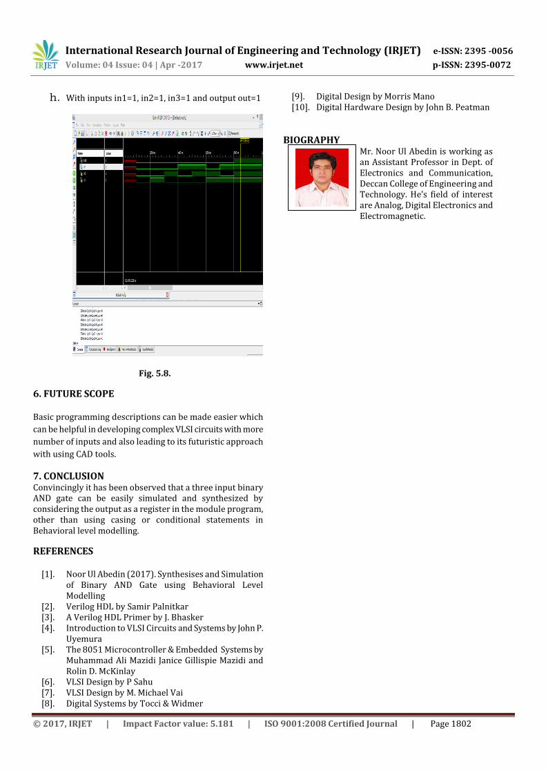
h. With inputs in1=1, in2=1, in3=1 and output out=1
Fig. 5.8.
6. FUTURE SCOPE Basic programming descriptions can be made easier which
can be helpful in developing complex VLSI circuits with more
number of inputs and also leading to its futuristic approach
with using CAD tools.
7. CONCLUSION Convincingly it has been observed that a three input binary AND gate can be easily simulated and synthesized by considering the output as a register in the module program, other than using casing or conditional statements in Behavioral level modelling.
REFERENCES
[1]. Noor Ul Abedin (2017). Synthesises and Simulation of Binary AND Gate using Behavioral Level Modelling
[2]. Verilog HDL by Samir Palnitkar [3]. A Verilog HDL Primer by J. Bhasker [4]. Introduction to VLSI Circuits and Systems by John P.
Uyemura [5]. The 8051 Microcontroller & Embedded Systems by
Muhammad Ali Mazidi Janice Gillispie Mazidi and Rolin D. McKinlay
[6]. VLSI Design by P Sahu [7]. VLSI Design by M. Michael Vai [8]. Digital Systems by Tocci & Widmer
[9]. Digital Design by Morris Mano [10]. Digital Hardware Design by John B. Peatman
BIOGRAPHY
Mr. Noor Ul Abedin is working as an Assistant Professor in Dept. of Electronics and Communication, Deccan College of Engineering and Technology. He’s field of interest are Analog, Digital Electronics and Electromagnetic.