Embed Size (px)
Citation preview

Pag
e1
yyu
SYNTHESIS AND CHARACTERISATION OF COPPER
SELENIDE NANOPARTICLES VIA EMULSION TECHNIQUE
By
CHONG WEI SOON
A project report submitted to the Department of Chemical Science
Faculty of Science,
Universiti Tunku Abdul Rahman,
In partial fulfillment of requirements for the degree of
Bachelor of Science (Hons) Chemistry
May 2011

Pag
eii
yyu
ABSTRACT
Copper selenide (CuSe) nanoparticles had been successfully synthesised by using
copper(II) chloride dihydrate (CuCl2 ∙ 2H2O) and sodium selenite (Na2SeO3) in
ternary oil-in-water (o/w) emulsion system. The reducing agent, sodium
borohydride (NaBH4) used to reduce sodium selenite source in synthesising CuSe
at room temperature. The sizes of the CuSe nanoparticles were determined by X-
Ray diffractometer. Visible optical spectroscopy study was carried out to
determine the band gap of the nanostructure CuSe and also to understand the
quantum confinement of the CuSe. The crystallite size of synthesised CuSe
samples are around 8.0447 – 20.2958 nm. The band gap energy was found in the
range of 1.87 – 2.40 eV. Besides that, the samples were also examined with
Photoluminescence (PL) Spectrophotometer and an emission peak was observed
in the visible range at about 438 nm.

iii
ABSTRAK
kuprum selenide (CuSe) nanopartikel telah berjaya disintesis dengan tindak balas
antara kuprum klorida-dihidrat (CuCl2 ∙ 2H2O ) dan natrium selenite (Na2SeO3)
dalam sistem emulsi. Agen penurunan NaBH4 (Natrium Borohidrida)telah
digunakan untuk sintesis CuSe pada suhu bilik. Spektrometer pembelauan sinar-X
(XRD) telah digunakan untuk menentukan band gap CuSe nanostruktur. Saiz
kristal yang sampel CuSe disintesis adalah di antara 8.0447 – 20.2958 nm. Tenaga
band gap yang ditemui adalah dalam lingkungan di antara 1.87 – 2.40 eV. Selain
itu, Spektrometer Fotoluminisasi juga telah digunakan untuk menganalisiskan
sampel-sampel tersebut. Puncak spektrum untuk kesemua spektrum telah didapati
pada panjang gelombang sekitar 438 nm.

iv
ACKNOWLEDGEMENTS
I will begin my acknowledgement by sincerely thanking my supervisor, Dr.
Saravanan Nagalingam for his guidance during the period of completing this
project by providing numerous suggestions and valuable knowledge. His patience
in guiding and continuous help was the main essence that keeps me working till
the end. I would also like to express my gratitude to him for grating me freedom
and positive attitude in completing this research.
Secondly, I would like to thank my fellow research team mates - Yong Siok San
and Leong Kah Meng as well as laboratory assistant for their valuable comments
and ideas on this work. Next, special thanks also go to Edwin kam, Bee Chong,
Ar Qing, Mean Chuan and those who have helped me for being so supportive and
keep me motivated along the way.
I would like to take this opportunity to thank my parents and siblings for giving
me support constantly to overcome all the obstacles faced in completing this
project and the degree of program.

v
APPROVAL SHEET
I certify that, this project entitled “SYNTHESIS AND CHARACTERISATION
OF COPPER SELENIDE NANOPARTICLES VIA EMULSION TECHNIQUE”
was prepared by CHONG WEI SOON and submitted in partial fulfillment of the
requirements for the degree of Bachelor of Science (Hons) in chemistry at
Universiti Tunku Abdul Rahman.
Approved by
Supervisor
Date:
(Dr. Saravanan Nagalingam)
Assistant Professor

vi
FACULTY OF SCIENCE
UNIVERSITI TUNKU ABDUL RAHMAN
Date:
PERMISSION SHEET
It is hereby certified that CHONG WEI SOON (08ADB06252) has completed this
report entitled “SYNTHESIS OF COPPER SELENIDE NANOPARTICLES
USING EMULSION TECHNIQUE” under supervisor of ASSISTANT
PROFERSSOR DR. SARAVANAN NAGALINGAM from the Department
Chemical Science, Faculty of Science.
I hereby give permission to my supervisor to write and prepared manuscript of
these research findings for publishing in any form, if I did not prepare it within six
(6) months‟ time from this date provided that my name is included as one of the
authors for this article. Arrangement of the name depends on my supervisor.

vii
DECLARATION
I hereby declare that this project report is based on my original work except for
citations and quotations which have been duly acknowledged. I also declare that it
has not been previously and concurrently submitted for any other degree or award
at UTAR or other institutions.
CHONG WEI SOON
Date:

viii
TABLE OF CONTENTS
Page
ABSTRACT ii
ABSTRAK iii
ACKNOWLEDGEMENT iv
APPROVAL SHEET v
PERMISSION SHEET vi
DECLARATION vii
LIST OF TABLES xi
LIST OF FIGURES xii
LIST OF ABBREVIATION xvi
CHAPTER
1. INTRODUCTION 1
1.1. Nanotechnology 1
1.2. Nanometer 1
1.3. Nanomaterial 2
1.3.1. One-dimension Nanomaterials (1-D) 3
1.3.1.1 Thin Films, layers and surfaces 3
1.3.2 Two-dimensional Nanomaterials (2-D) 4
1.3.2.1 Carbon Nanotubes 4
1.3.2.2 Nanowires 6
1.3.3 Three-dimensional Nanomaterials (3-D) 6
1.3.3.1 Quantum dots 6
1.3.3.2 Nanoparticles 9
1.3.4 Effect of the Changes in Dimension 10
1.3.4.1 Changes to the system total energy 10
1.3.4.2 Changes to the system structure 11

ix
1.4 Applications of Nanotechnology 11
1.4.1 Sunscreens and Cosmetics 12
1.4.2 Catalysts 12
1.4.3 Tougher and harder Cutting tools 13
1.4.4 Heterogeneous nanostructures & composites 13
1.4.5 Sensors 14
1.4.6 Therapeutic drugs 14
1.4.7 Drugs delivery 15
1.4.8 Optical electronics 15
1.4.9 Transistor 15
1.5 Fabrication methods 16
1.5.1 Top down approach 17
1.5.2 Bottom up approach 17
1.5.3 Template growth of nanomaterials 18
1.5.3.1 Differences of Microemulsion & emulsion system 18
1.6 CuSe and Its application 20
1.7 Objectives 21
2 LITERATURE REVIEW 22
2.1 Microemulsion and the Formation of Micelles Structure 22
2.2 Effect of CTAB on the formation of nanoparticle 25
2.3 Water/oil volume ratio effects on the formation of
CuInSe2 27
2.4 Duration effects on the microstructures of CuInSe2
Powders 29
2.5 Effect of reaction temperature on the microstructures
of CuInSe2 powders 32
2.6 Template free-solvothermaly synthesised copper selenide
(CuSe, Cu2_xSe, b-Cu2Se and Cu2Se) hexagonal
nanoplates from different precursors at low temperature 34
2.7 The effect of annealing on vacuum-evaporated copper
selenide and indium telluride thin films 35
2.8 Physical, optical and electrical properties of copper
selenide (CuSe) thin films deposited by solution growth
technique at room temperature 37
2.9 Optical properties and electrical conductivity studies
of copper selenide nanoparticle 39
2.10 Photon absorption in direct and indirect band gap
Semiconductor 41

x
3 METHODOLOGY 42
3.1 Chemical used 42
3.2 Apparatus 42
3.3 Synthesis of Copper Selenide using Ternary Water-in-oil
emulsion system 43
3.3.1 Effect of reducing Agent Concentration 43
3.3.2 Effect of stirring 46
3.3.3 Effect of autoclaved period 47
3.3.4 Centrifugation of samples 48
3.4 Characterisation 49
3.4.1 X-ray Diffraction (XRD) 50
3.4.2 Optical Properties 53
3.4.3 Photoluminescence (PL) Spectrophotometer 55
4 RESULTS AND DISCUSSION 57
4.1 X-Ray Diffractometer 57
4.2 UV/Vis spectrometer (optical properties) 70
4.3 Photoluminescence Spectrophotometer 79
5 CONCLUSION AND RECOMMENDATIONS 84
BIBLIOGRAPHY 86
APPENDICES 93

xi
LIST OF TABLES
Table page
1.1 Comparison of emulsion and microemulsion 19
2.1 The optical band gap was measured at room temperature for CuSe 41
3.1 Chemical used to synthesis Copper selenide (CuSe) nanoparticles 42
3.2 Preparation of sample at various concentrations of reducing agent
(NaBH4) 44
3.3 Preparation of CuSe sample at different period (time of stirring) 46
3.4 Preparation of CuSe sample at various heated-treatment periods 47
4.1 XRD data for sample prepared at various reducing agent
concentration 61
4.2 XRD data for sample prepared at various stirring period 63
4.3 XRD data for sample prepared at various heated-treatment period 65
4.4 Comparison of mean crystallite size for seven samples 67
4.5 Comparison of band gap energy values of samples prepared and
literature band gap energy values 78
4.6 Summary of the emission peak and fluorescence intensity for all
samples prepared in different parameters 79

xii
LIST OF FIGURES
Figure page
1.1 The comparison of size with different matters 2
1.2 Molecular structures of a single-walled carbon nanotube
(SWNT) and of a multi-walled carbon nanotube (MWNT) 5
1.3 The band diagram for nano-sized crystals of semiconductor
(quantum dots) 7
1.4 Colloidal quantum dots irradiated with a UV light. Different
sized quantum dots emit different color light due to quantum
confinement. 8
1.5 Nanoparticles in water suspension exhibit different colours
depending on the size and shape 10
1.6 Schematic representation of the building up of Nanostructures 16
2.1 Structure of inverse micelle and normal micelle 23
2.2 Comparison between water in oil emulsion and oil in water
Emulsion 24
2.3 XRD patterns of CuInSe2 powders prepared at 200 °C for 3 h
with the W/O volume ratios of (a) 1:5, (b) 1:10, and (c) 1:15
in the microemulsion-mediated solvothermal process 28
2.4 XRD patterns of CuInSe2 powders prepared at 200 °C for (a)
30 min, (b) 1 h, (c) 3 h, and (d) 5 h with the W/O volume ratio of
1:15 in the microemulsion-mediated solvothermal process 30
2.5 TEM micrographs of CuInSe2 powders prepared at 200 °C for (a)
30 min, (b) 1 h, (c) 3 h, and (d) 5 h with the W/O volume ratio of
1:15 in the microemulsion-mediated solvothermal process 31

xiii
2.6 XRD patterns of CuInSe2 powders prepared at (a) 160 °C, (b)
180 °C, (c) 200 °C, and (d) 220 °C for 3 h with the W/O volume
ratio of 1:15 in the microemulsion-mediated solvothermal process 33
2.7 TEM micrographs of CuInSe2 powders prepared at (a) 160 °C,
(b) 180 °C, (c) 200 °C, and (d) 220 °C for 3 h with the W/O
volume ratio of 1:15 in the microemulsion-mediated
solvothermal process 33
2.8 X-ray diffractogram of as-deposited and 473 K annealed
CuSe films 36
2.9 Plot of (αhν)2 vs. hν for CuSe thin films 38
2.10 The relation between absorbance and wavelength for CuSe
Prepared at T=160 °C, T=170 °C and T=200 °C dispersed
in absolute ethanol 39
2.11 Relation between (αhν)2 and photon energy (hν) for CuSe
prepared at T=160 °C, 170 °C and T=200 °C 40
2.12 E-k diagram illustrating a) Photon absorption in a direct band gap
semiconductor b) Photon absorption in an indirect band gap
semiconductor assisted by phonon absorption and c) Photon
absorption in an indirect band gap semiconductor assisted by
phonon emission. 41
3.1 Flowchart of sythesising CuSe at various concentration of
reducing agent, NaBH4 45
3.2 Centrifugation instrument model Sigma Sartorius 2-1 48
3.3 Shimadzu X-ray Diffractometer (LabX XRD-6000) 50
3.4 Diagram for Bragg reflection from a set of crystal planes with a
spacing of d 51
3.5 A schematic diagram of a powder diffractometer 52
3.6 Perkin Elmer Lambda 35 UV/Vis Spectrophotometer 53

xiv
3.7 Diagram of double beam UV/Vis spectrometer 54
3.8 Fluorescence Spectrophotometer, Pelkin Elmer Precisely LS 55 55
3.9 Energy level diagram of fluorescence occurrence 56
4.1 Formation of micelle system in synthesis of copper selenide
nanoparticles 58
4.2 XRD pattern of samples prepared at various reducing agent
concentration, [NaBH4]M 60
4.3 XRD pattern of samples prepared at various periods
(under stirring condition) 62
4.4 XRD pattern of samples prepared at various periods
(under autoclave condition) 64
4.5 UV/Vis absorption spectrum of CuSe nanoparticles at different
concentration of reducing agent S3020 = 2.0 M, S3025 = 2.5 M,
S3030 = 3.0 M, respectively 70
4.6 UV/Vis absorption of CuSe nanoparticles prepared at different
period (under stirring condition) S3020 = 1 hour,
S30202 = 2 hours and S30203 = 3hours 71
4.7 UV/Vis absorption of CuSe nanoparticles prepared at different
period (under autoclave condition) S3020 = 30 minutes,
S6020 = 60 minutes, and S9020 = 90 minutes 72
4.8 Relation between (αhv)2 and photon energy (hv) for CuSe
nanoparticle prepared at various reducing agent, NaBH4
S3020 = 2.0 M, S3025 = 2.5 M and S3030 = 3.0 M 75
4.9 Relation between (αhv)2 and photon energy (hv) for CuSe
nanoparticle prepared at various time of stirring
S3020 = 1 h, S30202 = 2 h and S30203 = 3h 76
4.10 Relation between (αhv)2 and photon energy (hv) for CuSe
nanoparticle prepared at various time of stirring
S3020 = 30 mins, S6020 = 60mins and S9020 = 90 mins 77

xv
4.11 Photoluminescence spectrum of control set for the synthesis of
copper selenide 80
4.12 PL spectra of all the CuSe samples prepared at different
concentration of reducing agent used 80
4.13 PL spectra of all the CuSe samples prepared at different
stirring period 81
4.14 PL spectra of all the CuSe samples prepared at different
heated-treatment period 81

xvi
LIST OF ABBREVIATIONS/ SYMBOLS
CuCl2 ∙ 2H2O Copper(II) chloride dihydrate
Na2SeO3 Sodium selenite
C19H42BrN N-Cetyl-N,N.N-trimethylammonium Bromide
C6H12 Cyclohexane
NaBH4 Sodium borohydride
C2H5OH Absolute ethanol
CMC Critical Micelle Concentration
o/w oil in water
w/o water in oil
XRD X-Ray Diffractometer
UV-Vis UV-visible
PL Photoluminescence
Å Angstrom (10-10
m)
α Alpha
β Beta
γ Gamma
π Pi
λ Lambda
θ Theta

xvii
oC Degree in Celsius
eV Electron Volt
g Gram
m Mili
M Concentration in molL-1
mL Mililiter
nm Nanometer (10-9
m)
μm Micrometer (10-6
m)
At% Percentage of atom
E Energy
h Plank‟s constant (6.63 x 10⁻³⁴
Js)
c Speed of light (3.0 x 10⁸ ms
-1)
ν Velocity

Pag
e1
yyu
CHAPTER 1
INTRODUCTION
1.1 Nanotechnology
Nanoscience is the study of phenomena and manipulation of material at
the nanoscale; it is an extension of existing sciences into the nanoscale (Dutta and
Gupta, 2008).
Nanotechnology refers to technological study and application involving
nanoparticles. It is manipulating matter on an atomic and molecular scale and
dealing with structures sized between 1 to 100 nanometers in at least one
dimension, and involves developing materials or devices within that size.
Nanotechnology may be able to create many new materials and devices with a
vast range of applications, such as in medicine, electronics, biomaterials and
energy production (Asiyanbola and Soboyejo, 2008). Nanoparticle has been
applied loosely to include all particles less than 1 micrometer.
1.2 Nanometer
Nanometer is a unit of spatial measurement that is 10-9
meter. It is
commonly used in nanotechnology, the building of extremely small machines. A

2
nanometer in size of substance can be seen by using powerful microscope like
Atomic Force Microscope. Atoms and molecules and the smallest pieces of
everything around us, are measured in nanometers (Monasi, 2008). The Figure 1.1
below shows the comparison of size of different items.
Figure 1.1: The comparison of size with different matters (adapted from:
http://nanoscience.massey.ac.nz/)
1.3 Nanomaterials
Nanomaterials are not simply another step in the miniaturization of
materials. They can be metals, ceramics, polymeric materials, or composite
materials. Their defining characteristic is a very small feature size in the range of
1-100 nanometers (nm). The nano-world is in between the scale of atomic and
quantum phenomena as well as the scale of bulk materials. At its level, some

3
material properties are affected by the laws of atomic physics, rather than
behaving as traditional bulk materials do. They require very different production
approaches. There are several processes to create nanomaterials, classified as
„top-down‟ and „bottom-up‟ which will be discussed below in detail. Below we
outline some examples of nanomaterials:
1.3.1 One-dimension Nanomaterials (1-D)
1.3.1.1 Thin Films, layers and surfaces
One-dimensional nanomaterials such as thin films and engineered surfaces
have been used for electronic device manufacture, chemistry and engineering. In
the silicon integrated-circuit industry, for example, many devices depend on thin
films for their operation, and control of film thicknesses approaching the atomic
level is routine. Monolayers (layers that are one atom or molecule deep) are also
routinely made and used in chemistry. The formation and properties of these
layers are reasonably well understood from the atomic level upwards, even in
quite complex layers (such as lubricants). Advances are being made in the control
of the composition and smoothness of surfaces, and the growth of films (Smart
and Moore, 2005).
Furthermore, the development of electronics using organic compounds has
led to nanofilm electronic devices. Such films can be applied in computer monitor

4
as flat-screen displays. Technically, there are two types of displays being used in
this industry which are thin-film transistor liquid-crystal display (TTF-LCD) and
organic light-emitting diodes (OLEDs). With the aid of this nanotechnology, a
thinner, lighter, and more flexible screen can be produced when the bank of
transistors is a film of organic material of 20 nm thick instead of a 2 mm thick
layer of silicon (Smart and Moore, 2005).
Engineered surfaces with tailored properties such as large surface area or
specific reactivity are used routinely in a range of applications such as in fuel cells
and catalysts. The large surface area provided by nanoparticles, together with
their ability to self assemble on a support surface, could be of use in all of these
applications(Smart and Moore, 2005).
1.3.2 Two-dimensional Nanomaterials (2-D)
1.3.2.1 Carbon Nanotubes
Two-dimensional (1D) nanostructures such as carbon nanotubes and
semiconductor nanowires have received considerable attention due to their
potential applications in electronic, optical and energy conversion devices. The
electrical, mechanical properties as well as thermal properties have been
investigated at a single nanotube level. However, most of the studies only include
estimating the thermal properties of carbon nanotubes from the experiments of
micrometer-millimeter-sized mats of carbon nanotubes (Zhang et al., 2006).

5
Carbon nanotubes (CNTs) were first discovered by Sumio Iijima in 1991.
It is produced by rolling a graphene (a single sheet of graphite) sheet (Pradeep,
2008) and is thin cylinders of carbon atoms that are both mechanically strong and
highly conducting (Atkins and Paula, 2006). There are two kinds of CNTs which
are single-walled nanotube (SWNT) and multi-walled nanotube (MWNT) which
were shown in Figure 1.2. Single-walled nanotubes have diameters of about 1 nm,
and lengths of the order of 10-6
m. These tubes are capped at each end by half of
fullerene-type structure and have remarkable properties that can be used for a
variety of high performance application because they are very strong
mechanically, flexible and can conduct electricity extremely well (Tang et al.,
2001). Furthermore, they can absorb 100 times their volume of hydrogen and
hence could be applied as a safe storage medium of hydrogen for fuel cells
(Silberberg, 2009). A multi-walled nanotube (MWNT) consists of several
concentric SWNTs and its diameter varies between 2-25 nm (Atkins and Paula,
2006).
Figure 1.2: Molecular structures of a single-walled carbon nanotube (SWNT)
and of a multi-walled carbon nanotube (MWNT). (adapted from
http://www-ibmc.ustrasbg.fr/ict/vectorisation/nanotubes_eng.shtml)

6
1.3.2.2 Nanowires
Nanowires are ultra fine wires or linear arrays of dots with lengths of several
micrometres and diameters of less than 20 nm (Have, 2007), formed by self-
assembly. The synthesis of nanowire, nanometer-sized atomic assemblies that
conduct electricity, is a major step in the fabrication of nanodevice (Atkins and Paula,
2006). Semiconductor nanowires made of silicon and indium phosphides have
demonstrated remarkable optical, electronic and magnetic characteristics for example;
silica nanowires can bend light around very tight corners. Nanowires have potential
applications in high-density data storage; either as magnetic read heads or as
patterned storage media, electronic and opto-electronic nanodevices. The preparation
of these nanowires relies on sophisticated growth techniques, which include self
assembly processes, where atoms arrange themselves naturally on stepped surfaces,
chemical vapour deposition (CVD) onto patterned substrates, electroplating or
molecular beam epitaxy (MBE). The „molecular beams‟ are typically from thermally
evaporated elemental sources.
1.3.3 Three-dimensional Nanomaterials (3-D)
1.3.3.1 Quantum dots
Quantum dots also known as nanocrystals which are specific type of
semiconductor. Quantum dots are sized a few nanometers in diameter and
typically containing 103 to 10
5 atoms and exhibit quantum-size effects (Atkins

7
and Paula, 2006). Due to their electrical characteristics, they are electrically
tunable. The electrical conductivity of semiconductors can change due to external
stimulus such as voltage or exposure to light, etc. As quantum dots have such a
small size they show different properties as compare to bulk material. Quantum
dots are highly light absorbing, luminescent nanoparticles whose absorbance
onset and emission maximum shift to higher energy with decreasing particle size.
This is due to the large band gap of the nano-sized metal in its electron orbital as
compared to the bulk ones. Figure 1.3 has shown that band-gap energy depends
on the composition of the semiconductors as well as the size.
Figure 1.3: The band diagram for nano-sized crystals of
semiconductor (quantum dots) (adapted from:
http://www3.imperial.ac.uk/)

8
If semiconductor particles are made small enough, quantum confinement
effects are observed and its energy level spacing of a nanocrystal exceeds kT
(where k is Boltzmann‟s constant and T is temperature). When Energy differences
more than kT which limit the energies at which electrons and holes (the absence
of an electron) can exist in the particles. As energy is related to wavelength (or
colour), this means that the optical properties of the particle can be finely tuned
depending on its size. Thus, particles can be made to emit or absorb specific
wavelengths (colours) of light, merely by controlling their size which was shown
in Figure 1.4. Recently, quantum dots have found applications in composites,
solar cells and fluorescent biological labels (for example to trace a biological
molecule) which use both the small particle size and tune able energy levels (Bera
et al., 2010).
Figure 1.4: Colloidal quantum dots irradiated with a UV light. Different
sized quantum dots emit different color light due to quantum
confinement. (adapted from: http://www.mdpi.com/1996-1944/3
/4/2260/pdf)

9
1.3.3.2 Nanoparticles
Nanoparticles are grouped as three-dimensional nanocrystals. They are
generally considered to be a number of atoms or molecules bonded together with
a radius of less than 100 nm. A nanometer is 10-9
m or 10Å, so particles having
radius of about less than and equal to 1000Å can be considered to be
nanoparticles. The crystal structure of the nanoparticles is the same as the bulk
structure with somewhat different lattice parameters (Monasi, 2008).
Nanoparticle materials vary depending on their application. Because
nanoparticles are invisible to the naked eye, they are usually supplied suspended
in a liquid. The color is due to the refraction of light the surface area of the
particular nanoparticle reflects. Different sized nanoparticles exhibit different
colors based on its surface area. Therefore, it has been known and used for
centuries in colour stained glass, ceramic glazes and also colloidal gold particles
used to make „ruby‟ glass since Roman times. Metal nanoparticles show peculiar
optical, electronic and magnetic properties that bulk solid or isolated molecules do
not usually exhibit (Capek, 2004). These properties are explained by Atkins and
Paula (2008) as the consequences of their size rather than their chemical
composition. Figure 1.5 shows that nanocyrstals are suspended in water exhibit
different colours depending on its size and shape.

10
Figure 1.5: Nanoparticles in water suspension exhibit different colours
depending on the size and shape (adapted from Bera et al., 2010)
1.3.4 Effect of the Changes in Dimension
1.3.4.1 Changes to the system total energy
Phenomenon of quantum confinement refers to the allowed energy bands
become significantly narrower than in an infinite solid when system size
decreases. The normal delocalized electronic properties of the solid will become
distorted and the electron in this reduced-dimensional system will behave more
like the “particle in box”. Total energy of bulk electronic structure will be affected
by quantum confinement. It is because thermodynamic stability of the reduced
length scales system relative to the normal bulk crystal. It may change the

11
energetically stable of particular materials. For example, nanoparticles to adopt
different crystal structure to normal bulk material. Thus, the changes in the
electronic density of states is possible if the crystallographic structure is adopted
below critical length scale which results in the reduced of total energy system
(Kelsall et al., 2005).
In addition, reduction of system size affect chemical reactivity as well as
physical properties such like electrical, optical, thermal and magnetic
characteristics due to the changes of the arrangement of the outermost electronic
energy levels caused by the reduction of the dimension (Kelsall et al., 2005).
1.3.4.2 Changes to the system structure
The surface area to volume ratio (S/V) and specific surface area of the
system will increase when the dimension of a system decreased, significantly for
those particles less than 100 nm in diameter. This large surface area will have
important implications for the total energy of the system (phenomenon of surface
tension of surface energy due to differences bonding). Thus it leads to the
stabilisation of metastable structures in nanometer-sized systems, which are
different from the normal bulk structure, may induce expansion or contraction of
the normal crystalline lattice that could change other material properties (Kelsall
et al., 2005).

12
1.4 Applications of Nanotechnology
As mentioned above, since nanomaterials possess unique, beneficial
chemical, physical, and mechanical properties, they can be used for a wide variety
of applications. These applications include:
1.4.1 Sunscreens and Cosmetics
Some of the nanosized materials have the properties that they can absorb
and reflect ultraviolet (UV) rays and yet are transparent to visible light and so are
more appealing to the consumer. For example, nanosized titanium dioxide and
zinc oxide are currently used in some sunscreens. However, the use of
nanoparticles in cosmetics has raised a number of concerns about consumer safety
(Nanowerk, 2011).
1.4.2 Catalysts
Nanoparticles have a high surface area, and hence provide higher catalytic
activity as there are more places for other chemical agents to bind and interact for
reaction. Hence, it maximizes the possible reactivity, which is the aim for catalyst.
Nanotechnologies are enabling changes in the degree of control in the production
of nanoparticles, and the support structure on which they reside. It is possible to
synthesise metal nanoparticles in solution in the presence of a surfactant to form
highly ordered monodisperse films of the catalyst nanoparticles on a surface. This
allows more uniformity in the size and chemical structure of the catalyst, which in

13
turn leads to greater catalytic activity and the production of fewer by-products
(Nanowerk, 2011).
1.4.3 Tougher and harder Cutting tools
Cutting tools made of nanocrystalline materials, are much stronger and
harder, much more wear-resistant, erosion-resistant, and last longer than their
conventional counterparts such as tungsten carbide, tantalum carbide and titanium
carbide. Therefore, they enable the manufacturer to machine various materials
much faster, thereby increasing productivity and significantly reducing
manufacturing costs (Nanowerk, 2011).
1.4.4 Heterogeneous nanostructures and composites
Nanoparticles and rigid nanotubes can be used in composites, materials
that combine one or more separate components and which are designed to exhibit
overall the best properties of each component with great fracture strength. This
multi-functionality applies not only to mechanical properties, but extends to
optical, electrical and magnetic ones. Currently, carbon fibres materials and
bundles of multi-walled CNTs are used in polymers to control or enhance
conductivity, with applications such as antistatic packaging (Nanowerk, 2011).

14
1.4.5 High-sensitivity Sensors
Sensors made nanocrystalline materials are extremely sensitive to the
change in their environment. They employ their sensitivity to the changes in
various parameters they are designed to measure. The measured parameters
include electrical resistivity, chemical activity, magnetic permeability, thermal
conductivity, and capacitance. All of these parameters depend greatly on the
microstructure (grain size) of the materials employed in the sensors. A change in
the sensor‟s environment is manifested by the sensor material‟s chemical,
physical, or mechanical characteristics, which is exploited for detection. Typical
applications for sensors made out of nanocrystalline materials are smoke detectors,
ice detectors on aircraft wings, automobile engine performance sensor, etc.
(Nanowerk, 2011).
1.4.6 Therapeutic drugs
Most of these molecular drugs are nanosize, so it becomes more when the drugs
are designed specifically to interact with known biological targets. For example,
the antidepressant is focused on increasing concentration by blocking or
decreasing the destruction of the neurotransmitter molecular (carrier messages) by
modifying their binding properties. So, the concentration of it can be restored to
normal concentration and hence, treat the depression effectively (Nanowerk,
2011).

15
1.4.7 Drugs delivery
Bioavailability of drugs is differing to the concentration of drugs.
Bioavailability refers to the presence of drug molecules where they are needed in
the body. If the drugs delivered directly to the site of a tumour before the tumour
spreads to adjacent organs and without interact to others site, chemotherapy could
become more effectively. Nanotechnology and nanoscience are useful in
increasing bioavailability by encapsulated within the nanoscale cavities inside
polymers within the tablet (Nanowerk, 2011).
1.4.8 Optical electronics
Semiconductors with nanoscale dimension can act as light-emitting
structures. Since their intensity can color can be chosen, these nano sources are
very promising for applications in electronic industry such as flat screen, LED,
cellular phone displays and etc. (Nanowerk, 2011).
1.4.9 Transistor
Nanoscale structures can act as transistors and the individual molecules can
act as field effect transistors. This reduced the size more than 100 times smaller
than those afforded by currently available standard lithography work in silicon.
By combining this transistor with memory devices, allows the processors to be
further reduced in size (Nanowerk, 2011).

16
1.5 Fabrication methods
There are numerous ways to produce a nanostructure product. However,
there are generally divide into two approaches which are top-down approach and
bottom-up approach for synthesis of nano materials which were shown in Figure
1.6. Under controlled conditions, both the top-down and bottom-up approaches
can be viewed as different forms of microstructure engineering.
Figure 1.6: Schematic representation of the building up of Nanostructures.
(adapted from: http://www.gitam.edu/eresource/nano/nanotechnology/role_of_
bottom up_and_topdown_a.htm)

17
1.5.1 Top down approach
The top-down approach is the fabrication method that uses the simple
removal or successive cutting of bulky material to reduce the size down to the
nano-sized particle or structure. On the other hands, it is actually a miniaturization
process of bulky materials. Some of the example methods of top-down approach:
i. Milling of Attrition
ii. Machining
1.5.2 Bottom up approach
In the bottom-up approach, it is a method that uses the atoms, molecules and
even nanoparticles themselves as the building blocks for the creation of the
nanostructure. It means that they build up of a nanostructure material from the
bottom: atom by atom, molecule by molecule or cluster by cluster. The properties
and functionalities of nanostructured materials produced by this method may
possible assist by changing the size of building blocks, controlling their surface
and assembly organisation. Some of the example methods of bottom-up approach:
i. Sol-gel method
ii. Colloidal dispersion methods
iii. Vapour phase deposition methods

18
1.5.3 Template growth of nanomaterials
Template growth of nanometrials is essentially in one of the bottom –up
approaches. It is different from others due to utilizing the principle of wet
chemistry. In this method, usually will to precipitate or deposit a material and
control the growth of nanostructure formed. However, control of the precipitate
size can be difficult and sometimes complicated unless some chemicals are added
to control the precipitates formed. In this case, the nanoparticles growth can be
regulated within self-organised, biological and synthetic organic membranes
assemblies such as micelles, microemulsions, liposomes and vesicles.
1.5.3.1 Differences of Microemulsion and emulsion system
Emulsions are defined as the mixture of two or more immiscible liquids by
any means of mixing method (macroscopically homogeneous and microscopically
heterogeneous). They revert back to two or more phases over time if without the
presence of any supporting substance like emulsifier to withhold (Paul and
Moulik, 2001). Unlike emulsion, microemulsion-processing method is a soft
technique and does not required special instrument or extreme condition (Khiew
et al., 2003). They are low viscosity, large interfacial area and having ability to
solubilise both aqueous phase and oil-soluble compounds (Paul and Moulik,
2001). Furthermore, the system is stabilised by a surfactant film (Lopez-Quintela,
2003). Table 1.1 shows the comparison of emulsion and microemulsion.

19
Table 1.1: Comparison of emulsion and microemulsion
Emulsions
(Macroemulsions)
Microemulsions
Consist of roughly spherical
droplets of one phase dispersed
into the other.
They constantly evolve
between various structures
ranging from droplet like
swollen micelles to
bicontinuous structure.
Droplet diameter: 1 – 20 mm. 10 – 100 nm.
Most emulsions are opaque
(white) because bulk of their
droplets is greater than
wavelength of light and most
oils have higher refractive
indices than water.
Microemulsions are transparent
or translucent as their droplet
diameter are less than ¼ of the
wavelength of light, they scatter
little light.
They may remain stable for
long periods of time, will
ultimately undergo phase
separation on standing to attain
a minimum in free energy.
They are kinetically stable but
thermodynamically unstable.
More thermodynamically stable
than macroemulsions and can
have essentially infinite lifetime
assuming no change in
composition, temperature and
pressure, and do not tend to
separate.
Require intense agitation for
their formation.
Generally obtained by gentle
mixing of ingredients.
(adapted from: http://www.pharmainfo.net/reviews/microemulsions-novel-drug-
delivery-vehicle)

20
1.6 CuSe and Its application
In the past decades, semiconductor nanomaterials have received broad
attentions due to their novel electronic, optical, photoelectric and thermoelectric
properties. As an important semiconductor, copper selenide (CuSe) with
nanostructure has potential applications in various fields, such as optical filter,
highly efficient solar cells, super ionic conductors and thermoelectric converters,
electro-optical devices, photo-thermal conversion, electro-conductive electrodes,
and microwave shielding coating. These materials are semiconductors with p-type
conductivity (Zainal et al., 2004). Thus, many studies about the preparation and
characterisation of CuSe nanostructures have been reported. It may be more
important to find out the properties of CuSe nanostructures because the
applications of CuSe can be derived from these findings (Wei et al., 2007).
Copper selenide is a metal chalcogenide semiconductor with a wide range of
stoichiometric compositions and also with various crystallographic forms for each
of these compositions. The synthesis of this material in thin film form has been
described by using different deposition method such as chemical bath deposition
(CBD) selenisation, flash evaporation, vacuum evaporation and spray method,
etc.. Copper selenide exists in widely different crystallographic modifications
even at room temperature such as (orthorhombic, monoclinic and cubic) forms,
depending on the method of preparation.

21
Objectives
The objectives of this project are:
1. To synthesise CuSe nanoparticles using emulsion technique.
2. To characterise the CuSe nanoperticles using X-Ray Diffractometer,UV-
Vis Spectrophotometer and Fluoroscene Spectrophotometer.
3. To investigate the effect of concentration of reducing agent (NaBH4),
various stirring period and autoclaved period on the formation of CuSe
nanoparticles.

22
CHAPTER 2
LITERATURE REVIEW
2.1 Microemulsion and the Formation of Micelles Structure
Microemulsion has been verified as an effective approach to obtaining
ultrafine inorganic particles (Xu and Li, 2003). One of the powerful techniques
for obtaining the ultrafine particles is based on the use of microemulsions in order
to control the growth of the particles (Capek, 2004)
A stabiliser (emulsifier) is a molecule that processes both polar and non-
polar moieties. In diluted water (or oil) solutions, emulsifier dissolves and exists
as monomer, but when its concentration exceeds a certain minimum, the critical
micelle concentration (CMC), the molecules of emulsifier associate
spontaneously to form aggregates-micelles. Micelles are responsible for many of
the processes such as enhancement of the solubilisation of organic compounds in
water (oil-in-water (o/w) emulsion) or hydrophilic compounds in the oil phase
(water-in-oil emulsion). The formation of o/w or w/o micelles is driven by strong
hydrophilic interactions of the hydrophobic tail of the emulsifier molecule (o/w
micelle) or by hydrophilic interactions of the polar head of the emulsifier
molecule (w/o micelle). In some cationic emulsifiers, the aggregation numbers are

23
Hydrophilic head
quite small, there is no real identifiable CMC, and the aggregation number
increases continuously with increasing solute concentration (Capek, 2004).
A normal micelle is known as oil-in-water (o/w) micelle while inverse
micelle is known as water-in-oil (w/o) micelle. The formation of o/w micelle is
driven by the strong hydrophobic interactions of the surfactant hydrophobic tail
whereas the formation of w/o micelle is driven by the hydrophilic interactions of
the surfactant polar head. In the latter case, the hydrophilic groups of the
surfactant will point into the centre of the aggregate while the hydrophobic tails
will extend out to the organic solvent phase. Figure 2.1 shows the structure of
inversed micelle and normal micelle.
Normal micelle Inversed micelle Surfactant
Figure 2.1: Structure of inverse micelle and normal micelle
Hydrophobic tail

24
w/o microemulsion solutions are mostly transparent liquid media where
the nanosized water droplets are dispersed in the continuous oil phase and
stabilised by the surfactant molecule at the interface. Synthesising metal
nanoparticles by using this reverse micelle method provides a favourable
microenvironment for controlling the chemical reaction, thus being able to obtain
a narrow size distribution of nanoparticles. However, the nanoparticles will not
form below the critical micelle concentration (CMC) of various surfactants.
However, oil in water emulsion which oil is present as the dispersed phase and
water as the dispersion medium (continuous phase). Figure 2.2 shows a general
mechanism for formation of metal nanoparticles via w/o and o/w microemulsion
(Capek, 2004).
emulsionw/o microemulsion o/w microemulsion
Figure 2.2: Comparison between water in oil emulsion and oil in water
Emulsion (adapted from: Capek, 2004)

25
In the study of Tamura et al., an inverse micelle made up by the ternary
systems of alkane (toluene, n-heptane, AOT)/water have an advantage where the
spheroidal and monodisperse aggregates are formed and the water is readily
solubilised in the polar core, forming a 'water pool' characterised by the ratio of
water to surfactant concentration, also known as „W‟. The size of nanoparticles is
believed to be depended on the „W‟ value where the diameter of the nanoparticles
shall increase proportionally to the „W‟ value. Besides that, a narrow size
distribution of nanoparticles is more easily obtained through this method as
compared to the precipitation method (Capek, 2004).
2.2 Effect of CTAB on the formation of nanoparticle
Cetyl trimethylammonium bromide (C16H33–(CH3)3– N+Br
-, CTAB) can
be acts as surfactant because of its reverse micellar systems which show
extraordinarily more solubilisation capacity of high concentration aqueous salt
solution than AOT-based systems. It provides a very flexible film, which gives
rise to a high exchange dynamic of the micelles (Capek, 2004).
Nanoparticles size can be affected by changing the concentration of the
reactants, metal salt and reducing agent. The final Ni nanoparticle size in a
water/CTAB/n-hexanol microemulsion was changed due to the effect of different
concentration of the starting materials used. The size of Ni nanoparticles
decreases with the increase of hydrazine concentration and then approaches to a

26
constant NiCl concentration value. This is due to the reduction rate on the
nucleation which occurs as collisions between several atoms. Once the nuclei are
formed, the growth would be superior to nucleation. Nanoparticles would be
monodisperse if the nuclei were formed almost at the same time and grew at the
same rate. Hence, the number and size distribution of the obtained particles will
be determined by the number of nuclei formed at the very beginning (Capek,
2004).
The reduction rate is slow, and only few nuclei are formed at the initial
period of the reduction due to the low concentration of hydrazine. The collision
between nuclei and atoms formed at a latter period, therefore larger particles are
obtained. However, the enhanced reduction rate favours the generation of higher
number of nuclei, and leads to smaller Ni nanoparticles since the concentration of
hydrazine is higher. However, the reduction is faster than the nucleation when the
concentration ratio of hydrazine to NiCl is large enough. The number of nuclei is
held constant up to the certain degree of hydrazine concentration and the
nucleation rate is not further raised. Due to this reason, the size of the
nanoparticles remains constant (Capek, 2004).
Synthesising of ZrO2–Y2O3 nanoparticles which was obtained in a CTAB/
hexanol/water microemulsion. The report illustrated that nanoparticle size
distribution is narrowed down in two cases, increasing water content at fixed
surfactant concentration or decreasing the surfactant content at fixed water. Both

27
cases led to larger droplets. More nuclei were formed in reverse micelles when
there are a huge number of metallic ions existing in a large droplet.
The increasing of the water content will lead to the increasing droplet size;
the surfactant film becomes thinner, thus accelerating the exchange process. A
uniform nucleation and growth process will formed due to the higher exchange
rate. However, the decreasing of water content lead to smaller sizes, nucleation
only occurs in a little number of micelles at the very beginning of the precipitation
reaction, because they do not contain enough metal ions to form a critical nucleus.
As a result, due to diffusion, new nuclei will form as a function of time. Particles
already existing and newly emerging will grow at a different rate, causing a broad
size distribution (Capek, 2004).
2.3 Water/oil volume ratio effects on the formation of CuInSe2
The volume ratio plays a very important role in the formation of
nanoparticles. Figure 2.3 (a), (b), and (c) show the diffraction patterns with the
W/O volume ratios for 1:5, 1:10, and 1:15 and the X-ray diffraction patterns of the
powders prepared via the microemulsion-mediated solvothermal route at 200 °C
for 3 h (Lu et al., 2010).

28
When the W/O volume ratio was 1:5, selenium was found to exist as the
main phase. The CuInSe2 and CuSe phases were observed Figure 2.3 (a). As the
W/O volume ratio was adjusted to 1:10, the CuInSe2 compound was formed as the
major phase. A small amount of selenium was also observed as seen in Figure 2.3
(b). When the W/O volume ratio was 1:15, the pure CuInSe2 phase was
successfully synthesised. The resulting diffraction pattern in Figure 2.3 (c) was in
good agreement with the standard CuInSe2 pattern (ICDD card no. 89-56490.
During the reaction process, excess copper ions will easily react with Se ions to
form CuSe (Lu et al., 2010).
Figure 2.3: XRD patterns of CuInSe2 powders prepared at 200 °C for 3 h
with the W/O volume ratios of (a) 1:5, (b) 1:10, and (c) 1:15 in the
microemulsion-mediated solvothermal process (Lu et al., 2010).

29
The above result indicated that the formed phase was significantly
influenced by the w/o volume ratio. The system was unstable when the w/o
volume ratios were 1:5 and 1:10. The size of the micelles in the unstable
microemulsion system was not uniform. The different-sized micelles probably
caused the reactants to distribute non-homogeneously, thereby resulting in the
formation of secondary phases. It produces good dispersion of the reactants in the
solution while increasing in the amount of oil phase resulted in enhancing the
microemulsion system stability. In the above three kinds of w/o volume ratios, the
pure CuInSe2 phase was formed when the w/o volume ratio was 1:15 only. (Lu et
al., 2010).
2.4 Duration effects on the microstructures of CuInSe2 powders
From Figure 2.4 and 2.5, it can be observed that the duration effect is very
important in synthesising pure and nano-sized particles. When the reaction
duration was 30 min to synthesis CuInSe2 nanoparticles, a small amount of CuSe
and selenium impurity phases existed in the sample and only a little amount of
CuInSe2 nanoparticles achieved which was shown in Figure 2.4 (a). After heating
for 1 h, the amount of CuInSe2 increased with the corresponding decrease in the
amounts of CuSe and selenium Figure 2.4 (b). In addition, when the reaction time
was prolonged to 3 and 5 h, a pure CuInSe2 compound was formed Figure 2.4 (c)
and (d). Figure 2.4 illustrates the X-ray diffraction patterns of CuInSe2 samples
prepared at 200 °C for different reaction times (Lu et al., 2010).

30
Figure 2.4: XRD patterns of CuInSe2 powders prepared at 200 °C for (a)
30 min, (b) 1 h, (c) 3 h, and (d) 5 h with the W/O volume ratio of
1:15 in the microemulsion-mediated solvothermal process (Lu et
al., 2010).
In fact, it needs at least 15 h for preparing single-phased CuInSe2 powders
via the conventional solvothermal route. In this study, the preparation time for the
pure CuInSe2 phase in the microemulsion-mediated solvothermal process was
significantly shortened to 3 h. Therefore, the distances between the constituent
reactants are greatly decreased within tiny micelles. The reactants can react with
each other in the micelles within a short time. In the microemulsion-mediated
solvothermal process, cyclohexane was used as the continuous phase. Because
cyclohexane has high thermal conductivity, the heat transfer efficiency was

31
increased. This also leads to an increase in the reaction rate, thereby reducing the
required reaction durations (Lu et al., 2010).
Figure 2.5 shows TEM micrographs of CuInSe2 powders prepared at
200 °C for various reaction times. The particles sizes were around 5 nm when the
reaction durations were 30 min and 1 h which are shown in Figure 2.5 (a) and (b).
Prolonging the reaction time to 3 and 5 h increased the particle sizes of the
derived samples to 10 and 15 nm, respectively Figure 2.5 (c) and (d). To conclude,
the sizes of the derived powders increased with increase in reaction duration (Lu
et al., 2010)
Figure: 2.5: TEM micrographs of CuInSe2 powders prepared at 200 °C for (a)
30 min, (b) 1 h, (c) 3 h, and (d) 5 h with the W/O volume ratio of
1:15 in the microemulsion-mediated solvothermal process (Lu et
al., 2010).

32
2.5 Effect of reaction temperature on the microstructures of CuInSe2
powders
CuInSe2 powders were synthesised via the developed microemulsion-
mediated solvothermal process at different temperatures for 3 h. The X-ray
diffraction patterns of the prepared samples are shown in Figure 2.6. The main
product in the sample was CuSe while only a small amount of CuInSe2 and
selenium coexisted with CuSe in the sample when the reaction temperature was
160 °C which are shown in Figure 2.6 (a) (Lu et al., 2010).
However, CuInSe2 started to form as the major phase in the products when
the reaction temperature up to 180 °C which are shown in Figure 2.6 (b). Further
raising the reaction temperature to above 200 °C, single-phased CuInSe2 was
successfully produced Figure 2.6 (c) and (d). The diffraction intensity of CuInSe2
was increased with an increase in reaction temperatures (Lu et al., 2010).

33
Figure 2.6: XRD patterns of CuInSe2 powders prepared at (a) 160 °C, (b)
180 °C, (c) 200 °C, and (d) 220 °C for 3 h with the W/O volume
ratio of 1:15 in the microemulsion-mediated solvothermal process
(Lu et al., 2010).
Figure 2.7: TEM micrographs of CuInSe2 powders prepared at (a) 160 °C, (b)
180 °C, (c) 200 °C, and (d) 220 °C for 3 h with the W/O volume
ratio of 1:15 in the microemulsion-mediated solvothermal process
(Lu et al., 2010).

34
TEM photographs of CuInSe2 powders prepared at various temperatures
are shown in Figure 2.7. The obtained results reveal that the microemulsion-
derived powders exhibited uniform and spherical morphology. Figure 2.7 (a)
shows the particle size of the 160 °C-synthesized sample was around 5 nm. On
increasing the reaction temperature to 180 °C, particles with a diameter of 7 nm
were obtained which is shown in Figure 2.7 (b). Further increasing the reaction
temperature to 200 and 220 °C, the particle sizes of CuInSe2 powders were
increased to 10 and 15 nm, respectively which is shown Figure 2.7 (c) and (d). To
conclude, the sizes of the prepared CuInSe2 powders increased with increasing in
reaction temperature (Lu et al., 2010).
2.6 Effect of reducing agent and the growth mechanism
A growth mechanism of nanoplates is proposed in the below equation (1)
and (2). Se source was reduced by N2H4; this highly reactive Se can be easily
converted into Se2-
, which results in a high monomer concentration. In the initial
step, hydrazine hydrate complexes with Cu2+
and forms a transparent soluble
complexes solution, which effectively decreases the concentration of Cu2+
and
avoids the precipitation of CuSeO3, thus provides a more homogenous solution
environment for the reaction. The chemical reaction involved in the entire
synthesis of nanoplates can be formulated as follows:

35
2 Cu2+
4 OH-
2 CuO 2 H2O
4 CuO 4 Se2-
4 H2O 4 CuSe 8 OH-
2 Cu2+
6 OH-
2 Cu(OH)3-
4 Cu(OH)3-
4 Se2-
4 CuSe 12 OH-
+
+
+
+
+
+
+
+
(1)
(2)
Se2-
is released slowly and interacts with surplus N2H4 to form the
molecular precursor immediately. The application of N2H4 as the coordination
agent is determinable for the phase of the products. Compared with the CuO
deposit Equation (1), it is easier for the Cu(OH)3- Equation (2) to release Cu
2+,
which can facilitate the growth of nanoparticles under non-equilibrium kinetic
growth conditions with a high monomer concentration. The above result reveals
that N2H4 acts as a solvent, favors the formation of copper selenide nanostructure.
To conclude, the appropriate ratio of reducing volume plays a critical role in the
formation of nanoplates (Kumar et al., 2010).
2.7 Lattice constant for the geometry of hexagonal nanoparticles
Copper selenide was prepared by the reactions of elements of pure copper
(99.999%) and selenium (99.999%). The mixtures of equal mol of Cu and Se
were loaded into a quartz ampoule. The quartz ampoule was then sealed under a
pressure of 2.7 × 10− 3
Pa and kept inside a rotating furnace. The samples were
heated to 1326 K and were allowed to rotate for about 3 days and then cooled to

36
295 K. The products from these steps were used for evaporation. The structural
analysis was made using a X-ray diffractometer (XRD) [Shimadzu XRD-6000]
using CuKα1 radiation in the scanning angle (2θ) from 10° to 70°.
Figure 2.8: X-ray diffractogram of as-deposited and 473 K annealed CuSe
Films (Peranantham et al., 2006).
Figure 2.8 shows the X-ray diffraction pattern of a vacuum evaporated
CuSe thin film of a typical thickness 271 nm deposited onto a glass substrate at
room temperature and then annealed at 473 K. The structure of the film is found
to be hexagonal with a predominant orientation along the (006) plane (JCPDS:
34–171) (Peranantham et al., 2006). The lattice constant for the hexagonal
structure is determined by the following equation,

37
2.8 Physical, optical and electrical properties of copper selenide (CuSe)
thin films deposited by solution growth technique at room
temperature
Thin films of copper selenide have been grown by solution growth
technique using selenium powder, sodium sulphite, cupric chloride and ammonia.
A solution of sodium selenosulphate was prepared by refluxing 100 ml of 0.4M
sodium sulphite with selenium powder for about 5–6 h. This solution will contain
excess of sodium sulphite which prevents the oxidation of selenide to selenium.
Reaction bath contains 10 ml 0.1M CuCl2·2H2O, 0.8 ml of 30% NH3 aqueous, 10
ml of freshly prepared solution of Na2SeSO3 in 100 ml beaker and the rest
distilled water to make the volume to 50 ml. On controlling the pH value at 10.0,
uniform films of copper selenide have been obtained on glass substrates. Well-
cleaned glass substrates were then immersed vertically into the deposition bath
against the wall of the beaker containing the reaction mixture. The deposition was
allowed to proceed at room temperature for different time durations. After
deposition, the glass microslides were taken out from the bath, washed with de-
ionized water and was dried in air. The preparative parameters were optimised,
concentration of the reactant solutions (CuCl2 and Na2SeSO3), 0.1 M, pH 10,
deposition temperature 300K and deposition time 6 h. Optical analysis was
observed according to the above parameter (Gosavi, 2007).

38
The theory of optical absorption gives the relation between the absorption
coefficient and the photon energy, for direct allowed transition as:
αhν = A(hν − Eg)1/2
(1)
where , A is the constant,
Eg is the band gap,
hν is the photon energy.
From Figure 2.9 shows the variation of (αhν)2
with hν. By extrapolating straight
line portion of (αhν)2 against hν plot to α=0, the optical band gap energy was
found to be 2.03 eV.
Figure 2.9: Plot of (αhν)2 vs. hν for CuSe thin films (Gosavi, 2007).

39
2.9 Optical properties and electrical conductivity studies of copper
selenide nanoparticle
Figure 2.10 shows the optical absorption measurements carried out in the
spectral range (190–900 nm) for CuSe prepared at 160, 170 and 200 °C. This
figure has been shown that there is no sharp absorption edge observed at longer
wavelengths. However, a set of sharp absorption peaks was clearly observed at
shorter wavelengths due to exciton absorption which formed at low temperature
and the confinement was formed at relatively higher temperatures. Furthermore, it
can be observed that the absorbance increases with increasing temperature. This
may be due to the increase of the particle size and decrease of the inter-distance
between CuSe nanoparticles in the solvent causing increased absorbance with
increasing temperature (Seoudi et al., 2006).
Figure 2.10: The relation between absorbance and wavelength for CuSe
prepared at T=160 °C, T=170 °C and T=200 °C dispersed in
absolute ethanol (Seoudi et al., 2006).

40
The optical band gap Eg, can be determined from the experimental values
of the absorption coefficient, α as a function of the photon energy, hν. The value
of n is 1/2 for allowed transition. Plots of (αhν)2
against hν for CuSe prepared at
different temperatures are shown in Figure 2.11. The values of the optical energy
gap were determined by extrapolating the linear portion of the curves. The band
gap for the samples is listed in Table 2.1. From this table, we notice that, the
optical band gap decreases from 1.41 to 1.37 eV. This means that, the optical
band gap decreases with increasing temperature which is due to the quantum size
effect (Seoudi et al., 2006). The absorbance of the sample is given by
A=−logeexp(−αΔt) and thus α=A/Δt. The absorption coefficient is related to the
photon energy by:
Figure 2.11: Relation between (αhν)2 and photon energy (hν) for CuSe
prepared at T=160 °C, 170 °C and T=200 °C (Seoudi et al., 2006).

41
Table 2.1: The optical band gap was measured at room temperature for
CuSe nanocrystalline prepared at 160, 170 and 200 °C
Temperature (°C) Optical band gap Eg (eV)
160 1.41
170 1.40
200 1.37
2.10 Photon absorption in a direct and indirect band gap semiconductor
The energy gap (Eg) is a feature of semiconductors which determines their
applications in optoelectronics. Due to low scattering in solid films, it is easy to
extract the Eg values from their absorption spectra knowing their thickness.
However, in colloidal samples, the scattering effect is enhanced since more
superficial area is exposed to the light beam (Sakr et al., 2010). The band
structure plays crucial role in light absorption and emission of a semiconductor.
Figure 2.12: E-k diagram illustrating a) Photon absorption in a direct band
gap semiconductor b) Photon absorption in an indirect band gap
semiconductor assisted by phonon absorption and c) Photon
absorption in an indirect band gap semiconductor assisted by
phonon emission. (adapted from : http://ecee.colorado.edu/~bart/
book/book/chapter4/ch4_6.htm)

42
CHAPTER 3
Methods
3.1 Chemical used
Table 3.1: Chemical used to synthesis Copper selenide (CuSe) nanoparticles
Chemical Molecular
Formula
Manufacturer
N-Cetyl-N,N.N-trimethylammonium
Bromide
C19H42BrN R&M chemicals (99.00%)
Cyclohexane C6H12 Sigma-Aldrich (99.00%)
Copper(II) chloride dehydrate CuCl2∙2H2O R & M chemicals (99.00%)
Sodium selenite Na2SeO3 Sigma-Aldrich (99.00%)
Sodium borohydride NaBH4 ACROS Organic (98.00%)
Absolute ethanol C2H5OH Gene Chemical (99.70%)
Toluene C6H5CH3 J.T. Baker (67.00%)
3.2 Apparatus
250 ml conical flask and 50 ml beaker, droppers, hot plate, magnetic stirrer and
magnetic bar, centrifuge tube, spatula, micro-spatula, sample bottles

43
3.3 Synthesis of Copper Selenide using Ternary Water-in-oil emulsion
System
3.3.1 Effect of reducing Agent Concentration
The volume ratio of DI water and cyclohexane was maintained at 2:1. 10
ml of deionised water and 5 ml of cyclohexane was added into a beaker followed
by 0.1 M CTAB. The mixture was stirred until homogeneous mixture achieved.
10 ml of CuCl2 ∙ 2H2O (0.1 M) reactant was prepared. Then, 10 ml of second
reactant, Na2SeO3 (0.1M) was added into a new beaker followed by 5 ml of
sodium borohydride which is changed accordingly. This second reactant mixture
was stirred for 30 minutes. The copper chloride that solubilised in DI water was
added into the emulsion system followed by the second reactant mixture directly
to the system. The solution becomes dark brown after the addition of the second
reactant. The mixture was stirred for 1 hour. Preparation of the sample at various
concentration of reducing agent was summarised in the Table 3.2 and Figure 3.1.

44
Table 3.2: Preparation of sample at various concentrations of reducing agent (NaBH4)
(Note: The step calculation of mole and concentration for each reactant were shown in Appendix A)
Sample DI H2O
(mL)
Cyclohexane
(mL)
CTAB Cu2+
Se2-
Time
of
stirring
Autoclave
Conc. Of
NaBH4
(mol dm-3
)
Conc.
(mol
dm-3
)
Mole
Conc.
(mol
dm-3
)
Vol. of
DI to
dissolve
(mL)
Mole
Conc.
(mol
dm-3
)
Vol. of
DI to
dissolve
(mL)
Mole
S3020
10 5 0.1 0.001 0.1 50 0.005 0.1 50 0.005 1h 30 mins,
1210c
2.0
S3025
10 5 0.1 0.001 0.1 50 0.005 0.1 50 0.005 1h 30 mins,
1210c
2.5
S3030
10 5 0.1 0.001 0.1 50 0.005 0.1 50 0.005 1h 30 mins,
1210c
3.0

45
Figure 3.1: Flowchart of synthesising CuSe at various concentration of
reducing agent, NaBH4
10 mL DI water + 5 mL cyclohexane + 0.01 M CTAB
Stir until homogenous solution was obtained
10 mL 0f CuCl2∙H2O
10 mL Na2SeO3 + 5 mL NaBH4
Stir for 30 mins
Stir for 1 hour
Send to autoclave
Centrifuge the sample
Washed with DI water and follow by
ethanol mixture

46
3.3.2 Effect of stirring
The volume ratio of DI water and cyclohexane was maintained at 2:1. 10
mL of deionised water and 5 mL of cyclohexane was added into a beaker
followed by 0.1 M CTAB. The mixture was stirred for until homogeous. 10 mL of
CuCl2.H2O (0.1 M) was added into it with continuously stirring. Then 10 mL
Na2SeO3 (0.1 M) was reduced by adding 5 mL of sodium borohydride (2.0 M).
This second reactant mixture was stirred for 30 minutes. The copper chloride that
solubilised inside DI water was added into the emulsion system followed by the
second reactant mixture directly to the system. The mixture was stirred at
different time of stirring as summarised in Table 3.3. The CuSe precipitate was in
dark-brown in colour.
Table 3.3: Preparation of CuSe sample at different period (time of stirring)
Sample code CuCl2.H2O
(mol/dm3)
Na2SeO3
(mol/dm3)
NaBH4
(mol/dm3)
Time of
stirring
(hour)
S30201 0.10 0.10 2.0 1
S30202 0.10 0.10 2.0 2
S30203 0.10 0.10 2.0 3
(Note: The step calculation of mole and concentration for each reactant were
shown in Appendix A)

47
3.3.3 Effect of autoclaved period
The volume ratio of DI water and cyclohexane was maintained at 2:1. 10
mL of deionised water and 5 mL of cyclohexane was added into a beaker
followed by 0.1 M CTAB. The mixture was stirred until homogeneous mixture.
Then, 10 mL of CuCl2.H2O (0.1 M) was added into it. Meanwhile, 10 mL
Na2SeO3 (0.1 M) was reduced by adding 5 mL of sodium borohydride (2.0M)
which was stirred about 30 minutes. The copper chloride that solubilised in DI
water was added into the emulsion system followed by the second reactant
mixture directly to the system. The mixture was stirred for 1 hour and then taking
to heat-treatment at various periods which was summarised in Table 3.4.
Table 3.4: Preparation of CuSe sample at various heated-treatment periods
Sample
code
CuCl2.H2O
(mol/dm3)
Na2SeO3
(mol/dm3)
NaBH4
(mol/dm3)
Time of
stirring
(hour)
Time of autoclave
period (minute)
S3020 0.10 0.10 2.0 1 30
S30202 0.10 0.10 2.0 1 60
S30203 0.10 0.10 2.0 1 90
(Note: The step calculation of mole and concentration for each reactant were
shown in Appendix A)

48
3.3.4 Centrifugation of samples
Figure 3.2: Centrifugation instrument model Sigma Sartorius 2-1
Figure 3.2 shows centrifuge instrument used to carry out centrifugation of
CuSe. The centrifugation is a process used to isolate or concentrate fine materials
that finely dispersed in the solution. It is used is based on the principle of gravity
effect the particle suspended. In general, the nano-sized particles suspended in the
sample will be isolated from the liquid phase in a centrifuge tube was spun in the
specific holes of the rotor and the rotation speed of the rotation was measured in
revolution per minute (rpm). The rotor is made by dense metal which dissipates
heat quickly and sufficient mass to generate momentum. The process work under
vacuum condition and refrigerated to reduce heating caused by frictional forces as
the rotor spins by stored the rotor in refrigeration units which keep them near the
operating temperature.

49
This process was carried out for all the samples that prepared at different
parameters as summarised in Table 3.2, Table 3.3 and Table 3.4. The deposited
precipitates with the solution mixture were transferred into centrifuge tube to be
isolated from the emulsions system by using centrifugation. The centrifugation
process was performed at 6000 rmp for 3 minutes. After centrifugation, the
solution was disposed slowly to avoid loss of product and the precipitates obtain
at the bottom of the centrifuge tube was washed with the deionised water for the
next run. The sample was washed with DI water until clear solution obtains at the
top of the centrifuge tube. Then, the washing process was continuing with the
volume ratio of ethanol: water mixture (1:1) until no more emulsion in the
product. The sample was washed with DI water to avoid the presence of any
impurities and with ethanol: water mixture to remove unreacted ions and to
destabilise the emulsion so that the precipitates can be isolated. The precipitate
was dried in the oven at 50oC for overnight. Finally, the sample was transferred
into labelled sample vial and stored in the dry box.
3.4 Characterisations
The samples property evaluation were characterised by using Shimadzu
X-ray Diffractometer LabX XRD-6000 as shown in Figure 3.3 and UV-Vis
absorption spectra were recorded on a Perkin Elmer Lambda 35
spectrophotometer as shown in Figure 3.6 as well as Fluorescence
Spectrophotometer, Perkin Elmer Precisely LS 55 as shown in Figure 3.8.

50
3.4.1 X-ray Diffraction (XRD)
Figure 3.3: Shimadzu X-ray Diffractometer (LabX XRD-6000)
X-ray diffractometer is used as a fingerprint method for detecting the
presence of a known compound or phase in a product. There are over 150,000
unique powder diffraction patterns have been collected from organic,
organometallic, inorganic and mineral samples. These have been compiled into a
database known as the JCPDS (Joint Committee on Powder Diffraction Standards)
files (Dann, 2002).
X-ray powder diffraction (XRD) provides information on unit cell
dimensions as it is an analytical technique used for phase identification of a
crystalline material. The analysed material is finely ground, homogenised, and
average bulk composition is determined.

51
A large number randomly oriented small crystals also known as
crystallites are contained in finely ground crystalline powdered sample (Dann
2002). Each small crystals in the powder will show different crystallites sizes
which make up by their based structure of interplanar of atom or ion arrangements,
known as crystal plane which are described in Miller indices. Diffraction occurred
by diffracted the incident beam to make a 2θ and angle with the planes of the
crystallites toward the diffracted beam when a monochromatic X-ray beam shoots
on a sample. This angle is called Bragg angle. The model of crystalline structure
study of solid using X-rays is shown in Figure 3.4.
Figure 3.4: Diagram for Bragg reflection from a set of crystal planes with a
spacing of d. (adapted from Housecroft and Sharpe, 2008)
In the modern diffraction method, collection of powder diffraction patterns
is now almost performed by diffractometers as shown in the schematic diagram of
Figure 3.5. Theoretically, the X-rays photons are focused through a slit onto the
sample and scattered in all directions. Thus, by the movement of the detector
around the sample along the circumference of a circle, it enables the collection of
all the reflections corresponding to various hkl (Hammond, 2009).

52
Figure 3.5: A schematic diagram of a powder diffractometer (adapted from:
http://chemwiki,ucdavis.edu/analytical_chemistry/instrumental_
analysis/powder_x-ray_diffraction)
A convergent beam strikes the sample and the intensity as a function of
diffraction angle, 2θ is measured. The width generated in a peak which known as
full width at half maximum (FWHM) can be used to calculate the mean
crystallites sizes at the planes by using Debye-Scherrer equation. As the crystallite
size decreases, the width of the diffraction pattern increases (Smart and Moore,
2005). The Debye-Scherrer formula was shown as below:
where D is the crystallite thickness,
λ is the wavelength of the X-rays,
θ is the Bragg angle,
B is the FWHM of the peak corrected for instrumental broadening
The X-ray diffraction patterns of samples were obtained by using
parameters of operating at 40 kV and 30 mA, Cu kα radiation and λ = 1.5419 Ǻ,
scanning speed 1.00 degree/min and the 2θ scan range from 20 to 60o.

53
3.4.2 Optical Properties
UV/Vis Spectrophotometer used to run absorption test on the sample CuSe
nanoparticles is Perkin Elmer Lambda 35 UV/Vis Spectrophotometer which was
shown as below Figure 3.6
Figure 3.6: Perkin Elmer Lambda 35 UV/Vis Spectrophotometer
The UV/Vis spectrometer used for the research is a double beam
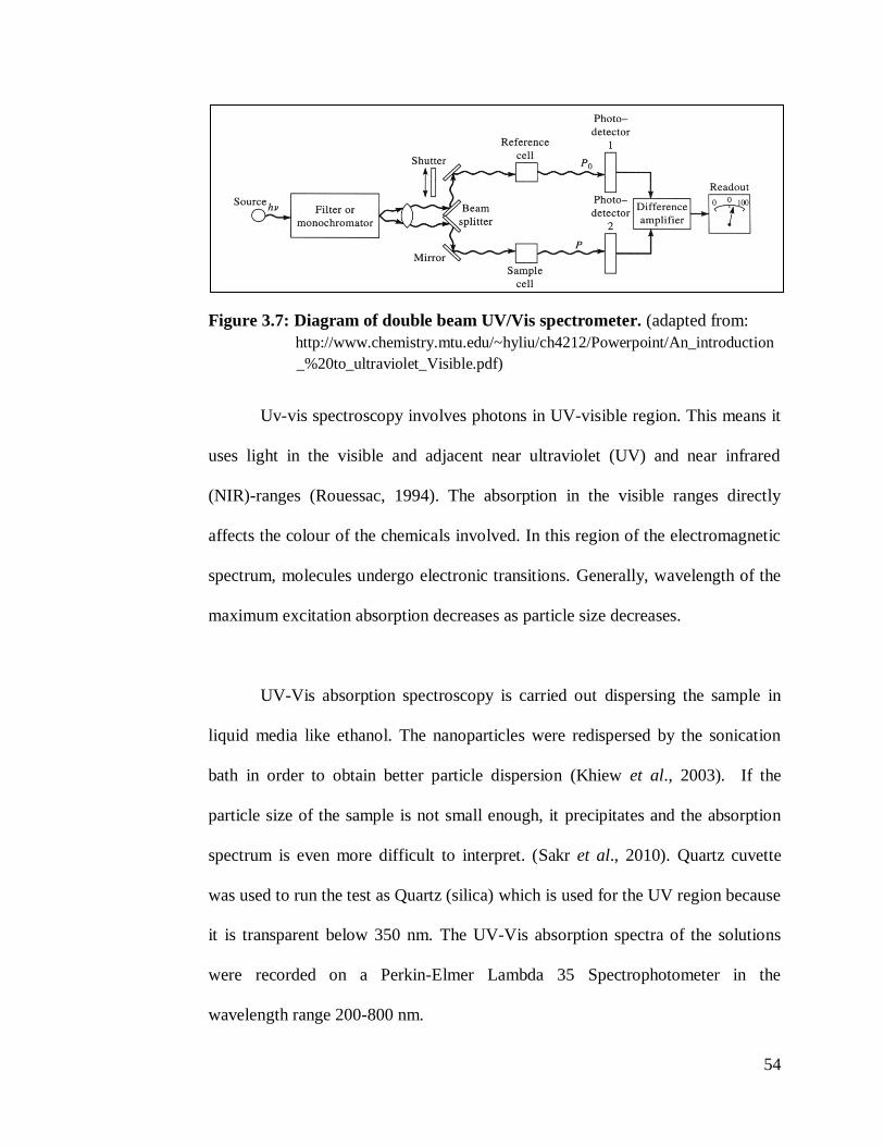
spectrometer. Figure 3.6 shows the diagram of double beam UV/Vis spectrometer.
The UV-Vis absorption spectroscopy is frequently used to characterise
semiconductors thin films and to determine the band gap of the nanostructure
CuSe and also to understand the quantum confinement of the CuSe. The most
dramatic property of semiconductor nanoparticles is the size evolution of the
optical absorption spectra. Hence UV-visible absorption spectroscopy is an
efficient technique to monitor the optical properties of quantum-sized particles
(Pradeep, 2008). Figure 3.7 shows that diagram of double beam UV/Vis
spectrometer.
54
Figure 3.7: Diagram of double beam UV/Vis spectrometer. (adapted from:
http://www.chemistry.mtu.edu/~hyliu/ch4212/Powerpoint/An_introduction
_%20to_ultraviolet_Visible.pdf)
Uv-vis spectroscopy involves photons in UV-visible region. This means it
uses light in the visible and adjacent near ultraviolet (UV) and near infrared
(NIR)-ranges (Rouessac, 1994). The absorption in the visible ranges directly
affects the colour of the chemicals involved. In this region of the electromagnetic
spectrum, molecules undergo electronic transitions. Generally, wavelength of the
maximum excitation absorption decreases as particle size decreases.
UV-Vis absorption spectroscopy is carried out dispersing the sample in
liquid media like ethanol. The nanoparticles were redispersed by the sonication
bath in order to obtain better particle dispersion (Khiew et al., 2003). If the
particle size of the sample is not small enough, it precipitates and the absorption
spectrum is even more difficult to interpret. (Sakr et al., 2010). Quartz cuvette
was used to run the test as Quartz (silica) which is used for the UV region because
it is transparent below 350 nm. The UV-Vis absorption spectra of the solutions
were recorded on a Perkin-Elmer Lambda 35 Spectrophotometer in the
wavelength range 200-800 nm.

55
3.4.3 Photoluminescence (PL) Spectrophotometer
Figure 3.8: Fluorescence Spectrophotometer, Perkin Elmer Precisely LS 55
The characterisation of photoluminescence property of CuSe was done by
using Perkin Elmer LS 55 Fluorescene Spectrometer. Fluorescence
spectrophotometer is an instrument that used to test the photoluminescence (PL)
of a compound. The PL is an important technique used to measure the purity and
optical properties of semiconductors.
PL is a process where an absorbed photon (electromagnetic radiation) at
higher level energy states in a substance after excitation returned back to the
lower energy state by releasing a photon. Electron de-excitation occurs almost
spontaneously and in which emission from a luminescent substance stops when
the exciting source is removed. As a molecule is excited to an electronic state of
E1 from its ground state, E0, the excess energy is removed through fluorescence
emission. Fluorecence occurs from the lowest vibrational level of E1 to various
vibrational levels of E0 and at a longer wavelength than the radiation that caused
the excitation which has shown in Figure 3.9.

56
Figure 3.9: Energy level diagram of fluorescence occurrence. (adapted from:
http://web.njit.edu/~gary/321/Lecture5.html)
As in my research, the sample to be analysed must do some preparations
to obtain a well disperse CuSe solution due to the nanoparticles easily settled
down. Therefore, a very little powder was transferred into a sample vial since the
fluorescence spectrophotometer is very sensitive to concentration and any over
shoot peaks will not able to interpret. Then, a few drop of toluene was poured
inside the sample vial and these steps were repeated for the following samples.
After this, the sample vial was ultrasonicated in a sonicator to finely disperse the
nanoparticles. Finally, the solution was transferred into a Quatz cell cuvette and
placed it into fluorescence spectrophotometer analysis. Unlike UV-Vis
Spectrophotometer, this spectrophotometer does not require the use of reference
cell. The sample was placed in the quartz cell, where it should not exceed the
three quarter level of the cell. The photoluminescence analysis of CuSe in toluene
solution were carried out under the following parameters whereby, Xe lamp was
used, both excitations and emission slits were set at 15 nm, scan speed 500
nm/min and the excitation wavelength was varied from 200 to 300 nm, 10 nm
intervals at 27oC.
0
43210
E1
E0

57
CHAPTER 4
RESULTS AND DISCUSSION
4.1 Results
In this experiment, the formation of micelles system is involved in the
synthesis of copper selenide nanoparticles. Upon mixing all of the solution, a dark
brown colour solution appeared which indicates that the presence of selenide
source have been reduced to Se2-
. The solution contains the surfactant molecules,
CTAB, acting as the stabiliser for the emulsion system. During the reaction, the
mixture was stirred vigorously by using hot-plate to ensure a completed reaction
and to stabilise the emulsion system. With stirring, the stability of the emulsion
system can be maintained and agglomeration of particles can be prevented.
The surfactant employed in this experiment is CTAB, a cationic surfactant
whose hydrophilic headgroup carries a net positive charge. The presence of
surfactant will affect the growth and particles characteristics significantly. It is
very important in the particle formation due to its ability for compartmentalisation.
The positively charged headgroups can easily attach the metal clusters‟ surface to
make them soluble in the water environment; the cetyl hydrophobic chain is
toward to oil phase.

58
Apart from surfactant, another material used in this synthesis is sodium
borohydride, NaBH4. It is a strong soluble hydride reducing agent, and is capable
in reducing the Na2SeO3 source to Se2-
. The reducing agent was added to the
solution under stirring condition about 30 minutes. The formation of micelle
system in synthesis of copper selenide nanoparticles is illustrated in Figure 4.1.
Cu2+
H33C16
CH3CH3CH3
N+
Br-
NaBH4
water phase
+
Se2-
Se2-
Se2-
Se2-
Se2-
Se2-
Se2-
Se2-
Se2-
Se2-
Cu2+
Cu2+
Cu2+
Cu2+
Cu2+
Cu2+
Cu2+
Cu2+
Cu2+
Cu2+
Hydropil ic headHydrophobic tai l
Oil phase
Na2SeO3 + Se2-
Br-
Br- Br
-
Br-Br
-
Br-
Br-
Br-
Br-
Br-
+
+
+
+
+
+
+
+
+
+
Figure 4.1: Formation of micelle system in synthesis of copper selenide
nanoparticles.

59
In this research, the samples of copper selenide nanoparticles synthesised
in different parameters were characterised by using X-ray Diffractometer, UV-Vis
(UV-Vis) Spectrophotometer and Photoluminescence (PL) Spectrophotometer.
These characterisations were carried out under room temperature condition.
4.1.1 X-Ray Diffractometer (XRD)
The seven samples synthesised in different parameters of various
concentrations of reducing agent, [NaBH4], effect of stirring period and effect of
autoclave period were characterised by using X-ray Diffractometer and the results
obtained are shown in Figure 4.2 - 4.4, respectively. Meanwhile, the matching of
the 2θ and d-spacing values for each peaks of the samples with JCPDS No. 00-
020-1020 corresponding to the hexagonal phase CuSe. The summaries of these
matching of the 2θ and d-spacing values for each peaks of the sample are shown
in Table 4.1 - 4.3, respectively.

60
Figure 4.2: XRD pattern of samples prepared at various reducing
agent concentration, [NaBH4]
20 30 40 50 60
(116)(101)
(103)
S3030[3.0 M]
S3025[2.5 M]
S3020[2.0 M]
(201)(108)
(110)
(106)(006)
(102)
2 (Degree)
Inte
nsity (
arb
itary
unit)

yyu
Table 4.1: XRD data for sample prepared at various reducing agent concentration
Sample
Code
2θ (o) d-
spacing
(Å)
2θ (o) d-
spacing
(Å)
2θ (o) d-
spacing
(Å)
2θ (o) d-
spacing
(Å)
2θ (o) d-
spacing
(Å)
2θ (o) d-
spacing
(Å)
2θ (o) d-
spacing
(Å)
JCPDS
No. 00-
020-
1020
46.08 1.968 31.14 2.870 28.12 3.170 30.49 2.929 40.93 2.203 50.08 1.820 54.09 1.694
S3020 45.43 1.995 31.10 2.873 27.98 3.186 30.04 2.972 40.86 2.206 49.86 1.828 53.65 1.707
S3025 45.26 2.002 30.98 2.884 27.88 3.198 30.98 2.884 40.71 2.215 48.86 1.828 53.41 1.714
S3030 44.97 2.014 31.18 2.866 27.96 3.188 30.20 2.957 40.96 2.201 50.04 1.821 53.26 1.718
(hkl) 110 006 102 103 106 108 201
Unit
cell
Hexagonal
61

62
Figure 4.3: XRD pattern of samples prepared at various
periods(under stirring condition)
20 30 40 50 60
(101)
(201)
(108)
(110)
(106)(006)
(103)
(102)
S302033 hours
S302022 hours
S30201 hour
2 Degree
Inte
nsity a
rbitary
(unit)

63
95
yyu
Table 4.2: XRD data for sample prepared at various stirring period
Sample
Code
2θ (o) d-
spacing
(Å)
2θ (o) d-
spacing
(Å)
2θ (o) d-
spacing
(Å)
2θ (o) d-
spacing
(Å)
2θ (o) d-
spacing
(Å)
2θ (o) d-
spacing
(Å)
2θ (o) d-
spacing
(Å)
JCPDS
No. 00-
020-
1020
46.08 1.968 31.14 2.870 28.12 3.170 30.49 2.929 40.93 2.203 50.08 1.820 54.09 1.694
S3020 45.43 1.995 31.10 2.873 27.98 3.186 30.04 2.972 40.86 2.206 49.86 1.828 53.65 1.707
S30202 45.49 1.992 31.20 2.864 28.00 3.184 30.40 2.938 40.91 2.204 50.08 1.820 53.63 1.708
S30203 45.20 2.004 31.18 2.866 28.08 3.175 30.44 2.934 40.62 2.219 50.09 1.820 53.49 1.712
(hkl) 110 006 102 103 106 108 201
Unit
cell
Hexagonal

64
Figure 4.4: XRD pattern of samples prepared at various periods
(under autoclave condition)
20 30 40 50 60
101(116)
(103)
(201)(108)
(110)
(106)(006)
(102)
S902090 minutes
S602060 minutes
S302030 minutes
2 (Degree)
Inte
nsity (
arb
itary
unit)

65
Table 4.3: XRD data for sample prepared at various heated-treatment period
Sample
Code
2θ (o) d-
spacing
(Å)
2θ (o) d-
spacing
(Å)
2θ (o) d-
spacing
(Å)
2θ (o) d-
spacing
(Å)
2θ (o) d-
spacing
(Å)
2θ (o) d-
spacing
(Å)
2θ (o) d-
spacing
(Å)
JCPDS
No. 00-
020-
1020
46.08 1.968 31.14 2.870 28.12 3.170 30.49 2.929 40.93 2.203 50.08 1.820 54.09 1.694
S3020 45.43 1.995 31.10 2.873 27.98 3.186 30.04 2.972 40.86 2.206 49.86 1.828 53.65 1.707
S9020 45.21 2.004 31.16 2.868 27.14 3.283 30.42 2.936 40.66 2.217 49.95 1.824 53.36 1.716
S6020 45.30 2.000 31.20 2.864 27.29 3.265 30.54 2.925 40.72 2.214 50.07 1.820 53.60 1.709
(hkl) 110 006 102 103 106 108 201
Unit
cell
Hexagonal

66
X-Ray diffraction is the principal method used to identify the phase
present in solid-state material. According to the crystallite size that is performed
by measuring the broadening of a particular XRD peaks in a diffraction pattern
associated with a particular planar reflection from within the crystal unit cell.
Thus, if the full width at half maximum (FWHM) of the diffraction angle is given,
the mean crystallite sizes of the samples can be calculated through Debye-
Scherrer‟s equation which is shown as below:
Where, D = mean crystallite size perpendicular to normal line of (hkl)
plane
K = constant equal to 0.9
λ = the X-Ray wavelength, 1.5419Å
β = FWHM of the (hkl) diffraction peak in radian
θ = Bragg angle of the (hkl) diffraction peak
By using Debye-Scherrer‟s equation, the main XRD peaks of plane (110) were
chosen to calculate the mean crystallite size in order to minimise errors. The mean
crystallite size calculated for the selected samples were shown in Table 4.4.

67
Table 4.4: Comparison of mean crystallite size for seven samples
Sample
code
FWHM in
2θ (o)
β calculated
from
FWHM in
radian
2θ of (110)
peak (o)
θ of (110)
peak (o)
Calculated
mean
crystallite
size (nm)
S3020 1.0709 0.0187 45.4245 22.7123 8.0447
S3025 0.9943 0.0174 45.2582 22.6291 8.6405
S3030 0.4236 0.0074 44.9708 22.4854 20.2958
S6020 0.8855 0.0155 45.2062 22.6031 9.6979
S9020 0.6247 0.0109 45.3018 22.6509 13.7953
S30202 1.2762 0.0223 45.4928 22.7464 6.7477
S30203 0.5580 0.0097 45.2033 22.6017 15.4964
(Note: The calculation and graph of comparison between mean crystallite size
versus each parameter used are shown in Appendix B)
The XRD patterns for all the CuSe samples of are shown in Figure 4.2 -
4.4, respectively. From the three Figures which show that there are nine peaks
appeared in the spectrum. The 2θ and d-spacing values of these peaks given by
the diffraction patterns were matched with the standard database values of JCPDS
card No. 00-020-1020 which has been summarised in Table 4.1 - 4.3, respectively.
From these Figures, the diffraction patterns of three predominant peaks were
exhibited at about 46.00, 31.00 and 28.00 degrees, which were indexed to
scattering from the (110), (006) and (102) planes of hexagonal phase CuSe.
Therefore, the hexagonal phase CuSe had been considered successfully
synthesised by adding reducing agent, increasing period of stirring and heated-
treatment.

68
The reducing agent, NaBH4 was introduced in synthesising of copper
selenide nanoparticles. It will reduce the selenite ions (SeO32-
) to selenide ions
(Se2-
). The chemical reaction can be formulated as follows:
NaBH4 (aq) Na+
BH4
-(aq) (aq)+
BH4
-(aq) SeO3
2-HSe
-B(OH)3(aq) (aq) (aq)+ +
2 HSe-
Cu2+
2 CuSe
(aq)
(aq) (s)
(g)+
+
2 OH-
(aq)+ 2 H2OSe2- (aq)
Se2-
(aq)
(Ambade et al., 2006)
From the above reaction equation, it shows that sodium selenite, Na2SeO3
released higher concentration of Se2-
in the presence of reducing agent. Then, Se2-
source only can react with the Cu2+
solution to form CuSe nanostructure. In
addition, the mean crystallite size was increased by increasing the reducing agent
as this will facilitate the growth of nanoparticles under non-equilibrium kinetic
growth conditions. To conclude, NaBH4 favors the formation of copper selenide
nanostructure.
Figure 4.3 shows XRD pattern of samples prepared at various periods
under stirring condition. The spectrum shows that the peaks were observed to be
higher intensity by increasing the period of stirring. Meanwhile, the calculated
mean crystallite size was in between 8.0447 – 15.4964 nm while prolonging the
period of stirring. This is due to molecules are well mixed which lead to have a

69
greater chance of colliding, therefore, prolong the stirring period will lead to
higher opportunity of collision between the particles and then to form a larger size
of the particles. The collision was accelerated under stirring condition.
From Figure 4.4 shows XRD pattern of samples prepared at various
heated-treatment periods. The spectrum shows that the peaks were observed to be
more intense and narrower by increasing the heated-treatment of reaction time. In
addition, the mean crystallite size was increased by increasing the heated-
treatment period which is shown in Table 4.4. This is because the reactants can
react with each other within a short time. This leads to an increase in the reaction
rate and the sizes of the particles increased with increasing in reaction duration,
thereby reducing the required reaction durations.
Based on the above observation, one can conclude that small diameter
nanoparticles formed at lower concentration of the reducing agent, shorter period
of stirring and shorter heated-treatment reaction time. In the meantime, further
characterization like transmission electron microscopy (TEM) or scanning
electron microscopy (SEM) are needed in order to confirm the size and
morphology of the synthesised CuSe.

70
4.1.2 UV/Vis Spectrophotometer (Optical properties)
All the seven samples synthesised in different parameters were
characterised by using UV-Vis Spectrophotometer and the results obtained are
shown in Figure 4.5 - 4.7, respectively. Optical properties, which are directly
related to the size of nanoparticles, can be studied using the absorption spectra of
CuSe.
Figure 4.5: UV/Vis absorption spectrum of CuSe nanoparticles at
different concentration of reducing agent S3020 = 2.0 M,
S3025 = 2.5 M, S3030 = 3.0 M, respectively.
0
1
2
400 500 600 700 800
S3030[3.0 M]
S30252.5 M]
S3020[2.0 M]
Wavelength (nm)
Absorb
ance

71
Figure 4.6: UV/Vis absorption of CuSe nanoparticles prepared at
different period (under stirring condition) S3020 = 1 hour,
S30202 = 2 hours, and S30203 = 3hours, respectively.
0
0.5
1.0
1.5
2.0
400 500 600 700 800
S302033 hours
S302022 hours
S30201 hour
Wavelength (nm)
Absorb
ance

72
Figure 4.7: UV/Vis absorption of CuSe nanoparticles prepared at
different autoclaved period S3020 = 30 minutes,
S6020 = 60 minutes, and S9020 = 90 minutes.
Form Figures 4.5 - 4.7 show that the absorption onset wavelength for all
the samples approximately 487 nm and they are blue shift. The band gap energy
for bulk CuSe is equal to 1.3 eV (Seoudi et al., 2006).
0
0.5
1.0
1.5
400 500 600 700 800
S902090 mins
S602060 minsS302030 mins
Wavelength (nm)
Absorb
ance

73
From the figures, it can be observed that the absorption edge move to the
blue shift which shift to the shorter wavelength. Therefore, it indicates that
decrease in the particle size. This blue shift is due to the quantum confinement
effect (Seoudi et al., 2006). It could be concluded that the changes concentration
of reducing agent, time of stirring rate and heated-treatment period will have
effect on the particle size. This is probably due to the increase of formation rate of
nuclei and growth rate of copper selenide nanoparticles. Hence, increasing one of
the above effects will lead to the higher nucleation rate of copper selenide
nanoparticles formed and growing larger through particle-particle aggregation.
The theory of optical absorption gives the relation between the absorption
coefficient and the photon energy, for direct allowed transition as:
Where A is the constant, Eg is the band gap, hv is the photon energy and n is the
exponent which determine the type of the electronic transition causing absorption.
The value taken for direct forbidden is ½ (Ambade et al., 2006). The relation
between (αhv)2 against hv for the seven samples are shown in Figure 4.8 - 4.10,
respectively. The value of absorption coefficient (α) is calculated from the
relation
where A is absorption of the sample in UV and t is thickness of the cuvette.

74
a.) Relation between (αhv)2 and photon energy (hv) for S3020
b.) Relation between (αhv)2 and photon energy (hv) for S3025
0
50
100
150
1.0 1.2 1.4 1.6 1.8 2.0 2.2 2.4 2.6 2.8 3.0 3.2 3.4 3.6 3.8 4.0
2.4 eV
hv (eV)
(hv
)2 (eV
-2 c
m-2
)
S3020
0
50
100
150
1.0 1.2 1.4 1.6 1.8 2.0 2.2 2.4 2.6 2.8 3.0 3.2 3.4 3.6 3.8 4.0 4.2 4.42.24 eV
hv (eV)
(hv)2
(eV
-2 c
m-2
)
S3025

75
c.) Relation between (αhv)2 and photon energy (hv) for S3030
Figure 4.8: Relation between (αhv)2 and photon energy (hv) for CuSe
nanoparticle prepared at various reducing agent, NaBH4.
S3020 = 2.0 M, S3025 = 2.5 M and S3030 = 3.0 M
0
50
100
150
1.0 1.2 1.4 1.6 1.8 2.0 2.2 2.4 2.61.97 eV
hv (eV)
(hv)2
(eV
-2 c
m-2
)
S3030

76
a.) Relation between (αhv)2 and photon energy (hv) for S30202
b.) Relation between (αhv)2 and photon energy (hv) for S30203
Figure 4.9: Relation between (αhv)2 and photon energy (hv) for CuSe
nanoparticle prepared at various time of stirring.
S3020 = 1 h, S30202 = 2 h and S30203 = 3h
0
60
120
180
1.0 1.2 1.4 1.6 1.8 2.0 2.2 2.4 2.6 2.8 3.0 3.2 3.42.03 eV
hv (eV)
(hv
)2 (
eV -2
cm-2
)
S30202
0
50
100
150
1.0 1.2 1.4 1.6 1.8 2.0 2.2 2.4 2.6 2.8 3.0 3.2 3.4 3.6 3.8 4.0
1.87 eV
hv (eV)
(hv
)2 (eV
-2cm
-2)
S30203

77
a.) Relation between (αhv)2 and photon energy (hv) for S6020
b.) Relation between (αhv)2 and photon energy (hv) for S3020
Figure 4.10: Relation between (αhv)2 and photon energy (hv) for CuSe
nanoparticle prepared at various time of stirring.
S3020 = 30 mins, S6020 = 60mins and S9020 = 90 mins
0
60
120
180
1.0 1.2 1.4 1.6 1.8 2.0 2.2 2.4 2.6 2.8 3.0 3.2 3.4 3.6 3.8 4.01.87 eV
hv (eV)
(hv
)2 (eV
-2 c
m-2
)
S6020
0
50
100
150
1.0 1.2 1.4 1.6 1.8 2.0 2.2 2.4 2.6 2.8 3.0 3.2 3.4 3.6 3.8 4.01.87 eV
hv (eV)
(hv
)2 (eV
-2 c
m-2
)
S9020

78
From Figure 4.8 - 4.10, it can be observed that the optical band gap energy
can be determined by extrapolating the curve to the energy axis for zero
absorption coefficients. The optical band gap energies of CuSe nanoparticles have
been estimated to be in the range of 1.87 – 2.40 eV which is direct band gap. The
literature value for bulk CuSe is 1.30 eV (Seoudi, 2006). The comparison of the
band gap value between samples values and literature band gap value are shown
as below:
Table 4.5: Comparison of band gap energy values of samples prepared and
literature band gap energy values.
Sample code Band gap energy
(eV)
Literature band
gap energy (eV)
S3020 2.24 1.30
S3025 1.97 1.30
S3030 2.40 1.30
S6020 2.03 1.30
S9020 1.87 1.30
S30202 2.03 1.30
S30203 1.87 1.30
From the Table 4.5, it shows that optical band gap energy is inversely
proportional to the crystallize size. Therefore, by increasing the concentration of
reducing agent, stirring time and heated-treatment period will have effect on the
band gap energy.

79
4.1.3 Photoluminescence (PL) Spectrophotometer
Figure 4.11 shows the control set that was run before the samples in order
to ensure that the obtained emission peak did not originate from the solvent
involved in the reaction. The control set (reference) is toluene.
The seven samples prepared at different parameters were characterised by
photoluminescence spectrophotometer and the results achieved are shown in
Figure 4.12 - 4.14, respectively.
Table 4.6: Summary of the emission peak and fluorescence intensity for all
samples prepared in different parameters.
Samples code Emission peak /nm Fluorescence Intensity
(FI)
S3020 438 572
S3025 438 575
S3030 438 575
S30202 438 572
S30203 438 572
S6020 438 574
S9020 438 574

80
Figure 4.11: Photoluminescence spectrum of control set for the
synthesis of copper selenide.
Figure 4.12: PL spectra of all the CuSe samples prepared at different
concentration of reducing agent used.
0
200
400
600
800
200 300 400 500 600
578
296
Wavelength (nm)
Inte
nsi
ty (
a.
u)
0
200
400
600
800
400 450 500 550 600
575S3030
S3025
S3020
413
438
Wavelength (nm)
Inte
nsi
ty (
a.u
)

81
Figure 4.13: PL spectra of all the CuSe samples prepared at
different stirring period.
Figure 4.14: PL spectra of all the CuSe samples prepared at different
heated-treatment period.
0
200
400
600
800
400 450 500 550 600
572
413
438
S30203
S3020
S30202
Wavelength (nm)
Inte
nsity (
a.u
)
0
200
400
600
800
400 450 500 550 600
574
413
438
S9020
S6020
S3020
Wavelength (nm)
Inte
nsi
ty (
a.u
)

82
From the overlay absorption spectrum obtained throughout the Figure 4.12
- 4.14, all the seven samples showed an emission peak at around 438 nm. As
compared to the control set spectrum (Figure 4.11), it can be seen that there is no
significant emission peak at around 438 nm. The emission peak and fluorescence
intensity for each sample is summarised in the Table 4.6. There is no obvious
relationship between 3 parameters used and the emission peak of the sample.
All the seven samples showed a fluorescence emission peak at around 438
nm which belonged to the blue luminescence. The luminescence of copper can be
brought about by exciting the sample with electrons, photons, or laser beams.
With different synthetic method or surfactant employed, the emission peak
positions can be distributed in the region of 320 – 520 nm. The
photoluminescence property of copper selenide nanoparticles is depended on the
size where its emission will shift to higher energy with decreasing the particles
size. As the emission intensity and position is both dependant on the absorption of
light source by the samples.
The fluorescence intensity of a sample is related to the quantum yield
where the number of photons emitted is divided by the number of photons
absorbed. Higher quantum yield would produce higher intensity and vice versa. In
this experiment, the fluorescence intensities for all the seven samples are
relatively high. The high quantum yield may be the reason of the visible

83
photoluminescence property was observed when the samples were examined
under UV lamp. This may due to the particles that are formed using this
concentration is the most in particle quantity. As a result, more particles will
absorb the light source and emit it as fluorescence.

84
CHAPTER 5
CONCLUSION
CuSe nanoparticles had been successfully synthesised using ternary oil in
water (o/w) emulsion technique.
All of the samples were found to be existed in hexagonal phase. By
increasing the concentration of reducing agent, stirring period and heated-
treatment period, the mean crystallite size will be increased which varied between
1.87 – 2.40 nm. Due to this reason, the band gap energy was decreased. This is
because the mean crystallite size is inversely proportional to the optical band gap
energy of the compound. The optical band gap energies of CuSe nanoparticles in
this research have been estimated to be in the range of 1.87 – 2.40 eV which is a
direct band gap.
An emission peak was observed in the visible range at about 438 nm when
the samples had been examined by Photoluminescence (PL) Spectrophotometer.
PL peaks of CuSe were blue shift to the UV region due to the decrease in particles
sizes led to increase band gap values correspondingly. The trend of the peaks
decreased with increasing excitation wavelength also due to the PL were size-

85
dependent to the particles so more energy was needed in order to excite one
electron from the valence band to conduction band.
In the future work, it is suggested using different of temperature, pressure,
ageing time of emulsion, water to cyclohexane and reactants ratio, type of
surfactant, and co-surfactant could be used in order to obtain different emulsion
system. Therefore, the morphology of CuSe could be varied. Transmission
electron microscopy (TEM) or scanning electron microscopy (SEM) should be
carried out to check on the morphology and the size of the compound.

86
BIBLIOGRAPHY
Journal:
Ago, H., Abe, H. and Shimizu, T. (2006). Experimental study on thermal
characteristics of suspended platinum nanofilm sensors. International
Journal of Heat and Mass Transfer, 49, 3879–3883
Ambade, S. B., Mane, R. S., Kale, S. S., Sonawane, S. H., Tokle, T. and
McClements D. J. (2010). Physicochemical properties of lactoferrin
stabilized oil-in-water emulsions:Effects of pH, salt and heating. Journal
of Food Hydrocolloids, 25, 976-982
Asiyanbola, B. and Soboyejo, W. (2008). For the Surgeon: An Introduction to
Nanotechnology. Journal of Surgical Education, 8, 137 - 144
Bera, D., Qian, L., Tseng T. K. and Holloway, P. H. (2010). Quantum Dots and
Their Multimodal Applications: A Review. Materials, 3, 2260-2345
Bhattacharya, R. and Saha, S. (2008). Growth of CdS nanoparticles by chemical
method and its characterization. Journal of physics @ Indian Academy of
Sciences, 71, 187-192.
Capek (2004). Preparation of metal nanoparticle in water-in-oil (w/o)
microemulsion. Journal of Advances in Colloid and Interface Science, 110,
49-74.

87
Gosavi, S. R., Deshpande, N. G., Gudagea, Y. G. and Sharma, R. (2007). Physical,
optical and electrical properties of copper selenide (CuSe) thin films
deposited by solution growth technique at room temperature. Journal of
Alloys and Compounds,448, 344–348
Eastoe, J. Martin, J. H. and Maura H. (2006). Recent advances in Nanoparticle
synthesis with reversed micelles. Journal of colloid and interface science,
259, 277-281
Khiew P. S., Radiman, S., Huang, N. M. and Ahmad, M. S. (2003). Studies on the
growth and characterisation of CdS and PbS nanoparticles using sugar-
ester non-ionic water-in-oil microemulsion. Journal of crystal Growth 254,
235-243
Kumar, P., Singh, K. and Srivastava O. N. (2010). Template free-solvothermaly
synthesised copper selenide (CuSe, Cu2_xSe, β-Cu2Se & Cu2Se)
hexagonal nanoplates from different precursors at low temperature,
Journal of Crystal Growth, 312, 2804–2813
Kung, H. H. and Kung, M. C. (2004). Nanotechnology: applications and
potentials for heterogeneous catalysis. Journal of Catalysis Today, 97
219–224
Liu, J. C., Ikushima, Y. and Shervani Z. (2003). Environmentally benign
preparation of metal nano-particles by using water-in-CO2 microemulsions
technology. Journal of Current Opinion in Solid State and Materials
Science, 7, 255–261
Lopez-Quintela, M. A. (2003). Synthesis of nanomaterials in microemulsions:
formation mechanisms and growth control. Current Opinion in Colloid
and Interface Science, 8, 137 - 144

88
Lu, C. H., Lee, C. H. and Wu, C. H. (2010). Microemulsion-mediated
solvothermal synthesis of copper indium diselenide powders. Journal of
Solar Energy Materials & Solar Cells, 94, 1622–1626
Mangalaraj, D., and Narayandass, S. K (2006). The effect of annealing on
vacuum-evaporated copper selenide and indium telluride thin films.
Materials Characterization, 58, 756–764
Ohtsuki K.(2000). Evaluation of collision and stirring rates in circumplanetary
particle disks based on three-body orbital integrations. Current Opinion in
Colloid and Interface Science, 8, 128
Peranantham, P., Jeyachandran, Y. L., Viswanathan, C., Praveena, N. N., Chitra,
P. C., Hankare, P. P., Khomane, A. S., Chate, P. A., Rathod, K. C. and
Garadkar, K. M. (2008). Preparation of copper selenide thin films by
simple chemical route at low temperature and their characterization.
Journal of Alloys and Compounds, 469, 478–482
Sakr, G. B., Yahia, I. S., Fadel M., Fouad, S. S. and Romcevic N. (2010). Optical
spectroscopy, optical conductivity, dielectric properties and new methods
for determining the gap states of CuSe thin films. Journal of Alloys and
Compounds, 507, 557–562
Seoudi, R., Shabaka, A.A., Elokr, M.M., Seoudi, A. S. R., Shabaka, A. A. and
Sobhi, A. (2006). Optical properties and electrical conductivity studies of
copper selenide nanoparticle. Journal of Materials Letters, 61, 3451–3455
Shaikh, A. V. and Han, S. H. (2006). Chemical synthesis of p-type
nanocrystalline copper selenide thin films for heterojunction solar cells.
Journal of Applied Surface Science, 253, 2123–2126

89
Vinod, T. P., Jin, X. and Kim J. K. (2010). Hexagonal nanoplatelets of CuSe
synthesized through facile solution phase reaction. Materials Research
Bulletin, 46, 340 – 344
Wang, C. C., Chen, A. L. and Chen, I. H. (2006). Effect of chelating functional
polymer on the size of CdS nanocluster formation. Journal of Colloid and
Interface Science, 293, 421–429
Wei, W., Zhang, S. Y., Fang, C. X., Zhao S. Q., Jin, B. K., Zhang, X., Xie, H. Q.,
Fujii, M., Takahashi, K., Ikuta, T., Li, Y. Z., Gao X. D., Yang, C. and
Huang F. Q. (2010).The effects of sputtering power on optical and
electrical properties of copper selenide thin films deposited by magnetron
sputtering. Journal of Alloys and Compounds, 505, 623–627
Wu, J. and Tian, Y. (2007). Electrochemical behavior and electrogenerated
chemiluminescence of crystalline CuSe nanotubes. Journal of Solid State
Sciences, 10, 622-628
Xu, J. and Li, Y. (2003). Formation of zinc sulfide nanorods and nanoparticles in
ternary W?O microemulsion. Journal of colloid and interface sciences,
259, 275-281
Zhang, X., Xie, H. Q., Fujii, M., Takahashi, K., Ikuta, T., Ago, H., Abe, H. and
Shimizu, T. (2006). Experimental study on thermal characteristics of
suspended platinum nanofilm sensors. International Journal of Heat and
Mass Transfer, 49, 3879–3883
Zainal, Z., Nagalingam, S. and Tan, C. L. (2005). Copper selenide thin films
prepared using combination of chemical precipitation and dip coating
method. Materials Letter, 59, 1391 - 1394

90
Books:
Atkins, P. and Paula, J. D. (2006). Atkins‟ Physical Chemistry. 8th Edition. (pp
690 – 728). New York: Oxford.
Dann, S. (2002). Reaction and Characterization of Solids. 1st Edition. p. 55-57.
New York: John Wiley & Sons, Inc.
Dutta, P. and Gupta, S. (2008). Understanding of Nano Science and technology,
1st Edition. p. 1-2. New Delhi: Global Vision Publishing House.
Hammond, C. (2009). The basics of crystallography and diffraction 3rd
Edition.
(pg 196-198). New York: Oxford University Press Inc.
Housecroft, C. E. and Sharpe, A. G. (2008). Inorganic Chemistry. 3rd
Edition. P.
167. Pearson Education, Inc.
Ian D. M. and Ross, S. (2002). Colloidal Dispersions Suspensions, Emulsions,
and Foams. Wiley-Interscience: John Wiley & Sons, Ltd.
Kelsall, Robert W., Hamley, Ian W., and Geoghegam, M. (2005).
Nanotechnology: Nanoscale science and technology. (pp 1-5, 131-135,
259). West Sussex: John Wiley & Sons, Ltd.
Manasi K. (2008). Nanotechnology: Fundamental and Application (pp 14, 51-58).
New Dehli: I.K International Publishing House Pvt. Ltd.
Pradeep, T (2008). Nano: The Essentials understanding anoscience and
nanotechnology. (pp 75-81, 123-125, 186-196, 307-309). 7 West Patel
Nagar, New Delhi: Tata McGraw-Hill Publisher.

91
Ratner, M. and Ratner, D. (2003). Nanotechnology: A gentle Introduction to The
Next big Idea (pp 6-7). Pearson Education, Inc.
Rouessac, F. and Rouessac, A. (1994). Chemical Analysis: Modern
Instrumentation Methods and Techniques (pp 167-173) John Wiley &
Sons, Ltd.
Silberberg, M. S. (2009). Chemistry The Molecular nature of Matter and Change.
5th Edition. (pp 489 – 491). New York:McCraw-Hill companies, Inc.
Smart, L. and Moore, E. (2005). Solid State Chemistry: An Introduction. 3rd
Edition. (pp 27, 77-82, 89). United States: Taylor & Francis Group, LLC.
Websites:
A schematic diagram of a powder diffractometer. URL:
http://chemwiki,ucdavis.edu/analytical_chemistry/instrumental_analysis/p
owder_x-ray_diffraction. Accessed on 6st November 2010.
Colloidal quantum dots irradiated with a UV light. Different sized quantum dots
emit different color light due to quantum confinement. URL:
http://www.mdpi.com/1996-1944/3/4/2260/pdf. Accessed on 1 July 2010.
Applications of Nanotechnology. URL:
http://www.nanowerk.com/nanotechnology/introduction/introduction_to_n
anotechnology_12.php
Comparison of emulsion and microemulsion. URL:
http://www.pharmainfo.net/reviews/microemulsions-novel-drug-delivery-
vehicle. Accessed on 7 July 2010.
CuSe and Its application. Retrieved from Principles of Semiconductor Devices
URL:
http://www.nanowerk.com/nanotechnology/introduction/introduction_to_n
anotechnology_7.php. Accessed on 6 July 2010.

92
Diagram of double beam UV/Vis spectrometer. URL:
http://www.chemistry.mtu.edu/~hyliu/ch4212/Powerpoint/An_introductio
n_%20to_ultraviolet_Visible.pdf. Accessed on 23 July2010.
E-k diagram illustrating
a) Photon absorption in a direct band gap semiconductor
b) Photon absorption in an indirect band gap semiconductor assisted by
phonon absorption and
c) Photon absorption in an indirect band gap semiconductor assisted by
phonon emission. URL:
http://ecee.colorado.edu/~bart/book/book/chapter4/ch4_6.htm. Accessed
on 23 December 2010.
Energy level diagram of fluorescence occurrence. URL:
http://web.njit.edu/~gary/321/Lecture5.html. Accessed on 23 July2010.
Nanomaterial. URL: http://www.scribd.com/doc/13787393/Nano-Materials.
Accessed on 23 July2010.
Nanotechnology: The New Era of Science. URL:
http://www.docstoc.com/docs/39210887/Nanotechnology-The-New-Era-
of-Science-F. Accessed on 27 August 2010.
Molecular structures of a single-walled carbon nanotube (SWNT) and of a multi-
walled carbon nanotube (MWNT). URL:
http://www-ibmc.ustrasbg.fr/ict/vectorisation/nanotubes_eng.shtml.
Accessed on 27 August 2010.
Schematic representation of the building up of Nanostructures. URL:
http://www.gitam.edu/eresource/nano/nanotechnology/role_of_bottomup_
and_topdown_a.htm. Accessed on 1st November 2010.
The band diagram for nano-sized crystals of semiconductor (quantum dots). URL:
http://www3.imperial.ac.uk/. Accessed on 23 December 2010.
The comparison of size with different matters. URL:
http://nanoscience.massey.ac.nz/. Accessed on 2 July 2010.

93
APPENDICIES
APPENDIX A
Example Calculation for the mole and mass of CTAB,
Example Calculation for the mole and mass of CuCl2∙2H2O,
2 2

94
Example Calculation for the mole and mass of Na2SeO3,
Na2 O3
Example Calculation for the mole and mass of NaBH4,
Note: The mole and concentration of the CTAB, CuCl2∙2H2O, NaSe2O3 and
NaBH4 used were calculated for each parameters and tabulated as below:-

63
95
yyu
Preparation of samples at various concentration of reducing agent (NaBH4)
Preparation of samples at different time of stirring
Sample DI H2O
(mL)
Cyclohexane
(mL)
CTAB Cu2+
Se2-
Time
of stirring Autoclave
Conc. of NaBH4
(mol dm-3
) Conc.
(mol dm-3
) Mole
Conc.
(mol dm-3
)
Vol. of DI to
dissolve
(mL)
Mole Conc.
(mol dm-3
)
Vol. of DI to
dissolve
(mL)
Mole
S3020
10 5 0.1 0.001 0.1 50 0.005 0.1 50 0.005 1h 30 mins,
1210c
2.0
S3025
10 5 0.1 0.001 0.1 50 0.005 0.1 50 0.005 1h 60 mins,
1210c
2.5
S3030
10 5 0.1 0.001 0.1 50 0.005 0.1 50 0.005 1h 90 mins,
1210c
3.0
Sample DI H2O
(mL)
Cyclohexane
(mL)
CTAB Cu2+
Se2-
Time
of stirring Autoclave
Conc. of NaBH4
(mol dm-3
) Conc.
(mol dm-3
) Mole
Conc.
(mol dm-3
)
Vol. of DI to
dissolve
(mL)
Mole Conc.
(mol dm-3
)
Vol. of DI to
dissolve
(mL)
Mole
S3020
10 5 0.1 0.001 0.1 50 0.005 0.1 50 0.005 1h 30 mins,
1210c
2.0
S30202
10 5 0.1 0.001 0.1 50 0.005 0.1 50 0.005 2h 30 mins,
1210c
2.0
S30203
10 5 0.1 0.001 0.1 50 0.005 0.1 50 0.005 3h 30 mins,
1210c
2.0

96
Preparation of samples at different heated-treatment period
Sample DI H2O
(mL)
Cyclohexane
(mL)
CTAB Cu2+
Se2-
Time
of
stirring
Autoclave Conc. of NaBH4
(mol dm-3
) Conc.
(mol dm-3
) Mole
Conc.
(mol dm-3
)
Vol. of DI to
dissolve
(mL)
Mole Conc.
(mol dm-3
)
Vol. of DI to
dissolve
(mL)
Mole
S3020
10 5 0.1 0.001 0.1 50 0.005 0.1 50 0.005 1h 30 mins,
1210c
2.0
S6020
10 5 0.1 0.001 0.1 50 0.005 0.1 50 0.005 1h 60 mins,
1210c
2.0
S9020
10 5 0.1 0.001 0.1 50 0.005 0.1 50 0.005 1h 90 mins,
1210c
2.0

97
APPENDIX B
The calculated β values and mean crystallite sizes for the selected samples
S3020, S3025 and S3030.
Sample
code
FWHM in
2θ (o)
β calculated
from
FWHM in
radian
2θ of (110)
peak (o)
θ of (110)
peak (o)
Calculated
mean
crystallite
size (nm)
S3020 1.0709 0.0187 45.4245 22.7123 8.0447
S3025 0.9943 0.0174 45.2582 22.6291 8.6405
S3030 0.4236 0.0074 44.9708 22.4854 20.2958
The formula for calculations of β,
The formula for calculations of D,
For sample S3020,
For sample S3020,
8.0447 nm
For sample S3025,
For sample S3025,
8.6405 nm
For sample S3030,
For sample S3030,
20.2958 nm

98
The calculated β values and mean crystallite sizes for the selected samples
S3020, S30202 and S30203.
Sample
code
FWHM in
2θ (o)
β calculated
from
FWHM in
radian
2θ of (110)
peak (o)
θ of (110)
peak (o)
Calculated
mean
crystallite
size (nm)
S3020 1.0709 0.0187 45.4245 22.7123 8.0447
S30202 0.8022 0.0140 45.2800 22.6400 10.7398
S30203 0.5580 0.0097 45.2033 22.6017 15.4964
The formula for calculations of β,
The formula for calculations of D,
For sample S3020,
For sample S3020,
8.0447 nm
For sample S6020,
.0140
For sample S6020
10.7398 nm
For sample S9020,
For sample S9020
15.4964 nm

99
The calculated β values and mean crystallite sizes for the selected samples
S3020, S6020 and S9020.
Sample
code
FWHM in
2θ (o)
Β
calculated
from
FWHM in
radian
2θ of (110)
peak (o)
θ of (110)
peak (o)
Calculated
mean
crystallite
size (nm)
S3020 1.0709 0.0187 45.4245 22.7123 8.0447
S6020 0.8855 0.0155 45.2062 22.6031 9.6979
S9020 0.6247 0.0109 45.3018 22.6509 13.7953
The formula for calculations of β,
The formula for calculations of D,
For sample S3020,
For sample S3020,
8.0447 nm
For sample S6020,
For sample S6020,
9.6979 nm
For sample S9020,
For sample S9020,
13.7953 nm

100
Graph of mean crystallite size Vs concentration of reducing agent
Graph of mean crystallite size Vs stirring period
Graph of mean crystallite size Vs heated-treatment period
8.0447 8.6405
20.2958
0
5
10
15
20
25
1.8 2 2.2 2.4 2.6 2.8 3
Mea
n c
ryst
allit
e s
ize
(nm
)
Mean crystallite size VS concentration of reducing agent, NaBH4
NaBH4 Mean crystallite size
Concentration of reducing agent, NaBH4
8.0447
10.739815.4964
0
5
10
15
20
0.5 1 1.5 2 2.5 3 3.5Mea
n c
ryst
allit
e si
ze (
nm
)
Stirring period (hour)
Mean crystallite size VS stirring period
stirring time mean crystallite size
8.0447
9.697913.7953
0
2
4
6
8
10
12
14
16
25 35 45 55 65 75 85 95Mea
n c
ryst
allit
e s
ize
(nm
)
heat-treatment period
Mean crystallite size VS heated-treatment (121 °C ) period
Heat-treatment period mean crystallite size