Embed Size (px)
Citation preview
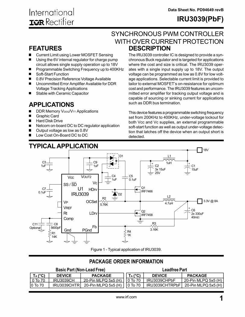
IRU3039(PbF)
1www.irf.com
DESCRIPTIONThe IRU3039 controller IC is designed to provide a syn-chronous Buck regulator and is targeted for applicationswhere the cost and size is critical. The IRU3039 oper-ates with a single input supply up to 18V. The outputvoltage can be programmed as low as 0.8V for low volt-age applications. Selectable current limit is provided totailor to external MOSFET’s on-resistance for optimumcost and performance. The IRU3039 features an uncom-mitted error amplifier for tracking output voltage and iscapable of sourcing or sinking current for applicationssuch as DDR bus termination.
This device features a programmable switching frequencyset from 200KHz to 400KHz, under-voltage lockout forboth Vcc and Vc supplies, an external programmablesoft-start function as well as output under-voltage detec-tion that latches off the device when an output short isdetected.
Current Limit using Lower MOSFET SensingUsing the 6V internal regulator for charge pumpcircuit allows single supply operation up to 18VProgrammable Switching Frequency up to 400KHzSoft-Start Function0.8V Precision Reference Voltage AvailableUncommitted Error Amplifier Available for DDRVoltage Tracking ApplicationsStable with Ceramic Capacitor
FEATURES
SYNCHRONOUS PWM CONTROLLERWITH OVER CURRENT PROTECTION
APPLICATIONSDDR Memory VDDQ/VTT ApplicationsGraphic CardHard Disk DriveNetcom on-board DC to DC regulator applicationOutput voltage as low as 0.8VLow Cost On-Board DC to DC
Data Sheet No. PD94649 revB
Figure 1 - Typical application of IRU3039.
TYPICAL APPLICATION
IRU3039U1
VccVc
HDrv
LDrv
FbGnd
Comp
SS / SD
C31uF
C70.1uF
C85600pF
R114K
Q1IRF7466
Q2IRF7458
L2
4.7uH
L1
1uHC23x 15uF25V
C115uF
3.3V @ 8A
C62x 330uF40mΩ
Rt
18V
OCSet
VOUT2 C50.1uF
D1
R2
PGnd
R3
R41K
VREF
VP
3.16K
5.76K
C41uF
C91uF
C11Optional
D2
PACKAGE ORDER INFORMATION
TA (°C) DEVICE PACKAGE 0 To 70 IRU3039CH 20-Pin MLPQ 5x5 (H) 0 To 70 IRU3039CHTR 20-Pin MLPQ 5x5 (H)
Basic Part (Non-Lead Free) Leadfree Part TA (°C) DEVICE PACKAGE 0 To 70 IRU3039CHPbF 20-Pin MLPQ 5x5 (H) 0 To 70 IRU3039CHTRPbF 20-Pin MLPQ 5x5 (H)
2
IRU3039(PbF)
www.irf.com
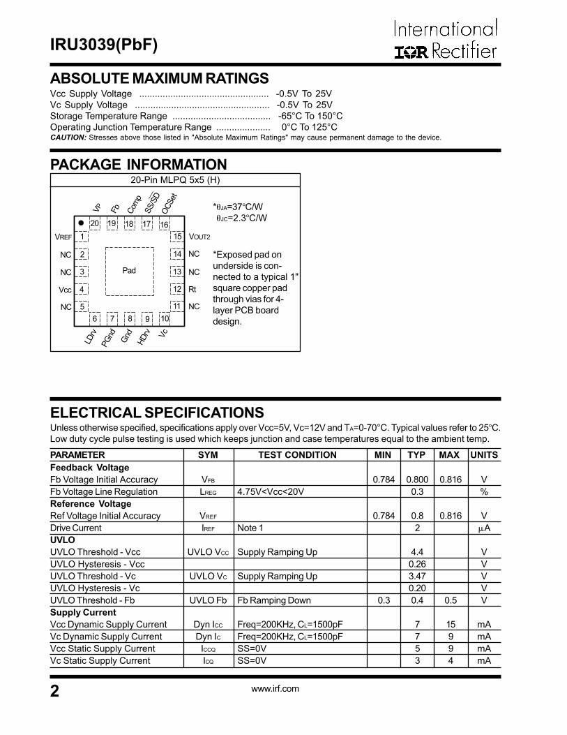
ABSOLUTE MAXIMUM RATINGSVcc Supply Voltage .................................................. -0.5V To 25VVc Supply Voltage .................................................... -0.5V To 25VStorage Temperature Range ...................................... -65°C To 150°COperating Junction Temperature Range ..................... 0°C To 125°CCAUTION: Stresses above those listed in "Absolute Maximum Ratings" may cause permanent damage to the device.
PARAMETER SYM TEST CONDITION MIN TYP MAX UNITSFeedback VoltageFb Voltage Initial AccuracyFb Voltage Line RegulationReference VoltageRef Voltage Initial AccuracyDrive CurrentUVLOUVLO Threshold - VccUVLO Hysteresis - VccUVLO Threshold - VcUVLO Hysteresis - VcUVLO Threshold - FbSupply CurrentVcc Dynamic Supply CurrentVc Dynamic Supply CurrentVcc Static Supply CurrentVc Static Supply Current
4.75V<Vcc<20V
Note 1
Supply Ramping Up
Supply Ramping Up
Fb Ramping Down
Freq=200KHz, CL=1500pFFreq=200KHz, CL=1500pFSS=0VSS=0V
0.784
0.784
0.3
0.8000.3
0.82
4.40.263.470.200.4
7753
0.816
0.816
0.5
15994
V%
VµA
VVVVV
mAmAmAmA
*θJA=37 C/W θJC=2.3 C/W
VFB
LREG
VREF
IREF
UVLO VCC
UVLO VC
UVLO Fb
Dyn ICC
Dyn IC
ICCQ
ICQ
ELECTRICAL SPECIFICATIONSUnless otherwise specified, specifications apply over Vcc=5V, Vc=12V and TA=0-70°C. Typical values refer to 25 C.Low duty cycle pulse testing is used which keeps junction and case temperatures equal to the ambient temp.
PACKAGE INFORMATION 20-Pin MLPQ 5x5 (H)
*Exposed pad onunderside is con-nected to a typical 1"square copper padthrough vias for 4-layer PCB boarddesign.10
VOUT2
NC
NC
Rt
NC
LDrv
PGnd Gnd
HDrv Vc
VREF
NC
NC
Vcc
NC
VP Fb Comp
SS/S
DOC
Set
1
2
3
4
56 7 8 9
11
12
13
14
151617181920
Pad

IRU3039(PbF)
3www.irf.com
PARAMETER SYM TEST CONDITION MIN TYP MAX UNITSError AmpFb Voltage Input Bias CurrentFb Voltage Input Bias CurrentTransconductanceVP Voltage RangeSoft-Start SectionCharge CurrentOscillator SectionFrequencyRamp AmplitudeOutput DriversLo Drive Rise TimeHi Drive Rise TimeLo Drive Fall TimeHi Drive Fall TimeDead Band TimeMax Duty CycleMin Duty CycleInternal RegulatorOutput VoltageDrive CurrentCurrent LimitOC Threshold Set CurrentOC Comp Off-Set Voltage
SS=3VSS=0V
Note 1
SS=0VRt=OpenRt=GndNote 1
CLOAD=1500pF, VCC=12VCLOAD=1500pF, VCC=12VCLOAD=1500pFCLOAD=1500pFHDrv going Hi or LowFb=0.6V, Freq=200KHzFb=1.0V
Vcc=12V
-130
0.8
14
5.740
21-2
+0.0855700
222004001.25
4040404010088
665
281.5
µAµA
µmhoV
µAKHz
VPP
nsnsnsnsns%%
VmA
µAmV
+170
1.5
35
100100100100
0
6.3
355
IFB1
IFB2
VP
SS IBFreq
VRAMP
Tr(LO)
Tr(HI)
Tf(LO)
Tf(HI)
TDB
DMAX
DMIN
VOUT2
IOUT2
IOCSET
VOC(OFFSET)
Note 1: Guaranteed by design but not tested for production.
Reference Voltage. This pin can source current about 2µA.This pin provides biasing for the internal blocks of the IC as well as power for the low sideFET driver. A minimum of 1µF, high frequency capacitor must be connected from this pinto ground to provide peak drive current capability.Output driver for the synchronous power MOSFET.This pin serves as the separate ground for MOSFET's driver and should be connected tosystem's ground plane.This pin serves as analog ground for internal reference and control circuitry. A high fre-quency capacitor must be connected from Vcc pin to this pin for noise free operation.Output driver for the high side power MOSFET. This pin should not go negative (belowground), this may cause problem for the gate drive circuit. It can happen when the inductorcurrent goes negative (Source/Sink), soft-start at no load and for the fast load transientfrom full load to no load. To prevent negative voltage at gate drive, a low forward voltagedrop diode might be connected between this pin and ground.This pin is connected to a voltage that must be at least 4V higher than the bus voltage ofthe switcher (assuming 5V threshold MOSFET) and powers the high side output driver. Aminimum of 1µF, high frequency capacitor must be connected from this pin to ground toprovide peak drive current capability.The switching frequency can be Programmed between 200KHz and 400KHz by connect-ing a resistor between Rt and Gnd. By floating the pin, the switching frequency will be200KHz and by grounding the pin, the switching frequency will be 400KHz.
PIN# PIN SYMBOL PIN DESCRIPTION14
67
8
9
10
12
VREF
Vcc
LDrvPGnd
Gnd
HDrv
Vc
Rt
PIN DESCRIPTIONS

4
IRU3039(PbF)
www.irf.com
Figure 2 - Simplified block diagram of the IRU3039.
BLOCK DIAGRAM
PIN DESCRIPTIONS
Output of internal regulator. The output is protected for short circuit. A high frequencycapacitor is recommended to be connected from this pin to ground.This pin is connected to the Drain of the lower MOSFET via an external resister and itprovides the positive sensing for the internal current sensing circuitry. The external resis-tor programs the current limit threshold depending on the RDS(ON) of the power MOSFET.An external capacitor can be placed in parallel with the programming resistor to providehigh frequency noise filtering.This pin provides soft-start for the switching regulator. An internal current source chargesan external capacitor that is connected from this pin to ground which ramps up the outputof the switching regulator, preventing it from overshooting as well as limiting the inputcurrent. The converter can be shutdown by pulling this pin down below 0.4V.Compensation pin of the error amplifier. An external resistor and capacitor network istypically connected from this pin to ground to provide loop compensation.This pin is connected directly to the output of the switching regulator via resistor divider toprovide feedback to the Error amplifier.Non-inverting input of error amplifier.No connection.
PIN# PIN SYMBOL PIN DESCRIPTION15
16
17
18
19
202,3,5,11,13,14
VOUT2
OCSet
SS / SD
Comp
Fb
VP
NC
22uA
64uA Max
POR
Oscillator
Error Amp
Ct
Error Comp
Reset Dom
POR
0.4VFbLo Comp
Vc
HDrv
Vcc
LDrv
PGnd
Vcc
4V
Vc
3.5V
0.2V
0.2V
BiasGenerator
3V
1.25V
POR
SS / SD
Fb
Comp
25K
25K
3V
R
S
Q
Rt
Gnd
Rt17
19
18
12
10
9
6
7
8OC CompOCSet
3V
28uA
Regulator6V VOUT2
16
15
VREF 1.25V1
VP 20
Enbl
4
0.8V

IRU3039(PbF)
5www.irf.com
THEORY OF OPERATIONIntroductionThe IRU3039 is a fixed frequency, voltage mode syn-chronous controller and consists of a precision refer-ence voltage, an uncommitted error amplifier, an internaloscillator, a PWM comparator, an internal regulator, acomparator for current limit, gate drivers, soft-start andshutdown circuits (see Block Diagram).
The output voltage of the synchronous converter is setand controlled by the output of the error amplifier; this isthe amplified error signal from the sensed output voltageand the voltage on non-inverting input of error amplifier(VP).This voltage is compared to a fixed frequency linearsawtooth ramp and generates fixed frequency pulses ofvariable duty-cycle, which drives the two N-channel ex-ternal MOSFETs.
The timing of the IC is provided through an internal oscil-lator circuit which uses on-chip capacitor. The oscilla-tion frequency is programmable between 200KHz to400KHz by using an external resistor. Figure 14 showsswitching frequency vs. external resistor (Rt).
Soft-StartThe IRU3039 has a programmable soft-start to controlthe output voltage rise and limit the current surge at thestart-up. To ensure correct start-up, the soft-start se-quence initiates when the Vc and Vcc rise above theirthreshold (3.4V and 4.4V respectively) and generatesthe Power On Reset (POR) signal. Soft-start functionoperates by sourcing an internal current to charge anexternal capacitor to about 3V. Initially, the soft-start func-tion clamps the E/A’s output of the PWM converter anddisables the short circuit protection. During the powerup, the output starts at zero and voltage at Fb is below0.4V. The feedback UVLO is disabled during this timeby injecting a current (64µA) into the Fb. This generatesa voltage about 1.6V (64µA×25K) across the negativeinput of E/A and positive input of the feedback UVLOcomparator (see Figure 3).
Figure 3 - Soft-start circuit for IRU3039.
The magnitude of this current is inversely proportional tothe voltage at soft-start pin.
The 20µA current source starts to charge up the exter-nal capacitor. In the mean time, the soft-start voltageramps up, the current flowing into Fb pin starts to de-crease linearly and so does the voltage at the positivepin of feedback UVLO comparator and the voltage nega-tive input of E/A.
When the soft-start capacitor is around 1V, the currentflowing into the Fb pin is approximately 32µA. The volt-age at the positive input of the E/A is approximately:
The E/A will start to operate and the output voltage startsto increase. As the soft-start capacitor voltage contin-ues to go up, the current flowing into the Fb pin will keepdecreasing. Because the voltage at pin of E/A is regu-lated to reference voltage 0.8V, the voltage at the Fb is:
32µA×25K = 0.8V
VFB = 0.8-25K×(Injected Current)
20uA
64uAMax
POR
Error Amp
64uA×25K=1.6VWhen SS=0
POR
0.4V
Feeback UVLO Comp
SS/SD
Fb
Comp25K
0.8V
25K
HDrv
LDrv
3V

6
IRU3039(PbF)
www.irf.com
Soft-Start Voltage
Voltage at negative inputof Error Amp and Feedback
UVLO comparator
Voltage at Fb pin
Current flowinginto Fb pin
64uA
0uA
0V
0.8V
≅ 1.6V0.8V
0V
3V
≅ 2V
≅ 1V
Output of UVLOPOR
CSS ≅ 20µA×TSTART/1V
20µA×TSTART/CSS = 2V-1V
The feedback voltage increases linearly as the injectingcurrent goes down. The injecting current drops to zerowhen soft-start voltage is around 2V and the output volt-age goes into steady state.
As shown in Figure 4, the positive pin of feedback UVLOcomparator is always higher than 0.4V, therefore, feed-back UVLO is not functional during soft-start.
Figure 4 - Theoretical operational waveformsduring soft-start.
the output start-up time is the time period when soft-start capacitor voltage increases from 1V to 2V. The start-up time will be dependent on the size of the externalsoft-start capacitor. The start-up time can be estimatedby:
For a given start up time, the soft-start capacitor can beestimated as:
Internal RegulatorThe regulator powers directly from Vcc and generates aregulated voltage (6V @ 40mA). The output is protectedfor short circuit. This voltage can be used for chargepump circuitry as shown in Figure 1.
Supply Voltage Under-Voltage LockoutThe under-voltage lockout circuit assures that theMOSFET driver outputs remain in the off state wheneverthe supply voltage drops below set parameters. Lockoutoccurs if Vc or Vcc fall below 3.4V and 4.4V respec-tively. Normal operation resumes once Vc and Vcc riseabove the set values.
VOCSET = IOCSET×RSET-RDS(ON)×iL ---(1)
ShutdownThe converter can be shutdown by pulling the soft-startpin below 0.4V. The control MOSFET turns off and thesynchronous MOSFET turns on during shutdown.
Over-Current ProtectionOver-current protection is achieved with a cycle by cyclescheme and it is performed by sensing current throughthe RDS(ON) of low side MOSFET. As shown in Figure 5,an external resistor (RSET) is connected between OCSetpin and the drain of low side MOSFET (Q2) and sets thecurrent limit set point. The internal current source devel-ops a voltage across RSET. When the low side switch isturned on, the inductor current flows through the Q2 andresults a voltage which is given by:
Figure 5 - Diagram of the over current sensing.
When voltage VOCSET is below zero, the current sensingcomparator flips and disables the oscillator. The highside MOSFET is turned off and the low side MOSFET isturned on until the inductor current reduces to belowcurrent set value. The critical inductor current can becalculated by setting:
If the over-current condition is temporary and goes awayquickly, the IRU3039 will resume its normal operation.
If output is shorted or over-current condition persists,the output voltage will keep going down until it is below0.4V. Then the output under-voltage lock out comparatorgoes high and turns off both MOSFETs. The operationwaveforms are shown in Figure 6.
L1RSET
IRU3039OCSet
IOCSET
VOUT
Osc
Q1
Q2
ISET = IL(CRITICAL) = ---(2)RSET×IOCSET
RDS(ON)
VOCSET = IOCSET×RSET - RDS(ON)×IL = 0

IRU3039(PbF)
7www.irf.com
Figure 6 - Diagram of over-current operation.
Operation in current limit is shown in Figure 7, the highside MOSFET is turned off and inductor current starts todecrease. Because the output inductor current is higherthan the current limit setpoint (ISET), the over-current com-parator keeps high until the inductor current decreasesto be below ISET. Then another cycle starts.
During over-current mode, the valley inductor current is:
The peak inductor current is given as:
To avoid undesirable trigger of over-current protection,this relationship must be satisfied:
Figure 7 - Operation waveforms during current limit.
iL(VALLEY) = ISET
From Figure 7, the average inductor current during thecurrent limit mode is:
The inductor's ripple current can be expressed as:
Combination of above equation and (4) results in:
Combination of equations (5) and (2) results in the rela-tionship between RSET and output current limit.
From the above analysis, the current limit is not onlydependent on the current setting resistor RSET and RDS(ON)
of low side MOSFET but it is also dependent on theinput voltage, output voltage, inductance and switchingfrequency as well.
The cycle-by-cycle over-current limit will hold for a cer-tain amount of time, until the output voltage drops below0.4V, the under-voltage lock out activates and latchesoff the output driver. The operation waveform is shown inFigure 7. Normal operation will resume after IRU3039 ispowered up again.
IL(PEAK) = ISET+(VIN-VOUT)×tON/L ---(3)
ISET=iL(VALLEY)
iL(PEAK)
tON tOFF
iL(AVG)
Current Limit Comparator Output
Inductor Current
HDrv
Feedbackvoltage
Switching frequency
High Side MOSFET turn on time (tON)
Average Inductor Current
IOUT
IOUT
IOUT
IOUT
DMAX/FS(NOM)
FS(NOM)
0.4V
VREF
<IL>=IOUT
Normal operation
Over Current Limit Mode
Shutdown by UVLO
IO(LIM) IO(MAX)
VOUTFS(NOM)×VIN
ISET IO(NOM) - ∆IPK-PK(NOM)
2
ISET = IO(LIM) - ---(5)(VIN-VOUT)×VOUT
2×fS×L×VIN( )
RSET = × IO(LIM) - ---(6)RDS(ON)
IOCSET [ ( )](VIN-VOUT)×VOUT
2×fS×L×VIN
Where:IO(LIM) = The Output Current Limit. Typical is 50%higher than nominal output currentVIN = Maximum Input VoltageVOUT = Output VoltagefS = Switching FrequencyL = Output InductorRDS(ON) = RDS(ON) of Low Side MOSFETIOCSET = OC Threshold Set Current
(VIN - VOUT)×VOUT
VIN×L×fS∆IPK-PK(LIM) =
IO(LIM) = ISET + ---(4)∆IPK-PK(LIM)
2

8
IRU3039(PbF)
www.irf.com
APPLICATION INFORMATIONDesign Example:The following example is a typical application for IRU3039,the schematic is Figure 17 on page 16.
Output Voltage ProgrammingOutput voltage is programmed by reference voltage andexternal voltage divider. The Fb pin is the inverting inputof the error amplifier, which is referenced to the voltageon non-inverting pin of error amplifier. For this applica-tion, this pin (VP) is connected to reference voltage (VREF).The output voltage is defined by using the following equa-tion:
When an external resistor divider is connected to theoutput as shown in Figure 8.
Figure 8 - Typical application of the IRU3039 forprogramming the output voltage.
Equation (7) can be rewritten as:
Choose R5 = 1KThis will result to R6 = 3.16K
If the high value feedback resistors are used, the inputbias current of the Fb pin could cause a slight increasein output voltage. The output voltage set point can bemore accurate by using precision resistor.
Soft-Start ProgrammingThe soft-start timing can be programmed by selectingthe soft-start capacitance value. The start-up time of theconverter can be calculated by using:
For a start-up time of 5ms, the soft-start capacitor willbe 0.1µF. Choose a ceramic capacitor at 0.1µF.
Boost Supply VcTo drive the high side switch, it is necessary to supply agate voltage at least 4V grater than the bus voltage. Thisis achieved by using a charge pump configuration asshown in Figure 9. This method is simple and inexpen-sive. The operation of the circuit is as follows: when thelower MOSFET is turned on, the capacitor (C1) is pulleddown to ground and charges, up to VOUT2 value, throughthe diode (D1). The bus voltage will be added to thisvoltage when upper MOSFET turns on in next cycle,and providing supply voltage (Vc) through diode (D2). Vcis approximately:
Capacitors in the range of 0.1µF and 1µF are generallyadequate for most applications. The diode must be afast recovery device to minimize the amount of chargefed back from the charge pump capacitor into VOUT2. Thediodes need to be able to block the full power rail volt-age, which is seen when the high side MOSFET isswitched on. For low voltage application, schottky di-odes can be used to minimize forward drop across thediodes at start up.
Figure 9 - Charge pump circuit.
Input Capacitor SelectionThe input filter capacitor should be based on how muchripple the supply can tolerate on the DC input line. Theripple current generated during the on time of upperMOSFET should be provided by input capacitor. The RMSvalue of this ripple is expressed by:
VOUT = VP × 1 + ---(7)R6
R5
VP = VREF = 0.8V
( )
R6 = R5 × - 1VOUT
VP( )
Fb
IRU3039VOUT
R5
R6
VREF
VP
Vc ≅ VOUT2 + VBUS - (VD1 + VD2)
VIN = 18VVOUT = 3.3VIOUT = 8A∆VOUT = 100mV (output voltage ripple ≅ 3% of VOUT)fS = 200KHz
L2
IRU3039
D1
C1Vc
HDrv
RegulatorQ1
Q2
VOUT2
C2VBUS
D2C3
Css ≅ 20×tSTART (µF) ---(8)
Where tSTART is the desired start-up time (ms)

IRU3039(PbF)
9www.irf.com
For higher efficiency, a low ESR capacitor is recom-mended. Choose three Poscap from Sanyo 25TQC15M(25V, 15µF, 90mΩ) with a maximum allowable ripplecurrent of 3A.
Inductor SelectionThe inductor is selected based on operating frequency,transient performance and allowable output voltage ripple.
Low inductor value results to faster response to stepload (high ∆i/∆t) and smaller size but will cause largeroutput ripple due to increase of inductor ripple current.As a rule of thumb, select an inductor that produces aripple current of 10-40% of full load DC.
For the buck converter, the inductor value for desiredoperating ripple current can be determined using the fol-lowing relation:
If ∆i = 37%(IO), then the output inductor will be:
The Coilcraft DO5022HC series provides a range of in-ductors in different values, low profile suitable for largecurrents, 4.7µH, 13A is a good choice for this applica-tion. This will result to a ripple approximately 37% ofoutput current.
Output Capacitor SelectionThe criteria to select the output capacitor is normallybased on the value of the Effective Series Resistance(ESR). In general, the output capacitor must have lowenough ESR to meet output ripple and load transient
L = 4.65µH2
2
PCOND(Upper Switch) = ILOAD×RDS(ON)×D×ϑ
PCOND(Lower Switch) = ILOAD×RDS(ON)×(1 - D)×ϑ
ϑ = RDS(ON) Temperature Dependency
For VIN=20V, IOUT=8A and D=0.165, the IRMS=3A
IRMS = IOUT D×(1-D) ---(9)
Where:D is the Duty Cycle, D=VOUT/VIN.
IRMS is the RMS value of the input capacitor current.IOUT is the output current for each channel.
VIN - VOUT = L× ; ∆t = D× ; D =1fS
VOUT
VIN
∆i∆t
L = (VIN - VOUT)× ---(11)VOUT
VIN×∆i×fSWhere:VIN = Maximum Input VoltageVOUT = Output Voltage∆i = Inductor Ripple CurrentfS = Switching Frequency∆t = Turn On TimeD = Duty Cycle
Where:∆VO = Output Voltage Ripple∆i = Inductor Ripple Current∆VO = 100mV and ∆I ≅ 40% of 8A = 3.2AThis results to: ESR=31mΩ
ESR ≤ ---(10)∆VO
∆IO
requirements, yet have high enough ESR to satisfy sta-bility requirements. The ESR of the output capacitor iscalculated by the following relationship:
The Sanyo TPC series, Poscap capacitor is a good choice.The 6TPC330M, 330µF, 6.3V has an ESR 40mΩ. Se-lecting two of these capacitors in parallel, results to anESR of ≅ 20mΩ which achieves our low ESR goal.
The capacitor value must be high enough to absorb theinductor's ripple current. The larger the value of capaci-tor, the lower will be the output ripple voltage.
Power MOSFET SelectionThe IRU3039 uses two N-Channel MOSFETs. The se-lections criteria to meet power transfer requirements isbased on maximum drain-source voltage (VDSS), gate-source drive voltage (VGS), maximum output current, On-resistance RDS(ON) and thermal management.
The MOSFET must have a maximum operating voltage(VDSS) exceeding the maximum input voltage (VIN).
The gate drive requirement is almost the same for bothMOSFETs. Logic-level transistor can be used and cau-tion should be taken with devices at very low VGS to pre-vent undesired turn-on of the complementary MOSFET,which results a shoot-through current.
The total power dissipation for MOSFETs includes con-duction and switching losses. For the Buck converter,the average inductor current is equal to the DC load cur-rent. The conduction loss is defined as:
The RDS(ON) temperature dependency should be consid-ered for the worst case operation. This is typically givenin the MOSFET data sheet. Ensure that the conductionlosses and switching losses do not exceed the packageratings or violate the overall thermal budget.

10
IRU3039(PbF)
www.irf.com
Choose IRF7466 for control MOSFET and IRF7458 forsynchronous MOSFET. These devices provide low on-resistance in a compact SOIC 8-Pin package.
The MOSFETs have the following data:
The total conduction losses will be:
The switching loss is more difficult to calculate, eventhough the switching transition is well understood. Thereason is the effect of the parasitic components andswitching times during the switching procedures suchas turn-on / turnoff delays and rise and fall times. Thecontrol MOSFET contributes to the majority of the switch-ing losses in synchronous Buck converter. The synchro-nous MOSFET turns on under zero voltage conditions,therefore, the turn on losses for synchronous MOSFETcan be neglected. With a linear approximation, the totalswitching loss can be expressed as:
The switching time waveform is shown in Figure 10.
Figure 10 - Switching time waveforms.
From IRF7466 data sheet we obtain:
These values are taken under a certain condition test.For more details please refer to the IRF7466 and IRF7458data sheets.
By using equation (12), we can calculate the total switch-ing losses.
Programming the Over-Current LimitThe over-current threshold can be set by connecting aresistor (RSET) from drain of low side MOSFET to theOCSet pin. The resistor can be calculated by using equa-tion (2).
The RDS(ON) has a positive temperature coefficient and itshould be considered for the worse case operation.
Feedback CompensationThe IRU3039 is a voltage mode controller; the controlloop is a single voltage feedback path including erroramplifier and error comparator. To achieve fast transientresponse and accurate output regulation, a compensa-tion circuit is necessary. The goal of the compensationnetwork is to provide a closed loop transfer function withthe highest 0dB crossing frequency and adequate phasemargin (greater than 45 ).
The output LC filter introduces a double pole, –40dB/decade gain slope above its corner resonant frequency,and a total phase lag of 180 (see Figure 11). The Reso-nant frequency of the LC filter is expressed as follows:
Figure 11 shows gain and phase of the LC filter. Sincewe already have 180 phase shift just from the outputfilter, the system risks being unstable.
Figure 11 - Gain and phase of LC filter.
PCON(TOTAL) = PCON(UPPER) + PCON(LOWER)
PCON(TOTAL) = 0.85W
PSW(TOTAL) = 92mWIRF7466VDSS = 30VID = 11ARDS(ON) = 12.5mΩ
IRF7458VDSS = 30VID = 14ARDS(ON) = 8mΩ
Where:VDS(OFF) = Drain to Source Voltage at off timetr = Rise Timetf = Fall TimeT = Switching PeriodILOAD = Load Current
PSW = ILOAD ---(12)×VDS(OFF)
2tr + tf
T×
IRF7466tr = 2.8nstf = 3.6ns
FLC = ---(13)1
2π× LO×CO
RDS(ON) = 8mΩ×1.5 = 12mΩISET ≅ IO(LIM) = 8A×1.5 = 12A(50% over nominal output current)This results to:RSET = 5.76KΩ
VDS
VGS
10%
90%
td(ON) td(OFF)tr tf
Gain
FLC
0dB
Phase
0
FLC-180
Frequency Frequency
-40dB/decade

IRU3039(PbF)
11www.irf.com
The IRU3039’s error amplifier is a differential-inputtransconductance amplifier. The output is available forDC gain control or AC phase compensation.
The E/A can be compensated with or without the use oflocal feedback. When operated without local feedback,the transconductance properties of the E/A become evi-dent and can be used to cancel one of the output filterpoles. This will be accomplished with a series RC circuitfrom Comp pin to ground as shown in Figure 12.
Note that this method requires that the output capacitorshould have enough ESR to satisfy stability requirements.In general, the output capacitor’s ESR generates a zerotypically at 5KHz to 50KHz which is essential for anacceptable phase margin.
The ESR zero of the output capacitor expressed as fol-lows:
Figure 12 - Compensation network without localfeedback and its asymptotic gain plot.
The transfer function (Ve / VOUT) is given by:
The (s) indicates that the transfer function varies as afunction of frequency. This configuration introduces a gainand zero, expressed by:
|H(s)| is the gain at zero cross frequency.
First select the desired zero-crossover frequency (Fo):
Use the following equation to calculate R4:
Where:VIN = Maximum Input VoltageVOSC = Oscillator Ramp VoltageFo = Crossover FrequencyFESR = Zero Frequency of the Output CapacitorFLC = Resonant Frequency of the Output FilterR5 and R6 = Resistor Dividers for Output Voltage Programminggm = Error Amplifier Transconductance
This results to R4=12.08KChoose R4=14K
To cancel one of the LC filter poles, place the zero be-fore the LC filter resonant frequency pole:
Using equations (17) and (19) to calculate C9, we get:
One more capacitor is sometimes added in parallel withC9 and R4. This introduces one more pole which is mainlyused to suppress the switching noise. The additionalpole is given by:
The pole sets to one half of switching frequency whichresults in the capacitor CPOLE:
C9 ≅ 5300pF; Choose C9 =5600pF
VOUT
Vp=VREF
R5
R6
R4
C9
VeE/A
FZ
H(s) dB
Frequency
Gain(dB)
FbComp
FESR = ---(14)12π×ESR×Co
H(s) = gm× × ---(15)( )R5
R6 + R5
1 + sR4C9
sC9
FLC = 2.8KHzR5 = 1KR6 = 3.16Kgm = 700µmho
For:VIN = 18VVOSC = 3.3VFo = 20KHzFESR = 12KHz
R4 = × × × ---(18)Fo×FESR
FLC2VOSC
VIN
R5 + R6
R5
1gm
Fo > FESR and FO ≤ (1/5 ~ 1/10)×fS
For:Lo = 4.7µHCo = 660µF
FZ ≅ 75%FLC
FZ ≅ 0.75×1
2π LO × CO---(19)
FZ = 2.1KHzR4 = 14K
FP =2π×R4×
1C9×CPOLE
C9 + CPOLE
CPOLE = ≅
for FP << fS2
1π×R4×fS
π×R4×fS -
11C9
FZ = ---(17)12π×R4×C9
|H(s=j×2π×FO)| = gm× ×R4 ---(16)R5
R6×R5

12
IRU3039(PbF)
www.irf.com
For a general solution for unconditionally stability forceramic capacitor with very low ESR and any type ofoutput capacitors, in a wide range of ESR values weshould implement local feedback with a compensationnetwork. The typically used compensation network forvoltage-mode controller is shown in Figure 13.
Figure 13 - Compensation network with localfeedback and its asymptotic gain plot.
In such configuration, the transfer function is given by:
The error amplifier gain is independent of the transcon-ductance under the following condition:
By replacing ZIN and Zf according to Figure 9, the trans-former function can be expressed as:
As known, transconductance amplifier has high imped-ance (current source) output, therefore, consider shouldbe taken when loading the E/A output. It may exceed itssource/sink output current capability, so that the ampli-fier will not be able to swing its output voltage over thenecessary range.
The compensation network has three poles and two ze-ros and they are expressed as follows:
Cross Over Frequency:
The stability requirement will be satisfied by placing thepoles and zeros of the compensation network accordingto following design rules. The consideration has beentaken to satisfy condition (20) regarding transconduc-tance error amplifier.
These design rules will give a crossover frequency ap-proximately one-tenth of the switching frequency. Thehigher the band width, the potentially faster the load tran-sient speed. The gain margin will be large enough toprovide high DC-regulation accuracy (typically -5dB to -12dB). The phase margin should be greater than 45 foroverall stability.
Based on the frequency of the zero generated by ESRversus crossover frequency, the compensation type canbe different. The table below shows the compensationtype and location of crossover frequency.
VOUT
Vp=VREF
R5
R6R8
C10
C12
C11R7
Ve
FZ1 FZ2 FP2 FP3
E/A
Zf
ZIN
Frequency
Gain(dB)
H(s) dB
FbComp
H(s) =1+sR7 ×(1+sR8C10)
(1+sR7C11)×[1+sC10(R6+R8)]×
[ ( )]1
sR6(C12+C11) C12C11
C12+C11
gmZf >> 1 and gmZIN >>1 ---(20)
1 - gmZf
1 + gmZIN
VeVOUT
=
Where:VIN = Maximum Input VoltageVOSC = Oscillator Ramp VoltageLo = Output InductorCo = Total Output Capacitors
FO = R7×C10× ×VIN
VOSC
12π×Lo×Co ---(21)
FP1 = 0
12π×C10×(R6 + R8)FZ2 = ≅ 1
2π×C10×R6
FZ1 = 12π×R7×C11
FP3 = ≅1
2π×R7×
12π×R7×C12
FP2 = 12π×R8×C10
( )C12×C11
C12+C11
Detail information is dicussed in application Note AN-1043 which can be downloaded from the IR Web-Site.
CompensatorType
Type II (PI)
Type III (PID)Method AType III (PID)Method B
Location of ZeroCrossover Frequency
(FO)FPO < FZO < FO < fS/2
FPO < FO < FZO < fS/2
FPO < FO < fS/2 < FZO
TypicalOutput
CapacitorElectrolytic,
TantalumTantalum,CeramicCeramic
Table - The compensation type and location of zerocrossover frequency.

IRU3039(PbF)
13www.irf.com
Layout ConsiderationThe layout is very important when designing high fre-quency switching converters. Layout will affect noisepickup and can cause a good design to perform withless than expected results.
Start to place the power components. Make all the con-nections in the top layer with wide, copper filled areas.The inductor, output capacitor and the MOSFET shouldbe close to each other as possible. This helps to reducethe EMI radiated by the power traces due to the highswitching currents through them. Place input capacitordirectly to the drain of the high-side MOSFET. To reduce
Figure 14 - Switching Frequency versus Resistor.
the ESR, replace the single input capacitor with two par-allel units. The feedback part of the system should bekept away from the inductor and other noise sourcesand be placed close to the IC. In multilayer PCB, useone layer as power ground plane and have a separatecontrol circuit ground (analog ground), to which all sig-nals are referenced. The goal is to localize the high cur-rent path to a separate loop that does not interfere withthe more sensitive analog control function. These twogrounds must be connected together on the PC boardlayout at a single point.
200
250
300
350
400
450
0 50 100 150 200 250 300 350 400 450Rt (KΩ)
Freq
uenc
y (K
Hz)

14
IRU3039(PbF)
www.irf.com
TYPICAL APPLICATION
Figure 15 - Typical application of the IRU3039 with two input supplies.
IRU3039U1
Vcc VcHDrv
LDrv
FbGnd
Comp
SS / SD
C31uF
C70.1uF
C82200pF
R128K
Q1IRF7457
Q2IRF7457
L2
3.3uH
L1
1uHC2 2x 150uF
C147uF
VOUT2.5V @ 10A
C62x 330uF, 40mΩRt
5V
OCSet
VOUT2
C41uF
R2
PGnd
R3
R41K
VREF
VP
+12V
7.12K
2.15K
D1

IRU3039(PbF)
15www.irf.com
TYPICAL APPLICATION
Figure 16 - Typical application of IRU3039 for DDR memory when IRU3039generates VCORE and IRU3038 generates the termination voltage.
IRU3039U1
C11uF
C21uF
C60.1uF
C84.7nF
R227K
Q11/2 of IRF7313
Q11/2 of IRF7313
L2
L1
1uHC32x 100uF, 55mΩ10TPB100M
C447uF
VDDQ1.8V @ 5AC7
2x 330uF, 40mΩ 6TPC330M
12V5V
IRU3038U2
Vcc Vc
HDrv
LDrv
FbComp
SS / SD
C91uF
C101uF
C120.15uF
C145.6nF
R613K
Q21/2 of IRF7313
Q21/2 of IRF7313
L3
4.7uH VTT (0.9V @ 3A)C132x 330uF, 40mΩ6TPC330M
12V
PGndRt
VP
VREF
5V
5V
R1
1.25KR31K
R41K
R51K
4.7uH
C11100uF, 55mΩ10TPB100M
VOUT2
D2
D1
Gnd
CompRt
SS / SD
VP
VREFVcc Vc
HDrv
OCSetLDrv
PGnd
Fb
8K
R7
Gnd

16
IRU3039(PbF)
www.irf.com
DEMO-BOARD APPLICATION18V to 3.3V @ 8A
Ref Desig Description Value Qty Part# Manuf Web site (www.)1111111431123111111
Q1Q2U1D1D2L1L2C1,C2A,B,CC5,6,10C7C8C9A,BC3,11,12C13R4R7R8R9R10
MOSFETMOSFETControllerSchottky DiodeSchottky DiodeInductorInductorCap, PoscapCapacitorCapacitorCapacitorCapacitorCapacitorCapacitorResistorResistorResistorResistorResistor
IRF7466IRF7458IRU3039BAT54SBAT54DS1608C-102DO5022P-472HC25TQC15MECJ-2VF1E104ZECU-V1H562KBGECJ-2VC1H471J6TPB-330MECJ-2VF1C105ZECJ-3YB1E105K
IRIRIRIRIRCoilcraftCoilcraftSanyoPanasonicPanasonicPanasonicSanyoPanasonicPanasonic
irf.com
coilcraft.com
sanyo.commaco.panasonic.co.jp
sanyo.commaco.panasonic.co.jp
30V, 12.5mΩ, 11A30V, 8mΩ, 14ASynchronous PWMFast SwitchingFast Switching1µH, 3A4.7µH, 13A15µF, 25V0.1µF, Y5V, 25V5600pF, X7R, 50V470pF, X7R, 50V330uF, 40mΩ1µF, Y5V, 16V1µF, X7R, 25V5.76K14K4.7Ω3.16K1K
Figure 17 - Demo-board application of the IRU3039.
PARTS LIST
IRU3039U1
VccVc
HDrv
LDrv
FbGnd
Comp
SS / SD
C111uF
C60.1uF
C75600pF
R714K
Q1IRF7466
Q2IRF7458
L2
4.7uH
L1
1uHC2A,B,C3x 15uF25V
C115uF
3.3V @ 8A
C9A,B2x 330uF40mΩ
Rt
18V
OCSet
VOUT2 C50.1uF
D1
R4
PGndR9
R101K
VREF
VP
3.16K
5.76K
C131uF
C8470pF
R84.7Ω
D2
C31uF
C121uF
C100.1uF
IRU3039(PbF)
17www.irf.com
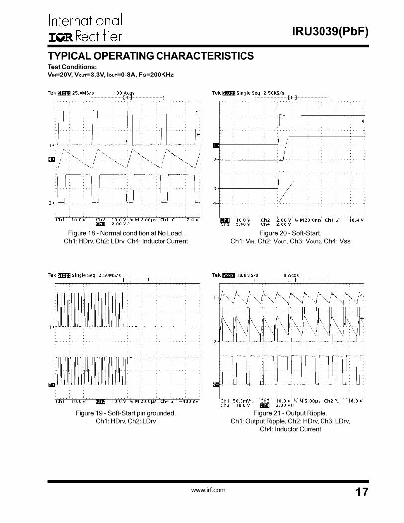
TYPICAL OPERATING CHARACTERISTICSTest Conditions:VIN=20V, VOUT=3.3V, IOUT=0-8A, Fs=200KHz
Figure 19 - Soft-Start pin grounded.Ch1: HDrv, Ch2: LDrv
Figure 21 - Output Ripple.Ch1: Output Ripple, Ch2: HDrv, Ch3: LDrv,
Ch4: Inductor Current
Figure 18 - Normal condition at No Load.Ch1: HDrv, Ch2: LDrv, Ch4: Inductor Current
Figure 20 - Soft-Start.Ch1: VIN, Ch2: VOUT, Ch3: VOUT2, Ch4: Vss

18
IRU3039(PbF)
www.irf.com
TYPICAL OPERATING CHARACTERISTICSTest Conditions:VIN=20V, VOUT=3.3V, IOUT=0-8A, Fs=200KHz
Figure 23 - Load Transient ResponseCh1: VOUT, Ch3: Output Current
0A
8A
Figure 22 - Output shorted at start up.Ch1: VOUT, Ch3: Vss, Ch4: Inductor Current
Figure 24 - Efficiency Measurement.VIN=20V, VOUT=3.3V
7072747678808284868890
0 1 2 3 4 5 6 7 8 9 10 11Output Current (A)
Effic
ienc
y (%
)

IRU3039(PbF)
19www.irf.com
Figure 26 - Frequency vs.TemperatureFS=200KHz
Figure 25 - VREF vs.Temperature Figure 28 - VOUT2 vs.Temperature
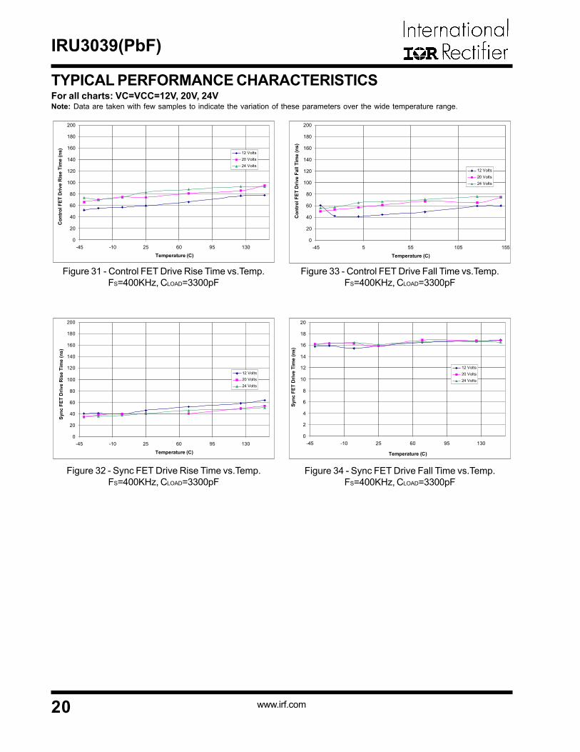
TYPICAL PERFORMANCE CHARACTERISTICSFor all charts: VC=VCC=12V, 20V, 24VNote: Data are taken with few samples to indicate the variation of these parameters over the wide temperature range.
Figure 30 - Deadtime, Sync FET DriveRising Time vs.TemperatureFS=400KHz, CLOAD=3300pF
Figure 29 - Frequency vs.TemperatureFS=400KHz
Figure 27 - Deadtime, Control FET DriveRising Time vs.TemperatureFS=400KHz, CLOAD=3300pF
0.793
0.794
0.795
0.796
0.797
0.798
0.799
0.8
0.801
0.802
-45 -10 25 60 95 130
Temperature (C)
Vref
(V) 12 Volt
20 Volt24 Volt
204
205
206
207
208
209
210
211
212
213
214
215
-45 -10 25 60 95 130
Temperature (C)
Freq
uenc
y (K
Hz)
12 Volt
20 Volt
24 Volt
0
50
100
150
200
-45 -10 25 60 95 130Temperature (C)
Dea
dtim
e, S
witc
h FE
T D
rive
Ris
ing
Tim
e (n
s)
12 Volts20 Volts24 Volts
5.8
5.85
5.9
5.95
6
6.05
6.1
6.15
6.2
-45 -10 25 60 95 130Temperature (C)
Vout
2 (V
)
12 Volt
20 Volt
24 Volt
385
390
395
400
405
410
-45 -10 25 60 95 130
Temperature (C)
Freq
uenc
y (K
Hz) 12 Volt
20 Volt
24 Volt
0
50
100
150
200
-45 -10 25 60 95 130Temperature (C)
Dea
dtim
e, S
ync
FET
Driv
e R
isin
g Ti
me
(ns)
12 Volts
20 Volts24 Volts
20
IRU3039(PbF)
www.irf.com
Figure 31 - Control FET Drive Rise Time vs.Temp.FS=400KHz, CLOAD=3300pF
Figure 33 - Control FET Drive Fall Time vs.Temp.FS=400KHz, CLOAD=3300pF
Figure 34 - Sync FET Drive Fall Time vs.Temp.FS=400KHz, CLOAD=3300pF
Figure 32 - Sync FET Drive Rise Time vs.Temp.FS=400KHz, CLOAD=3300pF
TYPICAL PERFORMANCE CHARACTERISTICSFor all charts: VC=VCC=12V, 20V, 24VNote: Data are taken with few samples to indicate the variation of these parameters over the wide temperature range.
0
20
40
60
80
100
120
140
160
180
200
-45 -10 25 60 95 130Temperature (C)
Con
trol F
ET D
rive
Ris
e Ti
me
(ns) 12 Volts
20 Volts24 Volts
0
20
40
60
80
100
120
140
160
180
200
-45 -10 25 60 95 130
Temperature (C)
Sync
FET
Driv
e R
ise
Tim
e (n
s)
12 Volts20 Volts24 Volts
0
20
40
60
80
100
120
140
160
180
200
-45 5 55 105 155Temperature (C)
Con
trol F
ET D
rive
Fall
Tim
e (n
s)
12 Volts20 Volts24 Volts
0
2
4
6
8
10
12
14
16
18
20
-45 -10 25 60 95 130
Temperature (C)
Sync
FET
Driv
e Ti
me
(ns)
12 Volts20 Volts24 Volts
IRU3039(PbF)
21www.irf.com
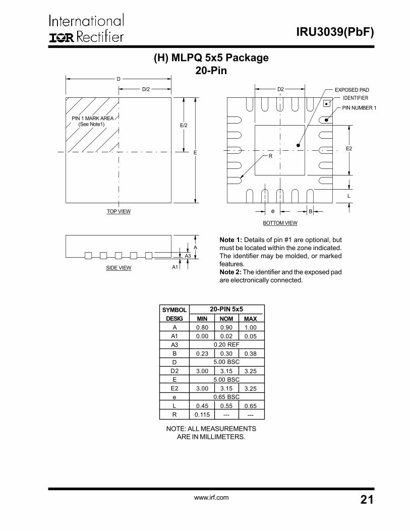
(H) MLPQ 5x5 Package20-Pin
Note 1: Details of pin #1 are optional, butmust be located within the zone indicated.The identifier may be molded, or markedfeatures.Note 2: The identifier and the exposed padare electronically connected.
A3
A1
A
E2E
D/2 D2
e
L
B
EXPOSED PAD
BOTTOM VIEW
TOP VIEW
PIN NUMBER 1
SIDE VIEW
E/2
D
PIN 1 MARK AREA (See Note1)
R
SYMBOLDESIG
AA1A3BD
D2E
E2eLR
MIN0.800.00
0.23
3.00
3.00
0.450.115
NOM0.900.02
0.30
3.15
3.15
0.55---
5.00 BSC
MAX1.000.05
0.38
3.25
3.25
0.65---
5.00 BSC
0.65 BSC
20-PIN 5x5
0.20 REF
NOTE: ALL MEASUREMENTSARE IN MILLIMETERS.
•IDENTIFIER
22
IRU3039(PbF)
www.irf.com
PKGDESIG
H
PACKAGEDESCRIPTION
MLPQ 5x5
PARTSPER TUBE
---
PARTSPER REEL
3000
PACKAGE SHIPMENT METHODPIN
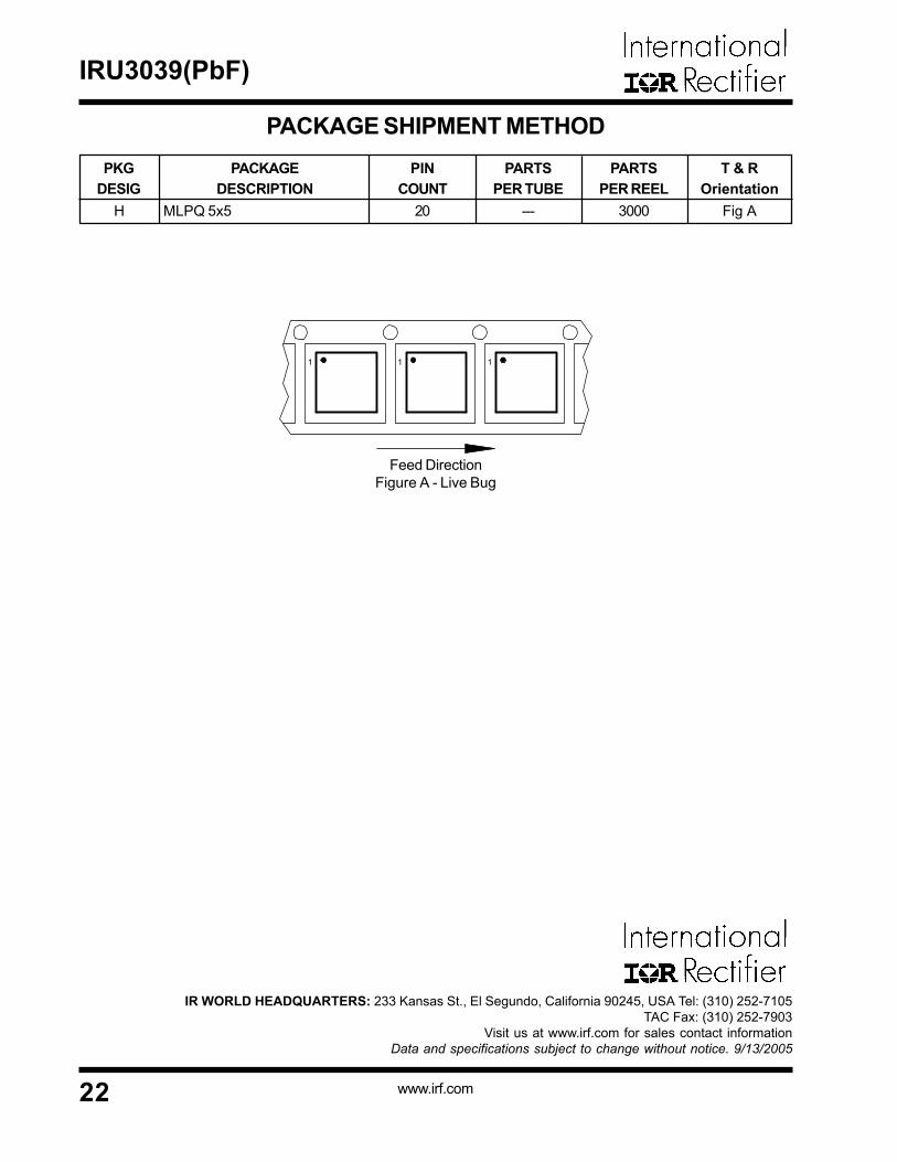
COUNT20
T & ROrientation
Fig A
Feed DirectionFigure A - Live Bug
IR WORLD HEADQUARTERS: 233 Kansas St., El Segundo, California 90245, USA Tel: (310) 252-7105TAC Fax: (310) 252-7903
Visit us at www.irf.com for sales contact informationData and specifications subject to change without notice. 9/13/2005
1 1 1