Embed Size (px)
Citation preview

SLVS367A − MARCH 2001 − REVISED JUNE 2001
1www.ti.com
FEATURES Integrated Drive Regulator (4 V to 14 V)
Adjustable/Adaptive Dead-Time Control
4-A Peak current at VDRV of 14 V
10-V to 15-V Supply Voltage Range
TTL-Compatible Inputs
Internal Schottky Diode Reduces Part Count
Synchronous or Nonsynchronous Operation
Inverting and Noninverting Options
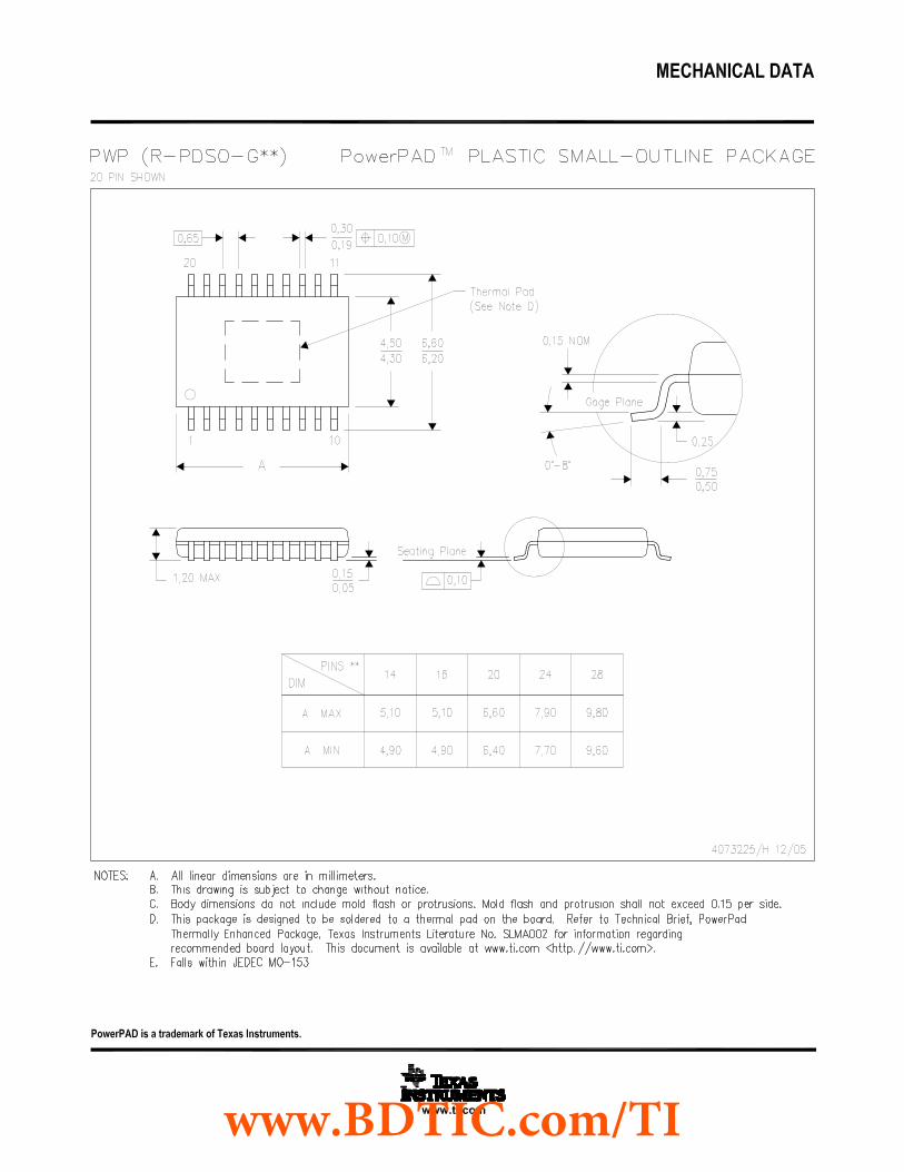
TSSOP PowerPad Package for ExcellentThermal Performance
APPLICATIONS Single or Multiphase Synchronous-Buck
Power Supplies
High-Current DC/DC Power Modules
DESCRIPTION
The TPS2838/39/48/49 devices are MOSFETdrivers designed for high-performancesynchronous power supplies. The drivers cansource and sink up to 4-A peak current at a 14-Vdrive voltage. These are ideal devices to use withpower supply controllers that do not have on-chipdrivers. The low-side driver is capable of drivingloads of 3.3 nF in 10-ns rise/fall times and has40-ns propagation delays at room temperature.
The MOSFET drivers have an integrated 150-mAregulator, so the gate drive voltage can beoptimized for specific MOSFETs. The TPS2848and TPS2849 have a fixed 8-V drive regulator,while the TPS2838/39 allow the drive regulator tobe adjusted from 4 V to 14 V by selection of twoexternal resistors.
The devices feature VDRV to PGND shoot-through protection with adaptive/adjustabledeadtime control. The deadtime, for turning on thehigh-side FET from LOWDR transitioning low, isadjustable with an external capacitor on theDELAY pin. This allows compensation for theeffect the gate resistor has on the synchronousFET turn off. The adaptive deadtime prevents theturning on of the low-side FET until the voltage onthe BOOTLO pin falls below a threshold after thehigh-side FET stops conducting. The high-sidedrive can be configured as a ground referenceddriver or a floating bootstrap driver. The internalSchottky diode minimizes the size and number ofexternal components needed for the bootstrapdriver circuit. Only one external ceramic capacitoris required to configure the bootstrap driver.
1
2
3
4
5
6
7
14
13
12
11
10
9
8
ENABLEIN
PWRRDYDELAY
NCDT
AGND
BOOTHIGHDRBOOTLOVCCVDRVLOWDRPGND
ThermalPad
TPS2848, TPS2849PWP PACKAGE
(TOP VIEW)
1
2
3
4
5
6
78
16
15
14
13
12
11
109
ENABLEIN
PWRRDYDELAYSYNC
ADJDT
AGND
BOOTHIGHDRBOOTLOVCCVDRVLOWDRNCPGND
ThermalPad
TPS2838, TPS2839PWP PACKAGE
(TOP VIEW)
ACTUAL SIZE(5,1 mm x 6,6 mm)
ACTUAL SIZE(5,1 mm x 6,6 mm)
!"#$%&'#! ( )*$$+!' &( #" ,*-.)&'#! /&'+0$#/*)'( )#!"#$% '# (,+)")&'#!( ,+$ '1+ '+$%( #" +2&( !('$*%+!'(('&!/&$/ 3&$$&!'40 $#/*)'#! ,$#)+((!5 /#+( !#' !+)+((&$.4 !).*/+'+('!5 #" &.. ,&$&%+'+$(0
Copyright 2001, Texas Instruments Incorporated
PowerPAD is a trademark of Texas Instruments.
Please be aware that an important notice concerning availability, standard warranty, and use in critical applications ofTexas Instruments semiconductor products and disclaimers thereto appears at the end of this data sheet.
www.BDTIC.com/TI

SLVS367A − MARCH 2001 − REVISED JUNE 2001
2 www.ti.com
description (continued)
The SYNC pin can be used regardless of load to disable the synchronous FET driver and operate the powersupply nonsynchronously.
A power ready/undervoltage lockout function outputs the status of the VCC-pin voltage and driver regulatoroutput on the open-drain PWRRDY pin. This feature can be used to enable a controller’s output once the VCCvoltage reaches the threshold and the regulator output is stable. This function ensures both FET drivers are offwhen the VCC voltage is below the voltage threshold.
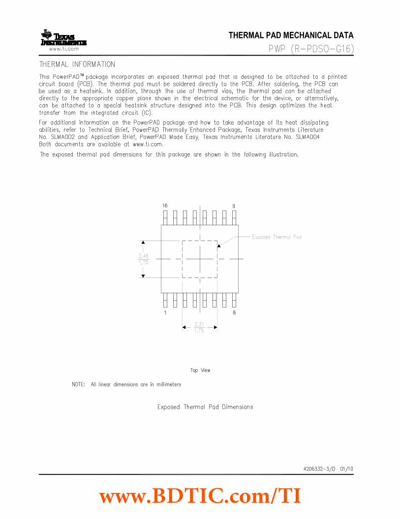
The TPS2838/39/48/49 devices are offered in the thermally enhanced 14-pin and 16-pin PowerPAD TSSOPpackage. The PowerPAD package features an exposed leadframe on the bottom that can be soldered to theprinted-circuit board to improve thermal efficiency. The TPS2838/48 are noninverting control logic while theTPS2839/49 drivers are inverting control logic.
www.BDTIC.com/TI

SLVS367A − MARCH 2001 − REVISED JUNE 2001
3www.ti.com
functional block diagram (TPS2838, TPS2839)
POR
Vr1
PWRRDY THERMALSHUTDOWN
SYS_UVLO
VCC
DRIVEREGULATOR
REFERENCES
VCC
Vr1Vref
0.9 × Vref
VDRVADJ
SHUTDOWN
BOOT
0.9 × Vref
AGND
BOOTLO
HIGHDR
SHUTDOWN
INVERTING OPTIONTPS2839 ONLY
PGND
LOWDR
SYS_UVLO
VDRV
DEADTIMECONTROL DELAY
SYNC
DTENABLE
IN
functional block diagram (TPS2848, TPS2849)
POR
Vr1
PWRRDY THERMALSHUTDOWN
SYS_UVLO
VCC
DRIVEREGULATOR
REFERENCES
VCC
Vr1Vref
0.9 × Vref
VDRV
SHUTDOWN
BOOT
0.9 × Vref
AGND
BOOTLO
HIGHDR
SHUTDOWN
INVERTING OPTIONTPS2849 ONLY
PGND
LOWDR
SYS_UVLO
VDRV
DEADTIMECONTROL DELAY
DTENABLE
IN
www.BDTIC.com/TI

SLVS367A − MARCH 2001 − REVISED JUNE 2001
4 www.ti.com
Terminal Functions
TERMINAL
NAMENO. DESCRIPTION
NAMETPS283x TPS284x
DESCRIPTION
ADJ 6 — Adjust. The adjust pin is the feedback pin for the drive regulator (TPS283X only)
AGND 8 7 Analog ground
BOOT 16 14 Bootstrap. A capacitor is connected between the BOOT and BOOTLO pins to develop the floatingbootstrap voltage for the high-side MOSFET. The capacitor value is typically between 0.1 µF and 1 µF.
BOOTLO 14 12 Boot low. This pin connects to the junction of the high-side and low-side MOSFETs.
DELAY 4 4 Delay. Connecting a capacitor between this pin and ground adjusts the deadtime for high-side driver
DT 7 6 Deadtime control. Connect DT to the junction of the high-side and low-side MOSFETs
ENABLE 1 1 Enable. If ENABLE is low, both drivers are off.
HIGHDR 15 13 High drive. This pin is the output drive for the high-side power MOSFET.
IN 2 2 Input. This pin is the input signal to the MOSFET drivers.
LOWDR 11 9 Low drive. This pin is the output drive for the low-side power MOSFET.
NC 10 5 No internal connection
PGND 9 8 Power ground. This pin is connected to the FET power ground.
PWRRDY 3 3 Power ready. This open-drain pin indicates a power good for VDRV and VCC.
SYNC 5 — Synchronous rectifier enable. If SYNC is low, the low-side driver is always off; if SYNC is high, thelow-side driver provides gate drive to the low-side MOSFET.
VCC 13 11 Input power supply. It is recommended that a capacitor (minimum 1 µF) be connected from VCC toPGND. Note that VCC must be 2 V higher than VDRV.
VDRV 12 10 Drive regulator output voltage. It is recommended that a capacitor (minimum 1 µF) be connected fromVDRV to PGND. Note that VCC must be 2 V higher than VDRV.
detailed description
low-side driver
The low-side driver is designed to drive low rDS(on) N-channel MOSFETs. The current rating of the driver is 4 A,source and sink.
high-side driver
The high-side driver is designed to drive low rDS(on) N-channel MOSFETs. The current rating of the driver is 4 Aminimum, source and sink. The high-side driver can be configured as a GND-reference driver or as afloating-bootstrap driver. The internal bootstrap diode is a Schottky, for improved drive efficiency. The maximumvoltage that can be applied from BOOT to ground is 30 V.
dead-time (DT) control
Dead-time control prevents shoot-through current from flowing through the main power FETs during switchingtransitions by controlling the turnon times of the MOSFET drivers. The high-side driver is not allowed to turnon until the gate drive voltage to the low-side FET is low, and the low-side driver is not allowed to turn on untilthe voltage at the junction of the power FETs (BOOTLO) is low. The TTL-compatible DT terminal connects tothe junction of the power FETs.
ENABLE
The ENABLE terminal enables the drivers. When enable is low, the output drivers are low. ENABLE is aTTL-compatible digital terminal.
www.BDTIC.com/TI

SLVS367A − MARCH 2001 − REVISED JUNE 2001
5www.ti.com
detailed description (continued)
IN
The IN terminal is a TTL-compatible digital terminal that is the input control signal for the drivers. TheTPS2838/48 have noninverting inputs; the TPS2839/49 have inverting inputs. On the TPS2838 and TPS2848,a high on IN results in a high on HIGHDR. On the TPS2839 and TPS2849, a high on IN results in a low onHIGHDR.
SYNC (TPS283x only)
The SYNC terminal controls whether the drivers operate in synchronous or nonsynchronous mode. Insynchronous mode, the low-side FET is operated as a synchronous rectifier. In nonsynchronous mode, thelow-side FET is always off. SYNC is a TTL-compatible digital terminal.
PWRRDY
Depicts the status of the VCC pin voltage and the driver regulator output on the open-drain PWRRDY pin.
DELAY
Adjustable high-side turnon delay from from when the low-side FET is turned off.
ADJ (TPS283x only)
Input for adjusting the driver regulator output. See the application information section for the adjustment formula.
absolute maximum ratings over operating free-air temperature (unless otherwise noted) †
Supply voltage range, VCC (see Note 1) −0.3 V to 16 V. . . . . . . . . . . . . . . . . . . . . . . . . . . . . . . . . . . . . . . . . . . . . . Input voltage range: ADJ −0.3 V to 7 V. . . . . . . . . . . . . . . . . . . . . . . . . . . . . . . . . . . . . . . . . . . . . . . . . . . . . . . . . . . .
BOOT to PGND (high-side driver ON) −0.3 V to 30 V. . . . . . . . . . . . . . . . . . . . . . . . . . . . . . BOOTLO to PGND −0.3 V to 16 V. . . . . . . . . . . . . . . . . . . . . . . . . . . . . . . . . . . . . . . . . . . . . . BOOT to BOOTLO −0.3 V to 16 V. . . . . . . . . . . . . . . . . . . . . . . . . . . . . . . . . . . . . . . . . . . . . . ENABLE, IN, and SYNC −0.3 V to 16 V. . . . . . . . . . . . . . . . . . . . . . . . . . . . . . . . . . . . . . . . . . VDRV, PWRRDY, and DELAY −0.3 V to 16 V. . . . . . . . . . . . . . . . . . . . . . . . . . . . . . . . . . . . . DT −0.3 V to 16 V. . . . . . . . . . . . . . . . . . . . . . . . . . . . . . . . . . . . . . . . . . . . . . . . . . . . . . . . . . . . .
Continuous total power dissipation See Dissipation Rating Table. . . . . . . . . . . . . . . . . . . . . . . . . . . . . . . . . . . . . . Operating virtual junction temperature range, TJ −40°C to 125°C. . . . . . . . . . . . . . . . . . . . . . . . . . . . . . . . . . . . . . Storage temperature range, Tstg −65°C to 150°C. . . . . . . . . . . . . . . . . . . . . . . . . . . . . . . . . . . . . . . . . . . . . . . . . . . . Lead temperature soldering 1,6 mm (1/16 inch) from case for 10 seconds 260°C. . . . . . . . . . . . . . . . . . . . . . .
† Stresses beyond those listed under “absolute maximum ratings” may cause permanent damage to the device. These are stress ratings only, andfunctional operation of the device at these or any other conditions beyond those indicated under “recommended operating conditions” is notimplied. Exposure to absolute-maximum-rated conditions for extended periods may affect device reliability.
NOTE 1: Unless otherwise specified, all voltages are with respect to PGND.
www.BDTIC.com/TI

SLVS367A − MARCH 2001 − REVISED JUNE 2001
6 www.ti.com
DISSIPATION RATING TABLE
PACKAGE TA ≤ 25°C DERATING FACTOR TA = 70°C TA = 85°C
14-pin PWP with solder‡ 2668 26.68 mW/°C 1467 1067
14-pin PWP without solder‡ 1024 10.24 mW/°C 563 409
16-pin PWP with solder‡ 2739 27.39 mW/°C 1506 1095
16-pin PWP without solder‡ 1108 11.08 mW/°C 609 443
JUNCTION-CASE THERMAL RESISTANCE TABLE
14-pin PWP Junction-case thermal resistance 2.07 °C/W
16-pin PWP Junction-case thermal resistance 2.07 °C/W‡ Test Board Conditions:
1. Thickness: 0.0622. 3 × 3 (for packages < 27 mm long)3. 4 × 4 (for packages > 27 mm long)4. 2-oz copper traces located on the top of the board (0,071 mm thick)5. Copper areas located on the top and bottom of the PCB for soldering6. Power and ground planes, 1-oz copper (0,036 mm thick)7. Thermal vias, 0,33 mm diameter, 1,5 mm pitch8. Thermal isolation of power planeFor more information, refer to TI technical brief literature number SLMA002.
recommended operating conditions
MIN NOM MAX UNIT
Supply voltage, VCC 10 15 V
Input voltage, VI BOOT to PGND 10 29 V
electrical characteristics over recommended operating virtual junction temperature range,VCC = 12 V, ENABLE = High, C L = 3.3 nF (unless otherwise noted)
supply currentPARAMETER TEST CONDITIONS MIN TYP MAX UNIT
ICC Quiescent currentV(ENABLE) = Low, VCC = 13 V 425 µA
ICC Quiescent currentV(ENABLE) = High, VCC = 13 V 1 mA
NOTE 2: Ensured by design, not production tested.
www.BDTIC.com/TI

SLVS367A − MARCH 2001 − REVISED JUNE 2001
7www.ti.com
electrical characteristics over recommended operating virtual junction temperature range,VCC = 12 V, ENABLE = High, C L = 3.3 nF (unless otherwise noted) (continued)
dead-time controlPARAMETER TEST CONDITIONS MIN TYP MAX UNIT
VIH(LOWDR) LOWDR high-level input voltage Over full VDRV range See Note 2 50 %VDRV
VIL(LOWDR) LOWDR low-level input voltage Over full VDRV range See Note 2 1 V
VIH(DT) DT high-level input voltage Over full VCC range 2 V
VIL(DT) DT low-level input voltage Over full VCC range 1 V
Deadtime delay V(VDRV) = 4 V to 14 V See Note 2 0.5 1 1.5 ns/pF
Driver nonoverlap time (DT to LOWDR)V(VDRV) = 4.5 V, TJ = 25°C, See Note 2 30 150 ns
Driver nonoverlap time (DT to LOWDR)V(VDRV) = 14.5 V, TJ = 25°C, See Note 2 30 100 ns
Driver nonoverlap time (LOWDR to
V(VDRV) = 4.5 V, CL(Delay) = 50 pFTJ = 25°C, See Note 2
75 180
nsDriver nonoverlap time (LOWDR toHIGHDR) V(VDRV) = 14.5 V, CL(Delay) = 50 pF
TJ = 25°C, See Note 258 125
ns
Driver nonoverlap time (LOWDR to
V(VDRV) = 4.5 V, CL(Delay) = 0 pFTJ = 25°C, See Note 2
50 125
nsDriver nonoverlap time (LOWDR toHIGHDR) V(VDRV) = 14.5 V, CL(Delay) = 0 pF
TJ = 25°C, See Note 230 100
ns
NOTE 2: Ensured by design, not production tested.
high-side driverPARAMETER TEST CONDITIONS MIN TYP MAX UNIT
V(BOOT) −V(BOOTLO) = 4 V, V(HIGHDR) = 0.5 V (src) 1 1.3V(BOOT) −V(BOOTLO) = 4 V,See Note 2 V(HIGHDR) = 4 V (sink) 2 2.4
Peak output currentV(BOOT) −V(BOOTLO) = 8 V, V(HIGHDR) = 0.5 V (src) 2 2.4
APeak output currentV(BOOT) −V(BOOTLO) = 8 V,See Note 2 V(HIGHDR) = 8 V (sink) 2 3.3
A
V(BOOT) −V(BOOTLO) = 14 V, V(HIGHDR) = 0.5 V (src) 2 3.9V(BOOT) −V(BOOTLO) = 14 V,See Note 2 V(HIGHDR) = 14 V (sink) 2 4.4
V(BOOT) −V(BOOTLO) = 4.5 V V(HIGHDR) = 4 V (src) 45V(BOOT) −V(BOOTLO) = 4.5 VTJ = 25°C V(HIGHDR) = 0.5 V (sink) 6
ro Output resistanceV(BOOT) −V(BOOTLO) = 7.5 V, V(HIGHDR) = 7 V (src) 26
Ωro Output resistanceV(BOOT) −V(BOOTLO) = 7.5 V,TJ = 25°C V(HIGHDR) = 0.5 V (sink) 5
Ω
V(BOOT) −V(BOOTLO) = 11.5 V, V(HIGHDR) = 11 V (src) 20V(BOOT) −V(BOOTLO) = 11.5 V,TJ = 25°C V(HIGHDR) = 0.5 V (sink) 4
HIGHDRV-to-BOOTLO resistor 250 kΩ
CL = 3.3 nF, V(BOOTLO) = GND,V(BOOT)= 4 V 85
CL = 3.3 nF, V(BOOTLO) = GND,TJ = 125°C V(BOOT)= 8 V 70
tr/tfRise and fall time
TJ = 125°CV(BOOT)= 14 V 65
nstr/tfRise and fall time (see Notes 2 and 3)
CL = 10 nF, V(BOOTLO) = GND,V(BOOT)= 4 V 170
ns(see Notes 2 and 3)CL = 10 nF, V(BOOTLO) = GND,TJ = 125°C V(BOOT)= 8 V 140TJ = 125°C
V(BOOT)= 14 V 100
Propagation delay time,V(BOOTLO) = GND, TJ = 125°C,
V(BOOT) = 4 V 120
tPHL
Propagation delay time,HIGHDR going low(excluding deadtime)
V(BOOTLO) = GND, TJ = 125°C,See Notes 2 and 3
V(BOOT)= 8 V 100 nstPHL HIGHDR going low(excluding deadtime)
See Notes 2 and 3V(BOOT)= 14 V 80
ns
NOTES: 2: Ensured by design, not production tested.3. The pullup/pulldown circuits of the drivers are bipolar and MOSFET transistors in parallel. The peak output current rating is the
combined current from the bipolar and MOSFET transistors. The output resistance is the rDS(on) of the MOSFET transistor whenthe voltage on the driver output is less than the saturation voltage of the bipolar transistor.
www.BDTIC.com/TI

SLVS367A − MARCH 2001 − REVISED JUNE 2001
8 www.ti.com
electrical characteristics over recommended operating virtual junction temperature range,VCC = 12 V, ENABLE = High, C L = 3.3 nF (unless otherwise noted) (continued)
low-side driverPARAMETER TEST CONDITIONS MIN TYP MAX UNIT
V(VDRV) = 4 V, V(LOWDR) = 0.5 V (src) 1 1.6V(VDRV) = 4 V,TJ = 25°C, See Note 2 V(LOWDR) = 4 V (sink) 2 2.4
Peak output currentV(VDRV) = 8 V, V(HIGHDR) = 0.5 V (src) 2 2.4
APeak output currentV(VDRV) = 8 V,TJ = 25°C, See Note 2 V(HIGHDR) = 8 V (sink) 2 3.3
A
V(VDRV) = 14 V (src), V(HIGHDR) = 0.5 V (src) 2 3.9V(VDRV) = 14 V (src),TJ = 25°C, See Note 2 V(HIGHDR) = 14 V (sink) 2 4.4
V(VDRV) = 4.5 V, V(LOWDR) = 4 V (src) 30V(VDRV) = 4.5 V,TJ = 25°C V(LOWDR) = 0.5 V (sink) 8
ro Output resistanceV(VDRV) = 7.5 V, V(LOWDR) = 7 V (src) 25
Ωro Output resistanceV(VDRV) = 7.5 V,TJ = 25°C V(LOWDR) = 0.5 V (sink) 7
Ω
V(VDRV)= 11.5 V, V(LOWDR) = 11 V (src) 22V(VDRV)= 11.5 V,TJ = 25°C V(LOWDR) = 0.5 V (sink) 6
LOWDR-to-PGND resistor 250 kΩ
CL = 3.3 nF, TJ = 125°C,V(VDRV) = 4 V 60
CL = 3.3 nF, TJ = 125°C,See Note 2
V(VDRV) = 8 V 50
tr/tf Rise and fall time
See Note 2V(VDRV) = 14 V 40
nstr/tf Rise and fall time
CL = 10 nF, TJ = 125°C,V(VDRV) = 4 V 110
ns
CL = 10 nF, TJ = 125°C,See Note 2
V(VDRV) = 8 V 100See Note 2
V(VDRV) = 14 V 80
Propagation delay time, LOWDR TJ = 125°C,V(VDRV) = 4 V 110 ns
tPLHPropagation delay time, LOWDRgoing high (excluding deadtime)
TJ = 125°C,See Notes 2 and 3
V(VDRV) = 8 V 90 nstPLH going high (excluding deadtime) See Notes 2 and 3V(VDRV) = 14 V 80 ns
NOTES: 2: Ensured by design, not production tested.3: The pullup/pulldown circuits of the drivers are bipolar and MOSFET transistors in parallel. The peak output current rating is the
combined current from the bipolar and MOSFET transistors. The output resistance is the rDS(on) of the MOSFET transistor whenthe voltage on the driver output is less than the saturation voltage of the bipolar transistor.
VCC undervoltage lockoutPARAMETER TEST CONDITIONS MIN TYP MAX UNIT
Start threshold voltage 10.3 V
Stop threshold voltage 7.5 V
Vhys Hysteresis voltage 1 1.5 V
tpd Propagation delay time 50-mV overdrive, See Note 2 300 1000 ns
td Falling-edge delay time See Note 2 2 5 usNOTE 2: Ensured by design, not production tested.
www.BDTIC.com/TI

SLVS367A − MARCH 2001 − REVISED JUNE 2001
9www.ti.com
electrical characteristics over recommended operating virtual junction temperature range,VCC = 12 V, ENABLE = High, C L = 3.3 nF (unless otherwise noted) (continued)
digital control (IN, ENABLE, SYNC)PARAMETER TEST CONDITIONS MIN TYP MAX UNIT
VIH High-level input voltageIN Over full VCC range 2 V
VIH High-level input voltageENABLE, SYNC Over full VCC range 2.2 V
VIL Low-level input voltageIN Over full VCC range 1 V
VIL Low-level input voltageENABLE, SYNC Over full VCC range 1 V
ENABLE propagation delay time See Note 2 2 7 µsNOTE 2: Ensured by design, not production tested.
thermal shutdownPARAMETER TEST CONDITIONS MIN TYP MAX UNIT
Thermal shutdown See Note 2 155 170 185 C
td Falling edge delay time See Note 2 10 20 µsNOTE 2: Ensured by design, not production tested.
drive regulatorPARAMETER TEST CONDITIONS MIN TYP MAX UNIT
Recommended output voltage 4 14 V
VO Output voltage VCC = 10 V to 15 V, IO = 5 mA to 150 mA −2 2 %nom
Vref Reference voltage VCC = 10 V to 15 V 1.235 V
Dropout voltageVCC = 10 V, IO = 150 mASee Note 2
1000 1100 mV
Line regulation VCC = 10 V to 15 V, IO = 5 mA 0.2 %/V
Load regulation VCC = 10 V, IO = 5 mA to 150 mA 2 %
Current limit VCC = 8 V 0.5 0.6 A
PWRRDY saturation voltage IO = 5 mA 0.8 V
Ilkg Leakage current VI(PWRRDY) = 4.5 V 1 µA
drive regulator undervoltage lockoutPARAMETER TEST CONDITIONS MIN TYP MAX UNIT
Start threshold voltage See Note 2 85 %Vref
Stop threshold voltage See Note 2 80 %Vref
Vhys Hysteresis voltage See Note 2 2.5 5 %Vref
tpd Propagation delay time 50-mV overdrive, See Note 2 300 1000 ns
Falling-edge delay time See Note 2 2 5 µs
Power on reset time See Note 2 100 1000 µsNOTE 2: Ensured by design, not production tested.
www.BDTIC.com/TI

SLVS367A − MARCH 2001 − REVISED JUNE 2001
10 www.ti.com
PARAMETER MEASUREMENT INFORMATION
tr tf
90% 90%
10%10%
50% 50%
50% 50%
VI(EN, SYNC, IN)
VO(LOWDRV, HIGHDR)
ton toff
50% 50%
50% 50%
ton toff
VI(EN, SYNC, IN)
VO(LOWDRV, HIGHDR)
VO(LOWDRV, HIGHDR)
Rising EdgeFalling Edge
High-Side and Low-Side Drive
Figure 1. Voltage Waveforms
TYPICAL CHARACTERISTICS
Figure 2
04 6 8 10
10
RISE TIMEvs
INPUT VOLTAGE (VDRV)
13
VI − Input Voltage (VDRV) − V
50
60
70
20
30
40
t r−
Ris
e Ti
me
− ns
5 7 9 11 12
CL = 3.3 nFTJ = 25°C
1514
High Side
Low Side
Figure 3
FALL TIMEvs
INPUT VOLTAGE (VDRV)
t f−
Fal
l Tim
e −
ns
04 6 8 10
5
13
VI − Input Voltage (VDRV) − V
25
30
35
10
15
20
5 7 9 11 12 1514
CL = 3.3 nFTJ = 25°C
High Side
Low Side
www.BDTIC.com/TI

SLVS367A − MARCH 2001 − REVISED JUNE 2001
11www.ti.com
TYPICAL CHARACTERISTICS
Figure 4
RISE TIMEvs
JUNCTION TEMPERATURE
t r−
Ris
e Ti
me
− ns
TJ − Junction Temperature − ° C
00 50 100
10
125
50
60
20
30
40
25 75−50 −25
VDRV = 8 VCL = 3.3 nF
High Side
Low Side
Figure 5
FALL TIMEvs
JUNCTION TEMPERATURE
t f−
Fal
l Tim
e −
ns
TJ − Junction Temperature − ° C
00 50 100
5
125
25
30
35
10
15
20
25 75−50 −25
VDRV = 8 VCL = 3.3 nF
High Side
Low Side
Figure 6
04 6 8 10
20
LOW-TO-HIGH PROPAGATION DELAY TIMEvs
INPUT VOLTAGE (VDRV)
13
VI − Input Voltage (VDRV) − V
100
120
140
40
60
80
5 7 9 11 12
200
160
180
t PLH
− Lo
w-t
o-H
igh
Pro
paga
tion
Del
ay T
ime
− ns
1514
CL = 3.3 nFTJ = 25°C
Low Side
High Side
Figure 7
HIGH-TO-LOW PROPAGATION DELAY TIMEvs
INPUT VOLTAGE (VDRV)
VI − Input Voltage (VDRV) − V
04 6 8 10
20
13
100
120
140
40
60
80
5 7 9 11 12
t PH
L−
Hig
h-to
-Low
Pro
paga
tion
Del
ay T
ime
− ns CL = 3.3 nF
TJ = 25°C
1514
High Side
Low Side
www.BDTIC.com/TI

SLVS367A − MARCH 2001 − REVISED JUNE 2001
12 www.ti.com
TYPICAL CHARACTERISTICS
Figure 8
LOW-TO-HIGH PROPAGATION DELAY TIMEvs
JUNCTION TEMPERATURE
TJ − Junction Temperature − ° C
00 50 100
20
125
100
120
140
40
60
80
25 75
160
180
t PLH
− Lo
w-t
o-H
igh
Pro
paga
tion
Del
ay T
ime
− ns
−25−50
VDRV = 8 VCL = 3.3 nF
High Side
Low Side
Figure 9
HIGH-TO-LOW PROPAGATION DELAY TIMEvs
JUNCTION TEMPERATURE
TJ − Junction Temperature − ° C
00 50 100
10
125
50
60
70
20
30
40
25 75
80
t PH
L−
Hig
h-to
-Low
Pro
paga
tion
Del
ay T
ime
− ns
−25−50
VDRV = 8 VCL = 3.3 nF
High Side
Low Side
Figure 10
DRIVER-OUTPUT RISE TIMEvs
LOAD CAPACITANCE
CL − Load Capacitance − nF
t r−
Driv
er-O
utpu
t Ris
e Ti
me
− ns
100
10
1
1000
0.01 1 10 1000.1
VDRV = 8 VTJ = 25°C
Low Side
High Side
Figure 11
DRIVER-OUTPUT FALL TIMEvs
LOAD CAPACITANCE
CL − Load Capacitance − nF
t f−
Driv
er-O
utpu
t Fal
l Tim
e −
ns
100
10
1
1000
0.01 1 10 1000.1
VDRV = 8 VTJ = 25°C
Low Side
High Side
www.BDTIC.com/TI

SLVS367A − MARCH 2001 − REVISED JUNE 2001
13www.ti.com
TYPICAL CHARACTERISTICS
Figure 12
SUPPLY CURRENTvs
INPUT VOLTAGE (VDRV)
VI − Input Voltage (VDRV) − V
0
1
10
7
8
9
2
3
5
CC
IS
uppl
y C
urre
nt −
mA
−
4
6
4 6 8 10 135 7 9 11 12 1514
CL = 50 pFTJ = 25°C
50 kHz25 kHz
300 kHz
200 kHz
100 kHz500 kHz
Figure 13
SUPPLY CURRENTvs
INPUT VOLTAGE (VDRV)
VI − Input Voltage (VDRV) − V
0
2.5
25
17.5
20
22.5
5
7.5
12.5
CC
IS
uppl
y C
urre
nt −
mA
−
10
15
4 6 8 10 135 7 9 11 12 1514
CL = 50 pFTJ = 25°C
1 MHz
2 MHz
Figure 14
PEAK SOURCE CURRENTvs
INPUT VOLTAGE (VDRV)
Pea
k S
ourc
e C
urre
nt −
A
VI − Input Voltage (VDRV) − V
0
0.5
4
2.5
3
3.5
1
1.5
2
4.5
4 6 8 10 135 7 9 11 12 1514
TJ = 25°C
High Side
Low Side
Figure 15
Pea
k S
ink
Cur
rent
− A
PEAK SINK CURRENTvs
INPUT VOLTAGE (VDRV)
VI − Input Voltage (VDRV) − V
0
0.5
4
2.5
3
3.5
1
1.5
2
4.5
4 6 8 10 135 7 9 11 12 1514
5
TJ = 25°C
High Side
Low Side
www.BDTIC.com/TI

SLVS367A − MARCH 2001 − REVISED JUNE 2001
14 www.ti.com
TYPICAL CHARACTERISTICS
Figure 16
START/STOP VCC UNDERVOLTAGE LOCKOUTvs
JUNCTION TEMPERATURE
TJ − Junction Temperature − ° C
8.20 50 100
8.4
125
9.2
9.4
9.6
8.6
8.8
9
25 75
9.8
10
Sta
rt/S
top
−25−50
Start
Stop
V CC
Und
ervo
ltage
Loc
kout
− V
Figure 17
VO − Output Voltage − V
0
200
400
600
1000
800
1200
0 0.5 1 1.50.25 0.75 1.25 1.75 2
BOOTSTRAP SCHOTTKY DIODEINPUT CURRENT
vsOUTPUT VOLTAGE
II
− B
oots
trap
Sch
ottk
y D
iode
Inpu
t Cur
rent
− m
A
TJ = 25°C
Figure 18
04 6 8 10
20
DELAY TIME (DEAD TIME)vs
INPUT VOLTAGE (VDRV)
13
VI − Input Voltage (VDRV) − V
100
120
140
40
60
80
5 7 9 11 12
200
160
180
Dea
ly T
ime
(Dea
d Ti
me)
− n
s
1514
50 pF20 pF10 pF5 pF
1 pF0 pF
TJ = 25°C
Figure 19
DELAY TIMEvs
JUNCTION TEMPERATURE
TJ − Junction Temperature − ° C
00 50 100
20
125
100
120
140
40
60
80
25 75
160
180
Del
ay T
ime
− ns
−25−50
200
50 pF
5 pF
1 pF0 pF
50 pF20 pF10 pF
VDRV = 8 V
www.BDTIC.com/TI

VDRV
ADJ
R2
R1
SLVS367A − MARCH 2001 − REVISED JUNE 2001
15www.ti.com
TYPICAL CHARACTERISTICS
Figure 20
VDRV LINE REGULATION
VCC − Supply Voltage − V
8.055
8.056
8.06
8.061
8.062
8.057
8.058
8.059
10 1311 12 1514
CL(VDRV) = 1 µFTJ = 25°C
− O
utpu
t Vol
tage
− V
VO
Figure 21
VDRV LOAD REGULATION
II − Input Current − mA
8.085
8.09
8.11
8.115
8.095
8.1
8.105
−10 5010 30 9070 110 150130
CL(VDRV) = 1 µFTJ = 25°C
− O
utpu
t Vol
tage
− V
VO
APPLICATION INFORMATION
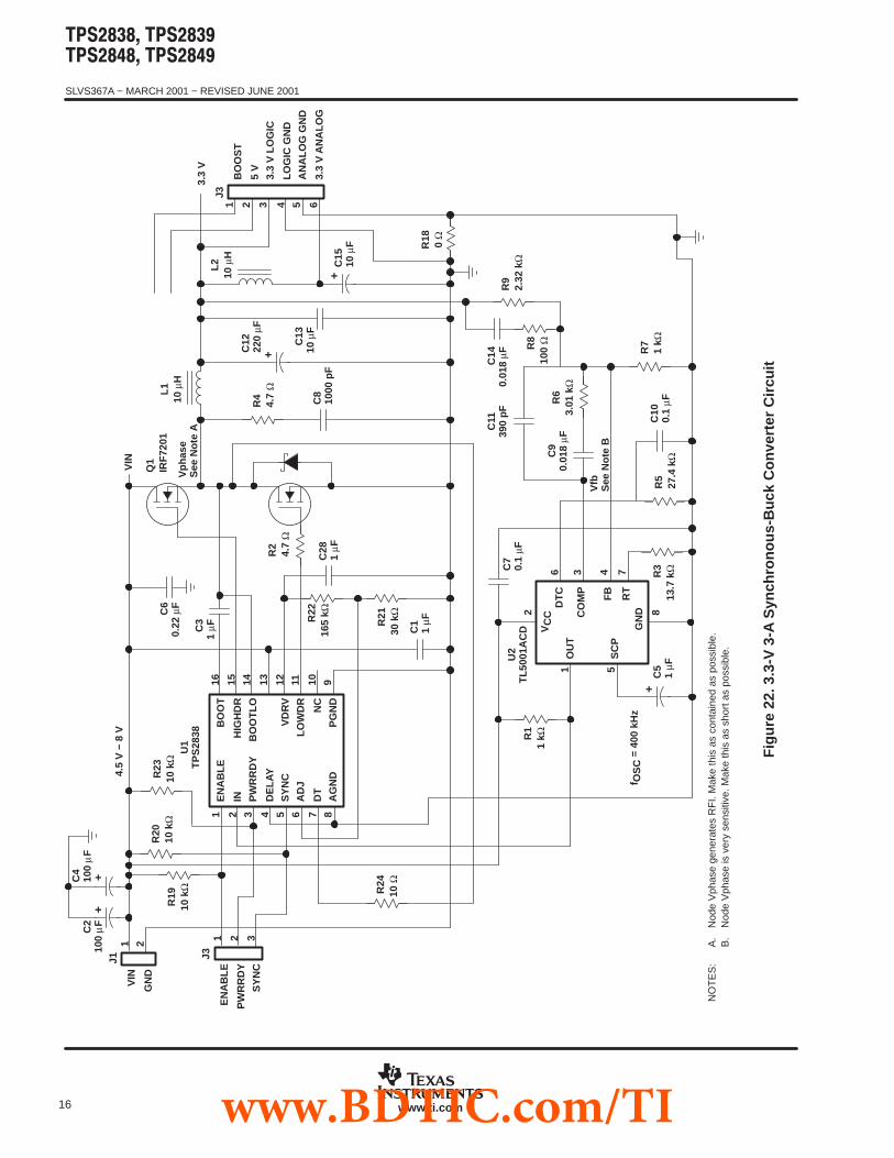
Figure 22 shows the circuit schematic of a 100-kHz synchronous-buck converter implemented with a TL5001ACDpulse-width-modulation (PWM) controller and a TPS2838 driver. The converter operates over an input range from4.5 V to 12 V and has a 3.3-V output. The circuit can supply 3-A continuous load. The converter achieves an efficiencyof 94% for VIN = 5 V, IL=1 A, and 93% for VIN = 5 V, IL = 3 A.
R1(kΩ)
R2(kΩ)
VDRVVoltage
(V)
30 67 4
30 91 5
30 165 8
30 261 12
30 322 14.5
To set the regulator voltage (TPS2838/39) use the following equation:
R2 R11.235
VDRV R1
www.BDTIC.com/TI
SLVS367A − MARCH 2001 − REVISED JUNE 2001
16 www.ti.com
VIN
GN
D
EN
AB
LE
PW
RR
DY
SY
NC
BO
OT
HIG
HD
R
BO
OT
LO
VD
RV
LOW
DR
NC
PG
ND
U1
TP
S28
38
J1 J3E
NA
BLE
IN PW
RR
DY
DE
LAY
SY
NC
AD
J
DT
AG
ND
16 15 14 13 12 11 10 9
1 2 3 4 5 6 7 8
C2
100
µF+
+C4
100
µF
R19
10 k
Ω
R20
10 k
ΩR
2310
kΩ
C6
0.22
µF
Q1
IRF
7201
VIN
C3
1 µF
Vph
ase
See
Not
e A
L210
µH
L110
µH
BO
OS
T
5 V
3.3
V L
OG
IC
J3
LOG
IC G
ND
AN
ALO
G G
ND
3.3
V A
NA
LOG
3.3
V
+C
1510
µF
C13
10 µ
F
+C12
220
µFR
24.
7 Ω
R4
4.7
Ω
C8
1000
pF
C28
1 µF
C1
1 µFR
2216
5 kΩ
R21
30 k
ΩR
2410
Ω
VC
C
FB
CO
MP
DT
C
GN
D
OU
T
SC
P
1
2
5
8
6 3 4
RT
7C7
0.1
µFU
2T
L500
1AC
DR
11
kΩ
+C
51
µFR
313
.7 k
Ω
f OS
C =
400
kH
z
R18
0 Ω
R5
27.4
kΩC
90.
018
µFR
63.
01 k
Ω
R7
1 kΩ
R9
2.32
kΩ
C14
0.01
8 µF
R8
100
Ω
C11
390
pF
4.5
V −
8 V
1 2 1 2 3
C10
0.1
µF
1 2 3 4 5 6
Vfb
See
Not
e B
NO
TE
S:
A.
Nod
e V
phas
e ge
nera
tes
RF
I. M
ake
this
as
cont
aine
d as
pos
sibl
e.B
.N
ode
Vph
ase
is v
ery
sens
itive
. Mak
e th
is a
s sh
ort a
s po
ssib
le.
Fig
ure
22. 3
.3-V
3-A
Syn
chro
nous
-Buc
k C
onve
rter
Circ
uit
www.BDTIC.com/TI

SLVS367A − MARCH 2001 − REVISED JUNE 2001
17www.ti.com
APPLICATION INFORMATION
Great care should be taken when laying out the PC board. The power-processing section is the most criticaland will generate large amounts of EMI if not properly configured. The junction of Q1, Q2, and L1 should be verytight. The connection from Q1 drain to the positive sides of C5, C10, and C11 and the connection from Q2 sourceto the negative sides of C5, C10, and C11 should be as short as possible. The negative terminals of C7 andC12 should also be connected to Q2 source.
Next, the traces from the MOSFET driver to the power switches should be considered. The BOOTLO signal fromthe junction of Q1 and Q2 carries the large gate drive current pulses and should be as heavy as the gate drivetraces. The bypass capacitor (C14) should be tied directly across VCC and PGND.
The next most sensitive node is the FB node on the controller (terminal 4 on the TL5001A). This node is verysensitive to noise pickup and should be isolated from the high-current power stage and be as short as possible.The ground around the controller and low-level circuitry should be tied to the power ground as the output. If thesethree areas are properly laid out, the rest of the circuit should not have other EMI problems and the power supplywill be relatively free of noise.
www.BDTIC.com/TI

PACKAGING INFORMATION
Orderable Device Status (1) PackageType
PackageDrawing
Pins PackageQty
Eco Plan (2) Lead/Ball Finish MSL Peak Temp (3)
TPS2838PWP ACTIVE HTSSOP PWP 16 90 Green (RoHS &no Sb/Br)
CU NIPDAU Level-2-260C-1 YEAR
TPS2838PWPG4 ACTIVE HTSSOP PWP 16 90 Green (RoHS &no Sb/Br)
CU NIPDAU Level-2-260C-1 YEAR
TPS2839PWP ACTIVE HTSSOP PWP 16 90 Green (RoHS &no Sb/Br)
CU NIPDAU Level-2-260C-1 YEAR
TPS2839PWPG4 ACTIVE HTSSOP PWP 16 90 Green (RoHS &no Sb/Br)
CU NIPDAU Level-2-260C-1 YEAR
TPS2848PWP ACTIVE HTSSOP PWP 14 90 Green (RoHS &no Sb/Br)
CU NIPDAU Level-2-260C-1 YEAR
TPS2848PWPG4 ACTIVE HTSSOP PWP 14 90 Green (RoHS &no Sb/Br)
CU NIPDAU Level-2-260C-1 YEAR
TPS2849PWP ACTIVE HTSSOP PWP 14 90 Green (RoHS &no Sb/Br)
CU NIPDAU Level-2-260C-1 YEAR
TPS2849PWPG4 ACTIVE HTSSOP PWP 14 90 Green (RoHS &no Sb/Br)
CU NIPDAU Level-2-260C-1 YEAR
(1) The marketing status values are defined as follows:ACTIVE: Product device recommended for new designs.LIFEBUY: TI has announced that the device will be discontinued, and a lifetime-buy period is in effect.NRND: Not recommended for new designs. Device is in production to support existing customers, but TI does not recommend using this part ina new design.PREVIEW: Device has been announced but is not in production. Samples may or may not be available.OBSOLETE: TI has discontinued the production of the device.
(2) Eco Plan - The planned eco-friendly classification: Pb-Free (RoHS), Pb-Free (RoHS Exempt), or Green (RoHS & no Sb/Br) - please checkhttp://www.ti.com/productcontent for the latest availability information and additional product content details.TBD: The Pb-Free/Green conversion plan has not been defined.Pb-Free (RoHS): TI's terms "Lead-Free" or "Pb-Free" mean semiconductor products that are compatible with the current RoHS requirementsfor all 6 substances, including the requirement that lead not exceed 0.1% by weight in homogeneous materials. Where designed to be solderedat high temperatures, TI Pb-Free products are suitable for use in specified lead-free processes.Pb-Free (RoHS Exempt): This component has a RoHS exemption for either 1) lead-based flip-chip solder bumps used between the die andpackage, or 2) lead-based die adhesive used between the die and leadframe. The component is otherwise considered Pb-Free (RoHScompatible) as defined above.Green (RoHS & no Sb/Br): TI defines "Green" to mean Pb-Free (RoHS compatible), and free of Bromine (Br) and Antimony (Sb) based flameretardants (Br or Sb do not exceed 0.1% by weight in homogeneous material)
(3) MSL, Peak Temp. -- The Moisture Sensitivity Level rating according to the JEDEC industry standard classifications, and peak soldertemperature.
Important Information and Disclaimer:The information provided on this page represents TI's knowledge and belief as of the date that it isprovided. TI bases its knowledge and belief on information provided by third parties, and makes no representation or warranty as to theaccuracy of such information. Efforts are underway to better integrate information from third parties. TI has taken and continues to takereasonable steps to provide representative and accurate information but may not have conducted destructive testing or chemical analysis onincoming materials and chemicals. TI and TI suppliers consider certain information to be proprietary, and thus CAS numbers and other limitedinformation may not be available for release.
In no event shall TI's liability arising out of such information exceed the total purchase price of the TI part(s) at issue in this document sold by TIto Customer on an annual basis.
PACKAGE OPTION ADDENDUM
www.ti.com 28-Aug-2008
Addendum-Page 1
www.BDTIC.com/TI
www.BDTIC.com/TI

www.BDTIC.com/TI

www.BDTIC.com/TI
www.BDTIC.com/TI

www.BDTIC.com/TI

IMPORTANT NOTICE
Texas Instruments Incorporated and its subsidiaries (TI) reserve the right to make corrections, modifications, enhancements, improvements,and other changes to its products and services at any time and to discontinue any product or service without notice. Customers shouldobtain the latest relevant information before placing orders and should verify that such information is current and complete. All products aresold subject to TI’s terms and conditions of sale supplied at the time of order acknowledgment.
TI warrants performance of its hardware products to the specifications applicable at the time of sale in accordance with TI’s standardwarranty. Testing and other quality control techniques are used to the extent TI deems necessary to support this warranty. Except wheremandated by government requirements, testing of all parameters of each product is not necessarily performed.
TI assumes no liability for applications assistance or customer product design. Customers are responsible for their products andapplications using TI components. To minimize the risks associated with customer products and applications, customers should provideadequate design and operating safeguards.
TI does not warrant or represent that any license, either express or implied, is granted under any TI patent right, copyright, mask work right,or other TI intellectual property right relating to any combination, machine, or process in which TI products or services are used. Informationpublished by TI regarding third-party products or services does not constitute a license from TI to use such products or services or awarranty or endorsement thereof. Use of such information may require a license from a third party under the patents or other intellectualproperty of the third party, or a license from TI under the patents or other intellectual property of TI.
Reproduction of TI information in TI data books or data sheets is permissible only if reproduction is without alteration and is accompaniedby all associated warranties, conditions, limitations, and notices. Reproduction of this information with alteration is an unfair and deceptivebusiness practice. TI is not responsible or liable for such altered documentation. Information of third parties may be subject to additionalrestrictions.
Resale of TI products or services with statements different from or beyond the parameters stated by TI for that product or service voids allexpress and any implied warranties for the associated TI product or service and is an unfair and deceptive business practice. TI is notresponsible or liable for any such statements.
TI products are not authorized for use in safety-critical applications (such as life support) where a failure of the TI product would reasonablybe expected to cause severe personal injury or death, unless officers of the parties have executed an agreement specifically governingsuch use. Buyers represent that they have all necessary expertise in the safety and regulatory ramifications of their applications, andacknowledge and agree that they are solely responsible for all legal, regulatory and safety-related requirements concerning their productsand any use of TI products in such safety-critical applications, notwithstanding any applications-related information or support that may beprovided by TI. Further, Buyers must fully indemnify TI and its representatives against any damages arising out of the use of TI products insuch safety-critical applications.
TI products are neither designed nor intended for use in military/aerospace applications or environments unless the TI products arespecifically designated by TI as military-grade or "enhanced plastic." Only products designated by TI as military-grade meet militaryspecifications. Buyers acknowledge and agree that any such use of TI products which TI has not designated as military-grade is solely atthe Buyer's risk, and that they are solely responsible for compliance with all legal and regulatory requirements in connection with such use.
TI products are neither designed nor intended for use in automotive applications or environments unless the specific TI products aredesignated by TI as compliant with ISO/TS 16949 requirements. Buyers acknowledge and agree that, if they use any non-designatedproducts in automotive applications, TI will not be responsible for any failure to meet such requirements.
Following are URLs where you can obtain information on other Texas Instruments products and application solutions:
Products Applications
Amplifiers amplifier.ti.com Audio www.ti.com/audio
Data Converters dataconverter.ti.com Automotive www.ti.com/automotive
DLP® Products www.dlp.com Communications and www.ti.com/communicationsTelecom
DSP dsp.ti.com Computers and www.ti.com/computersPeripherals
Clocks and Timers www.ti.com/clocks Consumer Electronics www.ti.com/consumer-apps
Interface interface.ti.com Energy www.ti.com/energy
Logic logic.ti.com Industrial www.ti.com/industrial
Power Mgmt power.ti.com Medical www.ti.com/medical
Microcontrollers microcontroller.ti.com Security www.ti.com/security
RFID www.ti-rfid.com Space, Avionics & www.ti.com/space-avionics-defenseDefense
RF/IF and ZigBee® Solutions www.ti.com/lprf Video and Imaging www.ti.com/video
Wireless www.ti.com/wireless-apps
Mailing Address: Texas Instruments, Post Office Box 655303, Dallas, Texas 75265Copyright © 2010, Texas Instruments Incorporated
www.BDTIC.com/TI