Embed Size (px)
Citation preview
VIN
RSET
TPS92411
RSNS
DRAIN
VS
VIN
RSET
TPS92411
RSNS
DRAIN
VS
VIN
RSET
TPS92411
RSNS
DRAIN
VS
± +
120 VRMS
VIN
MULT
VREF
ADIM
TSNS
VCC COMP GND
CDD
DOV
CS
CPS
GDL
RCS
TPS92410
Product
Folder
Sample &Buy
Technical
Documents
Tools &
Software
Support &Community
TPS92410SLUSBW9 –MAY 2014
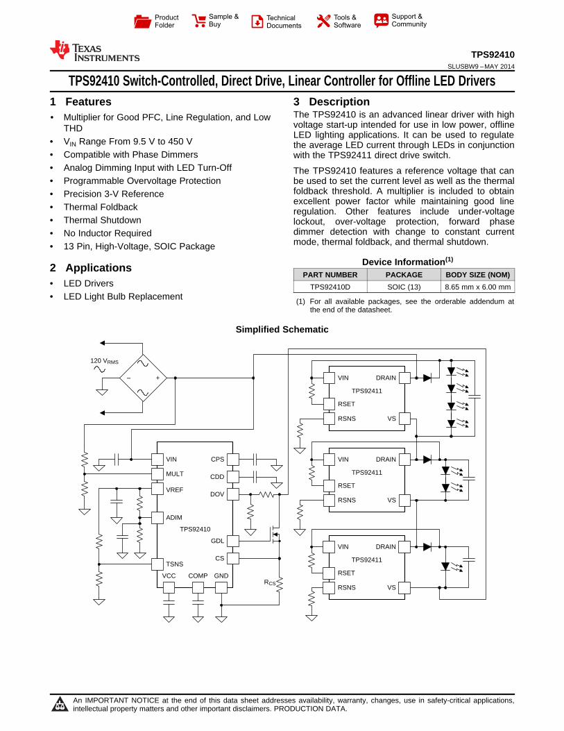
TPS92410 Switch-Controlled, Direct Drive, Linear Controller for Offline LED Drivers1 Features 3 Description
The TPS92410 is an advanced linear driver with high1• Multiplier for Good PFC, Line Regulation, and Low
voltage start-up intended for use in low power, offlineTHDLED lighting applications. It can be used to regulate
• VIN Range From 9.5 V to 450 V the average LED current through LEDs in conjunction• Compatible with Phase Dimmers with the TPS92411 direct drive switch.• Analog Dimming Input with LED Turn-Off The TPS92410 features a reference voltage that can• Programmable Overvoltage Protection be used to set the current level as well as the thermal
foldback threshold. A multiplier is included to obtain• Precision 3-V Referenceexcellent power factor while maintaining good line• Thermal Foldback regulation. Other features include under-voltage
• Thermal Shutdown lockout, over-voltage protection, forward phasedimmer detection with change to constant current• No Inductor Requiredmode, thermal foldback, and thermal shutdown.• 13 Pin, High-Voltage, SOIC Package
Device Information(1)2 Applications
PART NUMBER PACKAGE BODY SIZE (NOM)• LED Drivers TPS92410D SOIC (13) 8.65 mm x 6.00 mm• LED Light Bulb Replacement (1) For all available packages, see the orderable addendum at
the end of the datasheet.
Simplified Schematic
1
An IMPORTANT NOTICE at the end of this data sheet addresses availability, warranty, changes, use in safety-critical applications,intellectual property matters and other important disclaimers. PRODUCTION DATA.

TPS92410SLUSBW9 –MAY 2014 www.ti.com
Table of Contents7.3 Feature Description................................................. 101 Features .................................................................. 17.4 Device Functional Modes........................................ 132 Applications ........................................................... 1
8 Application and Implementation ........................ 133 Description ............................................................. 18.1 Application Information............................................ 134 Revision History..................................................... 28.2 Typical Application ................................................. 145 Pin Configuration and Functions ......................... 3
9 Power Supply Recommendations ...................... 186 Specifications......................................................... 410 Layout................................................................... 186.1 Absolute Maximum Ratings ...................................... 4
10.1 Layout Guidelines ................................................. 186.2 Handling Ratings ...................................................... 410.2 Layout Example .................................................... 186.3 Recommended Operating Conditions....................... 4
11 Device and Documentation Support ................. 196.4 Thermal Information .................................................. 411.1 Trademarks ........................................................... 196.5 Electrical Characteristics........................................... 511.2 Electrostatic Discharge Caution............................ 196.6 Typical Characteristics .............................................. 711.3 Glossary ................................................................ 197 Detailed Description .............................................. 9
12 Mechanical, Packaging, and Orderable7.1 Overview ................................................................... 9Information ........................................................... 207.2 Functional Block Diagram ......................................... 9
4 Revision History
DATE REVISION NOTESJune 2014 * Initial release.
2 Submit Documentation Feedback Copyright © 2014, Texas Instruments Incorporated
Product Folder Links: TPS92410

1
2
3
4
5
6
7
14
13
12
11
10
9
8
VCC
MULT
TSNS
CPS
CDD
DOV
GDL
CS
GND
COMP
ADIM
VREF
VIN
TPS92410www.ti.com SLUSBW9 –MAY 2014
5 Pin Configuration and Functions
SOIC HV13 PIN
(TOP VIEW)
Pin FunctionsPIN
TYPE (1) DESCRIPTIONNAME NO.
Analog input used to set the reference of the linear controller. A 0-V to 1.5-V signal on ADIM sets the currentADIM 9 I sense reference level.A capacitor to ground sets the time interval for dimmer detection. Tie to GND if no phase dimmer operationCDD 2 I/O is required.
COMP 7 I/O Compensation for control loop. Connect a capacitor from the COMP pin to ground.A capacitor to ground sets the length of the CDD pin charge pulse. Leave open if no phase dimmerCPS 1 I/O operation is required.
CS 5 I Current sense input used for linear regulator.Input to monitor linear MOSFET drain voltage. A resistor divider from the DOV pin to the drain connection ofDOV 3 I the MOSFET monitors MOSFET over-voltage. Add a capacitor to GND for filtering.
GDL 4 O Gate drive for an external linear MOSFET.GND 6 G Chip ground return.MULT 11 I AC input to the multiplier. Tap a resistor divider off the rectified line to this pin.TSNS 8 I Thermal sense input. Connect to a resistor and NTC thermistor for thermal foldback.VCC 12 I/O Pre-regulated voltage. Connect a bypass capacitor to ground.VIN 14 P High voltage input. Provides power to the device.VREF 10 O 3-V voltage supply reference. Source used for TSNS input.
(1) I = Input, O = Output, P = Supply, G = Ground
Copyright © 2014, Texas Instruments Incorporated Submit Documentation Feedback 3
Product Folder Links: TPS92410
TPS92410SLUSBW9 –MAY 2014 www.ti.com
6 Specifications
6.1 Absolute Maximum Ratingsover operating free-air temperature range (unless otherwise noted) (1)
MIN MAX UNITInput voltage VIN –0.3 700 V
VCC –0.3 18GDL –0.3 18
Output voltage VMULT, VREF, ADIM, COMP, CPS, CDD, TSNS –0.3 7.7DOV –0.3 6
Source current CS 1 mASink current CS 1 mAOperating junction temperature, TJ
(2) –40 150 °C
(1) Stresses beyond those listed under Absolute Maximum Ratings may cause permanent damage to the device. These are stress ratingsonly, which do not imply functional operation of the device at these or any other conditions beyond those indicated under RecommendedOperating Conditions. Exposure to absolute-maximum-rated conditions for extended periods may affect device reliability.
(2) Maximum junction temperature is internally limited by the device.
6.2 Handling RatingsMIN MAX UNIT
Tstg Storage temperature range –65 150 °CHuman body model (HBM), per ANSI/ESDA/JEDEC JS-001, all pins (2) –1 1 kV
V(ESD)(1) Electrostatic discharge Charged device model (CDM), per JEDEC specification JESD22-C101, –250 250 Vall pins (3)
(1) Electrostatic discharge (ESD) to measure device sensitivity and immunity to damage caused by assembly line electrostatic dischargesinto the device.
(2) Level listed above is the passing level per ANSI/ESDA/JEDEC JS-001. JEDEC document JEP155 states that 500V HBM allows safemanufacturing with a standard ESD control process. Terminals listed as 1000V may actually have higher performance.
(3) Level listed above is the passing level per EIA-JEDEC JESD22-C101. JEDEC document JEP157 states that 250V CDM allows safemanufacturing with a standard ESD control process. Terminals listed as 250V may actually have higher performance.
6.3 Recommended Operating Conditionsover operating free-air temperature range (unless otherwise noted)
MIN NOM MAX UNITVIN Input voltage 9.5 450 VVMULT Multiplier peak input voltage 3 VVADIM Analog dimming input voltage 0 3 VTJ Operating junction temperature -40 125 °C
6.4 Thermal InformationTPS92410
THERMAL METRIC (1) UNITD (13)
RθJA Junction-to-ambient thermal resistance 84.8RθJC(top) Junction-to-case (top) thermal resistance 39.8RθJB Junction-to-board thermal resistance 39.5
°C/WψJT Junction-to-top characterization parameter 8.9ψJB Junction-to-board characterization parameter 39.0RθJC(bot) Junction-to-case (bottom) thermal resistance N/A
(1) For more information about traditional and new thermal metrics, see the IC Package Thermal Metrics application report, SPRA953.
4 Submit Documentation Feedback Copyright © 2014, Texas Instruments Incorporated
Product Folder Links: TPS92410
TPS92410www.ti.com SLUSBW9 –MAY 2014
6.5 Electrical Characteristics–40°C ≤ TJ ≤ 125°C, VVIN = 100 V, VADIM = VMULT = 1 V (unless otherwise noted)
PARAMETER TEST CONDITIONS MIN TYP MAX UNITSUPPLY VOLTAGE (VIN)VCC Pre-regulator output voltage 10.15 V
Rising threshold, VVIN = VVCC 8 8.3VCCUVLO Supply votlage undervoltage protection Falling threshold, VVIN = VVCC 5 5.85 V
Hysteresis 2.15IVIN Input voltage bias current VVCC = 12 V 2.5 50 μAIVCC Supply bias current 305 500
μASupply standby current VVIN = 0 V, VVCC = 7 V (UVLO) 145
IVCCLIM VCC supply current limit VVCC = 7.5 V 8 25 mAVVCC stepped from 6.075 V to 110% ofTplh(UVLO) VCC supply glitch filter rising 16.2 μsVCCUVLO,rising
MULTIPLIER (MULT)VMULT,LINEAR Multiplier linear range 0 3.5 VVCOMP,LINEAR COMP pin linear range 1.5 3.25 VRMULT Input impedance 500 580 700 kΩ
VMULT = 1.5 V, VCOMP = 2.25 V,AMULT Multiplier gain 0.95 1.43 1.85 1/Vk = VMULT_OUT/[(VCOMP–1.5 V) ×
VMULT]VMULT,OFFSET Multiplier output offset VMULT = 0 V, VCOMP = 2.25 V 13.7 mV
VADIM = VTSNS = open; VCOMP = 4 V,MULTOUT,mx Multiplier Output Clamp Voltage 2.25 2.43 2.65 VVMULT = 3.5 VVOLTAGE REFERENCE (VREF)VVREF Reference voltage IVREF = 100 μA 2.85 3 3.15 VVREFLINE Line regulation 8.5 V ≤ VVIN ≤ 100 V 1%VREFLOAD Load regulation 10 μA ≤ IREF ≤ 200 μA 1%TRANSCONDUCTANCE AMPLIFIER (ADIM, COMP)ADIMLIM ADIM operating voltage limit 1.425 1.5 1.575 VIADIM Pull-up current 0.5 1 μAADIMSD ADIM linear shutdown threshold Falling 18 40 70 mVADIMSD,HYS ADIM shutdown hysteresis 20 mVgM Transconductance 43.3 μSVOFFSET Input offset voltage VADIM = 0.5 V -20 20 mV
VCOMP = 2.25 V, VMULT = 0V,IOUT,SOURCE Output source current 65VADIM = VTSNS = 2 VμAIOUT,SINK Output sink current VCOMP = 2.25 V, VTSNS = 0 V 75
ISTART VCOMP = 0 V, VADIM = 0 V 485DIMMER DETECT (MULT, CPS, CDD)ICPS Charge current for CPS pin 6.7 10 13.3ICDD,c Charge current for CDD pin 5.7 10 13.3 μAICDD,d Discharge current for CDD pin 0.67 1 1.33
VMULT stepped from 0 V to 1 V,Dv/Dt Maximum detection threshold 1/100 V/μsminimum slew rate requiredVOFFSET Detector offset voltage 0.41VTH,CDD CDD threshold 1.5 VVTH,CPS CPS threshold 1.5RCSP Pull down RDS(on) 314 Ω
Copyright © 2014, Texas Instruments Incorporated Submit Documentation Feedback 5
Product Folder Links: TPS92410
TPS92410SLUSBW9 –MAY 2014 www.ti.com
Electrical Characteristics (continued)–40°C ≤ TJ ≤ 125°C, VVIN = 100 V, VADIM = VMULT = 1 V (unless otherwise noted)
PARAMETER TEST CONDITIONS MIN TYP MAX UNITDRAIN OVER-VOLTAGE (DOV)VTH,DOV Drain over-voltage threshold 1.38 1.5 1.62 VVHYS,DOV Internal DOV hysteresis 20 mV
VDOV = 1.5 V, Device in over-voltageIHYS,DOV Drain over-voltage source current 0.7 1 1.5 μAmodeLinear CS reference during over-VREF,DOV VDOV = 1.75 V 0.1 Vvoltage
THERMAL FOLDBACK (TSNS)TSNSLIM TSNS operating voltage limit 1.425 1.5 1.575 V
VADIM = VTSNS = 1 V, Measure 2.1reference to the linear error amplifiermV
VTSNS = 0 V, Measure reference to the 3.6linear error amplifierITSNS Pull-up current 0.5 1 µALINEAR CURRENT SENSE (CS)VCS(max) CS voltage level (CC dimming mode) 2.5 V = VADIM = VTSNS 1.425 1.5 1.575
VVCS(max) CS voltage level (PFC mode) 2.5 V = VADIM = VTSNS 1.125 1.291 1.425VIO Input offset voltage VREF = 1 V –17 2.57 17 mVVCMR– Minimum input common mode range 0 VGATE DRIVER (GDL)VOH High-level output voltage, GDL ILOAD = –1 mA 6.5 8.2
VVOL Low-level output voltage, GDL ILOAD = 1 mA 0.152 0.45IOUT(src) Output source current VGDL= 4 V 2.5 8.1
mAIOUT(snk) Output sink current VGDL= 4 V 2.5 11.9THERMAL SHUTDOWNTSD Thermal shutdown 175
°CThermal shutdown hysteresis 10
6 Submit Documentation Feedback Copyright © 2014, Texas Instruments Incorporated
Product Folder Links: TPS92410

0
10
20
30
40
50
60
0.0 0.2 0.4 0.6 0.8 1.0 1.2 1.4
Inpu
t C
urre
nt (
mA
)
TSNS Voltage (V) C011
0
10
20
30
40
50
60
0.0 0.2 0.4 0.6 0.8 1.0 1.2 1.4
Inpu
t C
urre
nt (
mA
)
TSNS Voltage (V) C012
0
10
20
30
40
50
60
0.0 0.2 0.4 0.6 0.8 1.0 1.2 1.4
Inpu
t C
urre
nt (
mA
)
ADIM Voltage (V) C005
0
10
20
30
40
50
60
0.0 0.2 0.4 0.6 0.8 1.0 1.2 1.4
Inpu
t C
urre
nt (
mA
)
ADIM Voltage (V) C010
55
56
57
58
59
60
85 95 105 115 125 135
Inpu
t C
urre
nt (
mA
)
Input Voltage (VAC) C004
45
47
49
51
53
55
190 200 210 220 230 240 250 260
Inpu
t C
urre
nt (
mA
)
Input Voltage (VAC) C009
TPS92410www.ti.com SLUSBW9 –MAY 2014
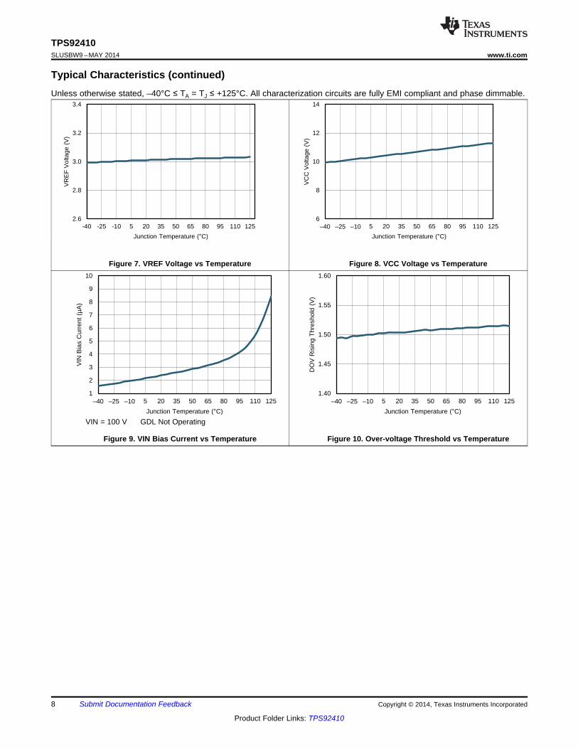
6.6 Typical CharacteristicsUnless otherwise stated, –40°C ≤ TA = TJ ≤ +125°C. All characterization circuits are fully EMI compliant and phase dimmable.
230 VAC 11.2 W Input Top stack = 160 V120VAC 6.8 W Input Top stack = 80 VMiddle stack = 80 V Bottom stack= 40 V VADIM = 1.5 VMiddle stack = 40 V Bottom stack= 20 V VADIM = 1.5 V
Figure 2. System Input Current vs Input VoltageFigure 1. System Input Current vs Input Voltage
230 VAC 11.2 W Input Top stack = 160 V120VAC 6.8 W Input Top stack = 80 VMiddle stack = 80 V Bottom stack= 40 VMiddle stack = 40 V Bottom stack= 20 V
Figure 4. System Input Current vs ADIM VoltageFigure 3. System Input Current vs ADIM Voltage
120VAC 6.8 W Input Top stack = 80 V 230 VAC 11. W Input Top stack = 160 VMiddle stack = 40 V Bottom stack= 20 V VADIM = 1.5 V Middle stack = 80 V Bottom stack= 40 V VADIM = 1.5 V
Figure 5. System Input Current vs TSNS Voltage Figure 6. System Input Current vs TSNS Voltage
Copyright © 2014, Texas Instruments Incorporated Submit Documentation Feedback 7
Product Folder Links: TPS92410
1
2
3
4
5
6
7
8
9
10
±40 ±25 ±10 5 20 35 50 65 80 95 110 125
VIN
Bia
s C
urre
nt (
µA
)
Junction Temperature (C) C015
1.40
1.45
1.50
1.55
1.60
±40 ±25 ±10 5 20 35 50 65 80 95 110 125
DO
V R
isin
g T
hres
hold
(V
)
Junction Temperature (C) C016
2.6
2.8
3.0
3.2
3.4
-40 -25 -10 5 20 35 50 65 80 95 110 125
VR
EF
Vol
tage
(V
)
Junction Temperature (C) C013
6
8
10
12
14
±40 ±25 ±10 5 20 35 50 65 80 95 110 125
VC
C V
olta
ge (
V)
Junction Temperature (C) C014
TPS92410SLUSBW9 –MAY 2014 www.ti.com
Typical Characteristics (continued)Unless otherwise stated, –40°C ≤ TA = TJ ≤ +125°C. All characterization circuits are fully EMI compliant and phase dimmable.
Figure 7. VREF Voltage vs Temperature Figure 8. VCC Voltage vs Temperature
VIN = 100 V GDL Not Operating
Figure 9. VIN Bias Current vs Temperature Figure 10. Over-voltage Threshold vs Temperature
8 Submit Documentation Feedback Copyright © 2014, Texas Instruments Incorporated
Product Folder Links: TPS92410

VIN
VCC
A0
A1
A2
SD
1.5 V
VREF
1.5 V
ADIM
TSNS
gM
MULT
+
SD
CS
GDL
GND
SD
MULT
CPS CDD COMP
DOV
40 mV/20 mV
Thermal Shutdown
HV Bias RegulatorThermal
Shutdown
UVLO
3-VReference
Min .(A0, A1, A2) .
SD
AMUXSel
OVP
Dimmer Detection
S Q
R
TimerEdgedv/dt
TPS92410www.ti.com SLUSBW9 –MAY 2014
7 Detailed Description
7.1 OverviewThe TPS92410 device is a high-voltage linear regulator driver that can be used for offline LED drivers. It includesa feature that forces the regulator current to follow the rectified AC voltage to achieve high power-factor and lowtotal harmonic distortion (THD). When the device detects multiple forward phase dimmer edges, the regulatorcurrent changes to a DC level to maintain a DC current draw to provide for a triac dimmer's hold currentrequirements. The TPS92410 device also includes linear MOSFET over-voltage protection to protect theMOSFET if the LEDs are shorted. It includes a thermal foldback feature to protect the entire circuit in the event itbecomes overheated. Analog dimming capability allows light output to be controlled by a microcontroller or a 0 Vto 10 V dimmer. The device also includes a precision voltage reference.
7.2 Functional Block Diagram
Copyright © 2014, Texas Instruments Incorporated Submit Documentation Feedback 9
Product Folder Links: TPS92410

RGND × CGND = 5 × dt
dt = CUPPER × VUPPER
IUPPER
VHYS-DOV = 20 µA × RDRAIN
RDRAIN = RGROUND × VOVP - 1.5 V
1.5 V
RCS =VIN(rms ) × 1.428
PIN
TPS92410SLUSBW9 –MAY 2014 www.ti.com
7.3 Feature Description
7.3.1 Setting the Linear Regulator Current/Input Power (CS)The input power (PIN) can be set with a resistor from the CS pin to ground. Calculate the value of the RCS resistorusing the following equation (see Figure 11):
where• VIN(rms) is the nominal rms input voltage to the circuit (1)
This sets the input power level due to the linear regulator for a standard application with VADIM and VTSNS greaterthan or equal to 1.5 V. If either pin is pulled below 1.5 V the input power scales accordingly to the ratio ofVTSNS/ADIM/1.5 V. The actual input power of the circuit is higher due to variables such as VIN bias current,resistor, diode, and other losses. When using forward phase dimmers there can be a significant current spikethrough the MOSFET and RCS depending on the dv/dt of the dimmer edge. The magnitude and duration of thiscurrent spike should be measured in any application and a resistor should be chosen that is rated for the peakcurrent required in any final design.
7.3.2 Over-Voltage Protecton (DOV)The DOV pin can be used to set an over-voltage protection threshold for the external linear MOSFET. Duringnormal operation DOV is not active, but in the event that the LEDs become shorted resulting in excessive voltageand power dissipation in the MOSFET over-voltage protection becomes active. During an over-voltage event, theCS pin regulation voltage defaults to 100 mV to reduce power dissipation in the MOSFET but still provide somelight with the remaining LEDs. For this reason it is recommended to use a nominal value for CS for normaloperation higher than 100 mV. A resistor divider to DOV between the MOSFET drain and system ground setsthis over-voltage level as shown in Figure 11. During an over-voltage event the DOV pin sources 1 µA to providesome hysteresis. The level and hysteresis can be set using the following equations:
(2)
where• VOVP is the desired maximum drain voltage• RDRAIN is the resistor from DOV to the drain• RGROUND is the resistor from DOV to system ground (3)
Include a capacitor from the DOV pin to system ground to prevent the circuit from transitioning into over-voltageprotection mode during the start-up sequence. A recommended value for the RGND resistor is 121 kΩ in parallelwith a 4.7-µF capacitor for most applications. RDRAIN can then be calculated. To calculate the values of RGNDand CGND for a particular application you need to set the time constant to be longer than it takes to charge upthe highest voltage LED string capacitor to prevent a false trip of the over-voltage protection during start-up. Thistime constant and the resulting RC can be found using the following equations:
(4)
where• dt is the time constant to charge the LED capacitor• CUPPER is the highest voltage LED string capacitor• VUPPER is the highest string voltage• IUPPER is the highest voltage LED string current (5)
Choose RGND to be in the 100 kΩ to 150 kΩ range and calculate CGND. Then RDRAIN can be calculated. Over-voltage protection should be adjusted for the minimum string voltages for analog dimming applications or simplydisabled by connecting DOV to ground.
10 Submit Documentation Feedback Copyright © 2014, Texas Instruments Incorporated
Product Folder Links: TPS92410

dtCDD = infinite (for dtCPS <TPER
11)
dtCPS = CCPS × 1.5 V
10 µA
RCS
DOV
RDRAIN
RGND
CGND
GDL
CS
VS
TPS92410www.ti.com SLUSBW9 –MAY 2014
Feature Description (continued)
Figure 11. CS and DOV Over-voltage Connections
7.3.3 Input Undervoltage Lockout (UVLO)The TPS92410 device includes input UVLO protection. This protection prevents the device from operating until avoltage on the VIN pin exceeds 8.0 V. The circuit has 2.15 V of hysteresis to prevent false triggering.
7.3.4 Reference Voltage (VREF)The TPS92410 includes a 3-V reference feature which can be used to set the DC level on the ADIM pin. It canalso source current for the TSNS divider for the thermal foldback circuitry using the TSNS pin. The VREF pin cansupply a maximum current of approximately 3 mA but should be limited to less than 200 μA to minimize powerdissipation. All current sourced from VREF is supplied by VIN so power dissipation can become significant whensourcing higher currents.
7.3.5 Forward Phase Dimmer Detection (CPS, CDD)An edge-detect circuit senses when a forward phase dimmer is connected to the input. This detection featureallows the device to operate with a wide variety of dimmers that operate in either forward or reverse phase. TheCCPS and CCDD capacitors assist in this function while preventing a false dimmer detect caused by line glitchesand spikes in applications without a phase dimmer. Connect a 0.1-μF capacitor between CPS to GND and a 1-μF capacitor from CDD to GND for most applications to use this feature. This results in a time constant of 15 msfor CPS and 150 ms for CDD. If this feature is not required leave CPS open and ground CDD.
The dimmer detect function operates by applying a 10 µA charging current to both the CPS and CDD capacitors.If no edges are detected the CPS capacitor charges to a 1.5 V threshold at which point the CDD pin switchesfrom sourcing 10 µA to sinking 1 µA. This prevents the CDD pin from charging to the 1.5-V threshold thatswitches the device to dimmer detect mode. When a forward phase dimmer is present the edge is detected atthe MULT pin. Each time an edge is detected the CPS pin is discharged and then begins charging again. Whenenough consecutive edges are present to keep the CPS pin below 1.5 V for longer than the CDD time constantthe CDD pin reaches 1.5 V and the device switches to dimmer detect mode. The current regulation levelbetween constant current dimmer detect mode and standard PFC operation can be different depending ondimmer angle. A time constant too long can result in a mild light difference at turn-on due to a slightly differentlight level between PFC mode at turn-on and dimmer detect mode. A time constant too short could result inunintentionally switching to dimmer detect mode on noisy lines. The easiest way to implement a dimmer detectcircuit is to use a CPS time constant just a bit longer than TPER, the period of half of the sine wave input voltage.But other time constants may be used if required. To change the time constants use the following equations:
(6)
(7)
Copyright © 2014, Texas Instruments Incorporated Submit Documentation Feedback 11
Product Folder Links: TPS92410

BW = gM
tN× CCOMP
dtCDD = CCDD × 1.5 V
10 µA (for dtCPS > TPER )
dtCDD = CCDD × 1.5 V
:11 µA × dtCPS ;F (1 µA × TPER ) (for
TPER
11< dtCPS < TPER )
TPS92410SLUSBW9 –MAY 2014 www.ti.com
Feature Description (continued)
(8)
(9)
7.3.6 Analog Dimming Input and Setting VCS (ADIM)If a default CS voltage of lower than 1.291 V is required, it can be set using the ADIM pin. A resistor divider fromthe reference sets ADIM to any voltage lower than 1.5 V. During normal operation, the CS voltage is equal to0.86 times the voltage applied to ADIM. The ADIM pin can also be used for analog dimming using a variablevoltage between 40 mV and 1.5 V to dynamically change the CS voltage. If the device pulls the ADIM pin below40 mV, the device pulls the linear MOSFET gate low to shut off the LEDs. Tie an unused ADIM pin to VREF witha 200-kΩ resistor. If a larger analog dimming range is required, use the TSNS pin for analog dimming because itdoes not disable the linear regulator when the voltage drops below 40 mV. The ADIM and TSNS pins functionidentically with the exception of the GDL disable threshold on the ADIM pin.
7.3.7 Thermal Foldback (TSNS)The thermal foldback function of the TPS92410 device behaves similarly to the ADIM function. However, ratherthan using a resistor divider, a NTC thermistor connects TSNS to system ground. Calculate the temperature atwhich the circuit begins to reduce current by determining the temperature at which the the TSNS pin drops below1.5 V (when the ADIM pin is 1.5 V or higher). With a valid external voltage on the ADIM pin (< 1.5 V), the currentbegins to reduce when the TSNS voltage drops lower than the ADIM voltage. As described in the AnalogDimming Input and Setting VCS (ADIM) section, the TSNS pin and the ADIM pin may be used interchangeably. Ifthe TSNS pin is used for analog dimming, the ADIM pin may be used for thermal foldback.
7.3.8 Internal Regulator (VCC)The VCC pin functions as the output of the internal supply for the device. Connect a 10-µF capacitor between theVCC pin and ground to keep VCC charged for phase dimming applications. For analog dimming or non-dimmingapplications a 4.7-µF capacitor is sufficient.
7.3.9 Error Amplifier (COMP)The COMP pin functions as the output of the internal gM error amplifier. To ensure stability over all conditions,connect a 4.7-µF capacitor between the COMP pin and ground. The bandwidth of the PFC can be calculatedusing the following equation:
(10)
7.3.10 Linear MOSFET Gate Drive (GDL)The GDL pin functions as the gate drive for the linear MOSFET that regulates current. Connect the GDL pin tothe gate of the power MOSFET. To reduce EMI, connect a 10-Ω resistor in series with a 1-µF capacitor betweenthe GDL pin and the CS pin with a diode connected between them that returns to the VCC pin as show inFigure 12. If phase dimming is not required, the diode can be omitted. Choose a linear MOSFET with a voltagerating of at least 250 V for a 120-VAC input application. Choose a linear MOSFET with a voltage rating of at least400 V for a 230-VAC input application. The MOSFET voltage rating must take into account the MOV clampvoltage in protected applications as this may be higher than the MOSFET and damage may occur during a surgeevent. The Safe Operating Area (SOA) of the MOSFET must also be taken into account. During start-up theMOSFET experiences high voltages as the LED capacitors charge. This leads to high power dissipation duringstart-up that the MOSFET must withstand. Use with forward phase dimmers also causes a significant currentspike in the MOSFET when the dimmer fires. The magnitude and duration of this current spike is dependentupon many factors and should be measured in any design to confirm the MOSFET is rated properly for long lifeoperation. MOSFET parasitics should also be considered. A very large MOSFET with high parasitic capacitancescan cause erroneous switching of the TPS92411 floating drivers.
12 Submit Documentation Feedback Copyright © 2014, Texas Instruments Incorporated
Product Folder Links: TPS92410
TPS92410www.ti.com SLUSBW9 –MAY 2014
Feature Description (continued)7.3.11 EMI FilterThe input EMI filter requirements are specific to each design. A capacitor is needed for filtering and may alsorequire an input resistor. For forward phase applications a snubber across the capacitor is likely to be required.The input resistor and snubber resistor need to have a pulse rating high enough for the particular applicationboth during start-up and during forward phase dimming.
7.3.12 Thermal ShutdownThe TPS92410 device includes thermal shutdown protection. If the die temperature reaches approximately175°C the device shuts down. When the die temperature cools to approximately 165°C, the device resumesnormal operation.
7.4 Device Functional Modes
7.4.1 Multiplier ModeWhen the MULT pin detects full rectified AC voltage, the CS voltage follows the rectified AC waveform around itsregulation point. This behavior forces the current that is drawn from the line to follow the AC input voltagewaveform. This action results in high power factor and low total harmonic distortion (THD). Line transients arerejected by the time constant that is initially set on the dimmer detect circuit to ensure dimmer detect mode is notengaged by random voltage spikes on the line.
7.4.2 Dimmer Detect ModeWhen a forward phase dimmer is present there is a sharp edge presented to the MULT pin each cycle. Thisforces the dimmer detect circuit past its time constant and the device enters dimming mode. The CS voltage isthen set at a DC level to prevent dimmer misfire
8 Application and Implementation
8.1 Application InformationThe TPS92410 is a linear controller designed to be used in conjunction with the TPS92411 switch for highvoltage off-line LED drive applications. Typical uses include 120 VAC and 230 VAC input LED drivers with eitheranalog or phase dimming. However like any linear controller it may also be used with a DC input voltage up to450 V. The following applications are for typical off-line LED drivers with 120 VAC and 230 VAC input voltages.
Copyright © 2014, Texas Instruments Incorporated Submit Documentation Feedback 13
Product Folder Links: TPS92410
VIN
RSET
TPS92411
RSNS
DRAIN
VS33 µF100 V
VIN
RSET
TPS92411
RSNS
DRAIN
VS
VIN
RSET
TPS92411
RSNS
DRAIN
VS
± +
120 VRMS
22
0.15 µF(1)
250 V
442 (1)
0.047 µF250 V
1.82 0
1.65 0
1.43 0
1 0
1 0
1 0
200 V
200 V
68 µF50 V
200 V
120 µF25 V
VIN
MULT
VREF
ADIM
TSNS
2 0
30.1 N
0.1 PF
30.1 N
470 NNTC VCC COMP GND
CDD
DOV
CS
CPS0.1 PF(1)
1 PF(1)
GDL
121 N 4.7 PF
2 0
10
1 PF
VCC(1)
55 N(1)
4.7 PF10 PF25 V
RCS30.1
TPS92410
128
TPS92410SLUSBW9 –MAY 2014 www.ti.com
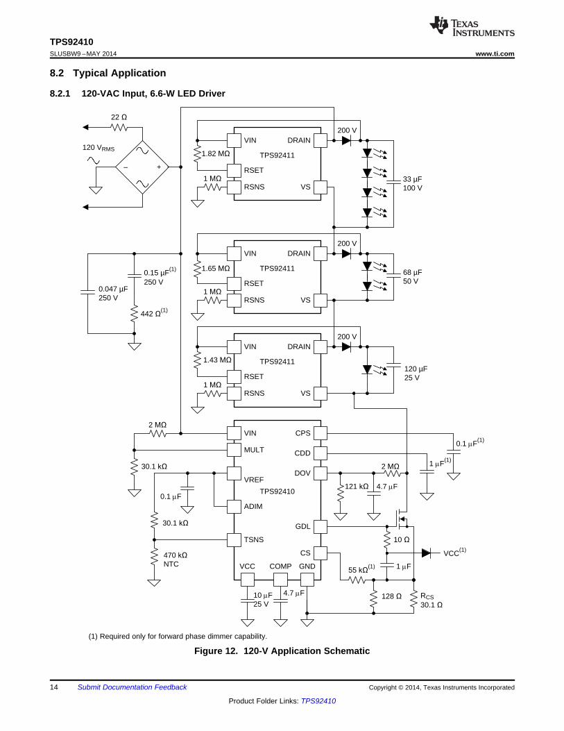
8.2 Typical Application
8.2.1 120-VAC Input, 6.6-W LED Driver
(1) Required only for forward phase dimmer capability.
Figure 12. 120-V Application Schematic
14 Submit Documentation Feedback Copyright © 2014, Texas Instruments Incorporated
Product Folder Links: TPS92410

0.95
0.96
0.97
0.98
0.99
1.00
85 95 105 115 125 135
Pow
er F
acto
r
Input Voltage (VAC) C002
0
2
4
6
8
10
85 95 105 115 125 135
TH
D (
%)
Input Voltage (VAC) C003
TPS92410www.ti.com SLUSBW9 –MAY 2014
Typical Application (continued)8.2.1.1 Design RequirementsThis application requires a 6.6-W input power, high-efficiency, phase-dimmable LED lamp for use on 120-Vsystems.
8.2.1.2 Detailed Design ProcedureThe TPS92411 components are chosen using the guidelines in the TPS92411 datasheet. Most of the valuesused for the TPS92410 are recommended values for any 120-V system. Connect the input voltage directly to therectified AC while the MULT pin is connected to a 2-MΩ, 30.1-kΩ resistor divider from the rectified AC to ground.The VREF pin should have a 0.1-µF capacitor tied to ground for decoupling. The VCC pin should be decoupledusing a 10-µF ceramic capacitor to ground and the COMP pin should have a 4.7-µF ceramic capacitor to ground.Connect a 0.1-µF ceramic capacitor from the CPS pin to ground. Connect a 1-µF ceramic capacitor from theCDD pin to ground to enable phase dimmable operation. This results in a 150 ms dimmer detect time constant.The over-voltage protection using the DOV pin can be set using Equation 3. In this case a MOSFET drain over-voltage level of approximately 27 V is chosen. A 4.7-µF capacitor should be placed in parallel with a 121-kΩresistor from the DOV pin to ground to set a time constant and for filtering for all applications.
Choose RDRAIN for the appropriate voltage, in this case 2 MΩ is chosen. Connect a 10-Ω resistor in series with a1-µF ceramic capacitor from GDL to CS for stability and to help reduce EMI. Place a diode from the center pointof these two components to the VCC pin to clamp the voltage on the GDL pin and the CS pin that can becomehigh with some forward phase dimmers. A rating of at least 20 V and 100 mA is recommended with a peak-repetitive current rating of at least 2 A. A 55-kΩ resistor should be connected between the MOSFET source andthe CS pin for additional protection. Connect a 30.1-kΩ resistor from the TSNS pin to the VREF pin. The NTCthermistor to ground should be selected so that the desired foldback temperature results in a thermistor value of30.1 kΩ. RCS is then calculated using Equation 1. RCS = 25 Ω is very close, a 30.1 Ω in parallel with a 182 Ωresulting in about 25.83 Ω was chosen.
8.2.1.3 Application Curves
120VAC Top stack = 80 V 6.8 W Input 120VAC Top stack = 80 V 6.8 W InputMiddle stack = 40 V Bottom stack= 20 V VADIM = 1.5 V Middle stack = 40 V Bottom stack= 20 V VADIM = 1.5 V
Figure 13. Power Factor vs Input Voltage Figure 14. Total Harmonic Distortion vs Input Voltage
Copyright © 2014, Texas Instruments Incorporated Submit Documentation Feedback 15
Product Folder Links: TPS92410

VIN
RSET
TPS92411
RSNS
DRAIN
VS
0.1 µF100 V
VIN
RSET
TPS92411
RSNS
DRAIN
VS
VIN
RSET
TPS92411
RSNS
DRAIN
VS
± +
230 VRMS
68
0.15 µF(1)
400 V
410 (1)
0.033 µF400 V
1.91 0
1.82 0
1.69 0
1 0
1 0
1 0
200 V
200 V
47 µF100 V
200 V
100 µF50 V
12 V 12 V
22 µF200 V
1 0
10 N
680 pF1 N Q3200 VVGS = 4 V
VIN
MULT
VREF
ADIM
TSNS
4 0
30.1 N
0.1 PF
30.1 N
470 NNTC VCC COMP GND
CDD
DOV
CS
CPS0.1 PF(1)
1 PF(1)
GDL
121 N 4.7 PF
4 0
10
1 PF
VCC(1)
55 N(1)
4.7 PF10 PF25 V
RCS30.1
TPS92410SLUSBW9 –MAY 2014 www.ti.com
Typical Application (continued)8.2.2 230-VAC Input, 11-W LED Driver
(1) Required only for forward phase dimmer capability.
Figure 15. 230-V Application Schematic
16 Submit Documentation Feedback Copyright © 2014, Texas Instruments Incorporated
Product Folder Links: TPS92410

0.95
0.96
0.97
0.98
0.99
1.00
190 200 210 220 230 240 250 260
Pow
er F
acto
r
Input Voltage (VAC) C007
0
3
6
9
12
15
190 200 210 220 230 240 250 260
TH
D (
%)
Input Voltage (VAC) C008
TPS92410www.ti.com SLUSBW9 –MAY 2014
Typical Application (continued)8.2.2.1 Design RequirementsThis application requires a 11-W input power, high-efficiency, phase-dimmable LED lamp for use on 230-Vsystems.
8.2.2.2 Detailed Design ProcedureThe TPS92411 components are chosen using the guidelines in the TPS92411 datasheet. Most of the valuesused for the TPS92410 are recommended values for any 230-V system. The input voltage should be connecteddirectly to rectified AC while the MULT pin is connected to a 4-MΩ, 30.1-kΩ resistor divider between rectified ACand ground. The VREF pin should have a 0.1-µF capacitor connected to ground to provide decoupling. The VCCpin should be decoupled using a 10-µF ceramic capacitor to ground and the COMP pin should have a 4.7-µFceramic capacitor to ground. Connect a 0.1-µF ceramic capacitor from the CPS pin to ground. Connect a 1-µFceramic capacitor from CDD to ground to enable phase dimmable operation. This results in a 150 ms dimmerdetect time constant. The over-voltage protection using the DOV pin can be set using Equation 3. This caseincludes a MOSFET drain over-voltage level of approximately 51 V. A 4.7-µF capacitor should be placed inparallel with a 121-kΩ resistor from the DOV pin to ground to set a time constant and for filtering for allapplications.
Choose RDRAIN for the appropriate voltage, this case uses a value of 4-MΩ. A 10-Ω resistor in series with a 1-µFceramic capacitor from GDL to CS adds stability and helps reduce EMI. A diode should be placed from thecenter point of these two components to the VCC pin to clamp the voltage on the GDL pin and the CS pin thatcan become high with some forward phase dimmers. A rating of at least 20 V and 100 mA is recommended witha peak-repetitive current rating of at least 2 A. A 55-kΩ resistor should be connected between the MOSFETsource and the CS pin for additional protection. Connect a 30.1-kΩ resistor from the TSNS pin to the VREF pin.The NTC thermistor to ground should be selected so that the desired foldback temperature results in a thermistorvalue of 30.1 kΩ. RCS is then calculated using Equation 1. RCS = 30.1 Ω is very close and was chosen for thisdesign.
8.2.2.3 Application Curves
Top stack = 160 V 11.2 W Input 230 VAC Top stack = 160 V 11.2 W Input 230 VACMiddle stack = 80 V Bottom stack= 40 V VADIM = 1.5 V Middle stack = 80 V Bottom stack= 40 V VADIM = 1.5 V
Figure 16. Power Factor vs Input Voltage Figure 17. Total Harmonic Distortion vs Input Voltage
Copyright © 2014, Texas Instruments Incorporated Submit Documentation Feedback 17
Product Folder Links: TPS92410

To VCC
CPS
CDD
DOV
GDL
VIN
GND
COMP
VREF
VCC
MULT
TSNS
ADIM
CS
To source of bottom
TPS92411
To rectified AC1
2
3
7
5
6
4
14
12
11
10
9
8
TPS92410SLUSBW9 –MAY 2014 www.ti.com
9 Power Supply RecommendationsFor testing purposes any benchtop adjustable AC power supply with a power rating higher than what is requiredby the circuit is suitable. An example would be an Hewlett Packard 6811B or equivalent. An isolated supply isrecommended for safety purposes.
10 LayoutProper layout is important in any regulator design. The TPS92410 is a linear regulator which simplifies layoutcompared to a switching regulator, however some consideration should be taken.
10.1 Layout GuidelinesComponents between CPS, CDD, DOV, COMP, VREF, MULT, and VCC to ground (GND) should be placeddirectly next to the device as shown in Figure 18. The linear MOSFET as well as the GDL and CS traces shouldbe placed as close the TPS92410 as possible as well.
10.2 Layout Example
Figure 18. Recommended Component Placement
18 Submit Documentation Feedback Copyright © 2014, Texas Instruments Incorporated
Product Folder Links: TPS92410

TPS92410www.ti.com SLUSBW9 –MAY 2014
11 Device and Documentation Support
11.1 Trademarks
11.2 Electrostatic Discharge CautionThese devices have limited built-in ESD protection. The leads should be shorted together or the device placed in conductive foamduring storage or handling to prevent electrostatic damage to the MOS gates.
11.3 GlossarySLYZ022 — TI Glossary.
This glossary lists and explains terms, acronyms, and definitions.
Copyright © 2014, Texas Instruments Incorporated Submit Documentation Feedback 19
Product Folder Links: TPS92410

TPS92410SLUSBW9 –MAY 2014 www.ti.com
12 Mechanical, Packaging, and Orderable InformationThe following pages include mechanical, packaging, and orderable information. This information is the mostcurrent data available for the designated devices. This data is subject to change without notice and revision ofthis document. For browser-based versions of this data sheet, refer to the left-hand navigation.
20 Submit Documentation Feedback Copyright © 2014, Texas Instruments Incorporated
Product Folder Links: TPS92410

PACKAGE OPTION ADDENDUM
www.ti.com 6-Aug-2016
Addendum-Page 1
PACKAGING INFORMATION
Orderable Device Status(1)
Package Type PackageDrawing
Pins PackageQty
Eco Plan(2)
Lead/Ball Finish(6)
MSL Peak Temp(3)
Op Temp (°C) Device Marking(4/5)
Samples
TPS92410D ACTIVE SOIC D 13 50 Green (RoHS& no Sb/Br)
CU NIPDAU Level-2-260C-1 YEAR -40 to 150 TPS92410D
TPS92410DR ACTIVE SOIC D 13 2500 Green (RoHS& no Sb/Br)
CU NIPDAU Level-2-260C-1 YEAR -40 to 150 TPS92410D
(1) The marketing status values are defined as follows:ACTIVE: Product device recommended for new designs.LIFEBUY: TI has announced that the device will be discontinued, and a lifetime-buy period is in effect.NRND: Not recommended for new designs. Device is in production to support existing customers, but TI does not recommend using this part in a new design.PREVIEW: Device has been announced but is not in production. Samples may or may not be available.OBSOLETE: TI has discontinued the production of the device.
(2) Eco Plan - The planned eco-friendly classification: Pb-Free (RoHS), Pb-Free (RoHS Exempt), or Green (RoHS & no Sb/Br) - please check http://www.ti.com/productcontent for the latest availabilityinformation and additional product content details.TBD: The Pb-Free/Green conversion plan has not been defined.Pb-Free (RoHS): TI's terms "Lead-Free" or "Pb-Free" mean semiconductor products that are compatible with the current RoHS requirements for all 6 substances, including the requirement thatlead not exceed 0.1% by weight in homogeneous materials. Where designed to be soldered at high temperatures, TI Pb-Free products are suitable for use in specified lead-free processes.Pb-Free (RoHS Exempt): This component has a RoHS exemption for either 1) lead-based flip-chip solder bumps used between the die and package, or 2) lead-based die adhesive used betweenthe die and leadframe. The component is otherwise considered Pb-Free (RoHS compatible) as defined above.Green (RoHS & no Sb/Br): TI defines "Green" to mean Pb-Free (RoHS compatible), and free of Bromine (Br) and Antimony (Sb) based flame retardants (Br or Sb do not exceed 0.1% by weightin homogeneous material)
(3) MSL, Peak Temp. - The Moisture Sensitivity Level rating according to the JEDEC industry standard classifications, and peak solder temperature.
(4) There may be additional marking, which relates to the logo, the lot trace code information, or the environmental category on the device.
(5) Multiple Device Markings will be inside parentheses. Only one Device Marking contained in parentheses and separated by a "~" will appear on a device. If a line is indented then it is a continuationof the previous line and the two combined represent the entire Device Marking for that device.
(6) Lead/Ball Finish - Orderable Devices may have multiple material finish options. Finish options are separated by a vertical ruled line. Lead/Ball Finish values may wrap to two lines if the finishvalue exceeds the maximum column width.
Important Information and Disclaimer:The information provided on this page represents TI's knowledge and belief as of the date that it is provided. TI bases its knowledge and belief on informationprovided by third parties, and makes no representation or warranty as to the accuracy of such information. Efforts are underway to better integrate information from third parties. TI has taken andcontinues to take reasonable steps to provide representative and accurate information but may not have conducted destructive testing or chemical analysis on incoming materials and chemicals.TI and TI suppliers consider certain information to be proprietary, and thus CAS numbers and other limited information may not be available for release.

PACKAGE OPTION ADDENDUM
www.ti.com 6-Aug-2016
Addendum-Page 2
In no event shall TI's liability arising out of such information exceed the total purchase price of the TI part(s) at issue in this document sold by TI to Customer on an annual basis.
TAPE AND REEL INFORMATION
*All dimensions are nominal
Device PackageType
PackageDrawing
Pins SPQ ReelDiameter
(mm)
ReelWidth
W1 (mm)
A0(mm)
B0(mm)
K0(mm)
P1(mm)
W(mm)
Pin1Quadrant
TPS92410DR SOIC D 13 2500 330.0 16.4 6.5 9.0 2.1 8.0 16.0 Q1
PACKAGE MATERIALS INFORMATION
www.ti.com 21-Oct-2014
Pack Materials-Page 1

*All dimensions are nominal
Device Package Type Package Drawing Pins SPQ Length (mm) Width (mm) Height (mm)
TPS92410DR SOIC D 13 2500 367.0 367.0 38.0
PACKAGE MATERIALS INFORMATION
www.ti.com 21-Oct-2014
Pack Materials-Page 2
IMPORTANT NOTICE
Texas Instruments Incorporated and its subsidiaries (TI) reserve the right to make corrections, enhancements, improvements and otherchanges to its semiconductor products and services per JESD46, latest issue, and to discontinue any product or service per JESD48, latestissue. Buyers should obtain the latest relevant information before placing orders and should verify that such information is current andcomplete. All semiconductor products (also referred to herein as “components”) are sold subject to TI’s terms and conditions of salesupplied at the time of order acknowledgment.TI warrants performance of its components to the specifications applicable at the time of sale, in accordance with the warranty in TI’s termsand conditions of sale of semiconductor products. Testing and other quality control techniques are used to the extent TI deems necessaryto support this warranty. Except where mandated by applicable law, testing of all parameters of each component is not necessarilyperformed.TI assumes no liability for applications assistance or the design of Buyers’ products. Buyers are responsible for their products andapplications using TI components. To minimize the risks associated with Buyers’ products and applications, Buyers should provideadequate design and operating safeguards.TI does not warrant or represent that any license, either express or implied, is granted under any patent right, copyright, mask work right, orother intellectual property right relating to any combination, machine, or process in which TI components or services are used. Informationpublished by TI regarding third-party products or services does not constitute a license to use such products or services or a warranty orendorsement thereof. Use of such information may require a license from a third party under the patents or other intellectual property of thethird party, or a license from TI under the patents or other intellectual property of TI.Reproduction of significant portions of TI information in TI data books or data sheets is permissible only if reproduction is without alterationand is accompanied by all associated warranties, conditions, limitations, and notices. TI is not responsible or liable for such altereddocumentation. Information of third parties may be subject to additional restrictions.Resale of TI components or services with statements different from or beyond the parameters stated by TI for that component or servicevoids all express and any implied warranties for the associated TI component or service and is an unfair and deceptive business practice.TI is not responsible or liable for any such statements.Buyer acknowledges and agrees that it is solely responsible for compliance with all legal, regulatory and safety-related requirementsconcerning its products, and any use of TI components in its applications, notwithstanding any applications-related information or supportthat may be provided by TI. Buyer represents and agrees that it has all the necessary expertise to create and implement safeguards whichanticipate dangerous consequences of failures, monitor failures and their consequences, lessen the likelihood of failures that might causeharm and take appropriate remedial actions. Buyer will fully indemnify TI and its representatives against any damages arising out of the useof any TI components in safety-critical applications.In some cases, TI components may be promoted specifically to facilitate safety-related applications. With such components, TI’s goal is tohelp enable customers to design and create their own end-product solutions that meet applicable functional safety standards andrequirements. Nonetheless, such components are subject to these terms.No TI components are authorized for use in FDA Class III (or similar life-critical medical equipment) unless authorized officers of the partieshave executed a special agreement specifically governing such use.Only those TI components which TI has specifically designated as military grade or “enhanced plastic” are designed and intended for use inmilitary/aerospace applications or environments. Buyer acknowledges and agrees that any military or aerospace use of TI componentswhich have not been so designated is solely at the Buyer's risk, and that Buyer is solely responsible for compliance with all legal andregulatory requirements in connection with such use.TI has specifically designated certain components as meeting ISO/TS16949 requirements, mainly for automotive use. In any case of use ofnon-designated products, TI will not be responsible for any failure to meet ISO/TS16949.
Products ApplicationsAudio www.ti.com/audio Automotive and Transportation www.ti.com/automotiveAmplifiers amplifier.ti.com Communications and Telecom www.ti.com/communicationsData Converters dataconverter.ti.com Computers and Peripherals www.ti.com/computersDLP® Products www.dlp.com Consumer Electronics www.ti.com/consumer-appsDSP dsp.ti.com Energy and Lighting www.ti.com/energyClocks and Timers www.ti.com/clocks Industrial www.ti.com/industrialInterface interface.ti.com Medical www.ti.com/medicalLogic logic.ti.com Security www.ti.com/securityPower Mgmt power.ti.com Space, Avionics and Defense www.ti.com/space-avionics-defenseMicrocontrollers microcontroller.ti.com Video and Imaging www.ti.com/videoRFID www.ti-rfid.comOMAP Applications Processors www.ti.com/omap TI E2E Community e2e.ti.comWireless Connectivity www.ti.com/wirelessconnectivity
Mailing Address: Texas Instruments, Post Office Box 655303, Dallas, Texas 75265Copyright © 2016, Texas Instruments Incorporated