Embed Size (px)
Citation preview

Survey on Photonics and Novel Op6cal Materials
Minghao Qi Purdue University
DLA 2011
SLAC Na=onal Accelerator Laboratory
September 15, 2011

Photonics and Novel Op=cal Materials
• Outline – On-‐chip hollow TM structures – On-‐chip accelerator based on Omniguide waveguides
– Fiber to waveguide couplers, power spliJers – Materials and Damage
– New fabrica=on approach to Woodpile 3D photonic crystals

On-‐Chip TM-‐Mode Waveguides • Must be hollow • Need to have a phase speed matched with the speed of the bunch – At high par=cle energy, phase velocity must match c
• Prefer to be strongly confined – Higher gradient
• Omniguide fiber, PhC fibers, 3D photonic crystals – Tunable to tolerate fabrica=on varia=ons – Low nonlinearity?

Omni-‐Guide Fibers
• Direct analogy with hollow metallic waveguides – Cylindrical symmetry may facilitate TM modes
• Also called Bragg Fibers
• We need to bring them onto chips
S. G. Johnson, et al, Op=cs Express, 9, 748-‐779, (2001)

Engineering Op=ons
• Indices: Red: 2.8, blue: 1.5 • TM band gap intersects light line.
T. D. Engeness, et al, Op=cs Express, 10, 1175-‐1196, (2003)

Hybrid Modes can Intersect Light Line
T. D. Engeness, et al, Op=cs Express, 10, 1175-‐1196, (2003)

Higher Order TM Modes Could Intersect with Light Line
G. Ouyang, et al, Op=cs Express, 10, 899-‐908, (2002)

Proposal of an On-‐Chip Accelerator
Electron bunches
Beam posi=on sensor
Accelera=on module
Focusing module
Laser input fiber, l1
Laser input fiber, l2
Si
W SiO2
• Inner diameters can be different and controlled

How to Fabricate It?
• Standard CMOS process except wafer bonding • Does not require deep submicron technology
• Can control the inner diameter
Si W
Si W
SiN SiN

Oxida=on to Achieve Circular Shape
• Require aligned wafer bonding (but just once) • Tungsten as quadruple-‐poles to withstand high temperature.
SiN SiN SiN SiN
Si
W
Si
W

Chop the hollow waveguide to right length
• Right module length for accelera=on and focusing • Short enough for atomic layer deposi=on to work

ALD to coat the inner Bragg layers
• Atomic Layer Deposi=on is extremely uniform
Short distance to waveguide terminals

Previous Demonstra=on on Chip
T. C. Shen, et al, Journal of Lightwave Technology, 28, 1714, (2011)
G. R. Hadley, et al, Op=cs LeJers, 29, 809, (2004)
• Not using ALD • With deposi=on of Si followed by oxida=on of Si

Other Approaches
Polymer protecting sidewall in Bosch process used as mask for isotropic etch with xenon difluoride Image courtesy of Carnegie Mellon University MEMs Laboratory
D. Gaugel, K. Gabriel, "CMOS-Compatible Micro-Fluidic Chip Cooling Using Buried Channel Fabrication," Proceedings of IMECE '02, New Orleans, 2002

Exposing the Quadruple Poles for beam sensing
• Or not necessary, if we only need to measure the posi=ons?
• Unlikely to be able to focus or deflect beam bunches?

Fiber Pigtailing
• The hollow coupler could be short and tapered • Fiber =ps could be tapered • Add heater to achieve tunability
TE mode
Short coupler
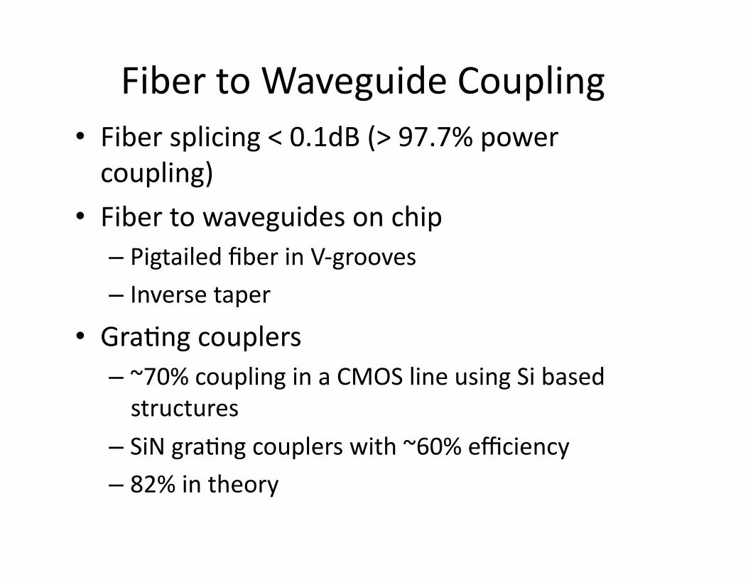
Fiber to Waveguide Coupling • Fiber splicing < 0.1dB (> 97.7% power coupling)
• Fiber to waveguides on chip – Pigtailed fiber in V-‐grooves – Inverse taper
• Gra=ng couplers – ~70% coupling in a CMOS line using Si based structures
– SiN gra=ng couplers with ~60% efficiency – 82% in theory

Inverse Taper for Fiber to Waveguide Coupling
• ~ 1dB loss per facet is predicted • ~1.6dB per facet loss realized
overcladding Silicon or SiN core
Silicon waveguides
Polymer waveguides Doped Silicon dioxide core
Undercladding

Gra=ng Coupler: Ver=cal to Horizontal coupling
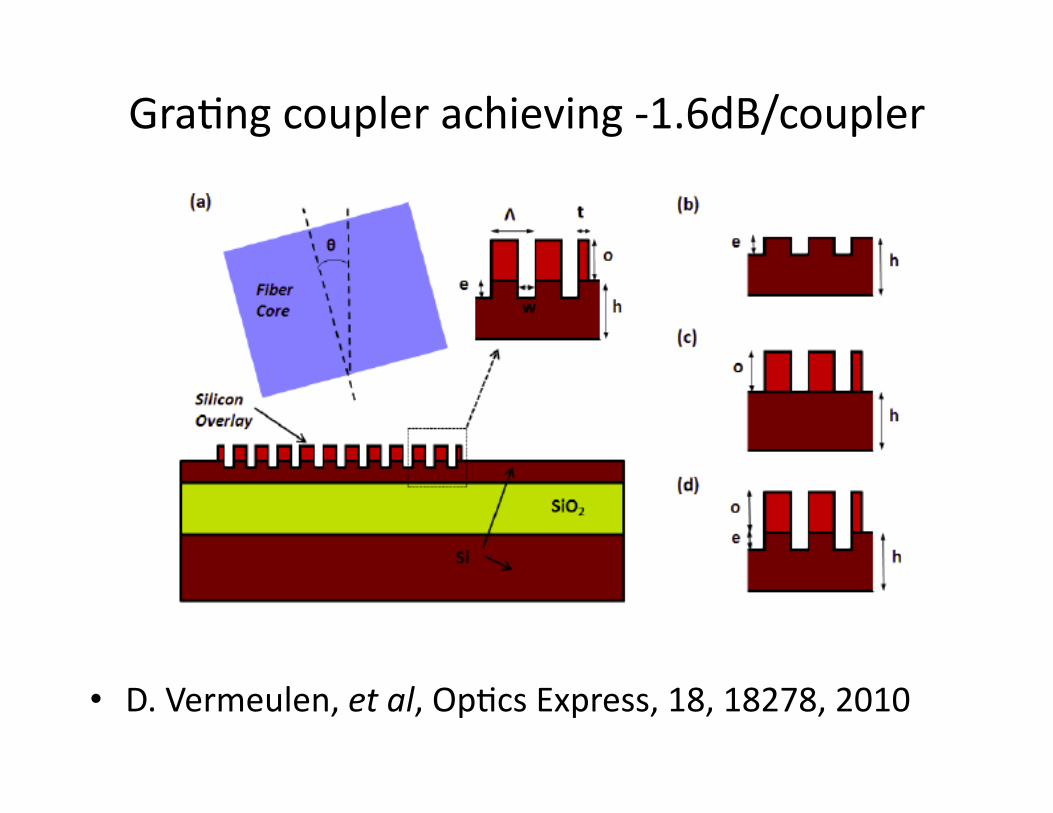
Gra=ng coupler achieving -‐1.6dB/coupler
• D. Vermeulen, et al, Op=cs Express, 18, 18278, 2010

220nm
150nm 220nm
370nm
240nm
Design op=miza=on
Ziran’s Design

Fabricated Si Gra=ng Coupler

Tes=ng setup: fiber bundle

Material Guidelines • High power handling capability
– High-‐damage threshold
– Low nonlinearity • Conduc=vity: avoid electron trapping
– Dielectrics – Semiconductor
– Metal – Graphene?
• CMOS compa=bility – SiO2, SiN, Si
• Other semiconductors or exo=c materials?

Material Damage • Con=nuous wave laser characteriza=on of gra=ng couplers – Can extract power enhancement factor from resonant structures.
• Si has high two-‐photon absorp=on probability – Generates free carriers – Absorbs light – Heat up structures
• Silicon nitride has larger band gap and does not suffer from two-‐photon absorp=on – Expected to have much higher damage threshold
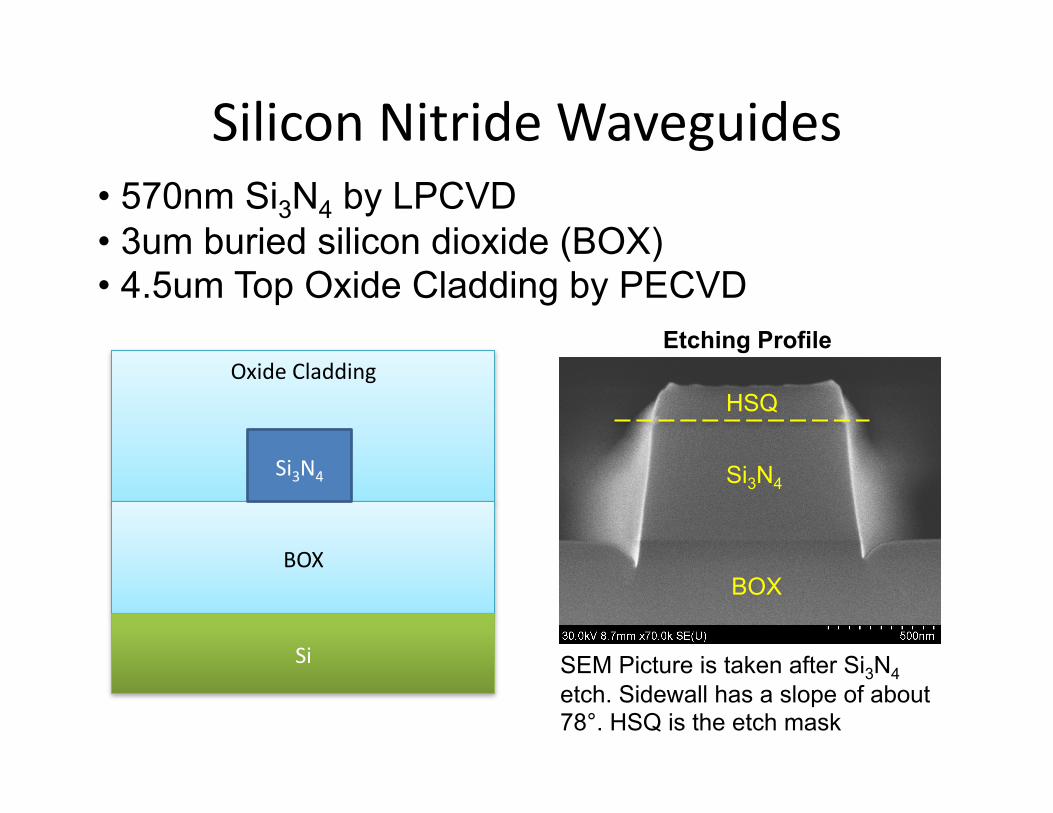
Silicon Nitride Waveguides • 570nm Si3N4 by LPCVD • 3um buried silicon dioxide (BOX) • 4.5um Top Oxide Cladding by PECVD
SEM Picture is taken after Si3N4 etch. Sidewall has a slope of about 78°. HSQ is the etch mask
Oxide Cladding
BOX
Si3N4
Si
Si3N4
HSQ
BOX
Etching Profile

Nitride Ring R=40um with Taper
• WG width = 1um
• Gap = 700nm
• 3dB bandwidth at 1558nm is about 7pm. • Q ≈ 223K low propagation loss ~ 2dB/cm • Grating couplers with SiN is being fabricated
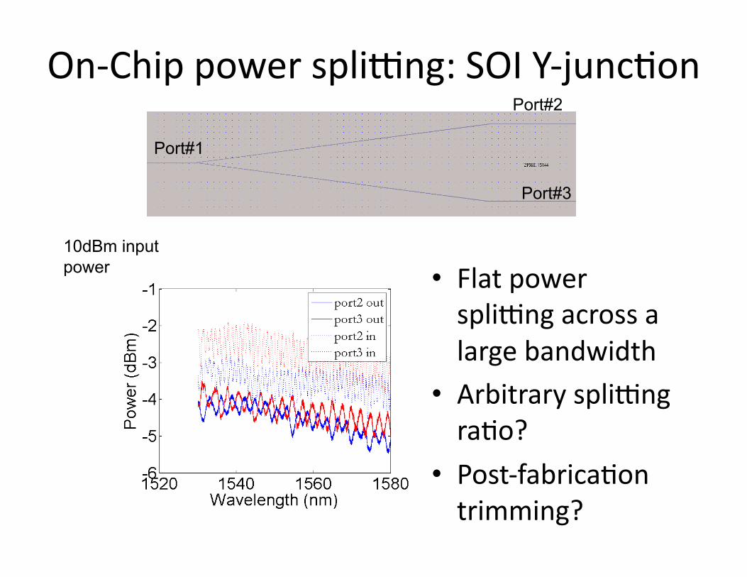
On-‐Chip power splipng: SOI Y-‐junc=on
• Flat power splipng across a large bandwidth
• Arbitrary splipng ra=o?
• Post-‐fabrica=on trimming?
Port#1
Port#2
Port#3
10dBm input power

Woodpile 3D Photonic Crystals • Best flexibility in
designing hollow waveguides
• 17 layers are needed
Layer 7
300 nm Si substrate
HSQ
6
1 2 3 4
5
100 nm
100 nm 300 nm

Membrane Transfer Technique 1. Fabricate all 17 layers in one step
+
+
+
2. Assemble layers to form 3D photonic crystal
waveguide

Woodpile structures before release
• Grating lines may stick together due to capillary forces – May need more spacers

Structures Released Successfully and Can be Stacked up
• The residuals are water debris and can be eliminated. • 2nd layer does not have the same debris.

Two layer Woodpile Structures with Reasonable Alignment
• Small particles within the membrane region. Can be avoided, we think.
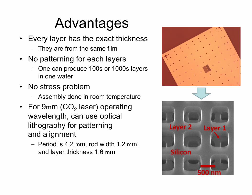
Advantages • Every layer has the exact thickness
– They are from the same film
• No patterning for each layers – One can produce 100s or 1000s layers
in one wafer
• No stress problem – Assembly done in room temperature
• For 9mm (CO2 laser) operating wavelength, can use optical lithography for patterning and alignment – Period is 4.2 mm, rod width 1.2 mm,
and layer thickness 1.6 mm
500 nm Silicon
Layer 1 Layer 2

3 Layer Membrane Bonding
• High precision alignment is required
1 2 Layer 3 Layer 1
Layer 2 Layer 3
Questions?