Embed Size (px)
Citation preview
Surface studies of phase formation in Co–Ge system:Reactive deposition epitaxy versus solid-phase epitaxy
I. Goldfarba)
Department of Solid Mechanics, Materials and Systems, The Fleischman Faculty of Engineering,Tel Aviv University, Ramat Aviv 69978, Israel
G.A.D. BriggsDepartment of Materials, University of Oxford, Parks Road, Oxford OX1 3PH, United Kingdom
(Received 25 May 2000; accepted 20 December 2000)
Morphological evolution of cobalt germanide epilayers, CoxGey, was investigatedin situ by scanning tunneling microscopy and spectroscopy and reflection high-energyelectron diffraction, as a function of deposition method and, hence, the phase contentof the epilayer. During reactive deposition epitaxy, in which Co atoms were evaporatedonto a flat pseudomorphic Ge/Si(001) wetting layer at 773 K, the first phase formedwas cobalt digermanide, CoGe2, in the form of elongated pyramidal islands. Each ofthese three-dimensional islands has locally exerted an additional strain on the Gewetting layer already strained at the Ge/Si(001) interface, lifting the layer metastabilityand causing, in turn, the formation of three-dimensional Ge pyramids underneath everyCoGe2 island. Solid-phase epitaxy of Co onto the same Ge/Si(001) epilayer resulted inthe formation of more Co-rich germanide islands. Coupling of strain from thesegermanides to the epitaxial Ge/Si(001) strain has also facilitated atwo-dimensional-to-three-dimensional transition of the Ge layer, however, with thegermanide islands located at the Ge pyramid troughs, rather than crests. The differencein the relative location of germanide and germanium islands in these two cases isexplained by accommodation of the large lattice-constant germanides at the morerelaxed regions of the Ge pyramid crests and the smaller lattice-constant at thecompressed Ge pyramid troughs.
I. INTRODUCTION
The interest in cobalt germanides, in particular CoGe2,stems from the fact that they can be used as a contactmaterial for Si1−xGex alloys and GaAs, and as infrareddetectors.1–5 Although there is a considerable amountof literature on crystallography, microstructure, phaseformation, and electronic properties of various cobaltsilicides due to their potential as self-aligned silicides,there are relatively few publications concerning struc-ture and properties of cobalt germanides. The data areincomplete and controversial. This is partly due to thecomplexity of the Co–Ge system and the different meth-ods of germanide synthesis used by various groups.1–7 Inaddition, because of the importance of contacts toSi1−xGex alloys, some groups investigate the reaction ofCo with Si1−xGex, rather than Ge, layers, which addscomplexity to the understanding of germanide formationkinetics.8–14 The equilibrium bulk-phase diagram con-
tains seven phases15: cubic Co3Ge, hexagonal Co5Ge2
(a 4 3.93 Å, c 4 5.01 Å), hexagonalb–Co5Ge3 andorthorhombica–Co5Ge3, monoclinic (a 4 11.65 Å,b 4 3.81 Å,c 4 4.95 Å) and cubic (a 4 4.64 Å) CoGe,tetragonal Co5Ge7 (a 4 7.64 Å,c 4 5.81 Å), orthorhom-bic CoGe2 (a 4 b 4 5.68 Å,c 4 10.82 Å), and Pearson’sCrystallographic Data contain also orthorhombic Co2Ge(a 4 5.02 Å, b 4 3.82 Å, c 4 7.26 Å).16 Co2Ge wasfound to form between Co and Ge layers after ion beammixing by Dhar and Kulkarni.4 Solid-phase epitaxy (SPE)of Co onto Ge/SiO2 followed by a 673–723 K anneal re-sulted in the formation of CoGe, which was transformedinto CoGe2 on an additional 923–1023 K anneal.5 Ashburnet al.1 found Co5Ge7 and CoGe2 in SPE of Co/Ge/Si(001)after a rapid thermal anneal (RTA) at 573 K and 698 K,respectively. Epitaxial CoGe2/GaAs was obtained by simul-taneous evaporation of Co and Ge+ using partially ionizedbeam deposition at 1:2 flux ratio.2,3 In addition to Co5Ge7
and CoGe2, Co3Ge2 was observed to form in metal vaporvacuum arc cobalt implanted germanium.6 Hence,a– andb–Co5Ge3 seem to appear only in the bulk form, whereasCo3Ge2 appears only during implantation. Diffusion
a)Address all correspondence to this author.e-mail: [email protected]
J. Mater. Res., Vol. 16, No. 3, Mar 2001 © 2001 Materials Research Society744
of Co through the Ge layer, with subsequent formation ofCoSi2 at the Ge/Si interface, i.e., Ge/CoSi2/Si, has beenwitnessed, as well.7
Not only the phase type but also the phase morphologydetermine the metal-semiconductor compound layerproperties. For example, although cobalt disilicide (CoSi2)exhibits exceptional properties as a self-aligned silicide,the use of epitaxial CoSi2 layers grown on Si(001) isimpeded by misoriented three-dimensional (3D) crystal-lites.17 To overcome this problem, the growth shouldtake place on a vicinal Si(001) surface,18 or a special“template” technique19–23should be used.
These two aspects, i.e., phase type and morphology,are not unrelated. Because each phase has its uniquelattice constant, resulting from its crystalline structureand bonding, this affects the lattice mismatch with theunderlying substrate. The elastic strain from this mis-match, combined with the relative surface and interfaceenergies, may, in turn, influence the surface morphologyof the growing layer.24 We show that different morpholo-gies of the cobalt germanide layers observed in our ex-periments correspond to different germanide phases andare the consequence of the optimal strain–relaxation bythe growing layer in each case.
II. EXPERIMENT
The experiments were performed in a JEOL ultrahighvacuum (UHV) elevated-temperature scanning tunnelingmicroscope (STM), equipped with reflection high-energyelectron diffraction (RHEED) and low-energy electrondiffraction (LEED)–Auger spectrometer, and capable ofoperation up to 1500 K by resistive heating. Si(001) wa-fers were chemically treatedex vacuo,by repeated etch-and-regrowth procedure, to produce clean andhomogeneous oxide at the top. In UHV (base pressure 1× 10⁻⁸ Pa), after thorough degassing, this oxide wasevaporated by repeated flashes at 1400 K, and the cleanSi surface was left to order during a slow cool to thedesired temperature (773 K in this case, measured byinfrared pyrometer with ±30 K accuracy). Such treatmenthas generally proved effective in producing well-ordered(1 × 2) and (2 × 1) surfaces,18,25–28as was indeed veri-fied this time by LEED and, after transferring the sampleinto the STM chamber, by RHEED and STM. The nextstep consisted of obtaining a flat and pseudomorphic Gelayer by gas source molecular-beam epitaxy (GSMBE)from GeH4 to the maximal wetting layer thickness,namely, below the critical thickness for the Stranski-Krastanow transition. Ge growth was monitored in realtime by continuous STM acquisition in a constant-current mode by using electrochemically etched W tips,as described elsewhere.18,25–28 The growth was termi-nated the moment the (M × N ) vacancy lines attainedtheir minimum meander state, because further growth
would have resulted in the formation of 3D Ge pyramidsand huts.25–29 The (M × N ) surface mesh is formed bythe intersection ofN-periodic dimer vacancy lines(DVLs) with M-periodic dimer row vacancies (DRVs), inresponse to buildup of epitaxial strain in growing 2DGe/Si(001) layers, as explained in detail elsewhere.25–29
This critical thickness corresponded to approximatelyseven monolayers (7 ML), as determined by the deposi-tion rate found from image subtraction at submonolayercoverages.25,26Hence, Co, supplied from a water-cooledfour-elemente-beam source at 45° to the sample, wasdeposited at 10−7 Pa onto this maximally orderedGe(001)-(M × N ) /Si(001)-(2 × 1) surface either by re-active-deposition epitaxy (RDE) at 773 K or by SPE at500 K followed by an anneal at 773 K. Modifications tothe Ge(001)-(M × N ) surface due to exposure to the fluxof Co atoms at the 773 K growth temperature were moni-tored in real time, initially by STM and at the later stages,because of the tipshadowing effect, by RHEED. RHEEDpatterns (9–15 kV)were recorded parallel to the⟨100⟩ and⟨110⟩ azimuths relative to the Si(001) surface directions.
III. RESULTS
A. RDE of Co on Ge(001)-( M × N)/Si(001)-(2 × 1)
Figure 1 shows the evolution of the initial Si surfaceafter the Ge layer growth and subsequent exposure to theflux of Co atoms at 773 K. As can be judged fromFig. 1(a), the initial surface is a well-ordered, atomicallyflat Si(001) surface, (2 × 1) and (1 × 2) reconstructed,as deduced from smaller area STM observations andfrom the RHEED pattern in the inset [blown up inFig. 6(a)].29 The Ge(001)-(M × N ) shown in Fig. 1(b)layer is also of comparable quality, although of course, itcontains two types of vacancy line defects (that appear asdark fringes in the STM image) causing (M × N ) peri-odicity and streak splitting in the RHEED pattern in theinset29 [indicated by short white lines in Fig. 6(b)]. It isimportant to note that this Ge wetting layer is absolutelyflat and shows no 3D islands at this stage. Therefore,the appearance of 3D islands, in the form of brightnanometer-size protrusions, such as the one shown inFig. 1(c), immediately after opening the Co-evaporatorshutter could be directly attributed to the interaction ofCo with the Ge layer. Equally striking is the change ofthe RHEED pattern from a 2D to a 3D chevron-typepattern [see inset in Fig. 1(c), and Fig. 6(c)], character-istic of faceted nanocrystals, such as the Ge pyramids andhuts.29 Comparison between this RHEED pattern inFig. 6(c) and a pattern from pure Ge nanocrystal-coveredsurface [from a different set of Ge–Si(001) growth ex-periments25–29shown in Fig. 6(d)] reveals close similar-ity in the shape of {111} and {002} reflections and thearrowhead shape of the {113} reflections, as well as inthe zigzag shape of the half-order streaks pointed to by
I. Goldfarb et al.: Surface studies of phase formation in Co–Ge system
J. Mater. Res., Vol. 16, No. 3, Mar 2001 745
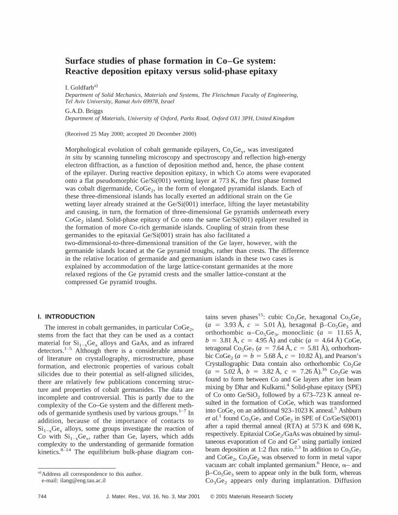
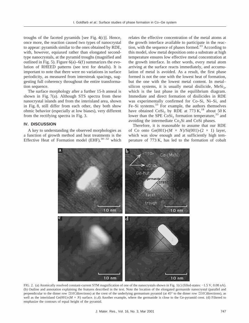
white arrows. Close examination of these nanoprotru-sions (Fig. 2) reveals that they are composed of two dif-ferent types of nanocrystal: elongated ones situateddiagonally (parallel to the⟨110⟩ substrate directions) at the
crests of the underlying pyramidal ones (with the sidesparallel to the⟨100⟩ directions). Hence, the pyramids at thebottom, as outlined in Fig. 2(b) and 2(d), are undoubtedlyGe nanocrystals responsible for most of the zigzag orchevron RHEED pattern. The elongated features at theGe nanocrystal tops, most probably Co-containing ger-manides, were the ones to contribute to the RHEED pat-tern in Fig. 1(c) the four spots at the quarter-orderpositions, marked by black arrows in Fig. 6(c).
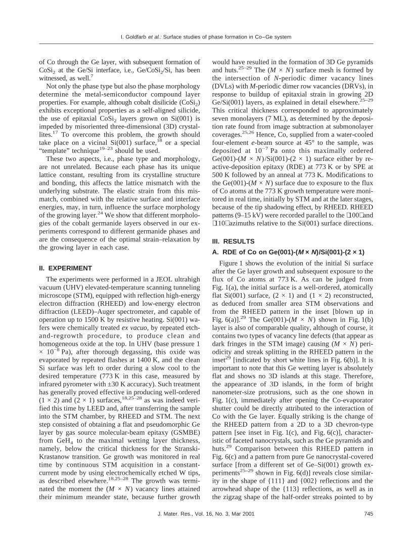
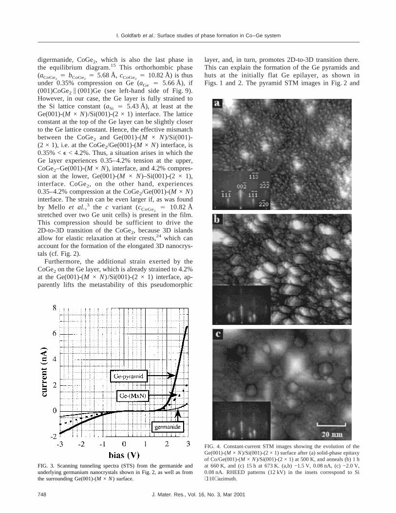
Scanning tunnelingI–V spectra (STS) were then ac-quired from both nanocrystal types, as well as from thesurrounding Ge(001)-(M × N) layer. The results areshown in Fig. 3: although all the spectra exhibit rectify-ing behavior, there are, nevertheless, recognizable differ-ences between them, suggesting the different nature ofthe three substances.
B. Solid-phase epitaxy of Co onGe(001)-(M × N)/Si(001)-(2 × 1)
The Ge(001)-(M × N ) surface with a few germanidenanocrystals on top of Ge pyramids, obtained by RDE ofCo as described in the previous section, served as a sub-strate for the next set of SPE experiments. Although in atypical SPE experiment metal deposition is performed atroom temperature (RT), the temperature for our experi-ment was set to 500 K. On the one hand, it should be toolow to promote phase formation, and on the other hand,sufficiently high to prevent undesired adsorption onto thesample surface, keeping it atomically clean. The latterconsideration is very important, because most STM stud-ies are based on the analysis of surface features, andevery effort should be paid to keep any unrelated and irrel-evant species away from the surface under investigation.Otherwise, some adsorption onto a surface, especially atRT, may take place with time even under UHV conditions.
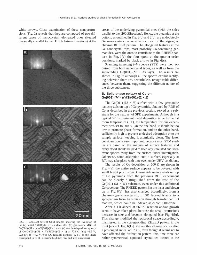
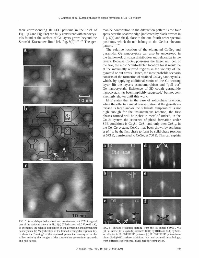
The results of Co deposition at 500 K are shown inFig. 4(a): the entire surface appears to be covered withsmall bright protrusions. Germanide nanocrystals on topof Ge pyramids from the previous RDE experimentcan be clearly distinguished from the rest of theGe(001)-(M × N ) substrate, even under this additionalCo coverage. The RHEED pattern [in the inset and blownup in Fig. 6(e)] has also changed accordingly, from achevron-type characteristic of 3D faceted islands to aspot-pattern from transmission through less-defined 3Dfeatures, which could be indexed as cubic⟨110⟩-zone.
After a 1-h anneal at 660 K, reaction and/or growthseem to have taken place, because the small protrusionsincrease in size and become elongated [see Fig. 4(b)].This change modified the reciprocal space accordingly,manifested in the corresponding RHEED pattern in theinset [also cf. Fig. 6(f)]. Yet another change occurs aftera prolonged anneal at 673 K, even though it seems not tohave affected the diffraction pattern: this time there arerather symmetrical, equiaxed crystallites located at the
FIG. 1. Constant-current STM images showing the evolution ofthe (a) initial Si(001)-(2 × 1) surface after (b) gas source MBE ofGe(001)-(M × N )–Si(001)-(2 × 1) and (c) reactive-deposition epitaxyof Co/Ge(001)-(M × N )/Si(001)-(2 × 1) at 773 K. (a,b) −1.5 V,0.08 nA, (c) −4.0 V, 0.08 nA. RHEED patterns (12 kV) in the insetscorrespond to Si⟨110⟩ azimuth (dimer row and step directions).
I. Goldfarb et al.: Surface studies of phase formation in Co–Ge system
J. Mater. Res., Vol. 16, No. 3, Mar 2001746
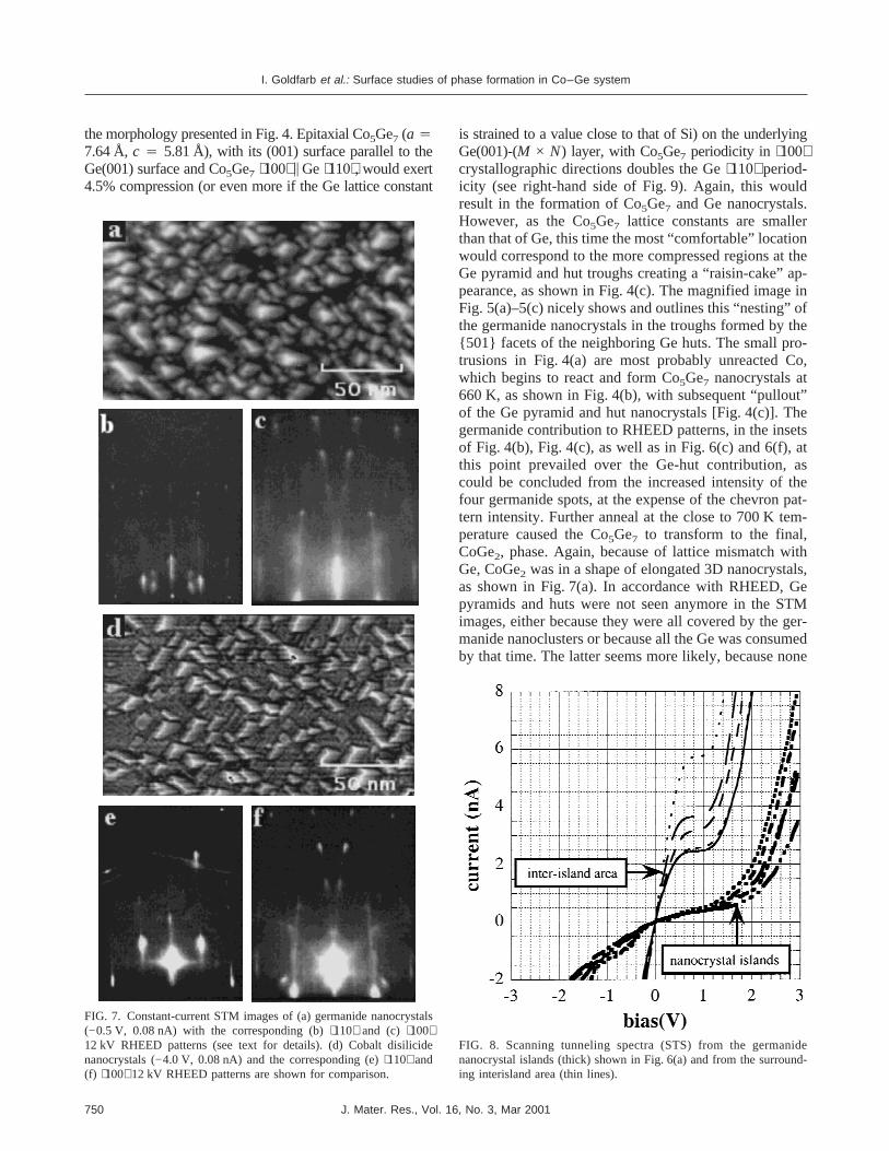
troughs of the faceted pyramids [see Fig. 4(c)]. Hence,once more, the reaction caused two types of nanocrystalto appear: pyramids similar to the ones obtained by RDE,with, however, equiaxed rather than elongated second-type nanocrystals, at the pyramid troughs (magnified andoutlined in Fig. 5). Figure 6(a)–6(f) summarizes the evo-lution of RHEED patterns (see text for details). It isimportant to note that there were no variations in surfaceperiodicity, as measured from interstreak spacings, sug-gesting full coherency throughout the entire transforma-tion sequence.
The surface morphology after a further 15-h anneal isshown in Fig. 7(a). Although STS spectra from thesenanocrystal islands and from the interisland area, shownin Fig. 8, still differ from each other, they both showohmic behavior (especially at low biases), very differentfrom the rectifying spectra in Fig. 3.
IV. DISCUSSION
A key to understanding the observed morphologies asa function of growth method and heat treatments is theEffective Heat of Formation model (EHF),30–32 which
relates the effective concentration of the metal atoms atthe growth interface available to participate in the reac-tion, with the sequence of phases formed.33 According tothis model, slow metal deposition onto a substrate at hightemperature ensures low effective metal concentration atthe growth interface. In other words, every metal atomarriving at the surface reacts immediately, and accumu-lation of metal is avoided. As a result, the first phaseformed is not the one with the lowest heat of formation,but the one with the lowest metal content. In metal–silicon systems, it is usually metal disilicide, MeSi2,which is the last phase in the equilibrium diagram.Immediate and direct formation of disilicides in RDEwas experimentally confirmed for Co–Si, Ni–Si, andFe–Si systems.33 For example, the authors themselveshave obtained CoSi2 by RDE at 773 K,18 about 50 Klower than the SPE CoSi2 formation temperature,33 andavoiding the intermediate Co2Si and CoSi phases.
Therefore, it is reasonable to assume that our RDEof Co onto Ge(001)-(M × N )/Si(001)-(2 × 1) layer,which was slow enough and at sufficiently high tem-perature of 773 K, has led to the formation of cobalt
FIG. 2. (a) Atomically resolved constant-current STM magnification of one of the nanocrystals shown in Fig. 1(c) (filled-states: −1.5 V, 0.08 nA).(b) Outline and annotation explaining the features described in the text. Note the location of the elongated germanide nanocrystal (parallel andperpendicular to the dimer row⟨110⟩ directions) at the crest of the underlying germanium pyramid (at 45° to the dimer row⟨110⟩ directions), aswell as the interisland Ge(001)-(M × N) surface. (c,d) Another example, where the germanide is close to the Ge-pyramid crest. (d) Filtered toemphasize the contours of equal height of the pyramid.
I. Goldfarb et al.: Surface studies of phase formation in Co–Ge system
J. Mater. Res., Vol. 16, No. 3, Mar 2001 747
digermanide, CoGe2, which is also the last phase inthe equilibrium diagram.15 This orthorhombic phase(aCoGe2
4 bCoGe24 5.68 Å, cCoGe2
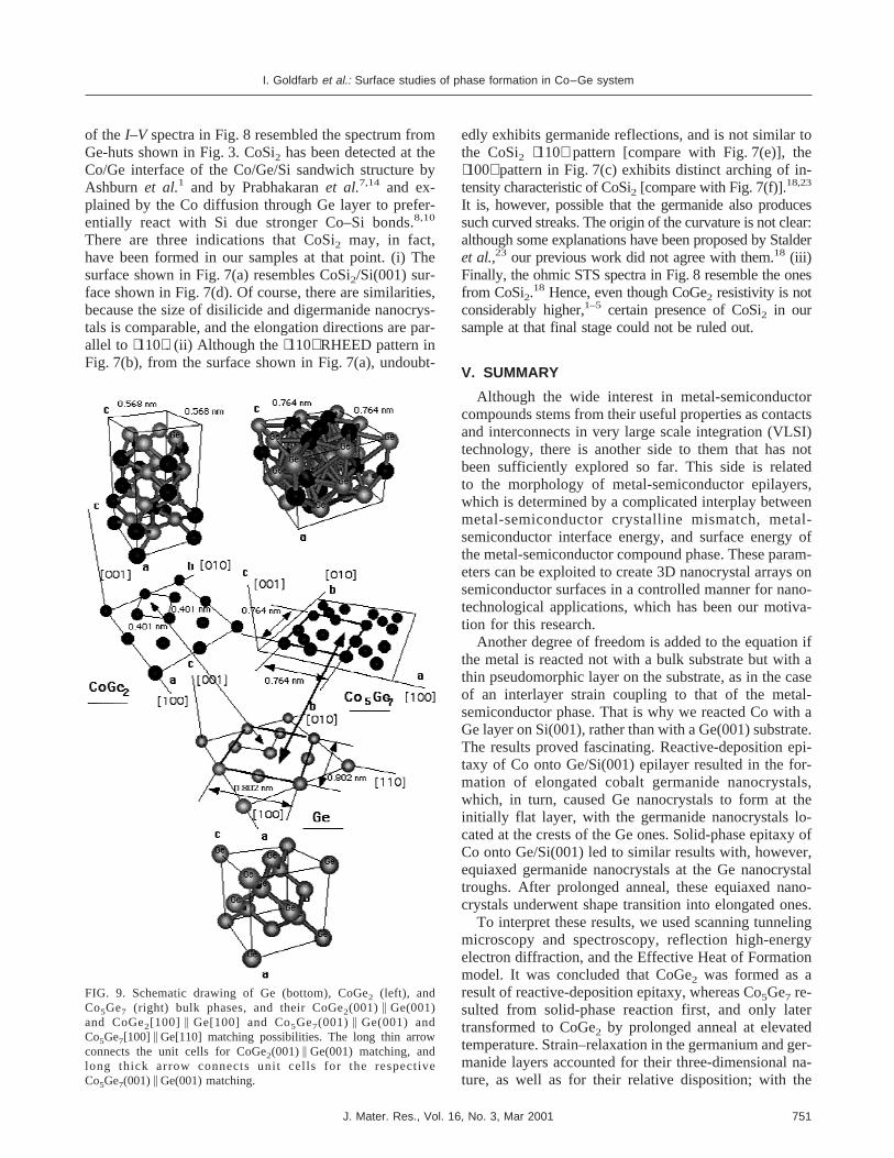
4 10.82 Å) is thusunder 0.35% compression on Ge (aGe 4 5.66 Å), if(001)CoGe2 \ (001)Ge (see left-hand side of Fig. 9).However, in our case, the Ge layer is fully strained tothe Si lattice constant (aSi 4 5.43 Å), at least at theGe(001)-(M × N ) /Si(001)-(2 × 1) interface. The latticeconstant at the top of the Ge layer can be slightly closerto the Ge lattice constant. Hence, the effective mismatchbetween the CoGe2 and Ge(001)-(M × N )/Si(001)-(2 × 1), i.e. at the CoGe2/Ge(001)-(M × N ) interface, is0.35% <e < 4.2%. Thus, a situation arises in which theGe layer experiences 0.35–4.2% tension at the upper,CoGe2–Ge(001)-(M × N ), interface, and 4.2% compres-sion at the lower, Ge(001)-(M × N )–Si(001)-(2 × 1),interface. CoGe2, on the other hand, experiences0.35–4.2% compression at the CoGe2/Ge(001)-(M × N )interface. The strain can be even larger if, as was foundby Mello et al.,3 the c variant (cCoGe2
4 10.82 Åstretched over two Ge unit cells) is present in the film.This compression should be sufficient to drive the2D-to-3D transition of the CoGe2, because 3D islandsallow for elastic relaxation at their crests,24 which canaccount for the formation of the elongated 3D nanocrys-tals (cf. Fig. 2).
Furthermore, the additional strain exerted by theCoGe2 on the Ge layer, which is already strained to 4.2%at the Ge(001)-(M × N ) /Si(001)-(2 × 1) interface, ap-parently lifts the metastability of this pseudomorphic
layer, and, in turn, promotes 2D-to-3D transition there.This can explain the formation of the Ge pyramids andhuts at the initially flat Ge epilayer, as shown inFigs. 1 and 2. The pyramid STM images in Fig. 2 and
FIG. 3. Scanning tunneling spectra (STS) from the germanide andunderlying germanium nanocrystals shown in Fig. 2, as well as fromthe surrounding Ge(001)-(M × N ) surface.
FIG. 4. Constant-current STM images showing the evolution of theGe(001)-(M × N )/Si(001)-(2 × 1) surface after (a) solid-phase epitaxyof Co/Ge(001)-(M × N )/Si(001)-(2 × 1) at 500 K, and anneals (b) 1 hat 660 K, and (c) 15 h at 673 K. (a,b) −1.5 V, 0.08 nA, (c) −2.0 V,0.08 nA. RHEED patterns (12 kV) in the insets correspond to Si⟨110⟩ azimuth.
I. Goldfarb et al.: Surface studies of phase formation in Co–Ge system
J. Mater. Res., Vol. 16, No. 3, Mar 2001748
their corresponding RHEED patterns in the inset ofFig. 1(c) and Fig. 6(c) are fully consistent with nanocrys-tals found at the surface of Ge layers grown beyond theStranski–Krastanow limit [cf. Fig. 6(d)].24–29 The ger-
manide contribution to the diffraction pattern is the fourspots near the shadow edge [indicated by black arrows inFig. 6(c) and 6(f)], close to the one-fourth order spectralpositions, which do not belong to the Ge-hut chevronpattern.27–29
The relative location of the elongated CoGe2 andpyramidal Ge nanocrystals can also be understood inthe framework of strain distribution and relaxation in thelayers. Because CoGe2 possesses the larger unit cell ofthe two, the most “comfortable” location for it would beat the maximally relaxed regions in the vicinity of thepyramid or hut crests. Hence, the most probable scenarioconsists of the formation of strained CoGe2 nanocrystals,which, by applying additional strain on the Ge wettinglayer, lift the layer’s pseudomorphism and “pull out”Ge nanocrystals. Existence of 3D cobalt germanidenanocrystals has been implicitly suggested,7 but not con-vincingly shown until this work.
EHF states that in the case of solid-phase reaction,when the effective metal concentration at the growth in-terface is large and/or the substrate temperature is nothigh enough for the instantaneous reaction, the firstphases formed will be richer in metal.33 Indeed, in theCo–Si system the sequence of phase formation underSPE conditions is Co2Si, CoSi, and only then CoSi2. Inthe Co–Ge system, Co5Ge7 has been shown by Ashburnet al.1 to be the first phase to form by solid-phase reactionat 573 K, transformed to CoGe2 at 700 K. This can explain
FIG. 5. (a–c) Magnified and outlined constant-current STM image ofone of the surfaces shown in Fig. 4(c) (filled-states: −2.0 V, 0.08 nA),to exemplify the relative disposition of the germanide and germaniumnanocrystals. (c) Magnification of the framed rectangular region in (a),to show the “nesting” of the equiaxed germanide nanocrystal at thevalley made by the troughs of the surrounding germanium pyramidsand huts facets.
FIG. 6. Surface evolution starting from the (a) initial Si(001), via(b) flat Ge/Se(001), up to (c) Co/Ge/Si(001) by RDE and (e,f ) by SPE,as reflected in⟨110⟩-RHEED patterns. (d)⟨110⟩-RHEED pattern fromclean Ge/Si(001) surface exhibiting hut and pyramid morphology,from different experiments, given here for comparison.
I. Goldfarb et al.: Surface studies of phase formation in Co–Ge system
J. Mater. Res., Vol. 16, No. 3, Mar 2001 749
the morphology presented in Fig. 4. Epitaxial Co5Ge7 (a 47.64 Å,c 4 5.81 Å), with its (001) surface parallel to theGe(001) surface and Co5Ge7 ⟨100⟩ \ Ge⟨110⟩, would exert4.5% compression (or even more if the Ge lattice constant
is strained to a value close to that of Si) on the underlyingGe(001)-(M × N ) layer, with Co5Ge7 periodicity in ⟨100⟩crystallographic directions doubles the Ge⟨110⟩ period-icity (see right-hand side of Fig. 9). Again, this wouldresult in the formation of Co5Ge7 and Ge nanocrystals.However, as the Co5Ge7 lattice constants are smallerthan that of Ge, this time the most “comfortable” locationwould correspond to the more compressed regions at theGe pyramid and hut troughs creating a “raisin-cake” ap-pearance, as shown in Fig. 4(c). The magnified image inFig. 5(a)–5(c) nicely shows and outlines this “nesting” ofthe germanide nanocrystals in the troughs formed by the{501} facets of the neighboring Ge huts. The small pro-trusions in Fig. 4(a) are most probably unreacted Co,which begins to react and form Co5Ge7 nanocrystals at660 K, as shown in Fig. 4(b), with subsequent “pullout”of the Ge pyramid and hut nanocrystals [Fig. 4(c)]. Thegermanide contribution to RHEED patterns, in the insetsof Fig. 4(b), Fig. 4(c), as well as in Fig. 6(c) and 6(f), atthis point prevailed over the Ge-hut contribution, ascould be concluded from the increased intensity of thefour germanide spots, at the expense of the chevron pat-tern intensity. Further anneal at the close to 700 K tem-perature caused the Co5Ge7 to transform to the final,CoGe2, phase. Again, because of lattice mismatch withGe, CoGe2 was in a shape of elongated 3D nanocrystals,as shown in Fig. 7(a). In accordance with RHEED, Gepyramids and huts were not seen anymore in the STMimages, either because they were all covered by the ger-manide nanoclusters or because all the Ge was consumedby that time. The latter seems more likely, because none
FIG. 7. Constant-current STM images of (a) germanide nanocrystals(−0.5 V, 0.08 nA) with the corresponding (b)⟨110⟩ and (c) ⟨100⟩12 kV RHEED patterns (see text for details). (d) Cobalt disilicidenanocrystals (−4.0 V, 0.08 nA) and the corresponding (e)⟨110⟩ and(f) ⟨100⟩ 12 kV RHEED patterns are shown for comparison.
FIG. 8. Scanning tunneling spectra (STS) from the germanidenanocrystal islands (thick) shown in Fig. 6(a) and from the surround-ing interisland area (thin lines).
I. Goldfarb et al.: Surface studies of phase formation in Co–Ge system
J. Mater. Res., Vol. 16, No. 3, Mar 2001750
of the I–V spectra in Fig. 8 resembled the spectrum fromGe-huts shown in Fig. 3. CoSi2 has been detected at theCo/Ge interface of the Co/Ge/Si sandwich structure byAshburn et al.1 and by Prabhakaranet al.7,14 and ex-plained by the Co diffusion through Ge layer to prefer-entially react with Si due stronger Co–Si bonds.8,10
There are three indications that CoSi2 may, in fact,have been formed in our samples at that point. (i) Thesurface shown in Fig. 7(a) resembles CoSi2/Si(001) sur-face shown in Fig. 7(d). Of course, there are similarities,because the size of disilicide and digermanide nanocrys-tals is comparable, and the elongation directions are par-allel to ⟨110⟩. (ii) Although the⟨110⟩ RHEED pattern inFig. 7(b), from the surface shown in Fig. 7(a), undoubt-
edly exhibits germanide reflections, and is not similar tothe CoSi2 ⟨110⟩ pattern [compare with Fig. 7(e)], the⟨100⟩ pattern in Fig. 7(c) exhibits distinct arching of in-tensity characteristic of CoSi2 [compare with Fig. 7(f)].18,23
It is, however, possible that the germanide also producessuch curved streaks. The origin of the curvature is not clear:although some explanations have been proposed by Stalderet al.,23 our previous work did not agree with them.18 (iii)Finally, the ohmic STS spectra in Fig. 8 resemble the onesfrom CoSi2.
18 Hence, even though CoGe2 resistivity is notconsiderably higher,1–5 certain presence of CoSi2 in oursample at that final stage could not be ruled out.
V. SUMMARY
Although the wide interest in metal-semiconductorcompounds stems from their useful properties as contactsand interconnects in very large scale integration (VLSI)technology, there is another side to them that has notbeen sufficiently explored so far. This side is relatedto the morphology of metal-semiconductor epilayers,which is determined by a complicated interplay betweenmetal-semiconductor crystalline mismatch, metal-semiconductor interface energy, and surface energy ofthe metal-semiconductor compound phase. These param-eters can be exploited to create 3D nanocrystal arrays onsemiconductor surfaces in a controlled manner for nano-technological applications, which has been our motiva-tion for this research.
Another degree of freedom is added to the equation ifthe metal is reacted not with a bulk substrate but with athin pseudomorphic layer on the substrate, as in the caseof an interlayer strain coupling to that of the metal-semiconductor phase. That is why we reacted Co with aGe layer on Si(001), rather than with a Ge(001) substrate.The results proved fascinating. Reactive-deposition epi-taxy of Co onto Ge/Si(001) epilayer resulted in the for-mation of elongated cobalt germanide nanocrystals,which, in turn, caused Ge nanocrystals to form at theinitially flat layer, with the germanide nanocrystals lo-cated at the crests of the Ge ones. Solid-phase epitaxy ofCo onto Ge/Si(001) led to similar results with, however,equiaxed germanide nanocrystals at the Ge nanocrystaltroughs. After prolonged anneal, these equiaxed nano-crystals underwent shape transition into elongated ones.
To interpret these results, we used scanning tunnelingmicroscopy and spectroscopy, reflection high-energyelectron diffraction, and the Effective Heat of Formationmodel. It was concluded that CoGe2 was formed as aresult of reactive-deposition epitaxy, whereas Co5Ge7 re-sulted from solid-phase reaction first, and only latertransformed to CoGe2 by prolonged anneal at elevatedtemperature. Strain–relaxation in the germanium and ger-manide layers accounted for their three-dimensional na-ture, as well as for their relative disposition; with the
FIG. 9. Schematic drawing of Ge (bottom), CoGe2 (left), andCo5Ge7 (right) bulk phases, and their CoGe2(001) \ Ge(001)and CoGe2[100] \ Ge[100] and Co5Ge7(001) \ Ge(001) andCo5Ge7[100] \ Ge[110] matching possibilities. The long thin arrowconnects the unit cells for CoGe2(001) \ Ge(001) matching, andlong thick arrow connects unit cel ls for the respectiveCo5Ge7(001)\ Ge(001) matching.
I. Goldfarb et al.: Surface studies of phase formation in Co–Ge system
J. Mater. Res., Vol. 16, No. 3, Mar 2001 751
smaller-lattice Co5Ge7 at the Ge-hut troughs, and larger-lattice CoGe2 at their crests.
More intense experimental and theoretical efforts arerequired to understand and to model such complex ma-terials systems and processes. For example, advancedequipment with high-spatial resolution and sensitivity,allowing determination of chemical composition of indi-vidual nanocrystals with sufficient precision (so-called“nanoprobes”), is imperative. Because in the meantimethe only information that can be obtained from individualnanocrystalsin situ is scanning tunneling I–V spectros-copy, quantitative interpretation of such spectra can bevery useful, because their derivative is proportional to thedensity of states. However, such an analysis requiresmassive theoretical modeling. Considerable theoreticalefforts, e.g., large-scale thermodynamics and elasticity,are also needed to calculate the energies and strain dis-tribution in relevant layered structures and to model theresultant morphologies, and state-of-the-art diffractionequipment to measure and verify these strains. Neverthe-less, this work shows certain ability to design surfacemorphologies based on strain considerations. The need to“tailor” surface nanostructure is facilitated by future de-vices where nanometer-scale effects will be of para-mount importance.
ACKNOWLEDGMENT
This work is supported by Engineering and PhysicalSciences Research Council grant (EPSRC GR/M54032).
REFERENCES
1. S.P. Ashburn, M.C. O¨ zturk, G. Harris, and D.M. Maher, J. Appl.Phys.74, 4455 (1993).
2. K.E. Mello, S.R. Soss, S.P. Murarka, T-M. Lu, and S.L. Lee,J. Appl. Phys.68, 1817 (1996).
3. K.E. Mello, S.P. Murarka, T-M. Lu, and S.L. Lee, J. Appl. Phys.81, 7261 (1997).
4. S. Dhar and V.N. Kulkarni, Thin Solid Films333,20 (1998).5. Ch. Krontiras, S.N. Georgat, S. Sakkopolous, E. Vitoratos, and
J. Salmi, J. Phys.: Condens. Matter2, 3323 (1990).6. C.S. Lee, I.H. Wilson, W.Y. Cheung, Y.J. Chen, J.B. Xu, and
S.P. Wong, Nucl. Instrum. Methods Phys. Res. Sect. B148, 604(1999).
7. K. Prabhakaran, K. Sumimoto, and T. Ogino, Appl. Phys. Lett.68, 1241 (1996).
8. F. Lin, G. Sarkona, M.K. Hatalis, A.F. Cserhati, E. Austin, andD.W. Greve, Thin Solid Films250,20 (1994).
9. M. Gluck, A. Schuppen, M. Ro¨sler, W. Heinrich, J. Hersener,U. Konig, O. Yam, C. Cytermann, and M. Eizenberg, Thin SolidFilms 290,549 (1995).
10. Z. Wang, D.B. Aldrich, Y.L. Chen, D.E. Sayers, and R.J. Nemanich,Thin Solid Films290,555 (1995).
11. P.T. Goeller, B.I. Boyanov, D.E. Sayers, and R.J. Nemanich, ThinSolid Films320,206 (1998).
12. B.I. Boyanov, P.T. Goeller, D.E. Sayers, and R.J. Nemanich,J. Appl. Phys.86, 1355 (1999).
13. K. Prabhakaran and T. Ogino, Appl. Surf. Sci.121/122, 213(1997).
14. K. Prabhakaran, K. Sumitomo, and T. Ogino, Surf. Sci.421,100(1999).
15. ASM Handbook,Alloy Phase Diagrams(ASM International,The Materials Information Society, 1992), Vol. 3, pp. 2–142;M. Hansen and K. Anderko,Constitution of Binary Alloys(McGraw-Hill, New York, 1958), pp. 475–476.
16. W.B. Pearson,Pearson’s Handbook of Crystallographic Datafor Intermetallic Phases(ASM, Metals Park, Ohio, 1985),pp. 1770–1771.
17. V. Scheuch, B. Voigtla¨nder, and H.P. Bonzel, Surf. Sci.372, 71(1997).
18. I. Goldfarb and G.A.D. Briggs, Phys. Rev. B60, 4800 (1999).19. R.T. Tung, J.M. Gibson, and J.M. Poate, Appl. Phys. Lett.42,888
(1983).20. R.T. Tung and F. Schrey, Appl. Phys. Lett.54, 852 (1989).21. D.P. Adams, S.M. Yalisove, and D.J. Eaglesham, J. Appl. Phys.
76, 5190 (1994).22. V. Buschmann, M. Rodewald, H. Fuess, G. Van Tendeloo, and
C. Scha¨ffer, J. Cryst. Growth191,430 (1998).23. R. Stalder, C. Schwarz, H. Sirringhaus, and H. von Ka¨nel, Surf.
Sci. 291,355 (1992).24. Entire issue no. 4 of the MRS Bull.21, 31 (1996) and references
therein.25. I. Goldfarb, P.T. Hayden, J.H.G. Owen, and G.A.D. Briggs, Phys.
Rev. Lett.78, 3959 (1997).26. I. Goldfarb, P.T. Hayden, J.H.G. Owen, and G.A.D. Briggs, Surf.
Sci. 394,105 (1997).27. I. Goldfarb, J.H.G. Owen, D.R. Bowler, C.M. Goringe, P.T. Hayden,
K. Miki, D.G. Pettifor, and G.A.D. Briggs, J. Vac. Sci. Technol.,A 16, 1938 (1998).
28. I. Goldfarb and G.A.D. Briggs, Recent Res. Dev. Mater. Sci.1,189 (1998).
29. I. Goldfarb and G.A.D. Briggs, Surf. Sci.433–435,449 (1999).30. R. Pretorius, Mater. Res. Soc. Symp. Proc.25, 15 (1984).31. R. Pretorius, A.M. Vredenberg, F.W. Saris, and R. De Reus,
J. Appl. Phys.70, 3636 (1991).32. R. Pretorius, T.K. Marais, and C.C. Theron, Mater. Sci. Eng.,
R 10, 1 (1993).33. A. Vantomme, D. Degroote, J. Decoster, C. Langouche, and
R. Pretorius, Appl. Phys. Lett.74, 3137 (1999).
I. Goldfarb et al.: Surface studies of phase formation in Co–Ge system
J. Mater. Res., Vol. 16, No. 3, Mar 2001752