Embed Size (px)
Citation preview

Surface plasmons in active systems and 2D materials
Marios Mattheakis
September 17, 2015Colloquium at Wesleyan University

I. Introduction to Surface Plasmon Polaritons
II. Active (gain) Dielectrics in Plasmonics
III. Surface Plasmons in 2-Dimensional Materials
IV. Open Issues & Conclusion
Outline

What are plasmonsThe electrons in metals are free to move sustaining collective oscillations with normal modes.
Plasmon is the quantum of free electrons oscillation in a conducting media (plasma oscillation).
Plasmon Polariton is a quasi particle formed by the plasmon-photon coupling.
Surface Plasmon Polaritons are EM surface waves coupled to charge excitations at the surface of metal.

● Beat the diffraction limit (sub-wavelength optics).● Strong localization of EM field (enhanced EM field, nonlinear
optics).● Built extremely small and ultrafast opto-electronic devices
(integrated circuits, plasmonic laser). ● Control electromagnetic energy in subwavelength scales
(nano-waveguides, nano-antennas).● Be high sensitive in dielectric properties (detectors, lenses).
Plasmonics can:
λ sp≪ λphoton

Applications I
1Subwavelength Optics: 150nm slit fabricated in Ag film when illuminated by 488nm laser beam.
Linear Propagation
NonLinear Propagation -Soliton formation-
2,3Nonlinear Optics: 2Plasmon-soliton interaction (Left).3SPP soliton formation (Right).
4Plasmonics Nanoantennas: Antennas with very short wavelength resonance.
5,6Biomolecules detectors: SPPs with surface acoustic waves characterize biomolecules.
1V.A.G. Rivera et al., inTech (2012)2K. Y. Bliokh et. al., Phys. Rev. A 79 (2009)3A.R Davoyan et. al., Opt. Express 17 (2009)
4J. Dorfmuller et al., Nano Lett. 10 (2010)5F. Bender et al., Science and Technology 20 (2009)6 J.M. Friedt et al., J. Appl. Phys. 95 (2004)

Applications II
3,4GRadient INdex lenses (GRIN): Regular dielectrics form plasmonics metaterials lenses.
2Plasmonic Metamaterials: Flat silver-air layers form a plasmonic metasurface providing (left) SPPs with hyperbolic phase fronts and (right) negative refraction.
1L. Huang et al., Nature Communications 4 (2013)2Y. Liu et. al., Appl. Phys. Lett. 14 (2013)
3Y. Liu et. al., Nano Letters 10 (2010)4T. Zentgra et al.,10 Nat. Nanotechnology (2011)
1Optical Holography: Plasmonics meta-surfaces offers 3D optical holography.
✔ Plasmonic solar cells.✔ Plasmonic nanolithography.✔ Plasmonic waveguides.✔ Integrated plasmonic circuits.✔ Plasmonic laser.
●
●
●
...a very promising and various scientific field...

Maxwell Equations
2D
A metal-dielectric interface is located at z = 0
εm
εd
(E⃗B⃗)spp
∼e iqx− k zj|z|
j=(d ,m)
➢ is the SPP wave number
➢
➢ Propagation along x direction
➢ Evanescent along z direction
q
k zj2=q2
−k 02 ε j }
ℜ[εm]<0
k zj2>0⇒q2
>k02 ε j
Metals, semimetals semiconductor
E⃗=(Ex ,0 , E z)
H⃗=(0, H y ,0)
Surface Waves Conditions
A)
B)
C) TM polarizationEM waves
propagating decaying

Drude MetalsDrude model for metals:
εm(ω)=ε h−ωp
2
ω2+iΓω➔ ε
h : high frequency permittivity
➔ ωp: plasma frequency
➔ Γ : metal losses (in freq. units)
SILVER➔ ε
h = 1
➔ ωp= 1.367 1016 Hz
➔ Γ = 1.018 1014 Hz
Loss Function L(ω):
L=−ℑ[ 1ε ]= ℑ[ε ]
|ε|2
Maxima of L show plasmon resonance.SPPs are found before but near to a peak.
ℜ[εm]<0
A useful quantity to determine SPP regime:

Dispersion Relation q(ω):
q (ω)=k 0 √ ε d εm
ε d+εm
Dispersion Relation
λsp= λ0 √ εd+εm
εd εm
SPP wavelength λsp
:
SubWavelengthλ
sp<λ
0
Α
B
CΑ. Bound Modes
B. Quasi-Bound Modes
C. Radiative Modes
εm<−ε d<0
−εd<εm<0
q : Real k
z: : Imaginary
εm>0
q : Imaginary k
z: : Imaginary
q : Real k
z: : Real
k 0=ωc
=2π cλ0
k p=ω p
c

SPPs excitation
1SA Maier. Plasmonics: Fundamentals and applications. Plasmonics: Fundamentals and Applications (2007).
Near Field1 method used for excitation of SPPs:
A point source with R=20nm located d=100nm above the metal surface acts as a point source since λ<<R.
Monochromatic TM EM source with λ=345nm.Silica glass is used as dielectric with ε
d=1.69.
Silver is used as metal at f=870THz.
R, λ
d
λ0
λsp
=1.6
SubWavelengthOptics
εm=−5.24+i 0.12
ε d=1.69
COMSOL simulation

Lossy propagation
εm(ω)=ε 1m+iε2m εm(ω)=ε h−ω p
2
ω2+Γ 2
+iω p
2 Γ
ω3+ωΓ 2
Metal's permittivity is a complex function
METALLOSSES
Drude Model
Resulting to complex q and lossy SPPs propagation
q (ω)=q1+ iq2
Propagation length
LI=1
ℑ[q]
The rate of change of the SPP EM energy attenuation
Point Source x-location

Active (gain) dielectrics● Dielectrics with complex permittivity ε
d = ε
1d + iε
2d (ε
1d > 0) and
complex refractive index n = nr + iκ (ε
d = n2 ).
● The imaginary part accounts for gain (in opposite to metal losses).● Gain materials counterbalance metal losses resulting to:
Enhanced SPP EM intensity I. Larger penetration length. Longer SPPs propagation length L
I.
metal
dielectricinterface
M. Mattheakis et al. Expert from the Proceedings of the 2014 COMSOL conference in Cambridge (2014).

Lossless SPPs propagationQ.
Is there any gain ε2d for which SPPs propagate without losses?
ℑ[q]=0 ⇒ LI→∞
This gain satisfies the PT symmetry
nSP=qk 0
=√ εd εm
εd+εm
PT Symmetry
nSP= n̄SP
n(−x )= n̄(x )Trivial case of PT symmetry
Effective SPP refractive index
}
A.Yes . It is given by the solution of equation: ℑ[q(ε2d )]=0
ε2d=ε PTn
PT is real
nPT
spatial independent

Gain Overcomes Losses
εPT=|εm|
2
2 ε2m (1−√1−(2 ε1d ε2m
|εm|2 )
2
)εPT<ε1d √ |εm|
2
ε 1d ε1m
−1≡εc
ε 2d=εPT
Limits of PT symmetry and of lossless SPPs propagation
εPT<ε c
εPT>ε c
PT symmetry andLossLess SPP propagation.
Broken PT symmetry and prohibited SPP propagation.
real q
imag q
Complex SPP wave number q: q=q1+iq2
Demand q2=0:
Demand q1=real:ε
PT and ε
c are given in
terms of the optical properties of the interface.
M. Mattheakis et al., arXiv:1507.08167

Lossless SPPs propagation
SPPs dispersion relation under PT symmetry.➔ Interchange between real
and imaginary part of q at ε
PT=ε
c
SPPs COMSOL simulations.➔ Lossy SPPs propagation
ε2d
=0 (up)➔ Lossless SPPs propagation
ε2d
=εPT
(down)
M. Mattheakis et al., arXiv:1507.08167

Gain SaturationA steep phase transition is expected to propagation length SPPs L
I
Because of the sudden interchange in imaginary part of q.
Loss
less
SPP
s
prop
agat
ion NO
SPP
s mod
es.
Qua
si-bo
und
mode
s
M. Mattheakis et al., arXiv:1507.08167

Main Result
So,An active (gain) metamaterial, with the desirable frequency-dependent dielectric function (εPT), may be designed for the fabrication of PT symmetric plasmonic systems, providing infinite SPPs propagation for any surface plasmon eigen-frequencies.
M. Mattheakis et al., arXiv:1507.08167

SPPs in ultra-thin layers
q (ω)=k 0
ε 1+ε2
1−εm
Assume an ultra thin metallic film of thickness d 0, sandwiched by two dielectrics with ε
1 and ε
2. ε
1
ε2
εm
1,2Dispersion Relation q(ω):
k 0=ωc
Case with same dielectrics (ε1=ε
2=ε
d)
q (ω)=k 0
2 εd
1−εm
1M. Jablan et al. Proceeding of the IEEE, 101 7 (2013)
These dispersion relations should be useful for studying plasmons in 2D materials.
1,2A very good approximation near to plasmon resonance, where q>>k
0
2T. Low et al. Phys. Rev. Lettof, 113 (2014)

Two Dimensional Materials
The Flatland is real !!!The Flatland is real !!!● 2D Materials2D Materials are crystalline materials
consisting of few layers of atoms.● In 2D materials the width d is much smaller
than the other dimensions, the width is less than 1nm!!!
● The properties are dramatically changing when we are going from 3D to 2D.
d < 1nm
GrapheneGraphene is an atomically thick (d=0.32nm) sheet honeycomb lattice of carbon atoms.
➔ It is hundreds of times stronger than steel.➔ It has the largest thermal and electrical
conductivity that is known.➔ It supports plasmon modes with very short
wavelength.

Ab initio Calculations
Permittivity ε is calculated by first principles, i.e. by solving quantum mechanics equations.
Density Functional Theory (DFT) is a computational quantum mechanical modeling method for investigating the electronic structure.
Walter Kohn chemistry Nobel prize 1998

Graphene
Dispersion Relation q(ω) and Loss function:
Graphene has negative permittivity for a small regime, so we expect to support surface plasmons.
Graphene permittivity obtained by DFT
Air is used as enviroment ε1=ε
2=1
A small negative ε regime, with high losses (Im[ε]).
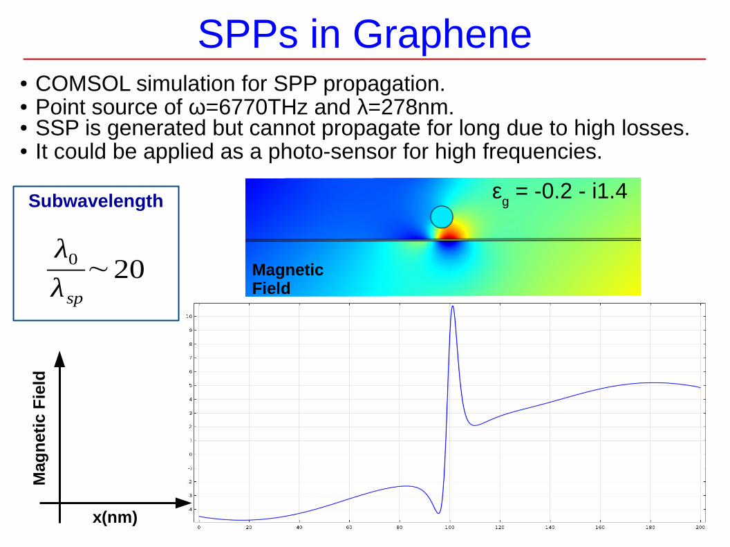
SPPs in Graphene● COMSOL simulation for SPP propagation.● Point source of ω=6770ΤHz and λ=278nm.● SSP is generated but cannot propagate for long due to high losses.● It could be applied as a photo-sensor for high frequencies.
Subwavelength
λ0
λsp
∼20
x(nm)
Mag
net
ic F
ield
Magnetic Field
εg = -0.2 - i1.4

Doping materials● With doping we add electrons to the conduction band or remove
from the valence band. As a result, the conductivity of the material is increased, because more electrons can move free.
● The doping can be performed by chemical reactions or by applying external voltage.
● It is a way to use semi-conductors for plasmonics.
k
E
● The amount of doping controls the plasmon resonace frequency.controls the plasmon resonace frequency.More doping leads to higher plasmon frequency and vice versa.

Doped GrapheneDoped graphene shows a new plasmon resonance, at lower frequency.
● New plasmon resonance at lower frequency. ● The new plasmon resonance frequency can
be tuned by the amount of doping.
Preliminary Results

SPPs in Doped Graphene● COMSOL simulation for SPP propagation.● The doped graphene layer of thickness d=0.33nm surrounded by air.● A point EM source is located 3nm above the graphene layer. The
source is monochromatic with ω=300THz and λ=6.3μm. ● The magnetic field is illustrated showing the SPP propagation
x
z
HPreliminary Results
εg = -40 - i0.3

Graphene and subwavelength optics
● COMSOL simulation for SPP propagation.● Magnetic field on the graphene surface.
x(nm)
Mag
net
ic F
ield
Extreme small
wavelength!
λ0
λsp
=900
Preliminary Results

More Configurations
Graphene is splitting and rejoining SPPs
R=10nm
Graphene sheet as SPPs waveguide and splitter

Two Graphene layers
New plasmonics modes arise in a system of two layers of graphene.
Wang et al., Appl. Phys. Lett. 100 (2012)

Results
● Graphene is a great material for doing subwavelength optics.● Graphene supports plasmons in several frequencies.● Graphene offers SPP near to optical frequencies.● SPP spectrum can be tuned by doping amount.● Graphene can be used as SPP nano-waveguides.● It is a great material for designing of integrated nano circuits.● More SPP modes arise in multilayer of graphene.

Open Issues
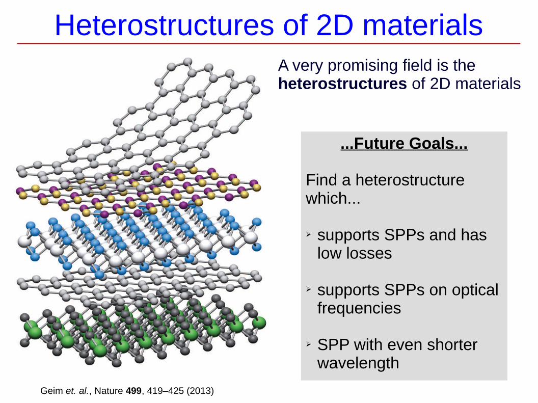
Heterostructures of 2D materials
...Future Goals...
Find a heterostructure which...
➢ supports SPPs and has low losses
➢ supports SPPs on optical frequencies
➢ SPP with even shorter wavelength
Geim et. al., Nature 499, 419–425 (2013)
A very promising field is the heterostructures of 2D materials

Quantum PlasmonicsQuantum plasmonics1 has been studied the last years revealing a lot of quantum properties.
● Interaction or/and coupled with other quasi particles➔ Plasmon-Phonon2 interaction➔ Plasmon-Exciton Interaction3 (Plexciton)➔ Plasmon-Plasmon4 Interaction➔ Plasmon decays to phonons5
➔ Phonons decay to plasmons5
● Quantum Information Theory➔ Plasmonic Entaglement6
● Quantum Plasmonic Metamaterials7,8
1M.S. Tame et al., Nature Physics 9 (2013)2V. B. Brar et. al., Nano. Lett. 10 (2014)3A. Manjavacas et. al., Nano. Lett. 11 (2011)4Y.A. Akimov et. al., Nanotech. 23 (2012)
5V.H. Nguyen et al., Nanosci. Nanotech. 6 (2015)6J.S. Fakonas et. al., Nat. Phot. 8 (2014)7N. Papasimakis et. al., Opt. Express 18 (2010)8J. Cheng et. al., Nano. Lett. 14 (2014)

Conclusion● Surface Plasmon Polaritons (SPPs) are EM surface waves
coupled to charge excitations at the surface of a conductors.➔ Dispersion Relation and SPP wavelength.➔ SPPs provide nano scale exploration (subwavelength optics).
● Active or Gain materials.➔ Enhance SPPs propagation.➔ PT symmetry in plasmonic systems.➔ Lossless and prohibited SPP propagation.
● Two Dimensional materials, graphene.➔ Graphene supports plasmons at high frequencies.➔ Doped graphene and new plasmonic resonance.➔ Even smaller SPP wavelength.➔ Graphene as SPP waveguide, cloak and splitter.
● Heterostructures of 2D materials and Quantum plasmonics.

Thank you for your attention!
Collaborators● Prof. George Tsironis, University of Crete, Greece.● Prof. Efthimios Kaxiras, Harvard University, USA.● Prof. Mario Molina, University of Chile, Santiago.● Prof. Thomas Oikonomou, Nazarbayev University, Kazakstan.● Dr. Sharmila Shirodkar, Harvard University, USA.
[email protected]://scholar.harvard.edu/marios_matthaiakis


![INVITED PAPER PlasmonsinGraphene: …soljacic/graphene_Proceedings_IEEE.pdf · Polarization of graphene and plasmons under strain have been investigated in [54] and [55]. Plasmons](https://img.pdfslide.us/doc/110x75/5ae4b30d7f8b9ae1578b4a90/invited-paper-plasmonsingraphene-soljacicgrapheneproceedingsieeepdfpolarization.jpg)