Embed Size (px)
Citation preview
Plasmons govern the high frequency optical properties of materials since they
determine resonances in the dielectric function ε(ω) and hence in the refraction
index
Often written as for non ferromagnetic materials.
Above the plasma frequency, electric fields penetrate into the matter which
becomes therefore transparent to electromagnetic radiation (ultraviolet
transparency of alkali metals).
Surface plasmons determine the high frequency surface response function,
governing the screening of external fields and electron transmission at the
interface, determining e.g. photoemission intensities.
)()()( n
Plasmons, Surface Plasmons and Plasmonics
Plasmons exist also for nearly 2-dimensional systems, formed e.g. in charge
inversion layers and artificially layered materials [1]. Such 2D plasmons may
have low energy and govern many dynamical processes involving electrons and
phonons and mediate the formation of Cooper pairs in superconductors [2]
[1] M.H. March and M.P. Tosi, Adv. in Physics 44, 299 (1995)
[2] J. Ruvalds, Nature 328, 299 (1987)
)()( n
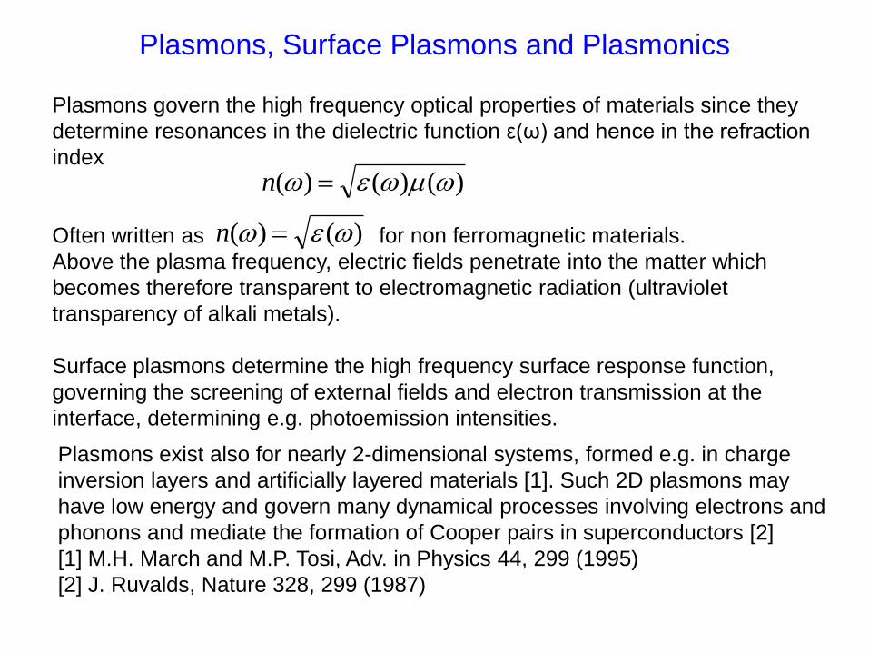
Surface response function and
photoemission:
Cl on Si and Ge
Conclusion a top adsorption for Si
and hollow site for Ge!
quite counterintuitive, but possible ...
Subsequent EXAFS and
NEXAFS investigations
indicate identical site
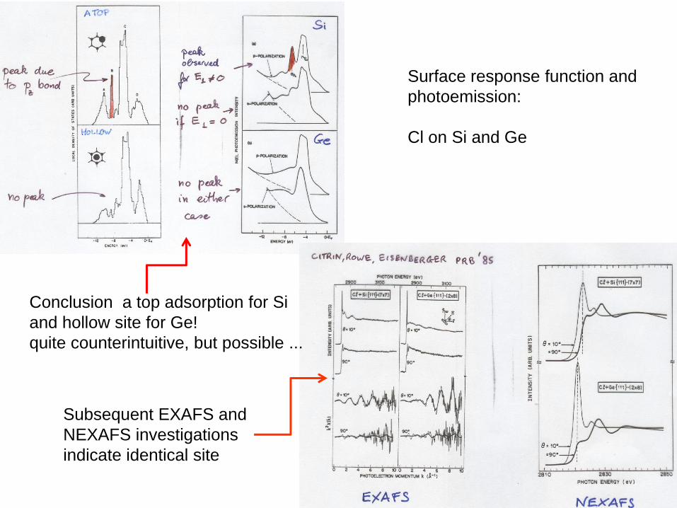
Plasmons and Surface plasmons:
collective excited states of the 3D electron gas
Equation of motion for a free electron of mass m and charge e in presence of a
time varying electric field E=E(t) :
eEdt
xdm
2
2ti
oeEE ti
oexx
2m
eEx o
o Em
neP
2
2
EEm
neD
)()41(
2
2
For ε=0 → E≠0 also when D=0 , i.e. when there are no external charges.
ε=0 determines therefore the condition for which self sustaining polarization waves
can exist at the frequency
m
nep
22 4
2
2
1
pFor the free electron gas it follows:
and the polarization reads
while the electric displacement field is:
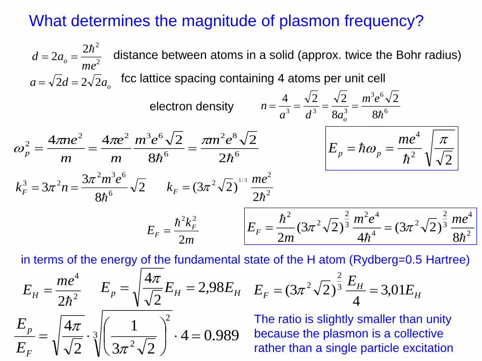
What determines the magnitude of plasmon frequency?
2
222
mead o
oada 222
6
63
333 8
2
8
224
em
adan
o
6
82
6
63222
2
2
8
244
emem
m
e
m
nep
28
33
6
63223
emnkF
2
22
2)23(
3/1
mekF
2
4
3
2
2
4
42
3
2
22
8)23(
4)23(
2
meem
mEF
22
4
meE pp
in terms of the energy of the fundamental state of the H atom (Rydberg=0.5 Hartree)
2
4
2
meEH HHp EEE 98,2
2
4
H
HF E
EE 01,3
4)23( 3
2
2
989.0423
1
2
43
2
2
F
p
E
E
distance between atoms in a solid (approx. twice the Bohr radius)
electron density
fcc lattice spacing containing 4 atoms per unit cell
m
kE F
F2
22
The ratio is slightly smaller than unity
because the plasmon is a collective
rather than a single particle excitation
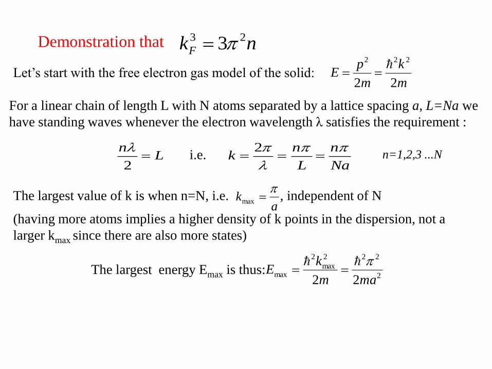
Demonstration that nkF
23 3
Let’s start with the free electron gas model of the solid: m
k
m
pE
22
222
For a linear chain of length L with N atoms separated by a lattice spacing a, L=Na we
have standing waves whenever the electron wavelength λ satisfies the requirement :
Ln
2
Na
n
L
nk
2
The largest value of k is when n=N, i.e. , independent of N
(having more atoms implies a higher density of k points in the dispersion, not a
larger kmax since there are also more states)
ak
max
2
222
max
2
max22 mam
kE
i.e. n=1,2,3 ...N
The largest energy Emax is thus:
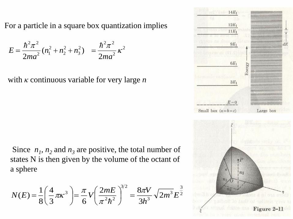
Since n1, n2 and n3 are positive, the total number of
states N is then given by the volume of the octant of
a sphere
with κ continuous variable for very large n
2
2
22
2
ma
)(
2
2
3
2
2
2
12
22
nnnma
E
For a particle in a square box quantization implies
2
3
3
3
23
22
3 23
82
63
4
8
1)( Em
h
VmEVEN
2
3
3
3
23
22
3 23
82
63
4
8
1)( Em
h
VmEVEN
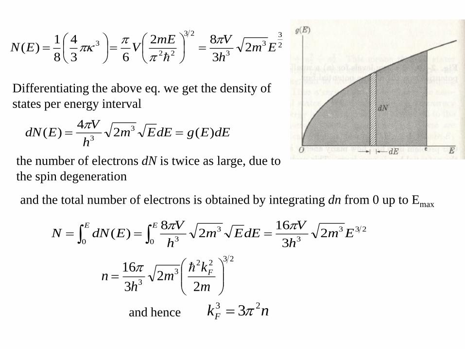
dEEgdEEmh
VEdN )(2
4)( 3
3
Differentiating the above eq. we get the density of
states per energy interval
the number of electrons dN is twice as large, due to
the spin degeneration
and the total number of electrons is obtained by integrating dn from 0 up to Emax
EE
Emh
VdEEm
h
VEdNN
0
233
3
3
302
3
162
8)(
2322
3
3 22
3
16
m
km
hn F
nkF
23 3and hence
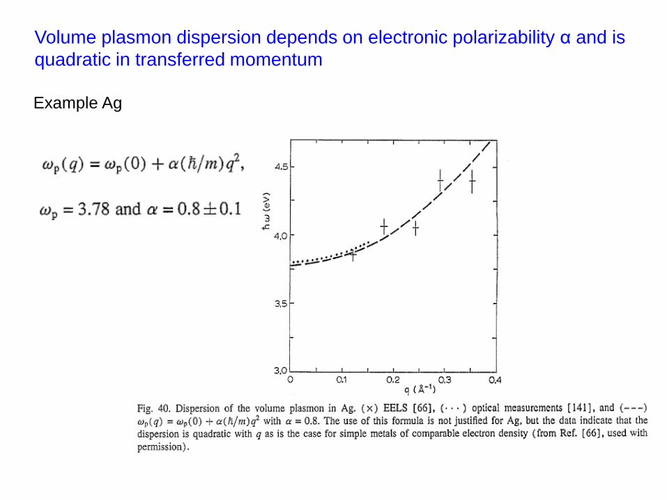
Volume plasmon dispersion depends on electronic polarizability α and is
quadratic in transferred momentum
Example Ag
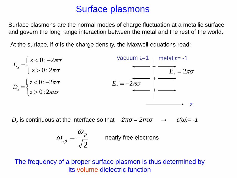
At the surface, if σ is the charge density, the Maxwell equations read:
2:0
2:0
z
zEz
2:0
2:0
z
zDz
Dz is continuous at the interface so that -2πσ = 2πεσ → ε(ω)= -1
nearly free electrons
2
p
sp
Surface plasmons
Surface plasmons are the normal modes of charge fluctuation at a metallic surface
and govern the long range interaction between the metal and the rest of the world.
The frequency of a proper surface plasmon is thus determined by
its volume dielectric function
vacuum ε=1 metal ε= -1
2zE
2zE
z
+
+
+
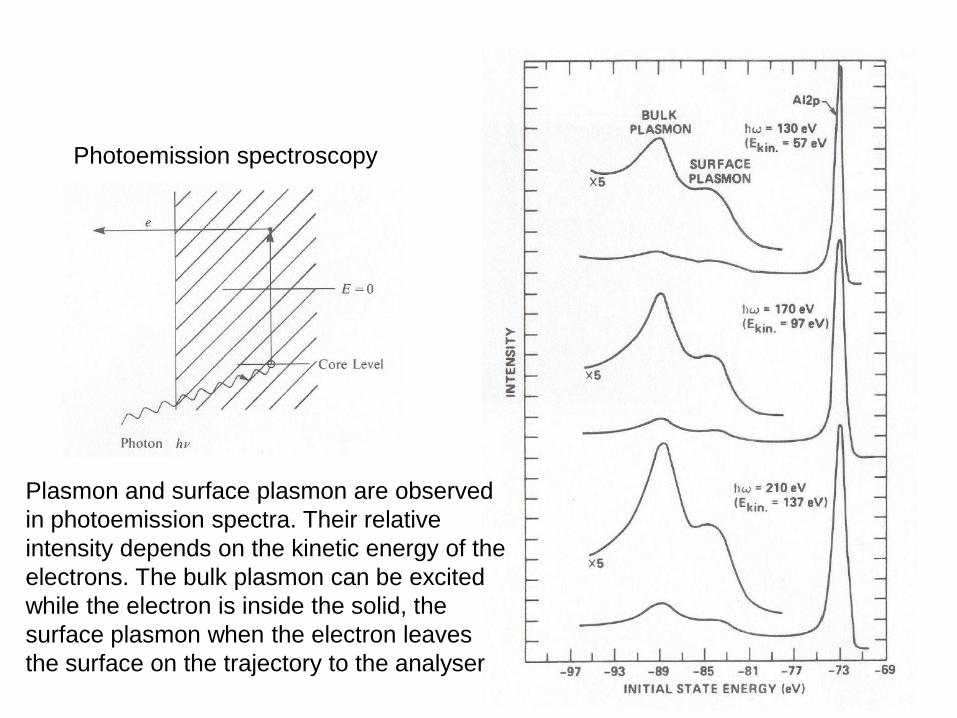
Photoemission spectroscopy
Plasmon and surface plasmon are observed
in photoemission spectra. Their relative
intensity depends on the kinetic energy of the
electrons. The bulk plasmon can be excited
while the electron is inside the solid, the
surface plasmon when the electron leaves
the surface on the trajectory to the analyser
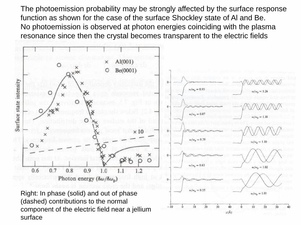
The photoemission probability may be strongly affected by the surface response
function as shown for the case of the surface Shockley state of Al and Be.
No photoemission is observed at photon energies coinciding with the plasma
resonance since then the crystal becomes transparent to the electric fields
Right: In phase (solid) and out of phase
(dashed) contributions to the normal
component of the electric field near a jellium
surface
))())((2
11)(0()( 2
|||||| qoqddq spsp
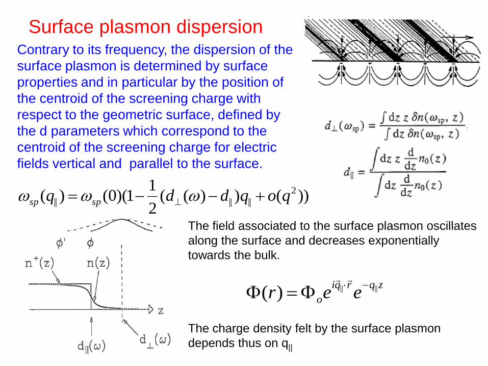
Contrary to its frequency, the dispersion of the
surface plasmon is determined by surface
properties and in particular by the position of
the centroid of the screening charge with
respect to the geometric surface, defined by
the d parameters which correspond to the
centroid of the screening charge for electric
fields vertical and parallel to the surface.
Surface plasmon dispersion
The field associated to the surface plasmon oscillates
along the surface and decreases exponentially
towards the bulk.
The charge density felt by the surface plasmon
depends thus on q||
zqrqi
o eer ||||)(
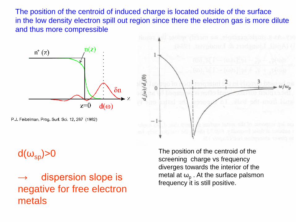
The position of the centroid of induced charge is located outside of the surface
in the low density electron spill out region since there the electron gas is more dilute
and thus more compressible
d(ωsp)>0
→ dispersion slope is
negative for free electron
metals
The position of the centroid of the
screening charge vs frequency
diverges towards the interior of the
metal at ωp . At the surface palsmon
frequency it is still positive.
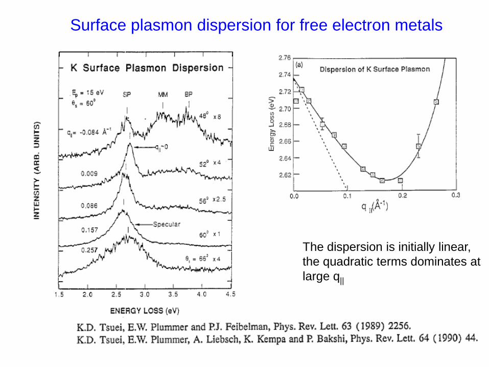
Surface plasmon dispersion for free electron metals
The dispersion is initially linear,
the quadratic terms dominates at
large q||
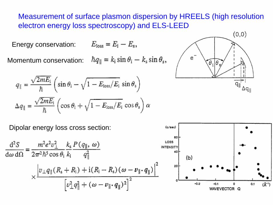
Measurement of surface plasmon dispersion by HREELS (high resolution
electron energy loss spectroscopy) and ELS-LEED
Energy conservation:
Momentum conservation:
Dipolar energy loss cross section:
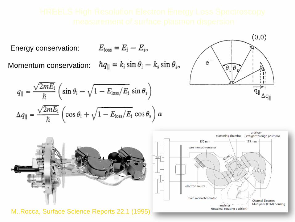
HREELS High Resolution Electron Energy Loss Spectroscopy
measurement of surface plasmon dispersion
Energy conservation:
Momentum conservation:
M..Rocca, Surface Science Reports 22,1 (1995)
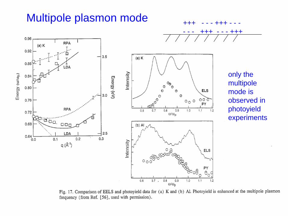
Multipole plasmon mode +++ - - - +++ - - -
- - - +++ - - - +++
only the
multipole
mode is
observed in
photoyield
experiments
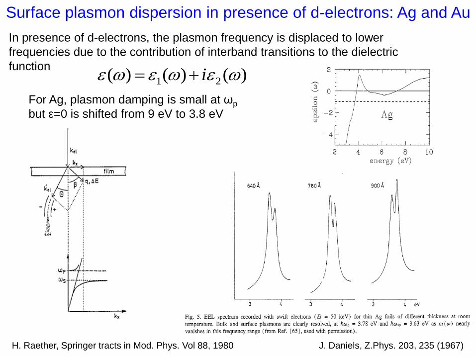
In presence of d-electrons, the plasmon frequency is displaced to lower
frequencies due to the contribution of interband transitions to the dielectric
function )()()( 21 i
For Ag, plasmon damping is small at ωp
but ε=0 is shifted from 9 eV to 3.8 eV
H. Raether, Springer tracts in Mod. Phys. Vol 88, 1980 J. Daniels, Z.Phys. 203, 235 (1967)
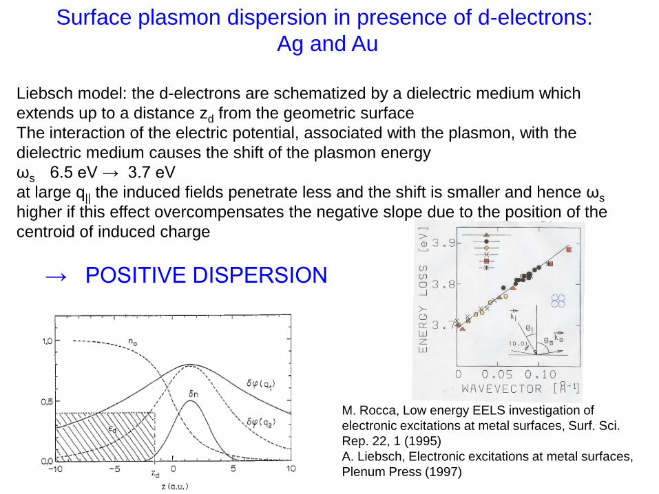
Surface plasmon dispersion in presence of d-electrons: Ag and Au
Surface plasmon dispersion in presence of d-electrons:
Ag and Au
Liebsch model: the d-electrons are schematized by a dielectric medium which
extends up to a distance zd from the geometric surface
The interaction of the electric potential, associated with the plasmon, with the
dielectric medium causes the shift of the plasmon energy
ωs 6.5 eV → 3.7 eV
at large q|| the induced fields penetrate less and the shift is smaller and hence ωs
higher if this effect overcompensates the negative slope due to the position of the
centroid of induced charge
→ POSITIVE DISPERSION
M. Rocca, Low energy EELS investigation of
electronic excitations at metal surfaces, Surf. Sci.
Rep. 22, 1 (1995)
A. Liebsch, Electronic excitations at metal surfaces,
Plenum Press (1997)
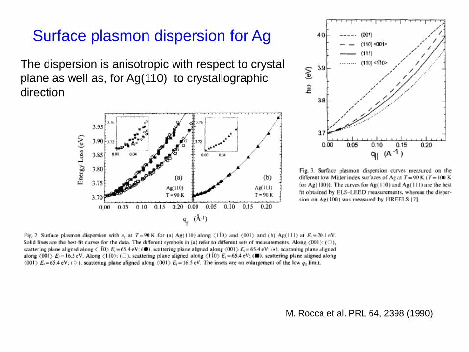
Surface plasmon dispersion for Ag
M. Rocca et al. PRL 64, 2398 (1990)
The dispersion is anisotropic with respect to crystal
plane as well as, for Ag(110) to crystallographic
direction
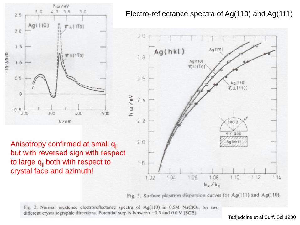
Electro-reflectance spectra of Ag(110) and Ag(111)
Anisotropy confirmed at small q||
but with reversed sign with respect
to large q|| both with respect to
crystal face and azimuth!
Tadjeddine et al Surf. Sci 1980
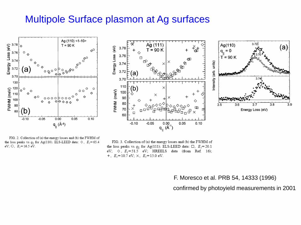
Multipole Surface plasmon at Ag surfaces
F. Moresco et al. PRB 54, 14333 (1996)
confirmed by photoyield measurements in 2001
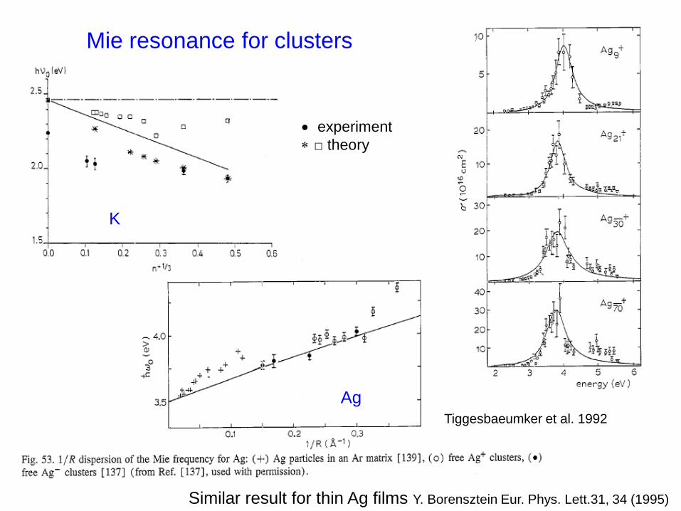
Mie resonance for clusters
K
Ag
experiment
□ theory
Similar result for thin Ag films Y. Borensztein Eur. Phys. Lett.31, 34 (1995)
Tiggesbaeumker et al. 1992
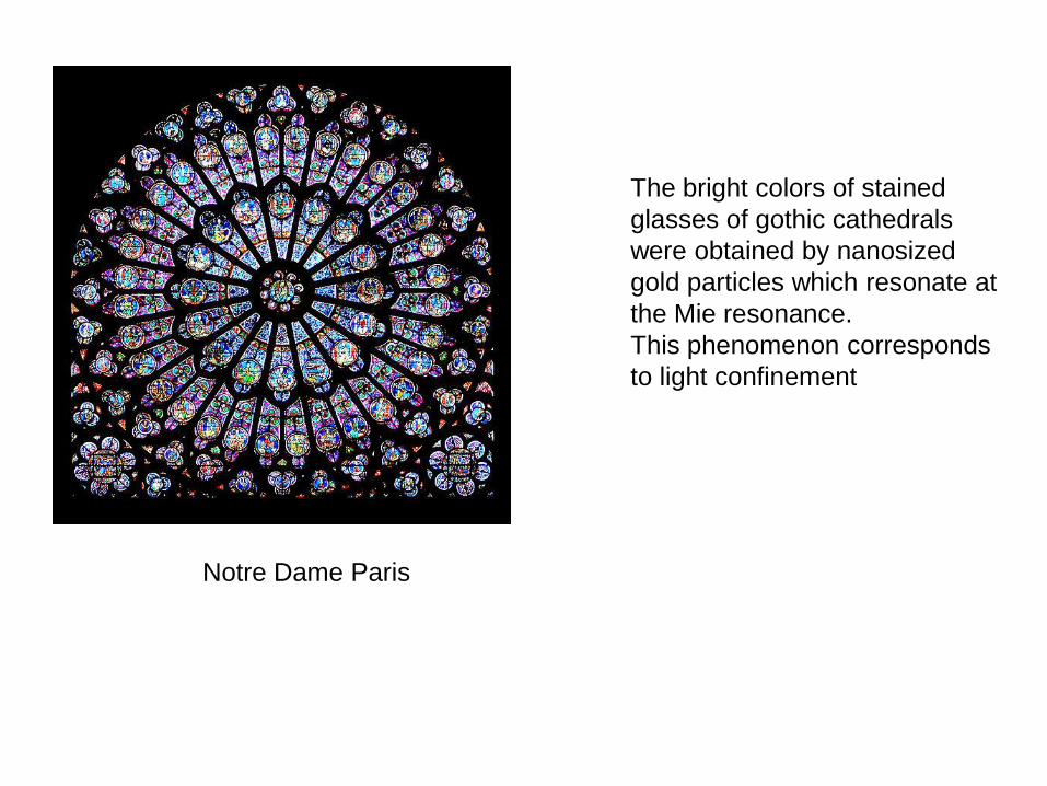
The bright colors of stained
glasses of gothic cathedrals
were obtained by nanosized
gold particles which resonate at
the Mie resonance.
This phenomenon corresponds
to light confinement
Notre Dame Paris
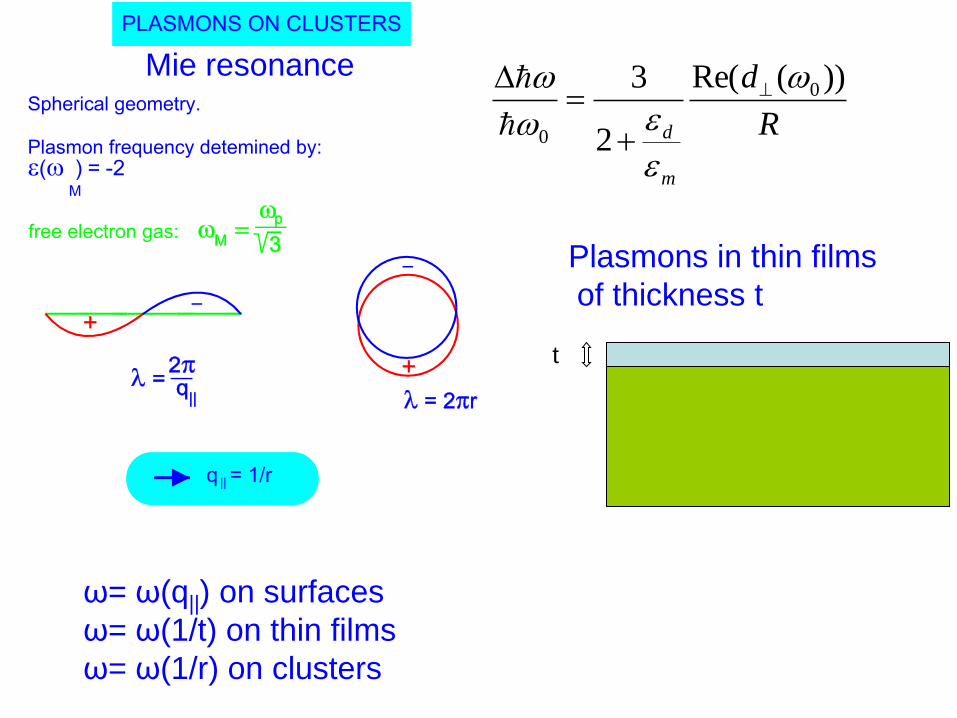
ω= ω(q||) on surfaces
ω= ω(1/t) on thin films
ω= ω(1/r) on clusters
Mie resonance
t
Plasmons in thin films
of thickness t
R
d
m
d
))(Re(
2
3 0
0
t
thin films of thickness t
εd
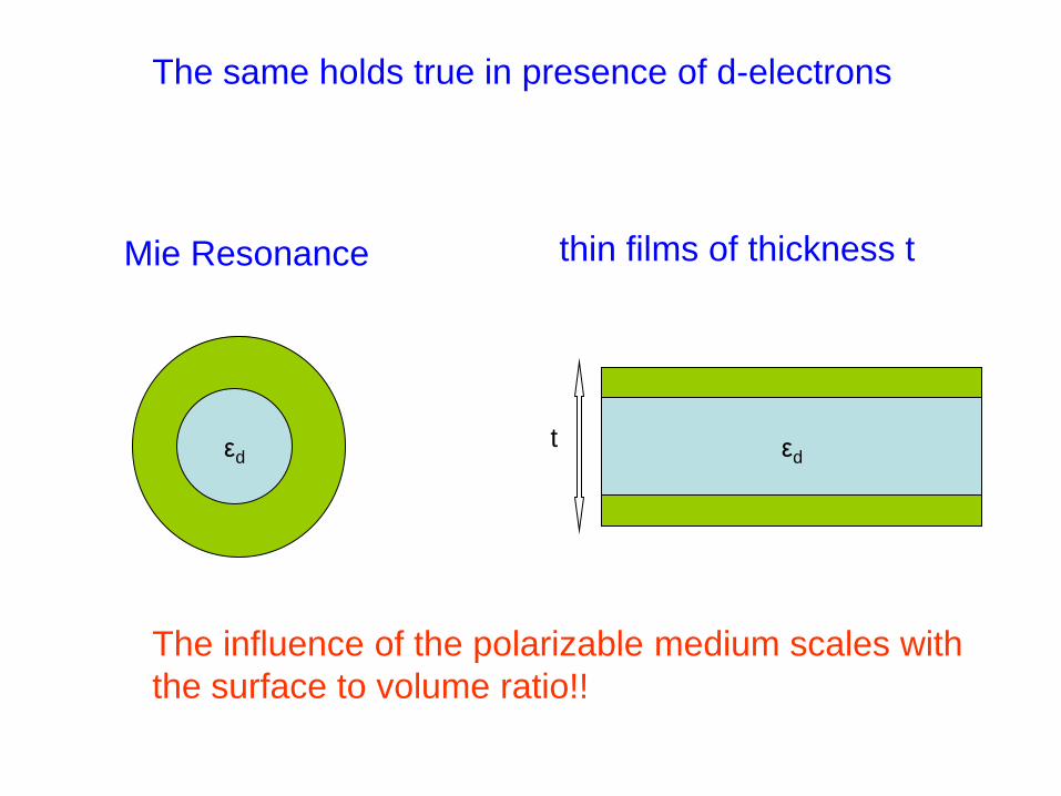
The same holds true in presence of d-electrons
εd
The influence of the polarizable medium scales with
the surface to volume ratio!!
Mie Resonance
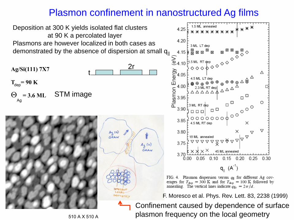
Plasmon confinement in nanostructured Ag films
t 2r
F. Moresco et al. Phys. Rev. Lett. 83, 2238 (1999)
Deposition at 300 K yields isolated flat clusters
at 90 K a percolated layer
Plasmons are however localized in both cases as
demonstrated by the absence of dispersion at small q||
STM image
Confinement caused by dependence of surface
plasmon frequency on the local geometry
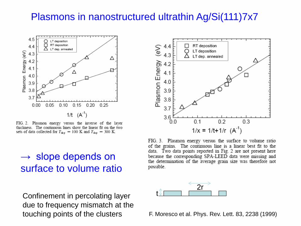
Plasmons in nanostructured ultrathin Ag/Si(111)7x7
→ slope depends on
surface to volume ratio
t 2r
F. Moresco et al. Phys. Rev. Lett. 83, 2238 (1999)
Confinement in percolating layer
due to frequency mismatch at the
touching points of the clusters
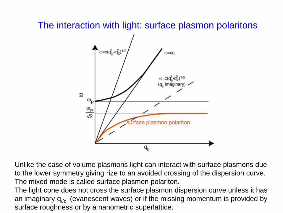
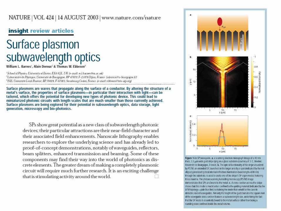
The interaction with light: surface plasmon polaritons
Unlike the case of volume plasmons light can interact with surface plasmons due
to the lower symmetry giving rize to an avoided crossing of the dispersion curve.
The mixed mode is called surface plasmon polariton.
The light cone does not cross the surface plasmon dispersion curve unless it has
an imaginary q//z (evanescent waves) or if the missing momentum is provided by
surface roughness or by a nanometric superlattice.
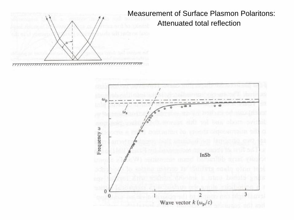
Attenuated total reflection
Measurement of Surface Plasmon Polaritons:
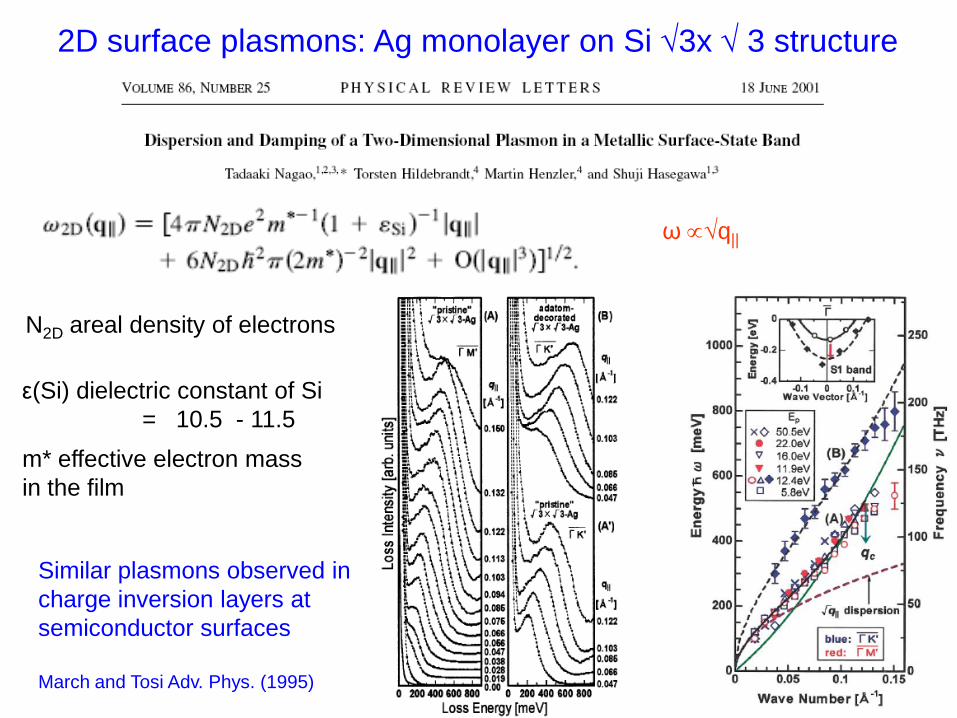
2D surface plasmons: Ag monolayer on Si 3x 3 structure
N2D areal density of electrons
ε(Si) dielectric constant of Si
= 10.5 - 11.5
m* effective electron mass
in the film
ω q||
Similar plasmons observed in
charge inversion layers at
semiconductor surfaces
March and Tosi Adv. Phys. (1995)
2D surface plasmons: Ag monolayer on Si 3x 3 structure
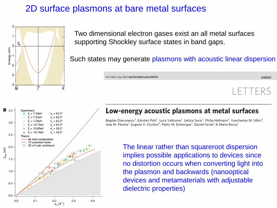
Two dimensional electron gases exist an all metal surfaces
supporting Shockley surface states in band gaps.
2D surface plasmons at bare metal surfaces
Such states may generate plasmons with acoustic linear dispersion
The linear rather than squareroot dispersion
implies possible applications to devices since
no distortion occurs when converting light into
the plasmon and backwards (nanooptical
devices and metamaterials with adjustable
dielectric properties)
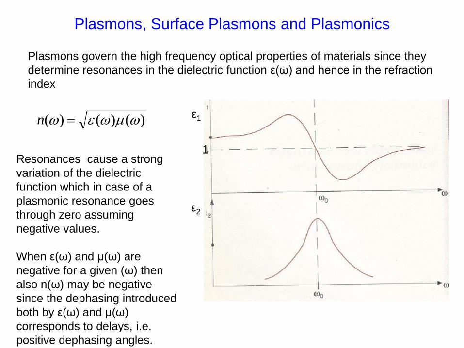
Plasmons govern the high frequency optical properties of materials since they
determine resonances in the dielectric function ε(ω) and hence in the refraction
index
)()()( n
Plasmons, Surface Plasmons and Plasmonics
ε1
ε2
1 Resonances cause a strong
variation of the dielectric
function which in case of a
plasmonic resonance goes
through zero assuming
negative values.
When ε(ω) and μ(ω) are
negative for a given (ω) then
also n(ω) may be negative
since the dephasing introduced
both by ε(ω) and μ(ω)
corresponds to delays, i.e.
positive dephasing angles.
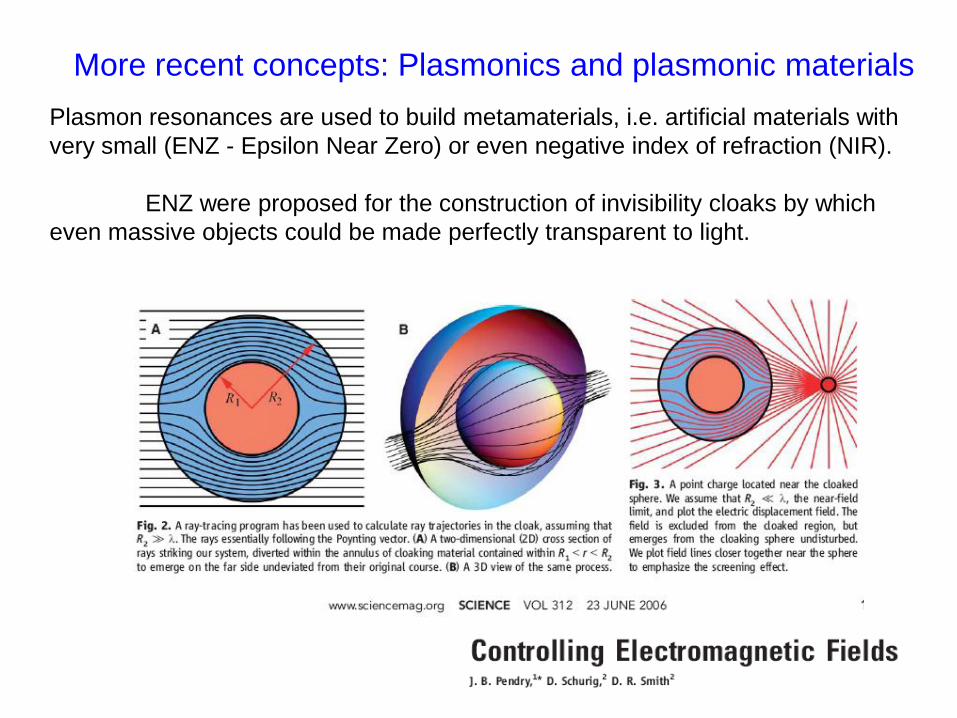
More recent concepts: Plasmonics and plasmonic materials
Plasmon resonances are used to build metamaterials, i.e. artificial materials with
very small (ENZ - Epsilon Near Zero) or even negative index of refraction (NIR).
ENZ were proposed for the construction of invisibility cloaks by which
even massive objects could be made perfectly transparent to light.
R. A. Shelby et al., Science 292, 77 -79 (2001)
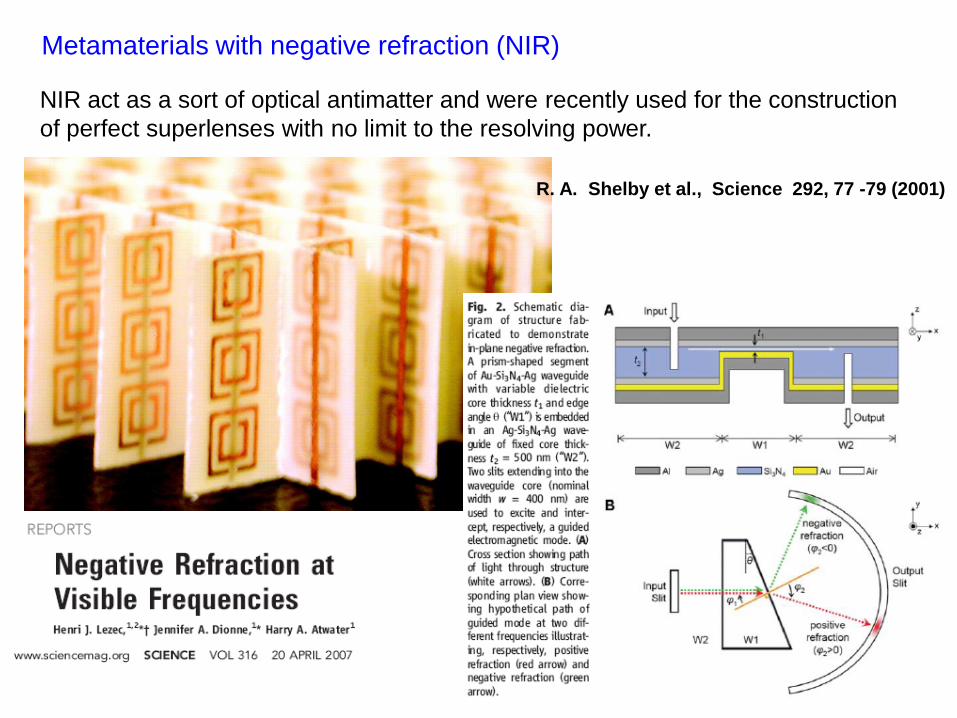
Metamaterials with negative refraction (NIR)
NIR act as a sort of optical antimatter and were recently used for the construction
of perfect superlenses with no limit to the resolving power.
To keep in mind
Surface plasmons control the high frequency optical response of materials.
For usual 3D surface plasmons, the frequency is a bulk property, but the
dispersion is determined by the surface electronic structure. The dispersion is
then negative for simple metals and positive for d-metals. At very small
wavevectors the dispersion cuts the light cone giving rise to surface plasmon
polaritons.
For clusters surface plasmons correspond to the Mie resonance showing the
same properties vs inverse cluster size. For thin film the surface plasmon
frequency scales with inverse film thickness.
Surface plasmons exist also for 2D electron gases and are then acoustic with
squareroot like dispersion. For intrinsic two dimensional surface states the
interaction with the underlying electron gas implies a surface plasmon with
acoustic linear dispersion which can couple with light via surface roughness or
surface nanostructures and looks promising for applications
Further reading:
• M. Rocca, “Low energy EELS investigation of surface electronic
excitations”, Surf. Sci. Rep. 22, 1 (1995)
• A. Liebsch, “Excitations at metal surfaces” (Plenum Press London (1977))
• J. Pendry, “Playing tricks with light”, Science 285, 1687 (1999)
• Subsequent Science and Nature articles 1999-2007