Embed Size (px)
Citation preview
Dynamic Article LinksC<Energy &Environmental Science
Cite this: Energy Environ. Sci., 2011, 4, 3646
www.rsc.org/ees PAPER
Publ
ishe
d on
29
July
201
1. D
ownl
oade
d by
St.
Pete
rsbu
rg S
tate
Uni
vers
ity o
n 13
/02/
2014
10:
37:0
9.
View Article Online / Journal Homepage / Table of Contents for this issue
Surface and subsurface morphology of operating nanowire:fullerene solar cellsrevealed by photoconductive-AFM†
Wing C. Tsoi,ab Patrick G. Nicholson,a Jong Soo Kim,b Debdulal Roy,a Tim L. Burnett,a Craig E. Murphy,a
Jenny Nelson,b Donal D. C. Bradley,b Ji-Seon Kim*b and Fernando A. Castro*a
Received 13th June 2011, Accepted 11th July 2011
DOI: 10.1039/c1ee01944a
The 3D nanometer scale phase separated morphology of organic solar cells crucially affects
performance. We demonstrate that photoconductive atomic force microscopy can provide both surface
and subsurface information in operating organic solar cells providing direct correlation between 3D
filmmorphology, local nanoscale optoelectronic properties and device characteristics. P3HT nanowire:
PCBM bulk-heterojunction working devices were investigated. The macroscopic solar cell performance
improvements upon thermal annealing, such as an increase in the short circuit current, the open circuit
voltage and the fill factor, are consistent with observed enrichment of PCBM at the air interface and
increased nanowire crystallinity. PC-AFM is able to directly resolve the associated changes in charge
transport and collection at the local scale, with an estimated depth resolution of at least 20 nm inside the
film.
1. Introduction
Power conversion efficiency of organic solar cells (OPVs) has
recently overcome the 8% barrier.1 A major driving force in the
development of the field has been the growing understanding of
the complex but crucial effect of the 3D nanometre scale
morphology on device efficiency.2–4 The morphological require-
ments for an optimal device include the formation of a large
surface area between the electron donor and electron acceptor
components, with domain sizes in the few nanometers range to
aNational Physical Laboratory (NPL), Teddington, Middlesex, TW110LW, United Kingdom. E-mail: [email protected] of Physics & Centre for Plastic Electronics, Imperial CollegeLondon, London, SW7 2AZ, United Kingdom. E-mail: [email protected]
† Electronic supplementary information (ESI) available. See DOI:10.1039/c1ee01944a
Broader context
Polymer/fullerene thin films exhibiting phase separation on the nano
in organic solar cells. It is now clear that the arrangement of donor a
and needs to be controlled in order to allow high efficient solar cells
processing and post processing parameters in a complex way. Ther
devices to avoid change in morphology due to differences in pr
measurement methods over the last decades, there is no technique
with nanoscale resolution at the same time. The work presented her
that photoconductive AFM can provide subsurface information at
correlation between nanoscale film morphology and device charact
3646 | Energy Environ. Sci., 2011, 4, 3646–3651
maximize charge generation, whilst having percolated paths in
the donor and the acceptor phases to ensure loss-free charge
collection at the anode and cathode electrodes, respectively.2,3
However, controlling film morphology is challenging and,
unfortunately, there are no techniques so far that can charac-
terise the 3D nanoscale domain structure and optoelectronic
properties at the same time in operating device conditions.2
In the last decade the morphology of thin films has been
investigated by several methods,2 including electron tomog-
raphy,5 cross-sectional electron microscopy,6 secondary ion mass
spectroscopy,7 near-edge X-ray absorption fine structure,8 X-ray
photoelectron spectroscopy,9 small angle neutron scattering,10
and grazing incidence X-ray difraction.11 Though these tech-
niques are ideal for revealing structural and crystallographic
information, they do not provide optoelectronic information. In
parallel, scanning probe microscopies have been used to probe
both structural and electrical information at the nanoscale via
metre scale have attracted widespread interest as the active layer
nd acceptor phases in the film strongly affects device behaviour
to be developed. The 3D film morphology depends on material,
efore characterisation should ideally be made in real operating
ocessing conditions. Despite intensive development of novel
today that allows morphological and electrical characterisation
e represents a significant step in this direction. We demonstrate
least 20 nm inside the 80 nm thick active layer, providing direct
eristics.
This journal is ª The Royal Society of Chemistry 2011
Publ
ishe
d on
29
July
201
1. D
ownl
oade
d by
St.
Pete
rsbu
rg S
tate
Uni
vers
ity o
n 13
/02/
2014
10:
37:0
9.
View Article Online
surface 2D mapping.2,12 In this work we show that photocon-
ductive atomic force microscopy (PC-AFM) can provide both
surface and subsurface information in operating organic solar
cells providing direct correlation between 3D film morphology,
local nanoscale optoelectronic properties and device
characteristics.
PC-AFM is a promising recent variant of AFM, where
a conductive probe in contact-mode is used to simultaneously
measure the topography and the photocurrent generated by
a sample under illumination. Being reported for the first time in
1999,13 it started to receive significant attention from 2007
following publications by Ginger’s group where they demon-
strated 2D mapping of nanoscale photocurrent generation and
local electrical characteristics in different polymer:fullerene
systems, including poly(3-butylthiophene) nanowire:phenyl-
C61-butyric acid methyl ester (PCBM) blends.14–16 The group of
T.-Q. Nguyen reported PC-AFM studies of small molecule:
fullerene devices17 as well as adding a tunable light source to their
setup allowing the determination of local incident photon-to-
electron conversion efficiency.18 Moreover, recently NIST has
published PC-AFM results on variations in photoresponse in
poly(3-hexylthiophene) (P3HT):PCBM films19 where they
concluded that the observed inhomogeneities are due to local
variations at the surface, not reflecting the 3D arrangement
throughout the film. In fact, in common with most scanning
probe microscopies, non-destructive approaches have restricted
this method to the investigation of local surface variations.
In contrast, we demonstrate here that PC-AFM indeed can
provide subsurface morphological and electrical information and
clearly show the distribution of donor and acceptor phases
within a blend, allowing a direct correlation of local nanoscale
properties with macroscopic device characteristics. As a sample
of interest we used bulk-heterojunction solar cells with PCBM
and P3HT nanowires as electron acceptor and electron donor,
respectively. There is a growing interest in the use of semi-
conducting polymer nanowires for a number of applications,20
including photovoltaics. These wires are partially crystalline
which improves charge transport21 and, in principle, by adjusting
the width and density of the wires it should be possible to
maximise charge generation. At the same time, the large wire
length (�hundreds nm) facilitates percolation of charges through
the device reducing series resistance.20
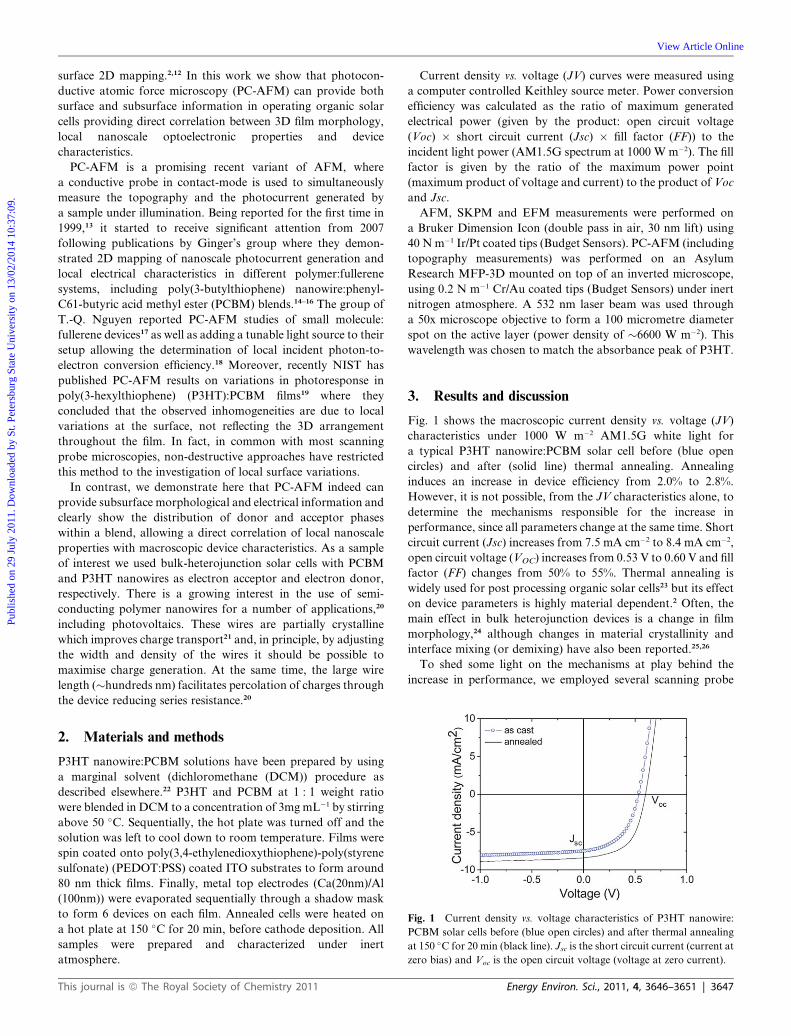
Fig. 1 Current density vs. voltage characteristics of P3HT nanowire:
PCBM solar cells before (blue open circles) and after thermal annealing
at 150 �C for 20 min (black line). Jsc is the short circuit current (current at
zero bias) and Voc is the open circuit voltage (voltage at zero current).
2. Materials and methods
P3HT nanowire:PCBM solutions have been prepared by using
a marginal solvent (dichloromethane (DCM)) procedure as
described elsewhere.22 P3HT and PCBM at 1 : 1 weight ratio
were blended in DCM to a concentration of 3mgmL�1 by stirring
above 50 �C. Sequentially, the hot plate was turned off and the
solution was left to cool down to room temperature. Films were
spin coated onto poly(3,4-ethylenedioxythiophene)-poly(styrene
sulfonate) (PEDOT:PSS) coated ITO substrates to form around
80 nm thick films. Finally, metal top electrodes (Ca(20nm)/Al
(100nm)) were evaporated sequentially through a shadow mask
to form 6 devices on each film. Annealed cells were heated on
a hot plate at 150 �C for 20 min, before cathode deposition. All
samples were prepared and characterized under inert
atmosphere.
This journal is ª The Royal Society of Chemistry 2011
Current density vs. voltage (JV) curves were measured using
a computer controlled Keithley source meter. Power conversion
efficiency was calculated as the ratio of maximum generated
electrical power (given by the product: open circuit voltage
(Voc) � short circuit current (Jsc) � fill factor (FF)) to the
incident light power (AM1.5G spectrum at 1000 W m�2). The fill
factor is given by the ratio of the maximum power point
(maximum product of voltage and current) to the product of Voc
and Jsc.
AFM, SKPM and EFM measurements were performed on
a Bruker Dimension Icon (double pass in air, 30 nm lift) using
40 Nm�1 Ir/Pt coated tips (Budget Sensors). PC-AFM (including
topography measurements) was performed on an Asylum
Research MFP-3D mounted on top of an inverted microscope,
using 0.2 N m�1 Cr/Au coated tips (Budget Sensors) under inert
nitrogen atmosphere. A 532 nm laser beam was used through
a 50x microscope objective to form a 100 micrometre diameter
spot on the active layer (power density of �6600 W m�2). This
wavelength was chosen to match the absorbance peak of P3HT.
3. Results and discussion
Fig. 1 shows the macroscopic current density vs. voltage (JV)
characteristics under 1000 W m�2 AM1.5G white light for
a typical P3HT nanowire:PCBM solar cell before (blue open
circles) and after (solid line) thermal annealing. Annealing
induces an increase in device efficiency from 2.0% to 2.8%.
However, it is not possible, from the JV characteristics alone, to
determine the mechanisms responsible for the increase in
performance, since all parameters change at the same time. Short
circuit current (Jsc) increases from 7.5 mA cm�2 to 8.4 mA cm�2,
open circuit voltage (VOC) increases from 0.53 V to 0.60 V and fill
factor (FF) changes from 50% to 55%. Thermal annealing is
widely used for post processing organic solar cells23 but its effect
on device parameters is highly material dependent.2 Often, the
main effect in bulk heterojunction devices is a change in film
morphology,24 although changes in material crystallinity and
interface mixing (or demixing) have also been reported.25,26
To shed some light on the mechanisms at play behind the
increase in performance, we employed several scanning probe
Energy Environ. Sci., 2011, 4, 3646–3651 | 3647
Publ
ishe
d on
29
July
201
1. D
ownl
oade
d by
St.
Pete
rsbu
rg S
tate
Uni
vers
ity o
n 13
/02/
2014
10:
37:0
9.
View Article Online
microscopies to investigate the morphology and electrical prop-
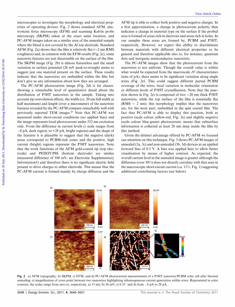
erties of operating devices. Fig. 2 shows standard AFM, elec-
trostatic force microscopy (EFM) and scanning Kelvin probe
microscopy (SKPM) taken at the exact same location, and
PC-AFM images taken on a similar area of the annealed sample
where the blend is not covered by the Al top electrode. Standard
AFM (Fig. 2a) shows that the film is relatively flat (�2 nm RMS
roughness) and, in common with the EFM results (Fig. 2c), some
nanowire features are just discernable on the surface of the film.
The SKPM image (Fig. 2b) is almost featureless and the small
variation in surface potential (26 mV peak-to-trough) seems to
suggest just one material present on the surface. These results
indicate that the nanowires are embedded within the film but
don’t give us any information about how they are arranged.
The PC-AFM photocurrent image (Fig. 2d) is far clearer,
showing a remarkable level of quantitative detail about the
distribution of P3HT nanowires in the sample. Taking into
account tip convolution effects, the width (ca. 20 nm full width at
half maximum) and length (over a micrometer) of the nanowire
features revealed by the PC-AFM compare remarkably well with
previously reported TEM images.27 Note that PC-AFM was
measured under short-circuit conditions (no applied bias) and
the image represents local photocurrent under 532 nm excitation
only. From the difference in current levels (z scale ranges from
�8 pA, dark region, to +28 pA, bright regions) and the shape of
the features it is plausible to suggest that the negative (dark)
areas correspond to PCBM-rich zones and the positive, high
current (bright) regions represent the P3HT nanowires. Note
that the work functions of the AFM gold-coated tip (top elec-
trode) and PEDOT:PSS (bottom electrode) are similar
(measured difference of 100 mV, see Electronic Supplementary
Information†) and therefore there is no significant electric field
present to drive charges to either electrode. This means that the
PC-AFM current is formed mainly by charge diffusion and the
Fig. 2 a) AFM topography, b) SKPM, c) EFM, and d) PC-AFM photocu
annealing; e) magnification of cross point between two nanowires highlightin
contrast, the scales range from zero to, respectively, a) 15 nm; b) 26 mV; c) 0
3648 | Energy Environ. Sci., 2011, 4, 3646–3651
AFM tip is able to collect both positive and negative charges. In
a first approximation, a change in photocurrent polarity then
indicates a change in material type on the surface if the probed
area is formed of areas rich in electrons and areas rich in holes. In
our samples these areas are formed by, PCBM and P3HT,
respectively. However, we expect this ability to discriminate
between materials with different electrical properties to be
general and therefore applicable also to, for instance, quantum
dots and inorganic semiconductor nanowires.
The PC-AFM images show that the photocurrent from the
nanowires is not uniform. Though the overall value is within
what would be expected from the macroscale JV characteristics
(tens of pA), there seems to be significant variation along single
wires (Fig. 2e). This could suggest different partial PCBM
coverage of the wires, local variation in molecular orientation
or different levels of P3HT crystallisation. Note that the junc-
tion shown in Fig. 2e) is composed of two �20 nm thick P3HT
nanowires, while the top surface of the film is essentially flat
(RMS � 2 nm); this morphology implies that the nanowires
are, for the most part, embedded in the spin coated film. The
fact that PC-AFM is able to display this junction, both as
positive (scale colour yellow-red, Fig. 2e) and slightly negative
(scale colour blue-green) photocurrent, means that subsurface
information is collected at least 20 nm deep inside the film by
this method.
Given the distinct advantage offered by PC-AFM we focused
our attention on this technique. Fig. 3 shows PC-AFM images of
annealed (3a, 3c) and non-annealed (3b, 3d) devices at an applied
forward bias of 0.5 V. A bias was applied here to allow better
visualisation by means of higher contrast. As expected, the
overall current level in the annealed image is greater although the
difference (over 50%) does not directly correlate with that seen in
the macroscopic short-circuit current (ca. 11%, Fig. 1) suggesting
additional contributing factors (see below).
rrent measurements of a P3HT nanowire:PCBM solar cell after thermal
g inhomogeneous current generation within wires. Represented in color
.31� and d) from �8 pA to 28 pA.
This journal is ª The Royal Society of Chemistry 2011
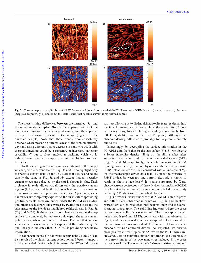
Fig. 3 Current map at an applied bias of +0.5V for annealed (a) and not annealed (b) P3HT nanowire:PCBM blends. c) and d) are exactly the same
images as, respectively, a) and b) but the scale is such that negative current is represented in blue.
Publ
ishe
d on
29
July
201
1. D
ownl
oade
d by
St.
Pete
rsbu
rg S
tate
Uni
vers
ity o
n 13
/02/
2014
10:
37:0
9.
View Article Online
The most striking differences between the annealed (3a) and
the non-annealed samples (3b) are the apparent width of the
nanowires (narrower for the annealed sample) and the apparent
density of nanowires present in the image (higher for the
annealed sample). Note that these trends were consistently
observed when measuring different areas of the film, on different
days and using different tips. A decrease in nanowire width with
thermal annealing could be a signature of increased nanowire
crystallinity27 due to closer molecular packing, which would
induce better charge transport leading to higher Jsc and
better FF.
To further investigate the information contained in the images
we changed the current scale of Fig. 3a and 3b to highlight only
the positive current (Fig. 3c and 3d). Note that Fig. 3c and 3d are
exactly the same as Fig. 3a and 3b, except that all negative
current (electrons collected by the tip) is shown in blue. Such
a change in scale allows visualising only the positive current
regions (holes collected by the tip), which should be a signature
of nanowires directly exposed on the surface. Apparently, some
nanowires are completely exposed to the air interface (providing
positive current), some are buried under the PCBM-rich matrix
and others are just partially covered by PCBM-rich areas (at the
subsurface of the blend) as highlighted (white circles) in Fig. 3a
(3b) and 3c(3d). If the wire was completely exposed at the top
surface (or completely buried) we would expect the same current
polarity everywhere, as discussed above. The fact that we can
visualise nanowires that are not exposed at the surface (Fig. 3a
and 3b) again indicates that PC-AFM is providing subsurface
information.
The apparent increase in nanowire density (Fig. 3a and 3b) can
be a result of the higher current generation and better transport
in the annealed device, which increases the PC-AFM image
This journal is ª The Royal Society of Chemistry 2011
contrast allowing us to distinguish nanowire features deeper into
the film. However, we cannot exclude the possibility of more
nanowires being formed during annealing (presumably from
P3HT crystallites within the PCBM phase) although the
observed density difference is probably too large to be entirely
due to this.
Interestingly, by decoupling the surface information in the
PC-AFM data from that of the subsurface (Fig. 3), we observe
a lower nanowire density (48%) on the film surface after
annealing when compared to the non-annealed device (50%)
(Fig. 3c and 3d, respectively). A similar increase in PCBM
coverage was recently observed by other authors in a nanowire:
PCBM blend system.28 This is consistent with an increase of Voc
for the macroscopic device data (Fig. 1), since the presence of
P3HT bridges between top and bottom electrode is known to
result in photovoltage loss.29 It is also supported by X-ray
photoelectron spectroscopy of these devices that indicate PCBM
enrichment at the surface with annealing. A detailed device study
including XPS data will be published elsewhere.
Fig. 4 provides further evidence that PC-AFM is able to probe
and differentiate subsurface information. Fig. 4a and 4b show,
respectively, a high-resolution photocurrent map and the corre-
sponding topography. The solid line indicates where the cross
section shown in Fig. 4c was measured. The topography is again
quite smooth (�2 nm RMS), consistent with that observed in
Fig. 2, and the depressed regions correspond to locations where
the nanowire features are evident. This anticorrelation was also
observed for non-annealed devices. As expected, we observe
more positive current (up to 30 pA) where the P3HT wires are.
However, despite exhibiting similar topography, the difference in
the current image of the two nanowires included in the cross
section is striking. The one on the left shows positive current and
Energy Environ. Sci., 2011, 4, 3646–3651 | 3649
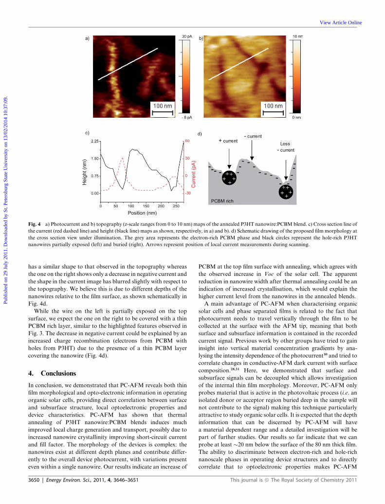
Fig. 4 a) Photocurrent and b) topography (z-scale ranges from 0 to 10 nm) maps of the annealed P3HT nanowire:PCBM blend. c) Cross section line of
the current (red dashed line) and height (black line) maps as shown, respectively, in a) and b). d) Schematic drawing of the proposed film morphology at
the cross section view under illumination. The grey area represents the electron-rich PCBM phase and black circles represent the hole-rich P3HT
nanowires partially exposed (left) and buried (right). Arrows represent position of local current measurements during scanning.
Publ
ishe
d on
29
July
201
1. D
ownl
oade
d by
St.
Pete
rsbu
rg S
tate
Uni
vers
ity o
n 13
/02/
2014
10:
37:0
9.
View Article Online
has a similar shape to that observed in the topography whereas
the one on the right shows only a decrease in negative current and
the shape in the current image has blurred slightly with respect to
the topography. We believe this is due to different depths of the
nanowires relative to the film surface, as shown schematically in
Fig. 4d.
While the wire on the left is partially exposed on the top
surface, we expect the one on the right to be covered with a thin
PCBM rich layer, similar to the highlighted features observed in
Fig. 3. The decrease in negative current could be explained by an
increased charge recombination (electrons from PCBM with
holes from P3HT) due to the presence of a thin PCBM layer
covering the nanowire (Fig. 4d).
4. Conclusions
In conclusion, we demonstrated that PC-AFM reveals both thin
film morphological and opto-electronic information in operating
organic solar cells, providing direct correlation between surface
and subsurface structure, local optoelectronic properties and
device characteristics. PC-AFM has shown that thermal
annealing of P3HT nanowire:PCBM blends induces much
improved local charge generation and transport, possibly due to
increased nanowire crystallinity improving short-circuit current
and fill factor. The morphology of the devices is complex: the
nanowires exist at different depth planes and contribute differ-
ently to the overall device photocurrent, with variations present
even within a single nanowire. Our results indicate an increase of
3650 | Energy Environ. Sci., 2011, 4, 3646–3651
PCBM at the top film surface with annealing, which agrees with
the observed increase in Voc of the solar cell. The apparent
reduction in nanowire width after thermal annealing could be an
indication of increased crystallisation, which would explain the
higher current level from the nanowires in the annealed blends.
A main advantage of PC-AFM when characterising organic
solar cells and phase separated films is related to the fact that
photocurrent needs to travel vertically through the film to be
collected at the surface with the AFM tip, meaning that both
surface and subsurface information is contained in the recorded
current signal. Previous work by other groups have tried to gain
insight into vertical material concentration gradients by ana-
lysing the intensity dependence of the photocurrent30 and tried to
correlate changes in conductive-AFM dark current with surface
composition.28,31 Here, we demonstrated that surface and
subsurface signals can be decoupled which allows investigation
of the internal thin film morphology. Moreover, PC-AFM only
probes material that is active in the photovoltaic process (i.e. an
isolated donor or acceptor region buried deep in the sample will
not contribute to the signal) making this technique particularly
attractive to study organic solar cells. It is expected that the depth
information that can be discerned by PC-AFM will have
a material dependent range and a detailed investigation will be
part of further studies. Our results so far indicate that we can
probe at least �20 nm below the surface of the 80 nm thick film.
The ability to discriminate between electron-rich and hole-rich
nanoscale phases in operating device structures and to directly
correlate that to optoelectronic properties makes PC-AFM
This journal is ª The Royal Society of Chemistry 2011

Publ
ishe
d on
29
July
201
1. D
ownl
oade
d by
St.
Pete
rsbu
rg S
tate
Uni
vers
ity o
n 13
/02/
2014
10:
37:0
9.
View Article Online
a valuable tool for the intelligent design of thin film devices based
on nanoscale structures.
Acknowledgements
The authors thank Andy Wain (NPL), Joanna Lee (NPL) and
Roland Hany (EMPA, Switzerland) for discussions. The work
was supported by the EPSRC-NPL Post-Doctoral Research
Partnership (EP/G062056/1) and the SUPERGEN Excitonic
Solar Cell Consortium Grant (EP/G031088/1).
References
1 See 2010 press releases from Heliatek www.heliatek.com (8.3%),Konarka www.konarka.com (8.3%) and Solarmer www.solarmer.com (8.1%).
2 P. G. Nicholson and F. A. Castro, Nanotechnology, 2010, 21, 492001.3 B. Kippelen and J. L. Br�edas, Energy Environ. Sci., 2009, 2, 251.4 D. H. Wang, J. K. Kim, O. O. Park and J. H. Park, Energy Environ.Sci., 2011, 4, 1434.
5 S. D. Oosterhout, M. M. Wienk, S. S. van Bavel, R. Thiedmann,L. J. A. Koster, J. Gilot, J. Loos, V. Schmidt and R. A. J. Janssen,Nat. Mater., 2009, 8, 818.
6 J. S. Moon, J. K. Lee, S. Cho, J. Byun and A. J. Heeger, Nano Lett.,2009, 9, 230.
7 C. M. Bjorstrom, S. Nilsson, A. Bernasik, A. Budkowski,M. Andersson, K. O. Magnusson and E. Moons, Appl. Surf. Sci.,2007, 253, 3906.
8 B. Xue, B. Vaughan, C.-H. Poh, K. B. Burke, L. Thomsen,A. Stapleton, X. Zhou, G. W. Bryant, W. Belcher andP. C. Dastoor, J. Phys. Chem. C, 2010, 114, 15797.
9 W. C. Tsoi, S. J. Spencer, L. Yang, A. M. Ballantyne,P. G. Nicholson, A. Turnbull, A. G. Shard, C. E. Murphy,D. D. C. Bradley, J. Nelson and J. S. Kim, Macromolecules, 2011,44, 2944.
10 D. Chen, A. Nakahara, D. G. Wei, D. Nordlund and T. P. Russell,Nano Lett., 2011, 11, 561.
11 C. C. Lin, Y. Y. Lin, S. S. Li, C. C. Yu, C. L. Huang, S. H. Lee,C. H. Du, J. J. Lee, H. L. Chen and C. W. Chen, Energy Environ.Sci., 2011, 4, 1434.
This journal is ª The Royal Society of Chemistry 2011
12 O. Douheret, A. Swinnen, S. Bertho, I. Haeldermans, J. D’Haen,M. D’Olieslaeger, D. Vanderzande and J. V. Manca, Progr.Photovolt.: Res. Appl., 2007, 15, 713.
13 H. Sakaguchi, F. Iwata, A. Hirai, A. Sasaki and T. Nagamura, Jpn. J.Appl. Phys., 1999, 38, 3908.
14 D. C. Coffey, O. G. Reid, D. B. Rodovsky, G. P. Bartholomew andD. S. Ginger, Nano Lett., 2007, 7, 738.
15 L. S. C. Pingree, O. G. Reid and D. S. Ginger, Nano Lett., 2009, 9,2946.
16 H. Xin, O. G. Reid, G. Ren, F. S. Kim, D. S. Ginger andS. A. Jenekhe, ACS Nano, 2010, 4, 1861.
17 X. D. Dang, A. B. Tamayo, J. Seo, C. V. Hoven, B. Walker andT. Q. Nguyen, Adv. Funct. Mater., 2010, 20, 3314.
18 X. D. Dang, A. Mikhailovsky and T. Q. Nguyen, Appl. Phys. Lett.,2010, 97, 113303.
19 B. H. Hamadani, S. Jung, P. M. Haney, L. J. Richter andN. B. Zhitenev, Nano Lett., 2010, 10, 1611.
20 F. S. Kim, G. Q. Ren and S. A. Jenekhe, Chem. Mater., 2011, 23, 682.21 L. Qiu, W. H. Lee, X. Wang, J. S. Kim, J. A. Lim, D. Kwak, S. Lee
and K. Cho, Adv. Mater., 2009, 21, 1349.22 J. S. Kim, J. H. Lee, J. H. Park, C. Shim, M. Sim and K. Cho, Adv.
Funct. Mater., 2011, 21, 480.23 Y. Kim, S. A. Choulis, J. Nelson, D. D. C. Bradley, S. Cook and
J. R. Durant, Appl. Phys. Lett., 2005, 86, 1371.24 M. Campoy-Quiles, T. Ferenczi, T. Agostinelli, P. G. Etchegoin,
Y. Kim, T. D. Anthopoulos, P. N. Stavrinou, D. D. C. Bradley andJ. Nelson, Nat. Mater., 2008, 7, 158.
25 X. Yang, J. Loos, S. C. Veenstra, W. J. H. Verhees, M. M. Wienk,J. M. Kroon, M. A. J. Michaels and R. A. J. Janseen, Nano Lett.,2005, 5, 579.
26 F. A. de Castro, J. Heier, F. Nuesch and R. Hany, IEEE J. Sel. Top.Quantum Electron., 2010, 16, 1690.
27 J. H. Kim, J. H. Park, J. H. Lee, J. S. Kim, M. Sim, C. Shim andK. Cho, J. Mater. Chem., 2010, 20, 7398.
28 A. H. Rice, R. Giridharagopal, S. X. Zheng, F. S. Ohuchi,D. S. Ginger and C. K. Luscombe, ACS Nano, 2011, 5,3132.
29 H. J. Snaith, N. C. Greenham and R. H. Friend, Adv. Mater., 2004,16, 1640.
30 O. G. Reid, H. Xin, S. A. Jenekhe and D. S. Ginger, J. Appl. Phys.,2010, 108, 084320.
31 M. Dante, J. Peet and T. Q. Nguyen, J. Phys. Chem. C, 2008, 112,7241.
Energy Environ. Sci., 2011, 4, 3646–3651 | 3651