Embed Size (px)
Citation preview
Phys. Status Solidi A, 1–6 (2010) / DOI 10.1002/pssa.200983706 p s sa
statu
s
soli
di
www.pss-a.comph
ysi
ca
applications and materials science
Ultraviolet photoconductive sensorbased on single ZnO nanowire
O. Lupan*,1,2, G. Chai3, L. Chow**,1,4, G. A. Emelchenko5, H. Heinrich1,4, V. V. Ursaki6,7, A. N. Gruzintsev8,I. M. Tiginyanu7,9, and A. N. Redkin8
1 Department of Physics, University of Central Florida, PO Box 162385, Orlando, FL 32816, USA2 Department of Microelectronics and Semiconductor Devices, Technical University of Moldova, Stefan cel Mare Blvd. 168,
2004 Chisinau, Republic of Moldova3 Apollo Technologies, Inc. 205 Waymont Court, S111, Lake Mary, FL 32746, USA4 Advanced Materials Processing and Analysis Center, and Department of Mechanical, Materials, and Aerospace Engineering,
University of Central Florida, PO Box 162385, Orlando, FL 32816, USA5 Institute of Solid State Physics, Russian Academy of Science, 142432 Chernogolovka, Moscow District, Russia6 Institute of Applied Physics of the Academy of Sciences of Moldova, 2028 Chisinau, Republic of Moldova7 National Center for Materials Study and Testing, Technical University of Moldova, 2004 Chisinau, Republic of Moldova8 Institute of Microelectronics Technology and High Purity Materials, Russian Academy of Sciences, 142432 Chernogolovka,
Moscow District, Russia9 Laboratory of Nanotechnology, Institute of Electronic Engineering and Industrial Technologies, Academy of Sciences of Moldova,
2028 Chisinau, Republic of Moldova
Received 30 May 2009, revised 24 October 2009, accepted 15 January 2010
Published online 28 May 2010
Keywords CVD, nanodevices, nanowires, photoconduction, structure, ZnO
* Corresponding author: e-mail [email protected], [email protected], Phone: þ1 407 823 5117, Fax: þ1 407 823 5112** e-mail [email protected], Phone: þ1 407 823 2333, Fax: þ1 407 823 5112
ZnO nanowires were synthesized by the CVD procedure and
have been investigated by SEM, TEM, SAED, Raman, and cw
PL spectroscopy. The fabrication of an ultraviolet (UV)
photoconductive detector based on single ZnO nanowire
(100 nm in diameter) is presented. This nanostructure detector
is prepared in an Focused Ion Beam (FIB) set-up by using
nanodeposition for metal electrodes. The photoresponse of the
UV sensor are studied using a UV source with an incident peak
wavelength of 365 nm. It was demonstrated that the output
signal of the sensors is reproducible under UV irradiation. The
photoresponse and characteristics of the ZnO nanowire-device
demonstrates that focused ion beam process offers a way to
fabricate novel nanodevices on a single ZnO nanowire with
diameters as small as 100 nm. The presented single ZnO
nanowire sensor proves to be promising for application in
various processes.
� 2010 WILEY-VCH Verlag GmbH & Co. KGaA, Weinheim
1 Introduction Recently, wide-gap semiconductingoxide micro- and nanostructures based on ZnO, SnO2, TiO2
have attracted tremendous research interest due to theirultraviolet (UV) photoresponse and their optical transpar-ency in the visible spectral range [1–9]. In particular, quasi-one-dimensional (Q1D) ZnO nanowires/nanorods are prom-ising as a new type of low-cost and high-speed UV nanoscalephotoconductive detectors and optical switches [1, 2, 6, 7, 9].The low dimensions of such nanostructures promise increasein electronic device packing density, low power consumption,and also enhanced UV sensing properties. Q1D nanostructureswith small diameters (<100 nm) exhibit a large surface-to-
volume ratio which makes them highly susceptible to alteredelectrical properties by means of electron–hole generation orrecombination during UV exposure.
UV detection with nanowires is normally realized bymonitoring the current–voltage or the electrical conductancevariation when exposed to UV radiation. Due to the uniquegeometry of nanowires the active volume contributing todark current (as a source of noise) is one thousandth of anormal size detector. This allows one to reach a highersensitivity by using a single nanowire in devices.
In particular, Yang and co-workers [1] used electron-beam lithography to fabricate nanowire-based UV
� 2010 WILEY-VCH Verlag GmbH & Co. KGaA, Weinheim
2 O. Lupan et al.: Ultraviolet photoconductive sensor based on single ZnO nanowirep
hys
ica ssp st
atu
s
solid
i a
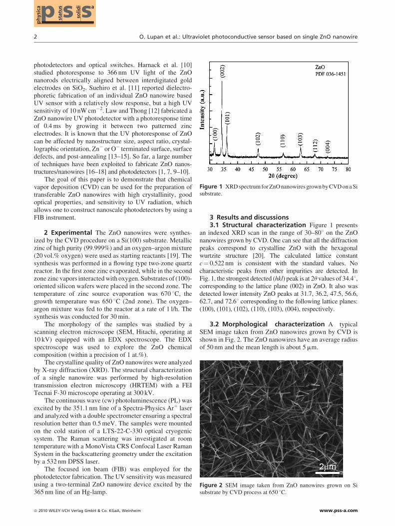
Figure 1 XRD spectrum for ZnO nanowires grown by CVD on a Sisubstrate.
Figure 2 SEM image taken from ZnO nanowires grown on Sisubstrate by CVD process at 650 8C.
photodetectors and optical switches. Harnack et al. [10]studied photoresponse to 366 nm UV light of the ZnOnanorods electrically aligned between interdigitated goldelectrodes on SiO2. Suehiro et al. [11] reported dielectro-phoretic fabrication of an individual ZnO nanowire basedUV sensor with a relatively slow response, but a high UVsensitivity of 10 nW cm�2. Law and Thong [12] fabricated aZnO nanowire UV photodetector with a photoresponse timeof 0.4 ms by growing it between two patterned zincelectrodes. It is known that the UV photoresponse of ZnOcan be affected by nanostructure size, aspect ratio, crystal-lographic orientation, Zn� or O� terminated surface, surfacedefects, and post-annealing [13–15]. So far, a large numberof techniques have been exploited to fabricate ZnO nanos-tructures/nanowires [16–18] and photodetectors [1, 7, 9–10].
The goal of this paper is to demonstrate that chemicalvapor deposition (CVD) can be used for the preparation oftransferable ZnO nanowires with high crystallinity, goodoptical properties, and sensitivity to UV radiation, whichallows one to construct nanoscale photodetectors by using aFIB instrument.
2 Experimental The ZnO nanowires were synthes-ized by the CVD procedure on a Si(100) substrate. Metalliczinc of high purity (99.999%) and an oxygen–argon mixture(20 vol.% oxygen) were used as starting reactants [19]. Thesynthesis was performed in a flowing type two-zone quartzreactor. In the first zone zinc evaporated, while in the secondzone zinc vapors interacted with oxygen. Substrates of (100)-oriented silicon wafers were placed in the second zone. Thetemperature of zinc source evaporation was 670 8C, thegrowth temperature was 650 8C (2nd zone). The oxygen–argon mixture was fed to the reactor at a rate of 1 l/h. Thesynthesis was conducted for 30 min.
The morphology of the samples was studied by ascanning electron microscope (SEM, Hitachi, operating at10 kV) equipped with an EDX spectroscope. The EDXspectroscope was used to explore the ZnO chemicalcomposition (within a precision of 1 at.%).
The crystalline quality of ZnO nanowires were analyzedby X-ray diffraction (XRD). The structural characterizationof a single nanowire was performed by high-resolutiontransmission electron microscopy (HRTEM) with a FEITecnai F-30 microscope operating at 300 kV.
The continuous wave (cw) photoluminescence (PL) wasexcited by the 351.1 nm line of a Spectra-Physics Arþ laserand analyzed with a double spectrometer ensuring a spectralresolution better than 0.5 meV. The samples were mountedon the cold station of a LTS-22-C-330 optical cryogenicsystem. The Raman scattering was investigated at roomtemperature with a MonoVista CRS Confocal Laser RamanSystem in the backscattering geometry under the excitationby a 532 nm DPSS laser.
The focused ion beam (FIB) was employed for thephotodetector fabrication. The UV sensitivity was measuredusing a two-terminal ZnO nanowire device excited by the365 nm line of an Hg-lamp.
� 2010 WILEY-VCH Verlag GmbH & Co. KGaA, Weinheim
3 Results and discussions3.1 Structural characterization Figure 1 presents
an indexed XRD scan in the range of 30–808 on the ZnOnanowires grown by CVD. One can see that all the diffractionpeaks correspond to crystalline ZnO with the hexagonalwurtzite structure [20]. The calculated lattice constantc¼ 0.522 nm is consistent with the standard values. Nocharacteristic peaks from other impurities are detected. InFig. 1, the strongest detected (hkl) peak is at 2u values of 34.48,corresponding to the lattice plane (002) in ZnO. It also wasdetected lower intensity ZnO peaks at 31.7, 36.2, 47.5, 56.6,62.7, and 72.68 corresponding to the following lattice planes:(100), (101), (102), (110), (103), (004), respectively.
3.2 Morphological characterization A typicalSEM image taken from ZnO nanowires grown by CVD isshown in Fig. 2. The ZnO nanowires have an average radiusof 50 nm and the mean length is about 5 mm.
www.pss-a.com
Phys. Status Solidi A (2010) 3
Original
Paper
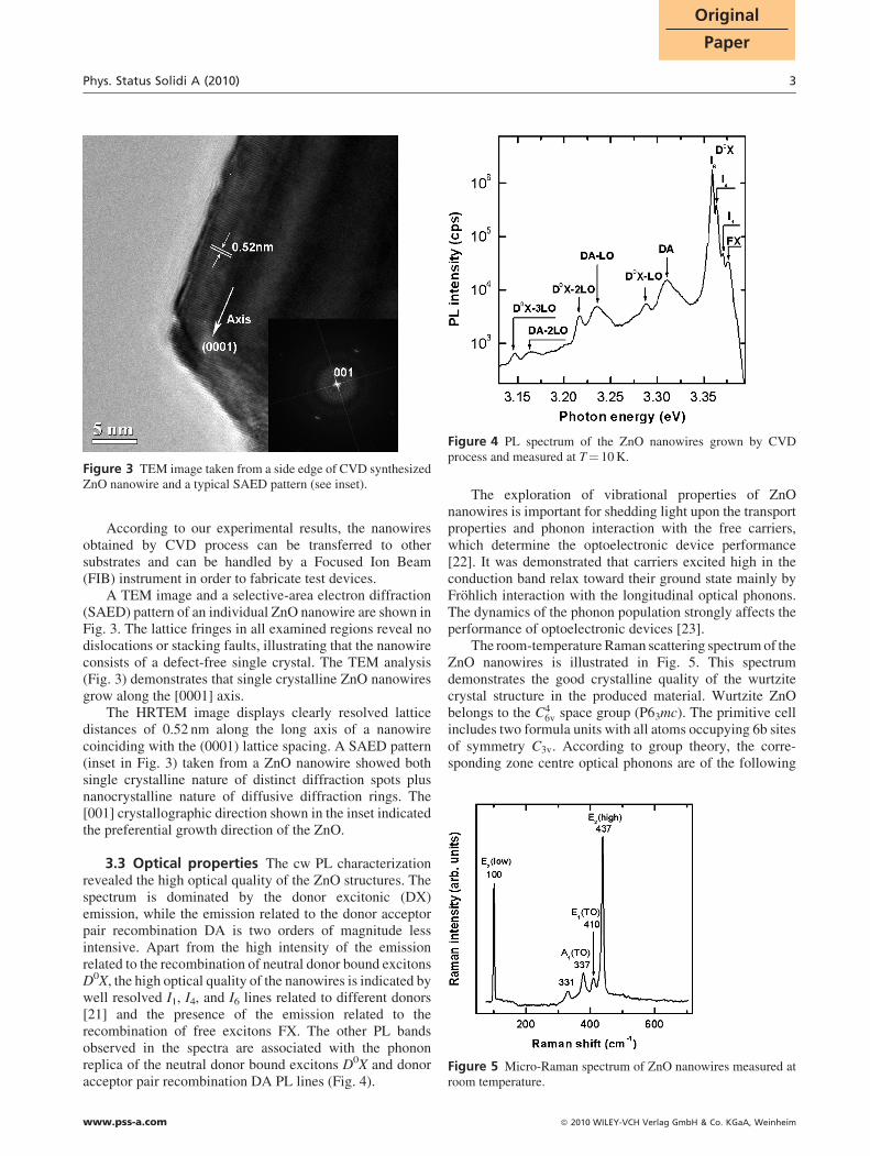
Figure 3 TEM image taken from a side edge of CVD synthesizedZnO nanowire and a typical SAED pattern (see inset).
Figure 4 PL spectrum of the ZnO nanowires grown by CVDprocess and measured at T¼ 10 K.
Figure 5 Micro-Raman spectrum of ZnO nanowires measured atroom temperature.
According to our experimental results, the nanowiresobtained by CVD process can be transferred to othersubstrates and can be handled by a Focused Ion Beam(FIB) instrument in order to fabricate test devices.
A TEM image and a selective-area electron diffraction(SAED) pattern of an individual ZnO nanowire are shown inFig. 3. The lattice fringes in all examined regions reveal nodislocations or stacking faults, illustrating that the nanowireconsists of a defect-free single crystal. The TEM analysis(Fig. 3) demonstrates that single crystalline ZnO nanowiresgrow along the [0001] axis.
The HRTEM image displays clearly resolved latticedistances of 0.52 nm along the long axis of a nanowirecoinciding with the (0001) lattice spacing. A SAED pattern(inset in Fig. 3) taken from a ZnO nanowire showed bothsingle crystalline nature of distinct diffraction spots plusnanocrystalline nature of diffusive diffraction rings. The[001] crystallographic direction shown in the inset indicatedthe preferential growth direction of the ZnO.
3.3 Optical properties The cw PL characterizationrevealed the high optical quality of the ZnO structures. Thespectrum is dominated by the donor excitonic (DX)emission, while the emission related to the donor acceptorpair recombination DA is two orders of magnitude lessintensive. Apart from the high intensity of the emissionrelated to the recombination of neutral donor bound excitonsD0X, the high optical quality of the nanowires is indicated bywell resolved I1, I4, and I6 lines related to different donors[21] and the presence of the emission related to therecombination of free excitons FX. The other PL bandsobserved in the spectra are associated with the phononreplica of the neutral donor bound excitons D0X and donoracceptor pair recombination DA PL lines (Fig. 4).
www.pss-a.com
The exploration of vibrational properties of ZnOnanowires is important for shedding light upon the transportproperties and phonon interaction with the free carriers,which determine the optoelectronic device performance[22]. It was demonstrated that carriers excited high in theconduction band relax toward their ground state mainly byFrohlich interaction with the longitudinal optical phonons.The dynamics of the phonon population strongly affects theperformance of optoelectronic devices [23].
The room-temperature Raman scattering spectrum of theZnO nanowires is illustrated in Fig. 5. This spectrumdemonstrates the good crystalline quality of the wurtzitecrystal structure in the produced material. Wurtzite ZnObelongs to the C4
6v space group (P63mc). The primitive cellincludes two formula units with all atoms occupying 6b sitesof symmetry C3v. According to group theory, the corre-sponding zone centre optical phonons are of the following
� 2010 WILEY-VCH Verlag GmbH & Co. KGaA, Weinheim
4 O. Lupan et al.: Ultraviolet photoconductive sensor based on single ZnO nanowirep
hys
ica ssp st
atu
s
solid
i a
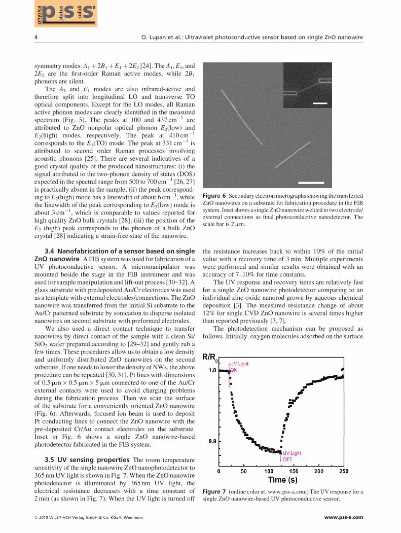
Figure 6 Secondary electron micrographs showing the transferredZnO nanowires on a substrate for fabrication procedure in the FIBsystem. Inset shows a single ZnO nanowire welded to two electrode/external connections as final photoconductive nanodetector. Thescale bar is 2 mm.
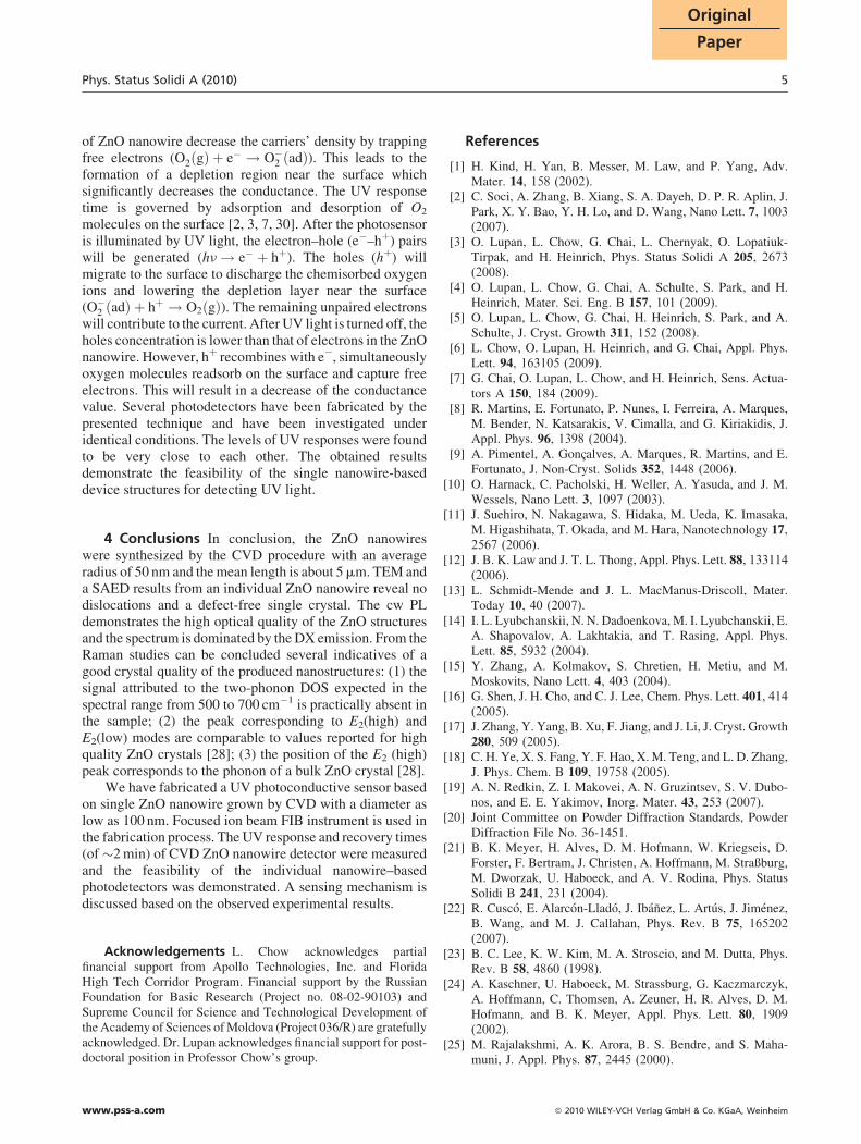
Figure 7 (online color at: www.pss-a.com) The UV response for asingle ZnO nanowire-based UV photoconductive sensor.
symmetry modes: A1þ 2B1þE1þ 2E2 [24]. The A1, E1, and2E2 are the first-order Raman active modes, while 2B1
phonons are silent.The A1 and E1 modes are also infrared-active and
therefore split into longitudinal LO and transverse TOoptical components. Except for the LO modes, all Ramanactive phonon modes are clearly identified in the measuredspectrum (Fig. 5). The peaks at 100 and 437 cm�1 areattributed to ZnO nonpolar optical phonon E2(low) andE2(high) modes, respectively. The peak at 410 cm�1
corresponds to the E1(TO) mode. The peak at 331 cm�1 isattributed to second order Raman processes involvingacoustic phonons [25]. There are several indicatives of agood crystal quality of the produced nanostructures: (i) thesignal attributed to the two-phonon density of states (DOS)expected in the spectral range from 500 to 700 cm�1 [26, 27]is practically absent in the sample; (ii) the peak correspond-ing to E2(high) mode has a linewidth of about 6 cm�1, whilethe linewidth of the peak corresponding to E2(low) mode isabout 3 cm�1, which is comparable to values reported forhigh quality ZnO bulk crystals [28]; (iii) the position of theE2 (high) peak corresponds to the phonon of a bulk ZnOcrystal [28] indicating a strain-free state of the nanowire.
3.4 Nanofabrication of a sensor based on singleZnO nanowire A FIB system was used for fabrication of aUV photoconductive sensor. A micromanipulator wasmounted beside the stage in the FIB instrument and wasused for sample manipulation and lift-out process [30–32]. Aglass substrate with predeposited Au/Cr electrodes was usedas a template with external electrodes/connections. The ZnOnanowire was transferred from the initial Si substrate to theAu/Cr patterned substrate by sonication to disperse isolatednanowires on second substrate with preformed electrodes.
We also used a direct contact technique to transfernanowires by direct contact of the sample with a clean Si/SiO2 wafer prepared according to [29–32] and gently rub afew times. These procedures allow us to obtain a low densityand uniformly distributed ZnO nanowires on the secondsubstrate. If one needs to lower the density of NWs, the aboveprocedure can be repeated [30, 31]. Pt lines with dimensionsof 0.5 mm� 0.5 mm� 5 mm connected to one of the Au/Crexternal contacts were used to avoid charging problemsduring the fabrication process. Then we scan the surfaceof the substrate for a conveniently oriented ZnO nanowire(Fig. 6). Afterwards, focused ion beam is used to depositPt conducting lines to connect the ZnO nanowire with thepre-deposited Cr/Au contact electrodes on the substrate.Inset in Fig. 6 shows a single ZnO nanowire-basedphotodetector fabricated in the FIB system.
3.5 UV sensing properties The room temperaturesensitivity of the single nanowire ZnO nanophotodetector to365 nm UV light is shown in Fig. 7. When the ZnO nanowirephotodetector is illuminated by 365 nm UV light, theelectrical resistance decreases with a time constant of2 min (as shown in Fig. 7). When the UV light is turned off
� 2010 WILEY-VCH Verlag GmbH & Co. KGaA, Weinheim
the resistance increases back to within 10% of the initialvalue with a recovery time of 3 min. Multiple experimentswere performed and similar results were obtained with anaccuracy of 7–10% for time constants.
The UV response and recovery times are relatively fastfor a single ZnO nanowire photodetector comparing to anindividual zinc oxide nanorod grown by aqueous chemicaldeposition [3]. The measured resistance change of about12% for single CVD ZnO nanowire is several times higherthan reported previously [3, 7].
The photodetection mechanism can be proposed asfollows. Initially, oxygen molecules adsorbed on the surface
www.pss-a.com
Phys. Status Solidi A (2010) 5
Original
Paper
of ZnO nanowire decrease the carriers’ density by trappingfree electrons (O2ðgÞ þ e� ! O�2 ðadÞ). This leads to theformation of a depletion region near the surface whichsignificantly decreases the conductance. The UV responsetime is governed by adsorption and desorption of O2
molecules on the surface [2, 3, 7, 30]. After the photosensoris illuminated by UV light, the electron–hole (e�–hþ) pairswill be generated (hn! e� þ hþ). The holes (hþ) willmigrate to the surface to discharge the chemisorbed oxygenions and lowering the depletion layer near the surface(O�2 ðadÞ þ hþ ! O2ðgÞ). The remaining unpaired electronswill contribute to the current. After UV light is turned off, theholes concentration is lower than that of electrons in the ZnOnanowire. However, hþ recombines with e�, simultaneouslyoxygen molecules readsorb on the surface and capture freeelectrons. This will result in a decrease of the conductancevalue. Several photodetectors have been fabricated by thepresented technique and have been investigated underidentical conditions. The levels of UV responses were foundto be very close to each other. The obtained resultsdemonstrate the feasibility of the single nanowire-baseddevice structures for detecting UV light.
4 Conclusions In conclusion, the ZnO nanowireswere synthesized by the CVD procedure with an averageradius of 50 nm and the mean length is about 5 mm. TEM anda SAED results from an individual ZnO nanowire reveal nodislocations and a defect-free single crystal. The cw PLdemonstrates the high optical quality of the ZnO structuresand the spectrum is dominated by the DX emission. From theRaman studies can be concluded several indicatives of agood crystal quality of the produced nanostructures: (1) thesignal attributed to the two-phonon DOS expected in thespectral range from 500 to 700 cm�1 is practically absent inthe sample; (2) the peak corresponding to E2(high) andE2(low) modes are comparable to values reported for highquality ZnO crystals [28]; (3) the position of the E2 (high)peak corresponds to the phonon of a bulk ZnO crystal [28].
We have fabricated a UV photoconductive sensor basedon single ZnO nanowire grown by CVD with a diameter aslow as 100 nm. Focused ion beam FIB instrument is used inthe fabrication process. The UV response and recovery times(of �2 min) of CVD ZnO nanowire detector were measuredand the feasibility of the individual nanowire–basedphotodetectors was demonstrated. A sensing mechanism isdiscussed based on the observed experimental results.
Acknowledgements L. Chow acknowledges partialfinancial support from Apollo Technologies, Inc. and FloridaHigh Tech Corridor Program. Financial support by the RussianFoundation for Basic Research (Project no. 08-02-90103) andSupreme Council for Science and Technological Development ofthe Academy of Sciences of Moldova (Project 036/R) are gratefullyacknowledged. Dr. Lupan acknowledges financial support for post-doctoral position in Professor Chow’s group.
www.pss-a.com
References
[1] H. Kind, H. Yan, B. Messer, M. Law, and P. Yang, Adv.Mater. 14, 158 (2002).
[2] C. Soci, A. Zhang, B. Xiang, S. A. Dayeh, D. P. R. Aplin, J.Park, X. Y. Bao, Y. H. Lo, and D. Wang, Nano Lett. 7, 1003(2007).
[3] O. Lupan, L. Chow, G. Chai, L. Chernyak, O. Lopatiuk-Tirpak, and H. Heinrich, Phys. Status Solidi A 205, 2673(2008).
[4] O. Lupan, L. Chow, G. Chai, A. Schulte, S. Park, and H.Heinrich, Mater. Sci. Eng. B 157, 101 (2009).
[5] O. Lupan, L. Chow, G. Chai, H. Heinrich, S. Park, and A.Schulte, J. Cryst. Growth 311, 152 (2008).
[6] L. Chow, O. Lupan, H. Heinrich, and G. Chai, Appl. Phys.Lett. 94, 163105 (2009).
[7] G. Chai, O. Lupan, L. Chow, and H. Heinrich, Sens. Actua-tors A 150, 184 (2009).
[8] R. Martins, E. Fortunato, P. Nunes, I. Ferreira, A. Marques,M. Bender, N. Katsarakis, V. Cimalla, and G. Kiriakidis, J.Appl. Phys. 96, 1398 (2004).
[9] A. Pimentel, A. Goncalves, A. Marques, R. Martins, and E.Fortunato, J. Non-Cryst. Solids 352, 1448 (2006).
[10] O. Harnack, C. Pacholski, H. Weller, A. Yasuda, and J. M.Wessels, Nano Lett. 3, 1097 (2003).
[11] J. Suehiro, N. Nakagawa, S. Hidaka, M. Ueda, K. Imasaka,M. Higashihata, T. Okada, and M. Hara, Nanotechnology 17,2567 (2006).
[12] J. B. K. Law and J. T. L. Thong, Appl. Phys. Lett. 88, 133114(2006).
[13] L. Schmidt-Mende and J. L. MacManus-Driscoll, Mater.Today 10, 40 (2007).
[14] I. L. Lyubchanskii, N. N. Dadoenkova, M. I. Lyubchanskii, E.A. Shapovalov, A. Lakhtakia, and T. Rasing, Appl. Phys.Lett. 85, 5932 (2004).
[15] Y. Zhang, A. Kolmakov, S. Chretien, H. Metiu, and M.Moskovits, Nano Lett. 4, 403 (2004).
[16] G. Shen, J. H. Cho, and C. J. Lee, Chem. Phys. Lett. 401, 414(2005).
[17] J. Zhang, Y. Yang, B. Xu, F. Jiang, and J. Li, J. Cryst. Growth280, 509 (2005).
[18] C. H. Ye, X. S. Fang, Y. F. Hao, X. M. Teng, and L. D. Zhang,J. Phys. Chem. B 109, 19758 (2005).
[19] A. N. Redkin, Z. I. Makovei, A. N. Gruzintsev, S. V. Dubo-nos, and E. E. Yakimov, Inorg. Mater. 43, 253 (2007).
[20] Joint Committee on Powder Diffraction Standards, PowderDiffraction File No. 36-1451.
[21] B. K. Meyer, H. Alves, D. M. Hofmann, W. Kriegseis, D.Forster, F. Bertram, J. Christen, A. Hoffmann, M. Straßburg,M. Dworzak, U. Haboeck, and A. V. Rodina, Phys. StatusSolidi B 241, 231 (2004).
[22] R. Cusco, E. Alarcon-Llado, J. Ibanez, L. Artus, J. Jimenez,B. Wang, and M. J. Callahan, Phys. Rev. B 75, 165202(2007).
[23] B. C. Lee, K. W. Kim, M. A. Stroscio, and M. Dutta, Phys.Rev. B 58, 4860 (1998).
[24] A. Kaschner, U. Haboeck, M. Strassburg, G. Kaczmarczyk,A. Hoffmann, C. Thomsen, A. Zeuner, H. R. Alves, D. M.Hofmann, and B. K. Meyer, Appl. Phys. Lett. 80, 1909(2002).
[25] M. Rajalakshmi, A. K. Arora, B. S. Bendre, and S. Maha-muni, J. Appl. Phys. 87, 2445 (2000).
� 2010 WILEY-VCH Verlag GmbH & Co. KGaA, Weinheim
6 O. Lupan et al.: Ultraviolet photoconductive sensor based on single ZnO nanowirep
hys
ica ssp st
atu
s
solid
i a
[26] F. Reuss, C. Kichner, Th. Gruber, R. Kling, S. Maschek, W.Limmer, A. Waag, and P. Ziemann, J. Appl. Phys. 95, 3385(2004).
[27] J. Serrano, A. H. Romero, F. J. Manjon, R. Lauck, M.Cardona, and A. Rubio, Phys. Rev. B 69, 094306(2004).
[28] J. Serrano, F. J. Manjon, A. H. Romero, F. Widulle,R. Lauck, and M. Cardona, Phys. Rev. Lett. 90, 055510(2003).
[29] S. T. Shishiyanu, O. I. Lupan, T. S. Shishiyanu, V. P. Sontea,and S. K. Railean, Electrochim. Acta 49, 4433 (2004).
� 2010 WILEY-VCH Verlag GmbH & Co. KGaA, Weinheim
[30] O. Lupan, L. Chow, and G. Chai, Sens. Actuators B 141, 511(2009).
[31] O. Lupan, V. V. Ursaki, G. Chai, L. Chow, G. A. Emel-chenko, I. M. Tiginyanu, A. N. Gruzintsev, and A. N. Redkin,Sens. Actuators B 144, 56 (2010).
[32] G. Chai, O. Lupan, and L. Chow, Focused ion beam fabrica-tion of carbon nanotube and ZnO nanodevices, in: P. Russell,I. Utke, S. Moshkalev (eds.), Nanofabrication Using FocusedIon and Electron Beams: Principles and Applications, Nano-fabrication with FEB and FIB (Oxford University Press,2010), pp. 1–10.
www.pss-a.com
![Enhanced Performance of a ZnO Nanowire-Based Self-Powered ... · tric NW-based Schottky-contact sensors such as strain sensor, [11 ] protein sensor, [8] pH sensor, 9 ] and photodetector](https://img.pdfslide.us/doc/110x75/5fa7e9ea1e06e553a139b212/enhanced-performance-of-a-zno-nanowire-based-self-powered-tric-nw-based-schottky-contact.jpg)