Embed Size (px)
Citation preview

ASD0016561 Rev. C Information furnished by Analog Devices is believed to be accurate and reliable. However, no responsibility is assumed by Analog Devices for its use, nor for any infringements of patents or other rights of third parties that may result from its use. Specifications subject to change without notice. No license is granted by implication or otherwise under any patent or patent rights of Analog Devices. Trademarks and registered trademarks are the property of their respective companies.
1.0 Scope
This specification documents the detail requirements for space qualified product manufactured on Analog Devices, Inc.'s QML certified line per MIL-PRF-38535 Level V except as modified herein.
The manufacturing flow described in the STANDARD SPACE LEVEL PRODUCTS PROGRAM brochure is to be considered a part of this specification. http://www.analog.com/aeroinfo
This data specifically details the space grade version of this product. A more detailed operational description and a complete data sheet for commercial product grades can be found at http://www.analog.com/ADuM3190
2.0 Part Number
The complete part number(s) of this specification follows:
Specific Part Number Description
ADUM3190P703F High Stability Isolated Error Amplifier
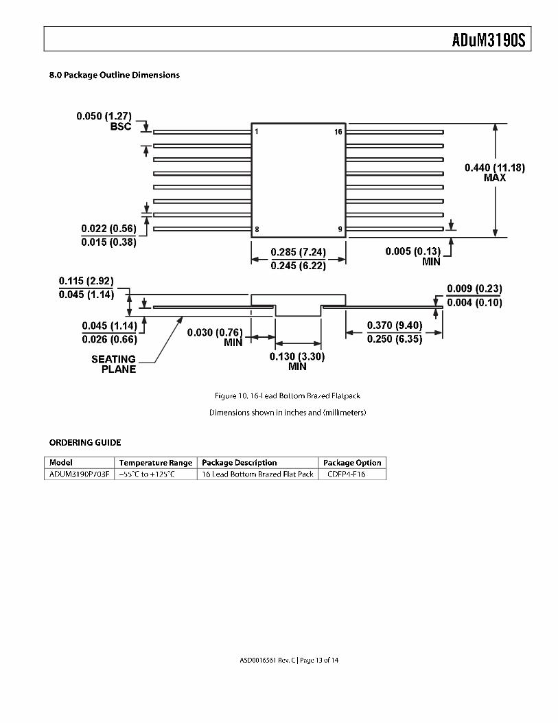
3.0 Case Outline
The case outline(s) are as designated in MIL-STD-1835 and as follows:
Outline Letter Descriptive Designator Terminals Lead Finish Package style
X CDFP4-F16 16 lead Hot Solder Dip Bottom Brazed FlatPack

Supply Voltage for Side 1 (3.0 V to 20 V). 1/
Ground Reference for Side 1. 3/, 12/
Internal Supply Voltage for Side 1. 2/
Reference Output Voltage for Side 1. 5/
Ground 6/, 12/
Isolated Output Voltage 2, Open-Drain Output. 7/
Isolated Output Voltage.
Ground Reference for Side 1. 3/, 12/
Ground Reference for Side 2. 4/
Output of the Op Amp. 8/
Inverting Op Amp Input. 9/
Noninverting Op Amp Input. 10/
Reference Output Voltage for Side 2. 11/
Internal Supply Voltage for Side 2. 2/
Ground Reference for Side 2. 4/
Supply Voltage for Side 2 (3.0 V to 20) V 1/
Metal Lid electrically connected to ground (GND1)
1/ Connect a ceramic bypass capacitor of value 1 μF between VDD1 (Pin 1) and GND1 (Pin 2) and between VDD2 (Pin 16) and GND2 (Pin 15) 2/ Connect a 1 μF capacitor between VREG1 (Pin 3) and GND1 (Pin2) and VREG2 (Pin 14)and GND2(Pin 15). 3/ Pin 2 and Pin 8 are internally connected, and connecting both to GND1 is recommended. 4/ Pin 9 and Pin 15 are internally connected, and connecting both to GND2 is recommended. 5/ The maximum capacitance for this pin (CREFOUT1) must not exceed 15 pF. 6/ Connect Pin 5 to GND1; do not leave this pin floating. 7/ Connect a pull-up resistor between EAOUT2 and VDD1 for current up to 1 mA. 8/ A loop compensation network can be connected between the COMP pin and the −IN pin. 9/ Pin 11 is the connection for the power supply setpoint and compensation network. 10/ Pin 12 can be used as a reference input. 11/ The maximum capacitance for this pin (CREFOUT) must not exceed 15 pF. 12/ Internally connected to Metal Lid.

4.0 Specifications
4.1. Absolute Maximum Ratings 1/
Supply voltage (VDD1, VDD2) ........................................................... 24 V 2/
Supply voltage (VREG1, VREG2) ........................................................ 3.6 V 2/
Input voltage (+IN, -IN) .................................................................. 3.6 V 8/
Output voltages ( )...................................... 3.6 V
Output voltages ( )................................................................... 5.8 V
Output Current per Output Pin....................................................... -11 mA to +11 mA 8/
Common-Mode Transients ............................................................ -100kV/µs – 100kV/µs 3/
Storage temperature range ........................................................... -65C to +150C
Junction temperature maximum (TJ) ............................................ +150C
Lead temperature (soldering, 60 seconds) .................................. +300C
Thermal resistance, junction-to-case (JC) ................................... 60 C/W 4/
Thermal resistance, junction-to-ambient (JA) .............................. 98 C/W 4/
ESD Sensitivity (HBM)……………………………………………….. Class 2
4.2. Recommended Operating Conditions
Supply voltage (VDD1, VDD2) ........................................................... 3.0 V to 20.0 V
Ambient operating temperature range (TA)…………………………. -55C to +125C
Max input signal rise and fall times (tR, tF) ....................................... 1ms
4.3. Nominal Operating Performance Characteristics 5/
Input Capacitance ...................................................................... 2 pF
EAOUT Impedance ( ............................. High-Z Input-to-Output Capacitance (CI-O) .............................................. 2.2pF 7/
Input Capacitance (CI)................................................................. 4pF
Maximum Working Insulation Voltage ..........................................100Vpeak 9/
4.4. Radiation Features
Maximum total dose available (dose rate = 50 – 300 rads(Si)/s)….30 k rads(Si)
1/ Stresses above those listed under Absolute Maximum Ratings may cause permanent damage to the device. This is a stress rating only; functional operation of the device at these or any other conditions outside of those indicated in the operation sections of this specification is not implied. Exposure to absolute maximum ratings for extended periods may affect device reliability. 2/ All voltages are relative to their respective grounds. 3/ Refers to common-mode transients across the insulation barrier. Common-mode transients exceeding the absolute maximum ratings may cause latch-up or permanent damage 4/ Measurement taken under absolute worst case condition and represents data taken with thermal camera for highest power density location. See MIL-STD-1835 for average ΘJC number.
5/ All typical specifications are at TA = 25°C and VDD1 = VDD2 = 5 V, unless otherwise noted.
6/ The device is considered a 2-terminal device; Pin 1 through Pin 8 are shorted together, and Pin 9 through Pin 16 are shorted together
7/ Input capacitance is from any input data pin to ground.
8/ See Figure 2 for maximum rated power for various temperatures.
9/ Maximum voltage magnitude imposed across the isolation barrier. Long term operation at this high voltage can lead to shortened isolation life. Continuous working voltage exceeding the rated value may cause permanent damage.
10/ Accelerated life testing using voltage levels higher than the rated continuous working voltage is on going for this part. Expected completion is end of 2018.


TABLE IA NOTES:
1/ TA nom = 25ºC, TA max = 125ºC, TA min = -55ºC and VDD1 = VDD2 = 3V min, VDD1 = VDD2 = 5V nom and VDD1 = VDD2 = 20V max unless otherwise
noted.
2/ Parameter is part of device initial characterization which is only repeated after design and process changes or with subsequent wafer lots.
3/ Parameter is not tested post irradiation
4/ Output gain is defined as the slope of the best-fit line of the output voltage vs. the input voltage over the specified input range, with the offset error adjusted out
5/ Output linearity is defined as the peak-to-peak output deviation from the best-fit line of the output gain, expressed as a percentage of the full-scale output voltage.
For VDD2, if ramping the supply voltage to turn on the outputs, be sure to start ramp where 2.55V < VDD2 < 2.7V.

7/ Accuracy is measured using circuit configuration in Figure 3 for EAout and Figure 4 for EAout2
TABLE IB NOTES:
1/ Parameter is part of device initial characterization which is only repeated after design and process changes or with subsequent wafer lots TA = 25ºC.
2/ Parameter is not tested post irradiation
3/ The device is considered a 2-terminal device: Pin 1 through Pin 8 are shorted together and Pin 9 through Pin 16 are shorted together.

Table IIA Notes: 1/ PDA applies to Table I subgroup 1 and Table IIB delta parameters. 2/ See Table IIB for delta parameters 3/ Parameters noted in Table IA are not tested post irradiation.
1/ 240 hour burn in and group C end point electrical parameters. 2/ Deltas are performed at room temperature TA = +25°C.
5.0 Burn-In Life Test, and Radiation
5.1. Burn-In Test Circuit, Life Test Circuit
5.1.1. The test conditions and circuit shall be maintained by the manufacturer under document revision level control and shall be made available to the preparing or acquiring activity upon request. The test circuit shall specify the inputs, outputs, biases, and power dissipation, as applicable, in accordance with the intent specified in method 1015 test condition B of MIL –STD-883.
5.1.2. HTRB is not applicable for this drawing.
5.2. Radiation Exposure Circuit
5.2.1. The radiation exposure circuit shall be maintained by the manufacturer under document revision level

control and shall be made available to the preparing and acquiring activity upon request. Total dose irradiation testing shall be performed in accordance with MIL-STD-883 method 1019, condition A.
6.0 MIL-PRF-38535 QMLV Exceptions
6.1. Wafer Fabrication
Wafer fabrication occurs at MIL-PRF-38535 QML Class Q certified facility.
6.2. Wafer Lot Acceptance (WLA)
WLA per MIL-STD-883 TM 5007 is not available for this product. SEM inspection per MIL-STD-883 TM2018 is not applicable to the ADuM3190S. The wafer fabrication process is manufactured using planarized metallization
6.3. Device contains bi-metallic wire bonds (Gold bond wires on Aluminum die pads).
7.0 Application Notes
TEST CIRCUITS

THEORY OF OPERATION
In the test circuits of the ADuM3190 (see Figure 3 through Figure 5), external supply voltages from 3 V to 20 V are provided to the VDD1 and VDD2 pins, and internal regulators provide 3.0 V to operate the internal circuits of each side of the ADuM3190. An internal precision 1.225 V reference provides the reference for the ±1% accuracy of the isolated error amplifier. UVLO circuits monitor the VDDx supplies to turn on the internal circuits when the 2.96 V rising threshold is met and to turn off the error amplifier outputs to a high impedance state when VDDx falls below 2.5 V. The op amp on the right side of the device has a noninverting +IN pin and an inverting −IN pin available for connecting a feedback voltage in an isolated dc-to-dc converter output, usually through a voltage divider. The COMP pin is the op amp output, which can be used to attach resistor and capacitor components in a compensation network. The COMP pin internally drives the Tx transmitter block, which converts the op amp output voltage into an encoded output that is used to drive the digital isolator transformer. On the left side of the ADuM3190, the transformer output PWM signal is decoded by the Rx block, which converts the signal into a voltage that drives an amplifier block; the amplifier block produces the error amplifier output available at the EAOUT pin. The EAOUT pin can deliver ±3 mA and has a voltage level between 0.4 V and 2.4 V, which is typically used to drive the input of a PWM controller in a dc-to-dc circuit. For applications that need more output voltage to drive their controllers, Figure 4 illustrates the use of the EAOUT2 pin output, which delivers up to ±1 mA with an output voltage of 0.6 V to 4.8 V for an output that has a pull-up resistor to a 5 V supply. If the EAOUT2 pull-up resistor connects to a 10 V to 20 V supply, the output is specified to a minimum of 5.0 V to allow use with a PWM controller requiring a minimum input operation of 5V. ACCURACY CIRCUIT OPERATION See Figure 3 and Figure 4 for stability of the accuracy circuits. The op amp on the right side of the ADuM3190, from the −IN pin to the COMP pin, has a unity-gain bandwidth (UGBW) of10 MHz. Figure 6, Bode Plot 1, shows a dashed line for the op amp alone and its 10 MHz pole. Figure 6 also shows the linear isolator alone (the blocks from the op amp output to the ADuM3190 output, labeled as the linear isolator), which introduces a pole at approximately 400 kHz. This total Bode plot of the op amp and linear isolator shows that the phase shift is approximately −180° from the −IN pin to the EAOUT pin before the crossover frequency. Because a −180° phase shift can make the system unstable, adding an integrator configuration, as shown in the test circuits in Figure 3 and Figure 4, consisting of a 2.2 nF capacitor and a 680 Ω resistor helps to make the system stable. In Figure 7, Bode Plot 2 with an integrator configuration added, the system crosses over 0 dB at approximately 100 kHz, but the circuit is more stable with a phase shift of approximately −120°, which yields a stable 60° phase margin. This circuit is used for accuracy tests only, not for real-world applications, because it has a 680 Ω resistor across the isolation barrier to close the loop for the error amplifier; this resistor causes leakage current to flow across the isolation barrier. For this test circuit only, GND1 must be connected to GND2 to create a return for the leakage current created by the 680 Ω resistor connection.

ISOLATED AMPLIFIER CIRCUIT OPERATION
Figure 5 shows an isolated amplifier circuit. In this circuit, the input side amplifier is set as a unity-gain buffer so that the EAOUT output follows the +IN input. The EAOUT2 output follows the EAOUT output, but with a voltage gain of 2.6. This circuit has an open-drain output, which must be pulled up to a supply voltage from 3 V to 20 V using a resistor value set for an output current of up to 1 mA. The EAOUT2 output can be used to drive up to 1 mA to the input of a device that requires a minimum input operation of 5 V. The EAOUT2 circuit has an internal diode clamp to protect the internal circuits from voltages greater than 5 V. The gain, offset, and linearity of EAOUT and EAOUT2 are specified in Table 1 using this test circuit. When designing applications for voltage monitoring using an isolated amplifier, review these specifications, noting that the 1% accuracy specifications for the isolated error amplifier do not apply. In addition, the EAOUT circuit in Figure 5 is shown with an optional external RC low-pass filter with a corner frequency of 500 kHz, which can reduce the 3 MHz output noise from the internal voltage to the PWM converter.

DC CORRECTNESS AND MAGNETIC FIELD IMMUNITY Positive and negative logic transitions at the isolator input cause narrow (~1 ns) pulses to be sent to the decoder via the transformer. The decoder is bistable and is, therefore, either set or reset by the pulses, indicating input logic transitions. In the absence of logic transitions of more than 1 μs at the input, a periodic set of refresh pulses indicative of the correct input state are sent to ensure dc correctness at the output. If the decoder receives no internal pulses for more than approximately 3 μs, the input side is assumed to be unpowered or nonfunctional, in which case the isolator output is forced to a default high impedance state by the watchdog timer circuit. In addition, the outputs are in a default high impedance state while the power is increasing before the UVLO threshold is crossed. The ADuM3190 is immune to external magnetic fields. The limitation on the ADuM3190 magnetic field immunity is set by the condition whereby induced voltage in the transformer receiving coil is sufficiently large to either falsely set or reset the decoder. The following analysis defines the conditions under which this can occur. The 3 V operating condition of the ADuM3190 is examined because it represents the most susceptible mode of operation. The pulses at the transformer output have an amplitude that is greater than 1.0 V. The decoder has a sensing threshold at approximately 0.5 V, therefore establishing a 0.5 V margin within which induced voltages are tolerated. The voltage induced across the receiving coil is given by V = (−dβ/dt) ∑π rn
2, n = 1, 2, … , N where: β is the magnetic flux density (gauss). rn is the radius of the nth turn in the receiving coil (cm). N is the number of turns in the receiving coil. Given the geometry of the receiving coil in the ADuM3190 and an imposed requirement that the induced voltage be, at most, 50% of the 0.5 V margin at the decoder, a maximum allowable magnetic field is calculated, as shown in Figure 8.
For example, at a magnetic field frequency of 1 MHz, the maximum allowable magnetic field of 0.02 kgauss induces a voltage of 0.25 V at the receiving coil. This is approximately 50% of the sensing threshold and does not cause a faulty output transition. Similarly, if such an event were to occur during a transmitted pulse (and had the worst-case polarity), the received pulse is reduced from >1.0 V to 0.75 V, still well above the 0.5 V sensing threshold of the decoder.
The preceding magnetic flux density values correspond to specific current magnitudes at given distances away from the ADuM3190 transformers. Figure 9 shows these allowable current magnitudes as a function of

frequency for selected distances. As shown in Figure 9, the ADuM3190 is immune and can be affected only by extremely large currents operating at a high frequency very close to the component. For the 1 MHz example, a 0.7 kA current must be placed 5 mm away from the ADuM3190 to affect the operation of the device.


![Demistyfing equity-focused evaluations [EFE]](https://img.pdfslide.us/doc/110x75/56815a08550346895dc75589/demistyfing-equity-focused-evaluations-efe.jpg)