Embed Size (px)
Citation preview
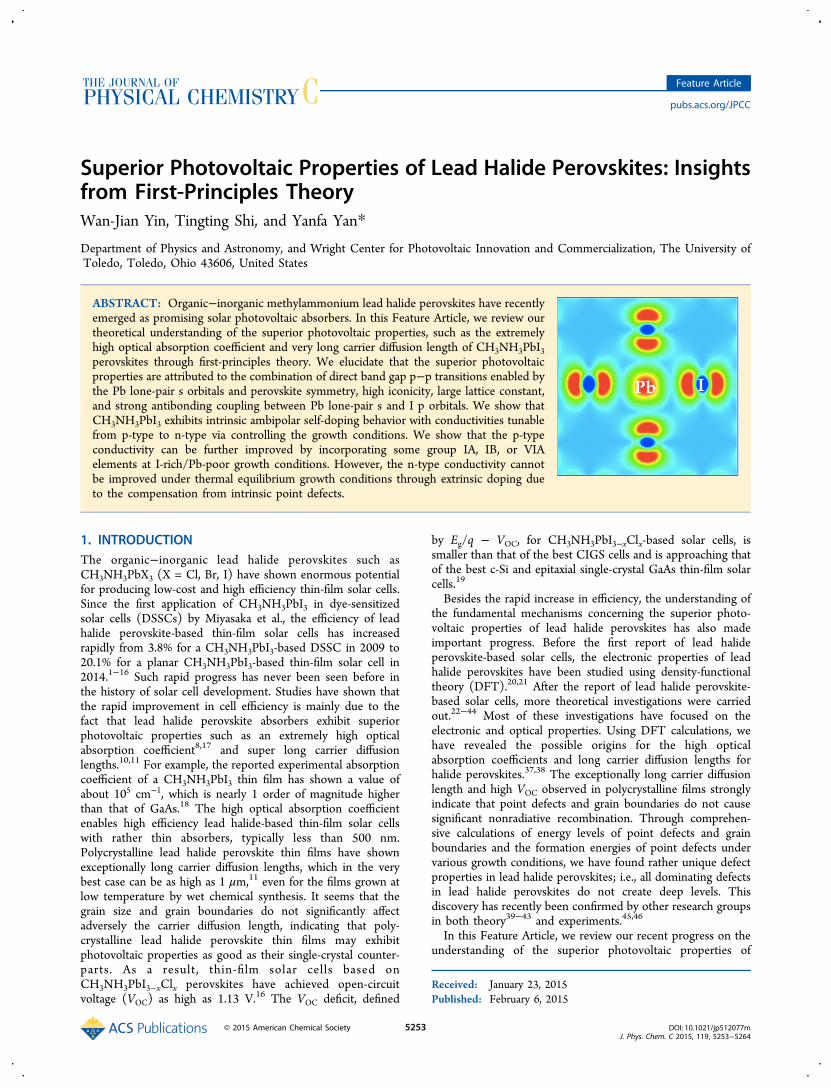
Superior Photovoltaic Properties of Lead Halide Perovskites: Insightsfrom First-Principles TheoryWan-Jian Yin, Tingting Shi, and Yanfa Yan*
Department of Physics and Astronomy, and Wright Center for Photovoltaic Innovation and Commercialization, The University ofToledo, Toledo, Ohio 43606, United States
ABSTRACT: Organic−inorganic methylammonium lead halide perovskites have recentlyemerged as promising solar photovoltaic absorbers. In this Feature Article, we review ourtheoretical understanding of the superior photovoltaic properties, such as the extremelyhigh optical absorption coefficient and very long carrier diffusion length of CH3NH3PbI3perovskites through first-principles theory. We elucidate that the superior photovoltaicproperties are attributed to the combination of direct band gap p−p transitions enabled bythe Pb lone-pair s orbitals and perovskite symmetry, high iconicity, large lattice constant,and strong antibonding coupling between Pb lone-pair s and I p orbitals. We show thatCH3NH3PbI3 exhibits intrinsic ambipolar self-doping behavior with conductivities tunablefrom p-type to n-type via controlling the growth conditions. We show that the p-typeconductivity can be further improved by incorporating some group IA, IB, or VIAelements at I-rich/Pb-poor growth conditions. However, the n-type conductivity cannotbe improved under thermal equilibrium growth conditions through extrinsic doping dueto the compensation from intrinsic point defects.
1. INTRODUCTIONThe organic−inorganic lead halide perovskites such asCH3NH3PbX3 (X = Cl, Br, I) have shown enormous potentialfor producing low-cost and high efficiency thin-film solar cells.Since the first application of CH3NH3PbI3 in dye-sensitizedsolar cells (DSSCs) by Miyasaka et al., the efficiency of leadhalide perovskite-based thin-film solar cells has increasedrapidly from 3.8% for a CH3NH3PbI3-based DSSC in 2009 to20.1% for a planar CH3NH3PbI3-based thin-film solar cell in2014.1−16 Such rapid progress has never been seen before inthe history of solar cell development. Studies have shown thatthe rapid improvement in cell efficiency is mainly due to thefact that lead halide perovskite absorbers exhibit superiorphotovoltaic properties such as an extremely high opticalabsorption coefficient8,17 and super long carrier diffusionlengths.10,11 For example, the reported experimental absorptioncoefficient of a CH3NH3PbI3 thin film has shown a value ofabout 105 cm−1, which is nearly 1 order of magnitude higherthan that of GaAs.18 The high optical absorption coefficientenables high efficiency lead halide-based thin-film solar cellswith rather thin absorbers, typically less than 500 nm.Polycrystalline lead halide perovskite thin films have shownexceptionally long carrier diffusion lengths, which in the verybest case can be as high as 1 μm,11 even for the films grown atlow temperature by wet chemical synthesis. It seems that thegrain size and grain boundaries do not significantly affectadversely the carrier diffusion length, indicating that poly-crystalline lead halide perovskite thin films may exhibitphotovoltaic properties as good as their single-crystal counter-parts. As a result, thin-fi lm solar cells based onCH3NH3PbI3−xClx perovskites have achieved open-circuitvoltage (VOC) as high as 1.13 V.16 The VOC deficit, defined
by Eg/q − VOC, for CH3NH3PbI3−xClx-based solar cells, issmaller than that of the best CIGS cells and is approaching thatof the best c-Si and epitaxial single-crystal GaAs thin-film solarcells.19
Besides the rapid increase in efficiency, the understanding ofthe fundamental mechanisms concerning the superior photo-voltaic properties of lead halide perovskites has also madeimportant progress. Before the first report of lead halideperovskite-based solar cells, the electronic properties of leadhalide perovskites have been studied using density-functionaltheory (DFT).20,21 After the report of lead halide perovskite-based solar cells, more theoretical investigations were carriedout.22−44 Most of these investigations have focused on theelectronic and optical properties. Using DFT calculations, wehave revealed the possible origins for the high opticalabsorption coefficients and long carrier diffusion lengths forhalide perovskites.37,38 The exceptionally long carrier diffusionlength and high VOC observed in polycrystalline films stronglyindicate that point defects and grain boundaries do not causesignificant nonradiative recombination. Through comprehen-sive calculations of energy levels of point defects and grainboundaries and the formation energies of point defects undervarious growth conditions, we have found rather unique defectproperties in lead halide perovskites; i.e., all dominating defectsin lead halide perovskites do not create deep levels. Thisdiscovery has recently been confirmed by other research groupsin both theory39−43 and experiments.45,46
In this Feature Article, we review our recent progress on theunderstanding of the superior photovoltaic properties of
Received: January 23, 2015Published: February 6, 2015
Feature Article
pubs.acs.org/JPCC
© 2015 American Chemical Society 5253 DOI: 10.1021/jp512077mJ. Phys. Chem. C 2015, 119, 5253−5264
CH3NH3PbI3 through DFT calculations. We explain in detailthe roles of the Pb lone-pair s orbitals and the perovskitesymmetry for the exceptionally high optical absorptioncoefficients. We further elucidate the impacts of theantibonding coupling between Pb lone-pair s and I p orbitals,the high ionicity, and the large lattice constant on the defectproperties in CH3NH3PbI3. Moreover, we provide strategies fordoping lead halide perovskite absorbers. We reveal thatimproved p-type conductivity for CH3NH3PbI3 can be realizedby incorporating of group IA, IB, or VIA elements such as Na,K, Rb, Cu, and O at I-rich/Pb-poor growth conditions. Wefurther show that the n-type conductivity of CH3NH3PbI3 ismore difficult to be improved via extrinsic doping due to thecompensation from intrinsic point defects. Our results suggestthat nonequilibrium growth conditions and/or processes maybe required to produce good n-type CH3NH3PbI3 halideperovskites. The understanding of the origins for the superiorphotovoltaic properties and doping properties of lead halideperovskites provides guidance for designing new absorbermaterials or engineering the current perovskite materials foreven more improved device performance.
2. COMPUTATIONAL DETAILS
The calculations reported in this article were carried out byusing the VASP code with the standard frozen-core projectoraugmented-wave (PAW) method.47,48 The cutoff energy for
basis functions was 400 eV. The general gradient approximation(GGA) was used for exchange correlation.49 Atomic positionsare relaxed until all the forces on atoms are below 0.05 eV/Å. Ithas been discussed that it is important to include the effect ofspin−orbital coupling (SOC) in DFT calculations of theelectronic and optical properties of lead halide perovskites dueto the strong relativistic effect of Pb.26−30 However, SOC-GGAsignificantly underestimates the band gap of halide perovskites.For example, the calculated SOC-DFT band gap is about 0.6 eVfor CH3NH3PbI3, much smaller than the experimental gap of1.56 eV. To correct the band gap underestimation, a hybridfunctional such as the Heyd−Scuseria−Ernzerhof (HSE06)functional needs to be used.50 The most advanced calculationapproach is to use SOC-GW calculation.28 However, so far,both SOC-HSE and SOC-GW calculations are very time-consuming and can only be feasible for calculations with smallunit cells. In our study, most calculations require the use oflarge super cells. For these calculations, it is not possible toconsider SOC-HSE or SOC-GW. Fortunately, it is known thatthe errors of using GGA and non-SOC are canceled with eachother in occurrence.25 The defect properties predicted by non-SOC-GGA calculations are confirmed by experiments.46 Ourrecent results show that the calculated optical absorptionspectrum of CH3NH3PbI3 using non-SOC-GGA can matchwell with experimental results measured by spectroscopicellipsometry (unpublished results). Therefore, non-SOC-GGA
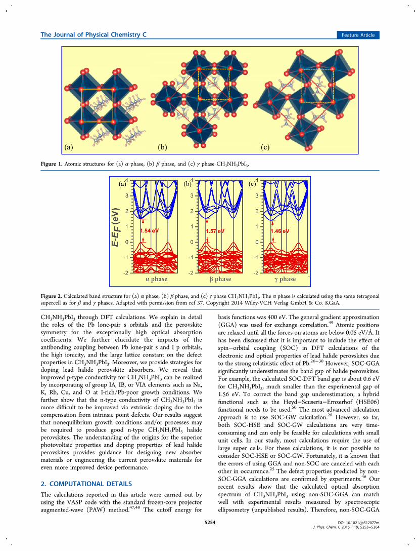
Figure 1. Atomic structures for (a) α phase, (b) β phase, and (c) γ phase CH3NH3PbI3.
Figure 2. Calculated band structure for (a) α phase, (b) β phase, and (c) γ phase CH3NH3PbI3. The α phase is calculated using the same tetragonalsupercell as for β and γ phases. Adapted with permission from ref 37. Copyright 2014 Wiley-VCH Verlag GmbH & Co. KGaA.
The Journal of Physical Chemistry C Feature Article
DOI: 10.1021/jp512077mJ. Phys. Chem. C 2015, 119, 5253−5264
5254
is so far a reasonable and efficient approximation for thecalculation of optical properties and defect physics ofCH3NH3PbI3.At finite temperatures, CH3NH3PbI3 may exhibit three
phases, the cubic (α), tetragonal (β), and orthorhombic (γ)phases, as shown in Figures 1(a), 1(b), and 1(c), respectively.Transitions between those structures at finite temperature oftenhappen in most perovskites.51,52 It was reported that the α to βto γ phase transitions happen at 330 and 160 K, respectively.53
In the α phase, all the octahedra formed by Pb and I atoms areoriented along the same direction. In β and γ phases, some ofthe octahedra rotate to different directions. The large solidboxes and the small dashed boxes in Figures 1(b) and 1(c)indicate the relationship between the unit cells of α, β, and γphases and the unit cells of the α phase. The α phase has aPm3m point symmetry, whereas the point symmetries for β andγ phases are I4/mcm and Pnma-2.The rotation of Pb−I octahedra does not change significantly
the electronic properties of CH3NH3PbI3. Figures 2(a), 2(b),and 2(c) show the calculated band structures for α, β, and γphases, respectively, using DFT with non-SOC-GGA calcu-lations. For better comparison, the band structure of the αphase is calculated with a (√2 × √2 × 2) supercell. The maindifferences between these band structures are the slight splittingof the conduction band minimum (CBM) and valence bandmaximum (VBM) caused by the decreased symmetries. Thissuggests that the Pb−I−Pb bond angle distortions do notchange significantly the electronic structures. We thereforeanticipate that the electronic, optical, and defect propertiesshould be very similar for these three phases. Therefore, in thisarticle, only the α phase is used for calculations of electronic,optical, and defect properties of CH3NH3PbI3.The point defect calculations were based on a (4 × 4 × 4)
host supercell with the Γ point. The supercell contains 768atoms. With this large supercell size, both VBM and CBM arefolded to the Γ point. Our test calculations indicate that the useof a (4 × 4 × 4) host supercell with the Γ point providesreliable results. It is noted that the main characteristics of theconduction and valence bands of CH3NH3PbI3 produced bySOC and non-SOC-DFT calculations do not changesignificantly. Because the defect levels, especially the shallowacceptor/donor levels, are mostly derived from either the uppervalence or the lower conduction bands, it is reasonable toexpect that the calculated shallow energy levels using non-SOCshould not exhibit significant errors. The errors for deep levelscould be large, but these defects are not important for doping.Grain boundaries (GBs) are modeled using supercellscontaining two identical GBs with opposite arrangements.The atomic structures of GBs in halide perovskites are adoptedfrom the atomic structures of the same GBs in perovskiteoxides, which have been determined by atomic-resolutiontransmission electron microscopy.54
The calculation of the transition energies and formationenergies of defects include the following:55,56 We first calculatethe total energy E(α,q) for a supercell containing defect α incharge state q, then calculate the total energy E(host) of thesame supercell without the defect, and finally calculate the totalenergies of the involved elemental solids or gases at their stablephases. The defect formation energy also depends on theatomic chemical potentials μi and the electron Fermi energy EF.From these quantities, the defect formation energy, ΔHf(α,q),can be obtained by
∑α α μΔ = Δ + +H q E q n qE( , ) ( , ) i if F (1)
where ΔE(α,q) = E(α,q) − E(host) + ΣniE(i) + qεVBM(host).EF is referenced to the VBM of the host. μi is the chemicalpotential of constituent i referenced to elemental solid/gas withenergy E(i). ni is the number of elements, and q is the numberof electrons transferred from the supercell to the reservoirs informing the defect cell. The transition energy for the defect αfrom the q charge state to q′ charge state, εα(q/q′), can beobtained by
ε α α′ = Δ − Δ ′ ′ −α q q E q E q q q( / ) [ ( , ) ( , )]/( ) (2)
The formation energy of a charged state is then given by
α α εΔ = Δ − +H q H q q qE( , ) ( , 0) (0/ )f f F (3)
where ΔHf(α,0) is the formation energy of the charge-neutraldefect and EF the Fermi level with respect to the VBM.
3. RESULTS AND DISCUSSION3.1. Origin for the High Optical Absorption Coef-
ficient. We first discuss the origin of the extremely high opticalabsorption coefficient for the CH3NH3PbI3 perovskite. Theoptical absorption of a semiconductor at photonic energy ℏω isdirectly correlated with57
∫ππ
δ ωℏ
|⟨ | | ⟩| − − ℏv H c E k E k k2 2
8( ( ) ( ) )dc v
23
3
where ⟨v|H|c⟩ is the transition matrix from states in the valenceband (VB) to states in the conduction band (CB) and theintegration is over the whole reciprocal space. For simplicity,the transition matrix ⟨v|H|c⟩ can be considered independent ofk, and the absorption formula is approximately
∫ππ
δ ωℏ
|⟨ | | ⟩| · − − ℏv H c E k E k k2 2
8( ( ) ( ) )dc v
23
3
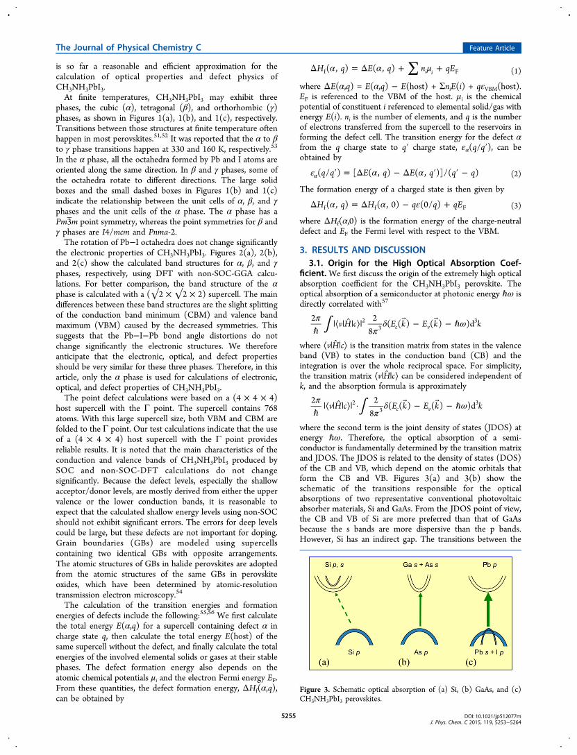
where the second term is the joint density of states (JDOS) atenergy ℏω. Therefore, the optical absorption of a semi-conductor is fundamentally determined by the transition matrixand JDOS. The JDOS is related to the density of states (DOS)of the CB and VB, which depend on the atomic orbitals thatform the CB and VB. Figures 3(a) and 3(b) show theschematic of the transitions responsible for the opticalabsorptions of two representative conventional photovoltaicabsorber materials, Si and GaAs. From the JDOS point of view,the CB and VB of Si are more preferred than that of GaAsbecause the s bands are more dispersive than the p bands.However, Si has an indirect gap. The transitions between the
Figure 3. Schematic optical absorption of (a) Si, (b) GaAs, and (c)CH3NH3PbI3 perovskites.
The Journal of Physical Chemistry C Feature Article
DOI: 10.1021/jp512077mJ. Phys. Chem. C 2015, 119, 5253−5264
5255
VB and CB edges require the assistance of phonons, leading toa rather inefficient optical absorption near the band edge. Theideal situation for efficient optical absorption is to combine thecharacteristics of Si and GaAs, i.e., to have p−p transitions anda direct band gap. The p−p transitions can only be possible forcompound semiconductors containing cation elements thatexhibit lone pair s electrons, such as Ge(2), Sn(2), Pb(2),Sb(3), and Bi(3). For example, SnS, PbS, Sb2Se3, Bi2S3, etc. arecompound semiconductors with p−p transitions. Unfortu-nately, these compounds usually have low symmetry andtherefore indirect band gaps. However, lead halide perovskitesnot only have p−p transitions but also have direct band gap,leading to highly efficient optical absorptions as depicted inFigure 3(c). Therefore, lead halide perovskites are expected toexhibit a high optical absorption coefficient, due to the Pb lone-pair s orbitals and the perovskite symmetry.To evaluate the high optical absorption of halide perovskites,
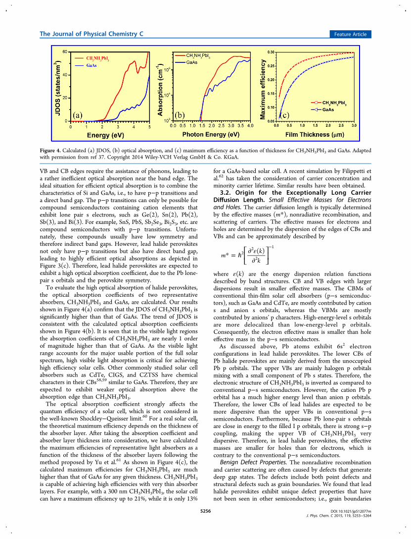
the optical absorption coefficients of two representativeabsorbers, CH3NH3PbI3 and GaAs, are calculated. Our resultsshown in Figure 4(a) confirm that the JDOS of CH3NH3PbI3 issignificantly higher than that of GaAs. The trend of JDOS isconsistent with the calculated optical absorption coefficientsshown in Figure 4(b). It is seen that in the visible light regionsthe absorption coefficients of CH3NH3PbI3 are nearly 1 orderof magnitude higher than that of GaAs. As the visible lightrange accounts for the major usable portion of the full solarspectrum, high visible light absorption is critical for achievinghigh efficiency solar cells. Other commonly studied solar cellabsorbers such as CdTe, CIGS, and CZTSS have chemicalcharacters in their CBs58,59 similar to GaAs. Therefore, they areexpected to exhibit weaker optical absorption above theabsorption edge than CH3NH3PbI3.The optical absorption coefficient strongly affects the
quantum efficiency of a solar cell, which is not considered inthe well-known Shockley−Queisser limit.60 For a real solar cell,the theoretical maximum efficiency depends on the thickness ofthe absorber layer. After taking the absorption coefficient andabsorber layer thickness into consideration, we have calculatedthe maximum efficiencies of representative light absorbers as afunction of the thickness of the absorber layers following themethod proposed by Yu et al.61 As shown in Figure 4(c), thecalculated maximum efficiencies for CH3NH3PbI3 are muchhigher than that of GaAs for any given thickness. CH3NH3PbI3is capable of achieving high efficiencies with very thin absorberlayers. For example, with a 300 nm CH3NH3PbI3, the solar cellcan have a maximum efficiency up to 21%, while it is only 13%
for a GaAs-based solar cell. A recent simulation by Filippetti etal.62 has taken the consideration of carrier concentration andminority carrier lifetime. Similar results have been obtained.
3.2. Origin for the Exceptionally Long CarrierDiffusion Length. Small Effective Masses for Electronsand Holes. The carrier diffusion length is typically determinedby the effective masses (m*), nonradiative recombination, andscattering of carriers. The effective masses for electrons andholes are determined by the dispersion of the edges of CBs andVBs and can be approximately described by
ε* = ℏ ∂∂
−⎡⎣⎢
⎤⎦⎥m
kk( )2
2
2
1
where ε(k) are the energy dispersion relation functionsdescribed by band structures. CB and VB edges with largerdispersions result in smaller effective masses. The CBMs ofconventional thin-film solar cell absorbers (p−s semiconduc-tors), such as GaAs and CdTe, are mostly contributed by cations and anion s orbitals, whereas the VBMs are mostlycontributed by anions’ p characters. High-energy-level s orbitalsare more delocalized than low-energy-level p orbitals.Consequently, the electron effective mass is smaller than holeeffective mass in the p−s semiconductors.As discussed above, Pb atoms exhibit 6s2 electron
configurations in lead halide perovskites. The lower CBs ofPb halide perovskites are mainly derived from the unoccupiedPb p orbitals. The upper VBs are mainly halogen p orbitalsmixing with a small component of Pb s states. Therefore, theelectronic structure of CH3NH3PbI3 is inverted as compared toconventional p−s semiconductors. However, the cation Pb porbital has a much higher energy level than anion p orbitals.Therefore, the lower CBs of lead halides are expected to bemore dispersive than the upper VBs in conventional p−ssemiconductors. Furthermore, because Pb lone-pair s orbitalsare close in energy to the filled I p orbitals, there is strong s−pcoupling, making the upper VB of CH3NH3PbI3 verydispersive. Therefore, in lead halide perovskites, the effectivemasses are smaller for holes than for electrons, which iscontrary to the conventional p−s semiconductors.
Benign Defect Properties. The nonradiative recombinationand carrier scattering are often caused by defects that generatedeep gap states. The defects include both point defects andstructural defects such as grain boundaries. We found that leadhalide perovskites exhibit unique defect properties that havenot been seen in other semiconductors; i.e., grain boundaries
Figure 4. Calculated (a) JDOS, (b) optical absorption, and (c) maximum efficiency as a function of thickness for CH3NH3PbI3 and GaAs. Adaptedwith permission from ref 37. Copyright 2014 Wiley-VCH Verlag GmbH & Co. KGaA.
The Journal of Physical Chemistry C Feature Article
DOI: 10.1021/jp512077mJ. Phys. Chem. C 2015, 119, 5253−5264
5256
and dominant point defects do not create deep levels and aretherefore electrically benign. Some point defects generate deepgap states; however, these defects have high formation energies,and their concentrations are expected to be low in synthesizedlead halide perovskite thin films. We further found that theseunique defect properties are attributed to the strong Pb lone-pair s−halogen p antibonding coupling, the ionic character-istics, and the large lattice constants.We first provide a qualitative understanding on the basic
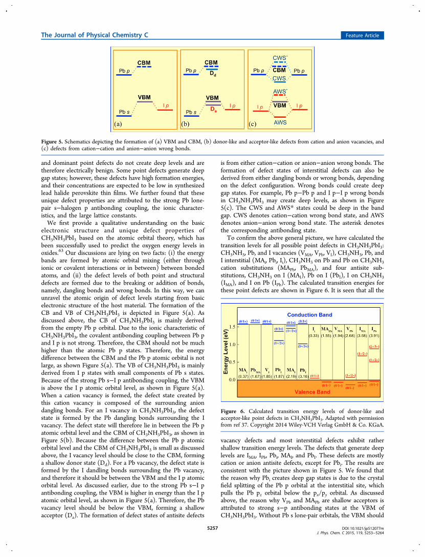
electronic structure and unique defect properties ofCH3NH3PbI3 based on the atomic orbital theory, which hasbeen successfully used to predict the oxygen energy levels inoxides.63 Our discussions are lying on two facts: (i) the energybands are formed by atomic orbital mixing (either throughionic or covalent interactions or in between) between bondedatoms, and (ii) the defect levels of both point and structuraldefects are formed due to the breaking or addition of bonds,namely, dangling bonds and wrong bonds. In this way, we canunravel the atomic origin of defect levels starting from basicelectronic structure of the host material. The formation of theCB and VB of CH3NH3PbI3 is depicted in Figure 5(a). Asdiscussed above, the CB of CH3NH3PbI3 is mainly derivedfrom the empty Pb p orbital. Due to the ionic characteristic ofCH3NH3PbI3, the covalent antibonding coupling between Pb pand I p is not strong. Therefore, the CBM should not be muchhigher than the atomic Pb p states. Therefore, the energydifference between the CBM and the Pb p atomic orbital is notlarge, as shown Figure 5(a). The VB of CH3NH3PbI3 is mainlyderived from I p states with small components of Pb s states.Because of the strong Pb s−I p antibonding coupling, the VBMis above the I p atomic orbital level, as shown in Figure 5(a).When a cation vacancy is formed, the defect state created bythis cation vacancy is composed of the surrounding aniondangling bonds. For an I vacancy in CH3NH3PbI3, the defectstate is formed by the Pb dangling bonds surrounding the Ivacancy. The defect state will therefore lie in between the Pb patomic orbital level and the CBM of CH3NH3PbI3, as shown inFigure 5(b). Because the difference between the Pb p atomicorbital level and the CBM of CH3NH3PbI3 is small as discussedabove, the I vacancy level should be close to the CBM, forminga shallow donor state (Dd). For a Pb vacancy, the defect state isformed by the I dandling bonds surrounding the Pb vacancy,and therefore it should be between the VBM and the I p atomicorbital level. As discussed earlier, due to the strong Pb s−I pantibonding coupling, the VBM is higher in energy than the I patomic orbital level, as shown in Figure 5(a). Therefore, the Pbvacancy level should be below the VBM, forming a shallowacceptor (Da). The formation of defect states of antisite defects
is from either cation−cation or anion−anion wrong bonds. Theformation of defect states of interstitial defects can also bederived from either dangling bonds or wrong bonds, dependingon the defect configuration. Wrong bonds could create deepgap states. For example, Pb p−Pb p and I p−I p wrong bondsin CH3NH3PbI3 may create deep levels, as shown in Figure5(c). The CWS and AWS* states could be deep in the bandgap. CWS denotes cation−cation wrong bond state, and AWSdenotes anion−anion wrong bond state. The asterisk denotesthe corresponding antibonding state.To confirm the above general picture, we have calculated the
transition levels for all possible point defects in CH3NH3PbI3:CH3NH3, Pb, and I vacancies (VMA, VPb, VI), CH3NH3, Pb, andI interstitial (MAi, Pbi, Ii), CH3NH3 on Pb and Pb on CH3NH3cation substitutions (MAPb, PbMA), and four antisite sub-stitutions, CH3NH3 on I (MAI), Pb on I (PbI), I on CH3NH3(IMA), and I on Pb (IPb). The calculated transition energies forthese point defects are shown in Figure 6. It is seen that all the
vacancy defects and most interstitial defects exhibit rathershallow transition energy levels. The defects that generate deeplevels are IMA, IPb, Pbi, MAI, and PbI. These defects are mostlycation or anion antisite defects, except for Pbi. The results areconsistent with the picture shown in Figure 5. We found thatthe reason why Pbi creates deep gap states is due to the crystalfield splitting of the Pb p orbital at the interstitial site, whichpulls the Pb pz orbital below the px/py orbital. As discussedabove, the reason why VPb and MAPb are shallow acceptors isattributed to strong s−p antibonding states at the VBM ofCH3NH3PbI3. Without Pb s lone-pair orbitals, the VBM should
Figure 5. Schematics depicting the formation of (a) VBM and CBM, (b) donor-like and acceptor-like defects from cation and anion vacancies, and(c) defects from cation−cation and anion−anion wrong bonds.
Figure 6. Calculated transition energy levels of donor-like andacceptor-like point defects in CH3NH3PbI3. Adapted with permissionfrom ref 37. Copyright 2014 Wiley-VCH Verlag GmbH & Co. KGaA.
The Journal of Physical Chemistry C Feature Article
DOI: 10.1021/jp512077mJ. Phys. Chem. C 2015, 119, 5253−5264
5257
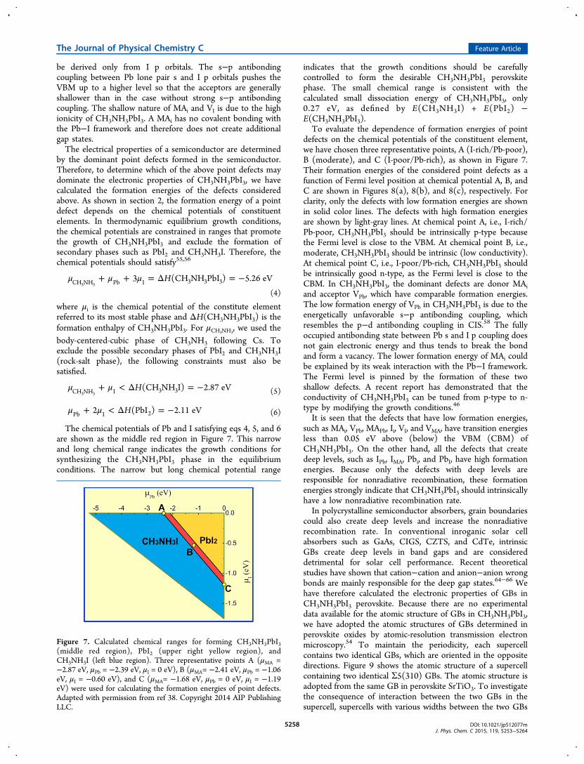
be derived only from I p orbitals. The s−p antibondingcoupling between Pb lone pair s and I p orbitals pushes theVBM up to a higher level so that the acceptors are generallyshallower than in the case without strong s−p antibondingcoupling. The shallow nature of MAi and VI is due to the highionicity of CH3NH3PbI3. A MAi has no covalent bonding withthe Pb−I framework and therefore does not create additionalgap states.The electrical properties of a semiconductor are determined
by the dominant point defects formed in the semiconductor.Therefore, to determine which of the above point defects maydominate the electronic properties of CH3NH3PbI3, we havecalculated the formation energies of the defects consideredabove. As shown in section 2, the formation energy of a pointdefect depends on the chemical potentials of constituentelements. In thermodynamic equilibrium growth conditions,the chemical potentials are constrained in ranges that promotethe growth of CH3NH3PbI3 and exclude the formation ofsecondary phases such as PbI2 and CH3NH3I. Therefore, thechemical potentials should satisfy55,56
μ μ μ+ + = Δ = −H3 (CH NH PbI ) 5.26 eVCH NH Pb I 3 3 33 3
(4)
where μi is the chemical potential of the constitute elementreferred to its most stable phase and ΔH(CH3NH3PbI3) is theformation enthalpy of CH3NH3PbI3. For μCH3NH3
, we used thebody-centered-cubic phase of CH3NH3 following Cs. Toexclude the possible secondary phases of PbI2 and CH3NH3I(rock-salt phase), the following constraints must also besatisfied.
μ μ+ < Δ = −H(CH NH I) 2.87 eVCH NH I 3 33 3 (5)
μ μ+ < Δ = −H2 (PbI ) 2.11 eVPb I 2 (6)
The chemical potentials of Pb and I satisfying eqs 4, 5, and 6are shown as the middle red region in Figure 7. This narrowand long chemical range indicates the growth conditions forsynthesizing the CH3NH3PbI3 phase in the equilibriumconditions. The narrow but long chemical potential range
indicates that the growth conditions should be carefullycontrolled to form the desirable CH3NH3PbI3 perovskitephase. The small chemical range is consistent with thecalculated small dissociation energy of CH3NH3PbI3, only0.27 eV, as defined by E(CH3NH3I) + E(PbI2) −E(CH3NH3PbI3).To evaluate the dependence of formation energies of point
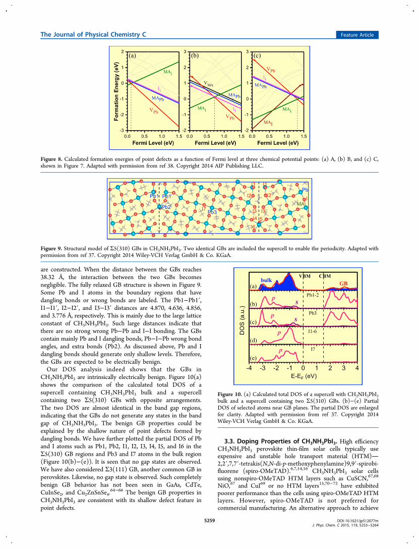
defects on the chemical potentials of the constituent element,we have chosen three representative points, A (I-rich/Pb-poor),B (moderate), and C (I-poor/Pb-rich), as shown in Figure 7.Their formation energies of the considered point defects as afunction of Fermi level position at chemical potential A, B, andC are shown in Figures 8(a), 8(b), and 8(c), respectively. Forclarity, only the defects with low formation energies are shownin solid color lines. The defects with high formation energiesare shown by light-gray lines. At chemical point A, i.e., I-rich/Pb-poor, CH3NH3PbI3 should be intrinsically p-type becausethe Fermi level is close to the VBM. At chemical point B, i.e.,moderate, CH3NH3PbI3 should be intrinsic (low conductivity).At chemical point C, i.e., I-poor/Pb-rich, CH3NH3PbI3 shouldbe intrinsically good n-type, as the Fermi level is close to theCBM. In CH3NH3PbI3, the dominant defects are donor MAiand acceptor VPb, which have comparable formation energies.The low formation energy of VPb in CH3NH3PbI3 is due to theenergetically unfavorable s−p antibonding coupling, whichresembles the p−d antibonding coupling in CIS.58 The fullyoccupied antibonding state between Pb s and I p coupling doesnot gain electronic energy and thus tends to break the bondand form a vacancy. The lower formation energy of MAi couldbe explained by its weak interaction with the Pb−I framework.The Fermi level is pinned by the formation of these twoshallow defects. A recent report has demonstrated that theconductivity of CH3NH3PbI3 can be tuned from p-type to n-type by modifying the growth conditions.46
It is seen that the defects that have low formation energies,such as MAi, VPb, MAPb, Ii, VI, and VMA, have transition energiesless than 0.05 eV above (below) the VBM (CBM) ofCH3NH3PbI3. On the other hand, all the defects that createdeep levels, such as IPb, IMA, Pbi, and PbI, have high formationenergies. Because only the defects with deep levels areresponsible for nonradiative recombination, these formationenergies strongly indicate that CH3NH3PbI3 should intrinsicallyhave a low nonradiative recombination rate.In polycrystalline semiconductor absorbers, grain boundaries
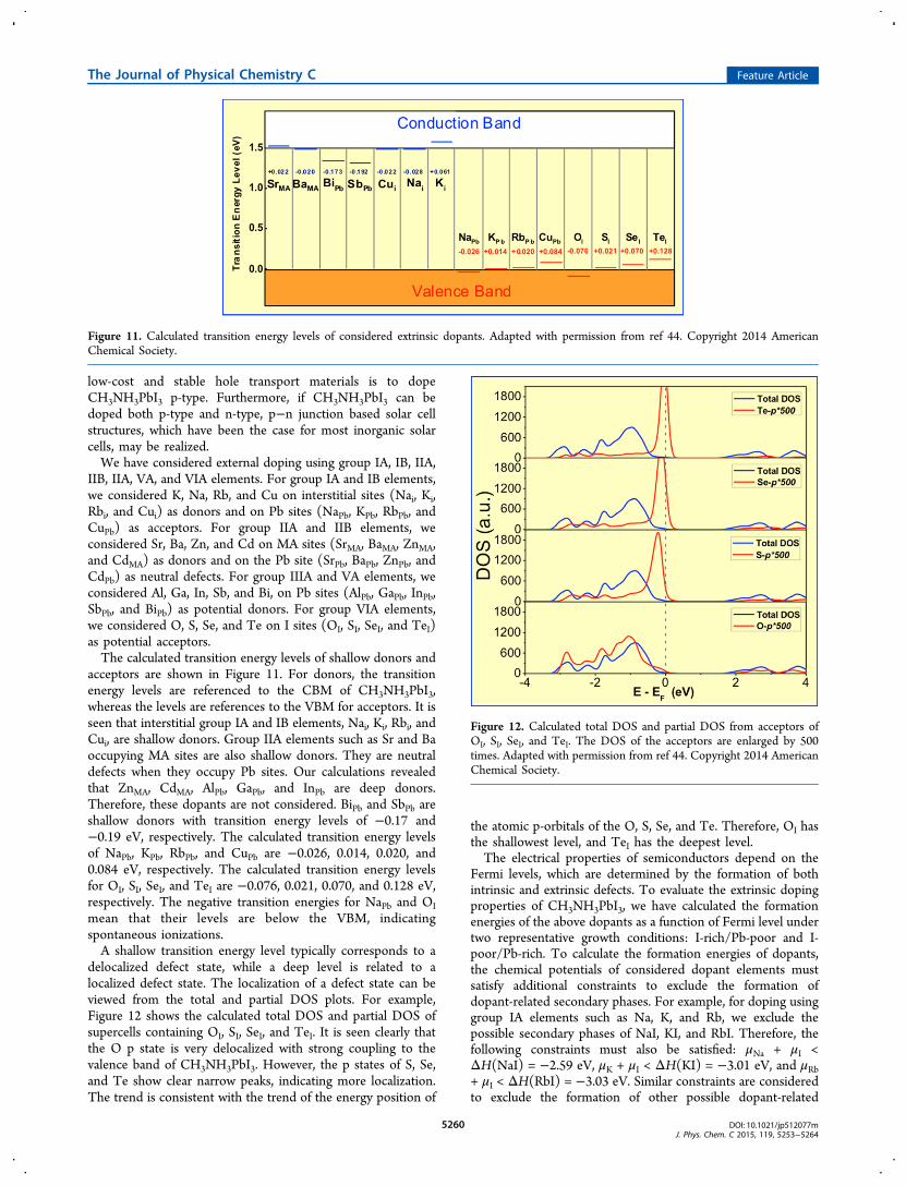
could also create deep levels and increase the nonradiativerecombination rate. In conventional inroganic solar cellabsorbers such as GaAs, CIGS, CZTS, and CdTe, intrinsicGBs create deep levels in band gaps and are considereddetrimental for solar cell performance. Recent theoreticalstudies have shown that cation−cation and anion−anion wrongbonds are mainly responsible for the deep gap states.64−66 Wehave therefore calculated the electronic properties of GBs inCH3NH3PbI3 perovskite. Because there are no experimentaldata available for the atomic structure of GBs in CH3NH3PbI3,we have adopted the atomic structures of GBs determined inperovskite oxides by atomic-resolution transmission electronmicroscopy.54 To maintain the periodicity, each supercellcontains two identical GBs, which are oriented in the oppositedirections. Figure 9 shows the atomic structure of a supercellcontaining two identical Σ5(310) GBs. The atomic structure isadopted from the same GB in perovskite SrTiO3. To investigatethe consequence of interaction between the two GBs in thesupercell, supercells with various widths between the two GBs
Figure 7. Calculated chemical ranges for forming CH3NH3PbI3(middle red region), PbI2 (upper right yellow region), andCH3NH3I (left blue region). Three representative points A (μMA =−2.87 eV, μPb = −2.39 eV, μI = 0 eV), B (μMA= −2.41 eV, μPb = −1.06eV, μI = −0.60 eV), and C (μMA= −1.68 eV, μPb = 0 eV, μI = −1.19eV) were used for calculating the formation energies of point defects.Adapted with permission from ref 38. Copyright 2014 AIP PublishingLLC.
The Journal of Physical Chemistry C Feature Article
DOI: 10.1021/jp512077mJ. Phys. Chem. C 2015, 119, 5253−5264
5258
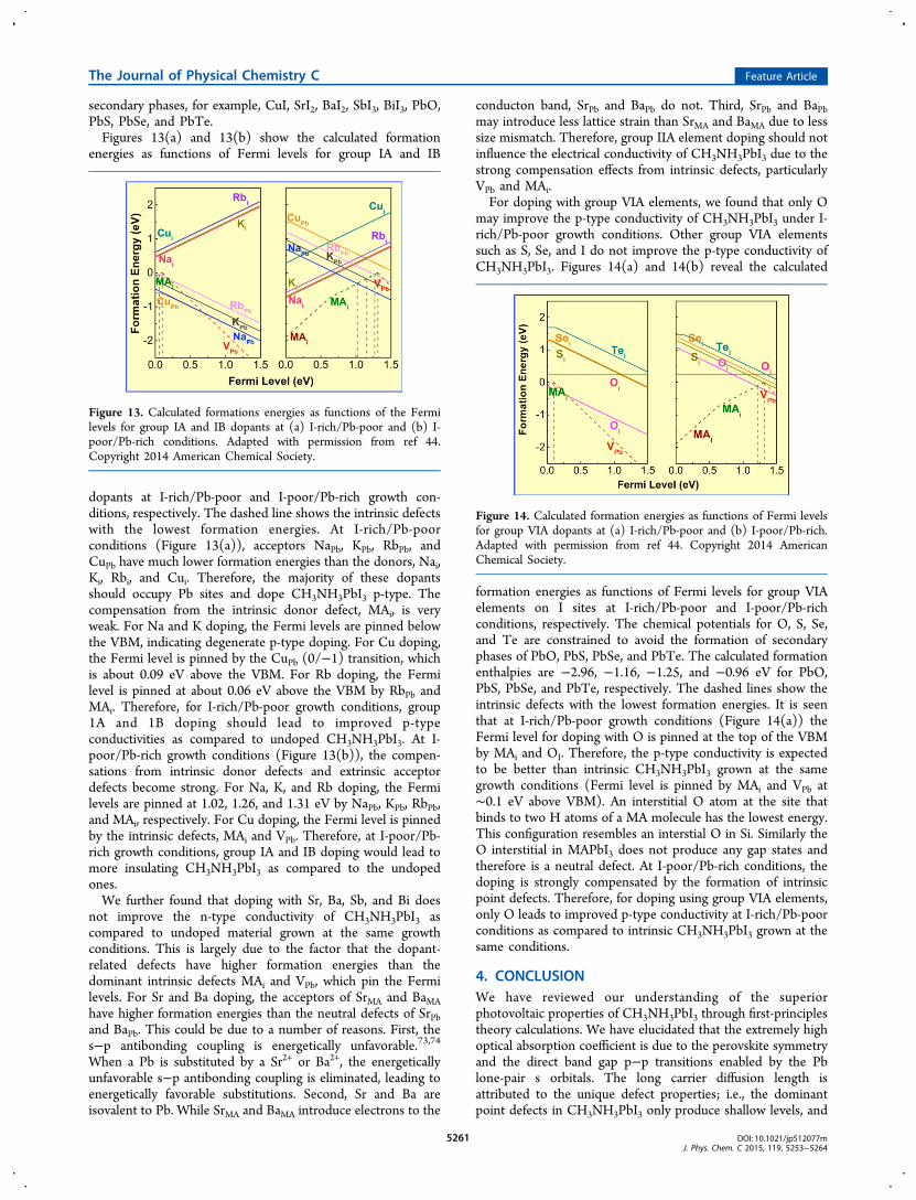
are constructed. When the distance between the GBs reaches38.32 Å, the interaction between the two GBs becomesnegligible. The fully relaxed GB structure is shown in Figure 9.Some Pb and I atoms in the boundary regions that havedangling bonds or wrong bonds are labeled. The Pb1−Pb1′,I1−I1′, I2−I2′, and I3−I3′ distances are 4.870, 4.636, 4.856,and 3.776 Å, respectively. This is mainly due to the large latticeconstant of CH3NH3PbI3. Such large distances indicate thatthere are no strong wrong Pb−Pb and I−I bonding. The GBscontain mainly Pb and I dangling bonds, Pb−I−Pb wrong bondangles, and extra bonds (Pb2). As discussed above, Pb and Idangling bonds should generate only shallow levels. Therefore,the GBs are expected to be electrically benign.Our DOS analysis indeed shows that the GBs in
CH3NH3PbI3 are intrinsically electrically benign. Figure 10(a)shows the comparison of the calculated total DOS of asupercell containing CH3NH3PbI3 bulk and a supercellcontaining two Σ5(310) GBs with opposite arrangements.The two DOS are almost identical in the band gap regions,indicating that the GBs do not generate any states in the bandgap of CH3NH3PbI3. The benign GB properties could beexplained by the shallow nature of point defects formed bydangling bonds. We have further plotted the partial DOS of Pband I atoms such as Pb1, Pb2, I1, I2, I3, I4, I5, and I6 in theΣ5(310) GB regions and Pb3 and I7 atoms in the bulk region(Figure 10(b)−(e)). It is seen that no gap states are observed.We have also considered Σ3(111) GB, another common GB inperovskites. Likewise, no gap state is observed. Such completelybenign GB behavior has not been seen in GaAs, CdTe,CuInSe2, and Cu2ZnSnSe4.
64−66 The benign GB properties inCH3NH3PbI3 are consistent with its shallow defect feature inpoint defects.
3.3. Doping Properties of CH3NH3PbI3. High efficiencyCH3NH3PbI3 perovskite thin-film solar cells typically useexpensive and unstable hole transport material (HTM)2,2′,7,7′-tetrakis(N,N-di-p-methoxyphenylamine)9,9′-spirobi-fluorene (spiro-OMeTAD).6,7,14,16 CH3NH3PbI3 solar cellsusing nonspiro-OMeTAD HTM layers such as CuSCN,67,68
NiO,67 and CuI69 or no HTM layers15,70−72 have exhibitedpoorer performance than the cells using spiro-OMeTAD HTMlayers. However, spiro-OMeTAD is not preferred forcommercial manufacturing. An alternative approach to achieve
Figure 8. Calculated formation energies of point defects as a function of Fermi level at three chemical potential points: (a) A, (b) B, and (c) C,shown in Figure 7. Adapted with permission from ref 38. Copyright 2014 AIP Publishing LLC.
Figure 9. Structural model of Σ5(310) GBs in CH3NH3PbI3. Two identical GBs are included the supercell to enable the periodicity. Adapted withpermission from ref 37. Copyright 2014 Wiley-VCH Verlag GmbH & Co. KGaA.
Figure 10. (a) Calculated total DOS of a supercell with CH3NH3PbI3bulk and a supercell containing two Σ5(310) GBs. (b)−(e) PartialDOS of selected atoms near GB planes. The partial DOS are enlargedfor clarity. Adapted with permission from ref 37. Copyright 2014Wiley-VCH Verlag GmbH & Co. KGaA.
The Journal of Physical Chemistry C Feature Article
DOI: 10.1021/jp512077mJ. Phys. Chem. C 2015, 119, 5253−5264
5259
low-cost and stable hole transport materials is to dopeCH3NH3PbI3 p-type. Furthermore, if CH3NH3PbI3 can bedoped both p-type and n-type, p−n junction based solar cellstructures, which have been the case for most inorganic solarcells, may be realized.We have considered external doping using group IA, IB, IIA,
IIB, IIA, VA, and VIA elements. For group IA and IB elements,we considered K, Na, Rb, and Cu on interstitial sites (Nai, Ki,Rbi, and Cui) as donors and on Pb sites (NaPb, KPb, RbPb, andCuPb) as acceptors. For group IIA and IIB elements, weconsidered Sr, Ba, Zn, and Cd on MA sites (SrMA, BaMA, ZnMA,and CdMA) as donors and on the Pb site (SrPb, BaPb, ZnPb, andCdPb) as neutral defects. For group IIIA and VA elements, weconsidered Al, Ga, In, Sb, and Bi, on Pb sites (AlPb, GaPb, InPb,SbPb, and BiPb) as potential donors. For group VIA elements,we considered O, S, Se, and Te on I sites (OI, SI, SeI, and TeI)as potential acceptors.The calculated transition energy levels of shallow donors and
acceptors are shown in Figure 11. For donors, the transitionenergy levels are referenced to the CBM of CH3NH3PbI3,whereas the levels are references to the VBM for acceptors. It isseen that interstitial group IA and IB elements, Nai, Ki, Rbi, andCui, are shallow donors. Group IIA elements such as Sr and Baoccupying MA sites are also shallow donors. They are neutraldefects when they occupy Pb sites. Our calculations revealedthat ZnMA, CdMA, AlPb, GaPb, and InPb are deep donors.Therefore, these dopants are not considered. BiPb and SbPb areshallow donors with transition energy levels of −0.17 and−0.19 eV, respectively. The calculated transition energy levelsof NaPb, KPb, RbPb, and CuPb are −0.026, 0.014, 0.020, and0.084 eV, respectively. The calculated transition energy levelsfor OI, SI, SeI, and TeI are −0.076, 0.021, 0.070, and 0.128 eV,respectively. The negative transition energies for NaPb and OImean that their levels are below the VBM, indicatingspontaneous ionizations.A shallow transition energy level typically corresponds to a
delocalized defect state, while a deep level is related to alocalized defect state. The localization of a defect state can beviewed from the total and partial DOS plots. For example,Figure 12 shows the calculated total DOS and partial DOS ofsupercells containing OI, SI, SeI, and TeI. It is seen clearly thatthe O p state is very delocalized with strong coupling to thevalence band of CH3NH3PbI3. However, the p states of S, Se,and Te show clear narrow peaks, indicating more localization.The trend is consistent with the trend of the energy position of
the atomic p-orbitals of the O, S, Se, and Te. Therefore, OI hasthe shallowest level, and TeI has the deepest level.The electrical properties of semiconductors depend on the
Fermi levels, which are determined by the formation of bothintrinsic and extrinsic defects. To evaluate the extrinsic dopingproperties of CH3NH3PbI3, we have calculated the formationenergies of the above dopants as a function of Fermi level undertwo representative growth conditions: I-rich/Pb-poor and I-poor/Pb-rich. To calculate the formation energies of dopants,the chemical potentials of considered dopant elements mustsatisfy additional constraints to exclude the formation ofdopant-related secondary phases. For example, for doping usinggroup IA elements such as Na, K, and Rb, we exclude thepossible secondary phases of NaI, KI, and RbI. Therefore, thefollowing constraints must also be satisfied: μNa + μI <ΔH(NaI) = −2.59 eV, μK + μI < ΔH(KI) = −3.01 eV, and μRb+ μI < ΔH(RbI) = −3.03 eV. Similar constraints are consideredto exclude the formation of other possible dopant-related
Figure 11. Calculated transition energy levels of considered extrinsic dopants. Adapted with permission from ref 44. Copyright 2014 AmericanChemical Society.
Figure 12. Calculated total DOS and partial DOS from acceptors ofOI, SI, SeI, and TeI. The DOS of the acceptors are enlarged by 500times. Adapted with permission from ref 44. Copyright 2014 AmericanChemical Society.
The Journal of Physical Chemistry C Feature Article
DOI: 10.1021/jp512077mJ. Phys. Chem. C 2015, 119, 5253−5264
5260
secondary phases, for example, CuI, SrI2, BaI2, SbI3, BiI3, PbO,PbS, PbSe, and PbTe.Figures 13(a) and 13(b) show the calculated formation
energies as functions of Fermi levels for group IA and IB
dopants at I-rich/Pb-poor and I-poor/Pb-rich growth con-ditions, respectively. The dashed line shows the intrinsic defectswith the lowest formation energies. At I-rich/Pb-poorconditions (Figure 13(a)), acceptors NaPb, KPb, RbPb, andCuPb have much lower formation energies than the donors, Nai,Ki, Rbi, and Cui. Therefore, the majority of these dopantsshould occupy Pb sites and dope CH3NH3PbI3 p-type. Thecompensation from the intrinsic donor defect, MAi, is veryweak. For Na and K doping, the Fermi levels are pinned belowthe VBM, indicating degenerate p-type doping. For Cu doping,the Fermi level is pinned by the CuPb (0/−1) transition, whichis about 0.09 eV above the VBM. For Rb doping, the Fermilevel is pinned at about 0.06 eV above the VBM by RbPb andMAi. Therefore, for I-rich/Pb-poor growth conditions, group1A and 1B doping should lead to improved p-typeconductivities as compared to undoped CH3NH3PbI3. At I-poor/Pb-rich growth conditions (Figure 13(b)), the compen-sations from intrinsic donor defects and extrinsic acceptordefects become strong. For Na, K, and Rb doping, the Fermilevels are pinned at 1.02, 1.26, and 1.31 eV by NaPb, KPb, RbPb,and MAi, respectively. For Cu doping, the Fermi level is pinnedby the intrinsic defects, MAi and VPb. Therefore, at I-poor/Pb-rich growth conditions, group IA and IB doping would lead tomore insulating CH3NH3PbI3 as compared to the undopedones.We further found that doping with Sr, Ba, Sb, and Bi does
not improve the n-type conductivity of CH3NH3PbI3 ascompared to undoped material grown at the same growthconditions. This is largely due to the factor that the dopant-related defects have higher formation energies than thedominant intrinsic defects MAi and VPb, which pin the Fermilevels. For Sr and Ba doping, the acceptors of SrMA and BaMAhave higher formation energies than the neutral defects of SrPband BaPb. This could be due to a number of reasons. First, thes−p antibonding coupling is energetically unfavorable.73,74
When a Pb is substituted by a Sr2+ or Ba2+, the energeticallyunfavorable s−p antibonding coupling is eliminated, leading toenergetically favorable substitutions. Second, Sr and Ba areisovalent to Pb. While SrMA and BaMA introduce electrons to the
conducton band, SrPb and BaPb do not. Third, SrPb and BaPbmay introduce less lattice strain than SrMA and BaMA due to lesssize mismatch. Therefore, group IIA element doping should notinfluence the electrical conductivity of CH3NH3PbI3 due to thestrong compensation effects from intrinsic defects, particularlyVPb and MAi.For doping with group VIA elements, we found that only O
may improve the p-type conductivity of CH3NH3PbI3 under I-rich/Pb-poor growth conditions. Other group VIA elementssuch as S, Se, and I do not improve the p-type conductivity ofCH3NH3PbI3. Figures 14(a) and 14(b) reveal the calculated
formation energies as functions of Fermi levels for group VIAelements on I sites at I-rich/Pb-poor and I-poor/Pb-richconditions, respectively. The chemical potentials for O, S, Se,and Te are constrained to avoid the formation of secondaryphases of PbO, PbS, PbSe, and PbTe. The calculated formationenthalpies are −2.96, −1.16, −1.25, and −0.96 eV for PbO,PbS, PbSe, and PbTe, respectively. The dashed lines show theintrinsic defects with the lowest formation energies. It is seenthat at I-rich/Pb-poor growth conditions (Figure 14(a)) theFermi level for doping with O is pinned at the top of the VBMby MAi and OI. Therefore, the p-type conductivity is expectedto be better than intrinsic CH3NH3PbI3 grown at the samegrowth conditions (Fermi level is pinned by MAi and VPb at∼0.1 eV above VBM). An interstitial O atom at the site thatbinds to two H atoms of a MA molecule has the lowest energy.This configuration resembles an interstial O in Si. Similarly theO interstitial in MAPbI3 does not produce any gap states andtherefore is a neutral defect. At I-poor/Pb-rich conditions, thedoping is strongly compensated by the formation of intrinsicpoint defects. Therefore, for doping using group VIA elements,only O leads to improved p-type conductivity at I-rich/Pb-poorconditions as compared to intrinsic CH3NH3PbI3 grown at thesame conditions.
4. CONCLUSIONWe have reviewed our understanding of the superiorphotovoltaic properties of CH3NH3PbI3 through first-principlestheory calculations. We have elucidated that the extremely highoptical absorption coefficient is due to the perovskite symmetryand the direct band gap p−p transitions enabled by the Pblone-pair s orbitals. The long carrier diffusion length isattributed to the unique defect properties; i.e., the dominantpoint defects in CH3NH3PbI3 only produce shallow levels, and
Figure 13. Calculated formations energies as functions of the Fermilevels for group IA and IB dopants at (a) I-rich/Pb-poor and (b) I-poor/Pb-rich conditions. Adapted with permission from ref 44.Copyright 2014 American Chemical Society.
Figure 14. Calculated formation energies as functions of Fermi levelsfor group VIA dopants at (a) I-rich/Pb-poor and (b) I-poor/Pb-rich.Adapted with permission from ref 44. Copyright 2014 AmericanChemical Society.
The Journal of Physical Chemistry C Feature Article
DOI: 10.1021/jp512077mJ. Phys. Chem. C 2015, 119, 5253−5264
5261
GBs are electrically benign. Such unique defect properties aredue to the large lattice constant, ionic characteristics, and strongantibonding coupling between Pb lone-pair s and I p orbitals.We have shown that CH3NH3PbI3 can be made with electricalconductivity from a good p-type to a good n-type via tuning thegrowth conditions. We have also shown that Na, K, Rb, and Odoping at I-rich growth conditions can improve the p-typeconductivity. However, n-type conductivity cannot be improvedthrough extrinsic doping due to strong compensations fromintrinsic defects.
■ AUTHOR INFORMATION
Corresponding Author*E-mail: [email protected]. Tel.: (1) 419 530 3918.
Notes
The authors declare no competing financial interest.
Biographies
Wan-Jian Yin received his B.S. in Physics (2004) and Ph.D. in
Theoretical Physics (2009) from Fudan University, China. He joined
the National Renewable Energy Laboratory (NREL) as a postdoctoral
researcher in 2009. He is currently holding a joint position of research
associate in NREL and research assistant professor in University of
Toledo. His research interests include energy-related materials and
defect physics in semiconductors.
Tingting Shi received a Ph.D. (2014) from The University of Toledo,
USA. She studied at the National Renewable Energy Laboratory for
one year before coming to The University of Toledo. She has been
working on computational study of photovoltaic materials.
Yanfa Yan has been an Ohio Research Scholar Chair and Professor inthe Department of Physics and Astronomy at The University ofToledo since 2011. Previously, he was a Principal Scientist at theNational Renewable Energy Laboratory. He earned his Ph.D. inPhysics from Wuhan University. His expertise includes theoreticalstudy of electronic properties and defect physics of semiconductorsand nanoscale characterization of microstructures, interfaces, anddefects in thin-film photovoltaic materials. He is a Fellow of theAmerican Physical Society.
■ ACKNOWLEDGMENTS
This work was supported by the U.S. Department of Energy(DOE) SunShot Initiative under the Next Generation Photo-voltaics 3 program (DE-FOA-0000990) and Ohio ResearchScholar Program. This research used the resources of the OhioSupercomputer Center and the National Energy ResearchScientific Computing Center, which is supported by the Officeof Science of the U.S. Department of Energy under ContractNo. DE-AC02-05CH11231.
■ REFERENCES(1) Kojima, A.; Teshima, K.; Shirai, Y.; Miyasaka, T. OrganometalHalide Perovskites as Visible-Light Sensitizers for Photovoltaic Cells. J.Am. Chem. Soc. 2009, 131, 6050−6051.(2) Im, J. H.; Lee, C. R.; Lee, J. W.; Park, S. W.; Park, N.-G. EfficientPerovskite Quantum-Dot-Sensitized Solar Cell. Nanoscale 2011, 3,4088−4093.(3) Kim, H.-S.; Lee, C.-R.; Im, J. H.; Lee, K. B.; Moehl, T.;Marchioro, A.; Moon, S. J.; Humphry-Baker, R.; Yum, J. H.; Moser, J.E.; et al. Lead Iodide Perovskite Sensitized All-Solid-State SubmicronThin Film Mesoscopic Solar Cell with Efficiency Exceeding 9%. Sci.Rep. 2012, 2, 591.(4) Chung, I.; Lee, B.; He, J. Q.; Chang, R. P. H.; Kanatzidis, M. G.All-Solid-State Dye-Sensitized Solar Cells with High Efficiency. Nature2012, 485, 486−489.(5) Lee, M. M.; Teuscher, J.; Miyasaka, T.; Murakami, T. N.; Snaith,H. J. Efficient Hybrid Solar Cells Based on Meso-SuperstructuredOrganometal Halide Perovskites. Science 2012, 338, 643−647.(6) Burschka, J.; Pellet, N.; Moon, S. J.; Humphry-Baker, R.; Gao, P.;Nazeeruddin, M. K.; Gratzel, M. Sequential Deposition as a Route toHigh-Performance Perovskite-Sensitized Solar Cells. Nature 2013,499, 316−319.(7) Liu, M. Z.; Johnston, M. B.; Snaith, H. J. Efficient PlanarHeterojunction Perovskite Solar Cells by Vapour Deposition. Nature2013, 501, 395−398.(8) Noh, J. H.; Im, S. H.; Heo, J. H.; Mandal, T. N.; Seok, S. I.Chemical Management for Colorful, Efficient, and Stable Inorganic−Organic Hybrid Nanostructured Solar Cells. Nano Lett. 2013, 13,1764−1769.
The Journal of Physical Chemistry C Feature Article
DOI: 10.1021/jp512077mJ. Phys. Chem. C 2015, 119, 5253−5264
5262
(9) Park, N. G. Organometal Perovskite Light Absorbers Toward a20% Efficiency Low-Cost Solid-State Mesoscopic Solar Cell. J. Phys.Chem. Lett. 2013, 4, 2423−2429.(10) Xing, G. C.; Mathews, N.; Sun, S. Y.; Lim, S. S.; Lam, Y. M.;Gratzel, M.; Mhaisalkar, S.; Sum, T. C. Long-Range Balanced Electron-and Hole-Transport Lengths in Organic-Inorganic CH3NH3PbI3.Science 2013, 342, 344−347.(11) Stranks, S. D.; Eperon, G. E.; Grancini, G.; Menelaou, C.;Alcocer, M. J. P.; Leijtens, T.; Herz, L. M.; Petrozza, A.; Snaith, H. J.Electron-Hole Diffusion Lengths Exceeding 1 Micrometer in anOrganometal Trihalide Perovskite Absorber. Science 2013, 342, 341−344.(12) Chen, Q.; Zhou, H.; Hong, Z.; Luo, S.; Duan, H.-S.; Wang, H.-H.; Liu, Y.; Li, G.; Yang, Y. Planar Heterojunction Perovskite SolarCells via Vapor-Assisted Solution Process. J. Am. Chem. Soc. 2014, 136,622−625.(13) http://www.nrel.gov/ncpv/images/efficiency_chart.jpg (ac-cessed on December 3, 2014).(14) Jeon, N. J.; Noh, J. H.; Kim, Y. C.; Yang, W. S.; Ryu, S.; Seok, S.I. Solvent Engineering for High-Performance Inorganic−OrganicHybrid Perovskite Solar Cells. Nat. Mater. 2014, 13, 897−903.(15) Mei, A.; Li, X.; Liu, L.; Ku, Z.; Liu, T.; Rong, Y.; Xu, M.; Hu, M.;Chen, J.; Yang, Y.; et al. A Hole-Conductor-Free, Fully PrintableMesoscopic Perovskite Solar Cell with High Stability. Science 2014,345, 295−298.(16) Zhou, H.; Chen, Q.; Li, G.; Luo, S.; Song, T.-B.; Hong, Z.; You,J.; Liu, Y.; Yang, Y. Interface Engineering of Highly Efficient PerovskiteSolar Cells. Science 2014, 345, 542−546.(17) Sun, S.; Salim, T.; Mathews, N.; Duchamp, M.; Boothhroyd, C.;Xing, G.; Sum, T.; Lam, Y. M. The Origin of High Efficiency in Low-Temperature Solution-Processable Bilayer Organometal HalideHybrid Solar Cells. Energy Environ. Sci. 2014, 7, 399−407.(18) Palik, E. D. Handbook of Optical Constants of Solids; AcademicPress: San Diego, CA, 1998.(19) De Wolf, S.; Holovsky, J.; Moon, S.-J.; Loper, P.; Niesen, B.;Ledinsky, M.; Haug, F.-J.; Yum, J.-H.; Baliff, C. Organometallic HalidePerovskite: Sharp Optical Absorption Edge and Its Relation toPhotovoltaic Performance. J. Phys. Chem. Lett. 2014, 5, 1035−1039.(20) Chang, Y. H.; Park, C. H.; Matsuishi, K. First-Principles Study ofthe Structural and the Electronic Properties of Lead-Halide-BasedInorganic-Organic Perovskites (CH3NH3)PbX3 and CsPbX3 (X = Cl,Br, I). J. Korean Phys. Soc. 2004, 44, 889−893.(21) Borriello, I.; Cantele, G.; Ninno, D. Ab initio Investigation ofHybrid Organic-Inorganic Perovskites Based on Tin Halides. Phys. Rev.B 2008, 77, 235214.(22) Murtaza, G.; Ahmad, I. First Principle Study of the Structuraland Optoelectronic Properties of Cubic Perovskites CsPbM3 (M=Cl,Br, I). Phys. B: Condens. Matter 2011, 406, 3222−3229.(23) Murtaza, G.; Ahmad, I.; Maqbool, M.; Aliabad, H. A. R.; Afaq, A.Structural and Optoelectronic Properties of Cubic CsPbF3 for NovelApplications. Chin. Phys. Lett. 2011, 28, 117803.(24) Even, J.; Pedesseau, L.; Dupertuis, M.-A.; Jancu, J.-M.; Katan, C.Electronic Model for Self-Assembled Hybrid Organic/PerovskiteSemiconductors: Reverse Band Edge Electronic States Ordering andSpin-Orbit Coupling. Phys. Rev. B 2012, 86, 205301−205304.(25) Mosconi, E.; Amat, A.; Nazeeruddin, M. K.; Gratzel, M.; DeAngelis, F. First-Principles Modeling of Mixed Halide OrganometalPerovskites for Photovoltaic Applications. J. Phys. Chem. C 2013, 117,13902−13913.(26) Even, J.; Pedesseau, L.; Jancu, J. M.; Katan, C. Importance ofSpin−Orbit Coupling in Hybrid Organic/Inorganic Perovskites forPhotovoltaic Applications. J. Phys. Chem. Lett. 2013, 4, 2999−3005.(27) Giorgi, G.; Fujisawa, J. I.; Segawa, H.; Yamashita, K. SmallPhotocarrier Effective Masses Featuring Ambipolar Transport inMethylammonium Lead Iodide Perovskite: A Density FunctionalAnalysis. J. Phys. Chem. Lett. 2013, 4, 4213−4216.(28) Umari, P.; Mosconi, E.; De Angelis, F. Relativistic GWCalculations on CH3NH3PbI3 and CH3NH3SnI3 Perovskites for SolarCell Applications. Sci. Rep. 2014, 4, 4464.
(29) Menendez-Proupin, E.; Palacios, P.; Wahnon, P.; Conesa, J. C.Self-Consistent Relativistic Band Structure of the CH3NH3PbI3Perovskite. Phys. Rev. B 2014, 90, 045207.(30) Brivio, F.; Butler, K. T.; Walsh, A.; van Schilfgaarde, M.Relativistic Quasiparticle Self-consistent Electronic Structure of HybridHalide Perovskite Photovoltaic Absorbers. Phys. Rev. B 2014, 89,155204.(31) Gottesman, R.; Haltzi, E.; Gouda, L.; Tirosh, S.; Bouhadana, Y.;Zaban, A. Extremely Slow Photoconductivity Response ofCH3NH3PbI3 Perovskites Suggesting Structural Changes underWorking Conditions. J. Phys. Chem. Lett. 2014, 5, 2662−2669.(32) Mosconi, E.; Ronca, E.; De Angelis, F. First-PrinciplesInvestigation of the TiO2/Organohalide Perovskites Interface: TheRole of Interfacial Chlorine. J. Phys. Chem. Lett. 2014, 5, 2619−2625.(33) Filippetti, A.; Mattoni, A. Hybrid Perovskites for Photovoltaics:Insights from First Principles. Phys. Rev. B 2014, 89, 125203.(34) Amat, A.; Mosconi, E.; Ronca, E.; Quarti, C.; Umari, P.;Nazeeruddin, M. K.; Gratzel, M.; De Angelis, F. Cation-Induced Band-Gap Tuning in Organohalide Perovskites: Interplay of Spin−OrbitCoupling and Octahedra Tilting. Nano Lett. 2014, 14, 3608−3616.(35) Haruyama, J.; Sodeyama, K.; Han, L.; Tateyama, Y. TerminationDependence of Tetragonal CH3NH3PbI3 Surfaces for Perovskite SolarCells. J. Phys. Chem. Lett. 2014, 5, 2903−2909.(36) Lang, L.; Yang, J.-H.; Liu, H. R.; Xiang, H. J.; Gong, X. G. First-Principles Study on the Electronic and Optical Properties of CubicABX3 Halide Perovskites. Phys. Lett. A 2014, 378, 290−293.(37) Yin, W.-J.; Shi, T.; Yan, Y. Unique Properties of HalidePerovskite Solar Cell Materials. Adv. Mater. 2014, 26, 4653−4658.(38) Yin, W.-J.; Shi, T.; Yan, Y. Unusual Defect Physics inCH3NH3PbI3 Perovskite Solar Cell Absorber. Appl. Phys. Lett. 2014,104, 063903.(39) Du, M. H. Efficient Carrier Transport in Halide Perovskites:Theoretical Perspectives. J. Mater. Chem. A 2014, 2, 9091−9098.(40) Agiorgousis, M. L.; Sun, Y.-Y.; Zeng, H.; Zhang, S. B. StrongCovalency-Induced Recombination Centers in Perovskite Solar CellMaterial CH3NH3PbI3. J. Am. Chem. Soc. 2014, 136, 14570−14575.(41) Xu, P.; Chen, S. Y.; Xiang, H.-J.; Gong, X.-G.; Wei, S.-H.Influence of Defects and Synthesis Conditions on the PhotovoltaicPerformance of Perovskite Semiconductor CsSnI3. Chem. Mater. 2014,26, 6068−6072.(42) Kim, J.; Lee, S.-H.; Lee, J. H.; Hong, K.-H. The Role of IntrinsicDefects in Methylammonium Lead Iodide Perovskite. J. Phys. Chem.Lett. 2014, 5, 1312−1317.(43) Buin, A.; Pietsch, P.; Xu, J.; Voznyy, O.; Ip, A. H.; Comin, R.;Sargent, E. H. Materials Processing Routes to Trap-Free HalidePerovskites. Nano Lett. 2014, 14, 6281−6286.(44) Shi, T.; Yin, W.-J.; Yan, Y. Predictions for p-Type CH3NH3PbI3Perovskites. J. Phys. Chem. C 2014, 118, 25350−25354.(45) Edri, E.; Kirmayer, S.; Mukhopadhyay, S.; Gartsman, K.; Hodes,G.; Cahen, D. Elucidating the Charge Carrier Separation and WorkingMechanism of CH3NH3PbI3‑xClx Perovskite Solar Cells. NatureCommun. 2014, 5, 3461.(46) Wang, Q.; Shao, Y.; Xie, H.; Lyu, L.; Liu, X.; Gao, Y.; Huang, J.Qualifying Composition Dependent p and n Self-doping inCH3NH3PbI3. Appl. Phys. Lett. 2014, 105, 163508.(47) Kresse, G.; Furthmuller, J. Efficient Iterative Schemes for abinitio Total-Energy Calculations Using a Plane-Wave Basis Set. Phys.Rev. B 1996, 54, 11169−11186.(48) Kresse, G.; Joubert, D. From Ultrasoft Pseudopotentials to theProjector Augmented-Wave Method. Phys. Rev. B 1999, 59, 1758−1775.(49) Perdew, J.; Burke, K.; Ernzerhof, M. Generalized GradientApproximation Made Simple. Phys. Rev. Lett. 1996, 77, 3865−3868.(50) Heyd, J.; Scuseria, G. E.; Ernzerhof, M. Hybrid FunctionalsBased on a Screened Coulomb Potential. J. Chem. Phys. 2003, 118,8207−8215.(51) Stoumpos, C. C.; Malliakas, C. D.; Kanatzidis, M. G.Semiconducting Tin and Lead Iodide Perovskites with Organic
The Journal of Physical Chemistry C Feature Article
DOI: 10.1021/jp512077mJ. Phys. Chem. C 2015, 119, 5253−5264
5263
Cations: Phase Transitions, High Mobilities, and Near-InfraredPhotoluminescent Properties. Inorg. Chem. 2013, 52, 9019−9038.(52) Baikie, T.; Fang, Y. N.; Kadro, J. M.; Schreyer, M.; Wei, F. X.;Mhaisalkar, S. G.; Graetzel, M.; White, T. J. Synthesis and CrystalChemistry of the Hybrid Perovskite (CH3NH3)PbI3 for Solid-StateSensitised Solar Cell Applications. J. Mater. Chem. A 2013, 1, 5628−5641.(53) Ball, J. M.; Lee, M. M.; Hey, A.; Snaith, H. J. Low-TemperatureProcessed Meso-Superstructured to Thin-Film Perovskite Solar Cells.Energy Environ. Sci. 2013, 6, 1739−1743.(54) Imaeda, M.; Mizoguchi, T.; Sato, Y.; Lee, H.-S.; Findlay, S. D.;Shibata, N.; Yamamoto, T.; Ikuhara, Y. Atomic Structure, ElectronicStructure, and Defect Energetics in [001](310)Σ5 Grain Boundaries ofSrTiO3 and BaTiO3. Phys. Rev. B 2008, 78, 245320.(55) Yan, Y.; Wei, S.-H. Doping Asymmetry in Wide-BandgapSemiconductors: Origins and Solutions. Phys. Status Solidi (b) 2008,245, 641−652.(56) Wei, S.-H. Overcoming the Doping Bottleneck in Semi-conductors. Comput. Mater. Sci. 2004, 30, 337−348.(57) Townsend, J. S. A Modern Approach to Quantum Mechanics;University Science Books: VA, 2012.(58) Zhang, S. B.; Wei, S.-H.; Zunger, A.; Katayama-Yoshida, H.Defect Physics of the CuInSe2 Chalcopyrite Semiconductor. Phys. Rev.B 1998, 57, 9642−9656.(59) Chen, S. Y.; Walsh, A.; Gong, X. G.; Wei, S. H. Classification ofLattice Defects in the Kesterite Cu2ZnSnS4 and Cu2ZnSnSe4 Earth-Abundant Solar Cell Absorbers. Adv. Mater. 2013, 25, 1522−1539.(60) Shockley, W.; Queisser, H. J. Detailed Balance Limit ofEfficiency of p-n Junction Solar Cells. J. Appl. Phys. 1961, 32, 510−519.(61) Yu, L.; Zunger, A. Identification of Potential PhotovoltaicAbsorbers Based on First-Principles Spectroscopic Screening ofMaterials. Phys. Rev. Lett. 2012, 108, 068701.(62) Filippetti, A.; Delugas, P.; Mattoni, A. Radiative Recombinationand Photoconversion of Methylammonium Lead-Iodide Perovskite byFirst-Principles: The Properties of an Inorganic Semiconductor withina Hybrid Body. J. Phys. Chem. C 2014, 118, 24843−24853.(63) Yin, W.-J.; Wei, S.-H.; Al-Jassim, M. M.; Yan, Y. Prediction ofthe Chemical Trends of Oxygen Vacancy Levels in Binary MetalOxides. Appl. Phys. Lett. 2011, 99, 142109.(64) Li, C.; Wu, Y.; Poplawsky, J.; Pennycook, T. J.; Paudel, N.; Yin,W.; Haigh, S. J.; Oxley, M. P.; Lupini, A. R.; Al-Jassim, M. M.; et al.Grain-Boundary-Enhanced Carrier Collection in CdTe Solar Cells.Phys. Rev. Lett. 2014, 112, 156103.(65) Yin, W.-J.; Wu, Y.; Noufi, R.; Al-Jassim, M. M.; Yan, Y. DefectSegregation at Grain Boundary and its Impact on PhotovoltaicPerformance of CuInSe2. Appl. Phys. Lett. 2013, 102, 193905.(66) Yin, W.-J.; Wu, Y.; Wei, S.-H.; Noufi, R.; Al-Jassim, M. M.; Yan,Y. Engineering Grain Boundaries in Cu2ZnSnSe4 for Better CellPerformance: A First Principles Study. Adv. Energy Mater. 2014, 4,1300712.(67) Subbiah, A. S.; Halder, A.; Ghosh, S.; Mahuli, N.; Hodes, G.;Sarkar, S. K. Inorganic Hole Conducting Layers for Perovskite-BasedSolar Cells. J. Phys. Chem. Lett. 2014, 5, 1748−1753.(68) Qin, P.; Tanaka, S.; Ito, S.; Tetrault, N.; Manabe, K.; Nishino,H.; Nazeeruddin, M. K.; Gratzel, M. Inorganic Hole Conductor-BasedLead Halide Perovskite Solar Cells with 12.4% Conversion Efficiency.Nature Commun. 2014, 5, 3834.(69) Christians, J. A.; Fung, R. C. M.; Kamat, P. V. An InorganicHole Conductor for Organo-Lead Halide Perovskite Solar Cells.Improved Hole Conductivity with Copper Iodide. J. Am. Chem. Soc.2014, 136, 758−764.(70) Laban, W. A.; Etgar, L. Depleted Hole Conductor-Free LeadHalide Iodide Heterojunction Solar Cells. Energy Environ. Sci. 2013, 6,3249−3253.(71) Aharon, S.; Gamliel, S.; Cohen, B. E.; Etgar, L. DepletionRegion Effect of Highly Efficient Hole Conductor Free CH3NH3PbI3Perovskite Solar Cells. Phys. Chem. Chem. Phys. 2014, 16, 10512−10518.
(72) Shi, J.; Dong, J.; Lv, S.; Xu, Y.; Zhu, L.; Xiao, J.; Xu, X.; Wu, H.;Li, D.; Luo, Y.; et al. Hole-Conductor-Free Perovskite Organic LeadIodide Heterojunction Thin-film Solar Cells: High Efficiency andJunction Property. Appl. Phys. Lett. 2014, 104, 063901.(73) Brivo, F.; Walker, A. B.; Walsh, A. Structural and ElectronicProperties of Hybrid Perovskites for High-Efficiency Thin-FilmPhotovoltaics from First-Principles. APL Mater. 2013, 1, 042111.(74) Wang, Y.; Gould, T.; Dobson, J.; Zhang, H.; Yan, H.; Yao, X.;Zhao, H. Density Functional Theory Analysis of Structural andElectronic Properties of Orthorhombic Perovskite CH3NH3PbI3. Phys.Chem. Chem. Phys. 2014, 16, 1424−1429.
The Journal of Physical Chemistry C Feature Article
DOI: 10.1021/jp512077mJ. Phys. Chem. C 2015, 119, 5253−5264
5264

![Modelingof Lead Halide Perovskites for Photovoltaic ... · arXiv:1405.1706v2 [cond-mat.mtrl-sci] 21 May 2014 Modelingof Lead Halide Perovskites for Photovoltaic Applications Radi](https://img.pdfslide.us/doc/110x75/5eabaa512754357de30f537e/modelingof-lead-halide-perovskites-for-photovoltaic-arxiv14051706v2-cond-matmtrl-sci.jpg)