Embed Size (px)
Citation preview

SUPERCONDUCTIVITY AND PHYSICS OF NANOMATERIALS
Prepared by P G LOGAN, Dept of Physics, SISTK, Puttur. Page 1
SUPERCONDUCTIVITY
Introduction
The phenomenon of attaining zero resistivity or infinite conductivity at low
temperature is known as superconductivity. The material becomes a super
conductor and it will be in super conducting state.
Superconductivity was first observed by kammerlingh
Onnes in the case of mercury. When the temperature of
mercury is decreased then the resistance also decreases and it
is nearly to zero at 4.2 K.
The temperature at which the material undergoes a
transition from normal state to super conducting state is known
as critical temperature or transition temperature (TC).
Properties
1. Superconductivity is a low temperature phenomenon.
2. The transition from normal state to superconducting state occurs below the critical temperature.
3. Different materials will have different critical temperatures.
4. The current once setup in a superconductor persists for a long time due to zero resistivity.
5 superconductors do not allow magnetic field through them and behaves a diamagnetic. This property of expulsion of magnetic field is known as Meissner effect.
6. The magnetic field at which a superconductor loses it‟s superconductivity and becomes a normal conductor is known as critical magnetic field HC.
7. The induced current in a superconductor induces a magnetic field in it. If the magnetic field is equal to the critical magnetic field then it converts into a normal conductor. The current in it is known as critical current (IC). If „r‟ is the radius of the super conductor then
𝐼𝐶 = 2𝜋𝑟𝐻𝐶
The current density at which it occurs is known as critical current density and is given by JC = IC/A, where A is the area of cross section of the super conductor.
8. Superconductivity occurs in metallic elements in which the number of valence electrons lies between 2 and 8.
9. Materials having high normal resistivity exhibit super conductivity.
10. Superconducting materials are not good conductors at room temperature.

SUPERCONDUCTIVITY AND PHYSICS OF NANOMATERIALS
Prepared by P G LOGAN, Dept of Physics, SISTK, Puttur. Page 2
Critical magnetic field (HC)
When a magnetic field is applied to a superconductor then for a particular value of applied field it loses superconductivity and becomes a normal conductor. The magnetic field for which a superconductor becomes a normal conductor is known as Critical magnetic field (HC) and is given by
𝐻𝐶 = 𝐻0 1 − 𝑇
𝑇𝐶 2
Where H0 is the field required to destroy the superconducting property at 0 K, TC is the critical temperature of the superconductor and T is the temperature of the super conductor.
Meissner Effect
When a weak magnetic field is applied to a superconducting specimen at a temperature below transition temperature TC, the magnetic flux lines are expelled. The specimen acts as an ideal diamagnet. This effect is called Meissner effect. This effect is reversible. Under this condition, the magnetic induction inside the specimen is given by
𝐵 = 𝜇0 𝐻 +𝑀
Where H is the external applied magnetic field and M is the magnetization produced inside the specimen.
When the specimen is superconducting according to Meissner effect, inside the bulk superconductor B = 0. Hence
0 = 𝜇0 𝐻 +𝑀
𝑀 = −𝐻
Thus the material is perfectly diamagnetic. Magnetic susceptibility can be expressed as
𝜒 =𝑀
𝐻= −1
London penetration depth
Consider a super conductor for which a magnetic field H0 is applied to one of its faces. To obey Meissner effect, it will not allow magnetic lines to pass through it, but in practice a small portion of H0 penetrates to a small distance into the superconductor.
The penetrating field at a distance 𝑥 from the face is given by
𝐻 = 𝐻0𝑒−𝑥 𝜆

SUPERCONDUCTIVITY AND PHYSICS OF NANOMATERIALS
Prepared by P G LOGAN, Dept of Physics, SISTK, Puttur. Page 3
Where 𝜆 is known as penetration depth. When 𝑥 = 𝜆, then 𝐻 = 𝐻0 𝑒 . The 𝜆 is the distance inside the super conductor at which the penetrating magnetic field is equal to 1/e times the applied magnetic field H0. 𝜆 Ranges from 10 to 100 nm. This depth is significant for a thin film superconductor rather than a bulk superconductor. The variation of 𝜆 with temperature T is given by
𝜆 =𝜆0
1− 𝑇
𝑇𝐶 4
1 2
Types of super conductor
In the presence of critical magnetic field, a superconductor convents into a normal conductor. Based on the conversion process, superconductors are classified into two types.
1. Type I super conductor
2. Type II super conductor
Type I super conductor
Consider a cylindrical superconductor to which a magnetic field H is applied along the axis of it. It will not allow the magnetic lines and obeys Meissner effect. Inside the super conductor, the magnetization acting opposite to H opposes the field. When the magnetic field is equal to the critical field Hc then immediately – M becomes zero & converts into normal conductor. Here, conversion is fast and is known as Type I superconductor. It is also known as soft super conductor.
Ex : Sn, Hg, Nb, V, etc
Type II superconductor
Consider a spherical superconductor in the magnetic field H. As per Meissner
effect, it expels the magnetic line and 𝐻 = −𝑀 . The curved magnetic lines are concentrated at the two ends marked as θ in such that intensity H is predominant at those ends. Up to lower critical field (𝐻𝐶1 ) it behaves as a super conductor. When the
magnetic field exceeds 𝐻𝐶1 , then the penetration starts at those ends marked as θ
This is because the intensity at those ends reaches 𝐻𝐶1value at first. As a aresult –𝑀
value decreases and the penetrated portion loses superconductivity and becomes a normal conductor. This conversion is usually completed at 𝐻𝐶2where the penetration
SUPERCONDUCTIVITY AND PHYSICS OF NANOMATERIALS
Prepared by P G LOGAN, Dept of Physics, SISTK, Puttur. Page 4
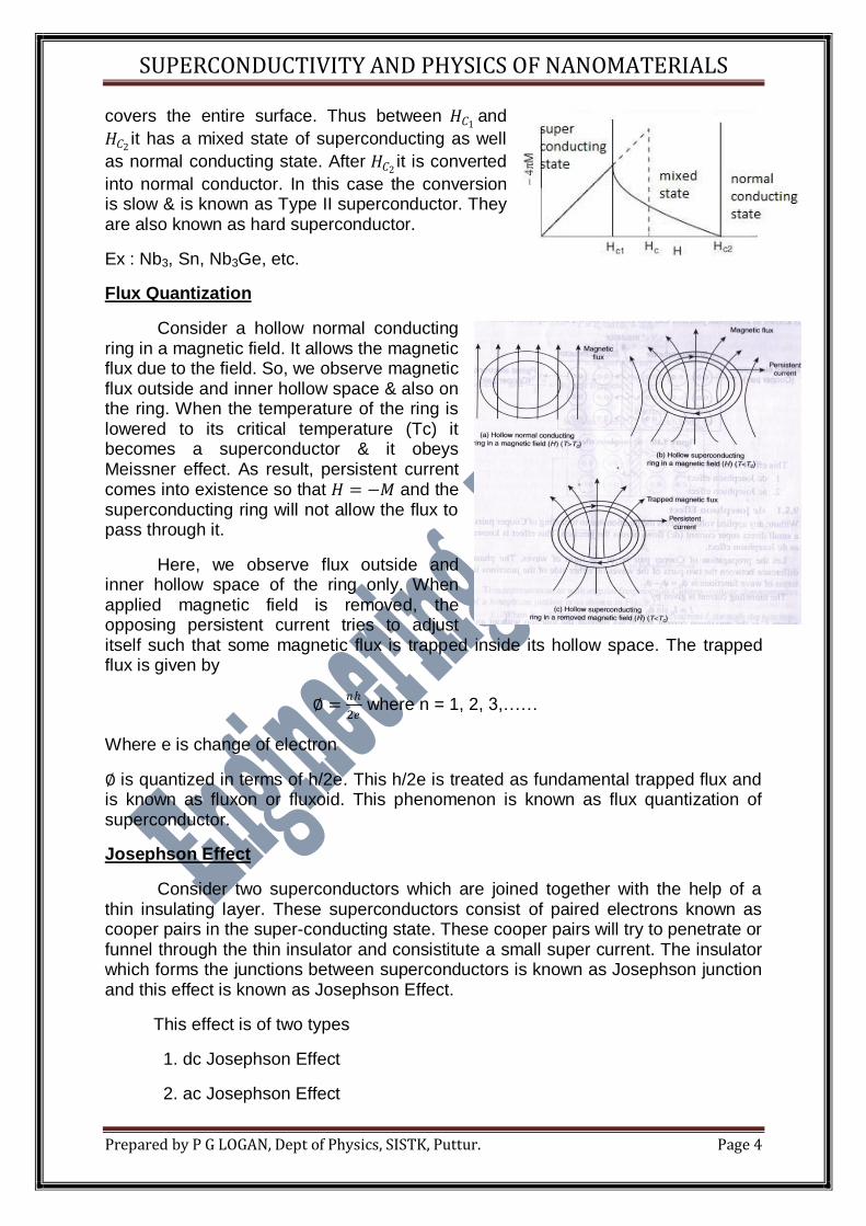
covers the entire surface. Thus between 𝐻𝐶1 and
𝐻𝐶2 it has a mixed state of superconducting as well
as normal conducting state. After 𝐻𝐶2 it is converted
into normal conductor. In this case the conversion is slow & is known as Type II superconductor. They are also known as hard superconductor.
Ex : Nb3, Sn, Nb3Ge, etc.
Flux Quantization
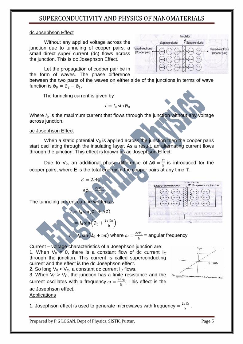
Consider a hollow normal conducting ring in a magnetic field. It allows the magnetic flux due to the field. So, we observe magnetic flux outside and inner hollow space & also on the ring. When the temperature of the ring is lowered to its critical temperature (Tc) it becomes a superconductor & it obeys Meissner effect. As result, persistent current comes into existence so that 𝐻 = −𝑀 and the superconducting ring will not allow the flux to pass through it.
Here, we observe flux outside and inner hollow space of the ring only. When applied magnetic field is removed, the opposing persistent current tries to adjust itself such that some magnetic flux is trapped inside its hollow space. The trapped flux is given by
∅ =𝑛ℎ
2𝑒 where n = 1, 2, 3,……
Where e is change of electron
∅ is quantized in terms of h/2e. This h/2e is treated as fundamental trapped flux and is known as fluxon or fluxoid. This phenomenon is known as flux quantization of superconductor.
Josephson Effect
Consider two superconductors which are joined together with the help of a thin insulating layer. These superconductors consist of paired electrons known as cooper pairs in the super-conducting state. These cooper pairs will try to penetrate or funnel through the thin insulator and consistitute a small super current. The insulator which forms the junctions between superconductors is known as Josephson junction and this effect is known as Josephson Effect.
This effect is of two types
1. dc Josephson Effect
2. ac Josephson Effect
SUPERCONDUCTIVITY AND PHYSICS OF NANOMATERIALS
Prepared by P G LOGAN, Dept of Physics, SISTK, Puttur. Page 5
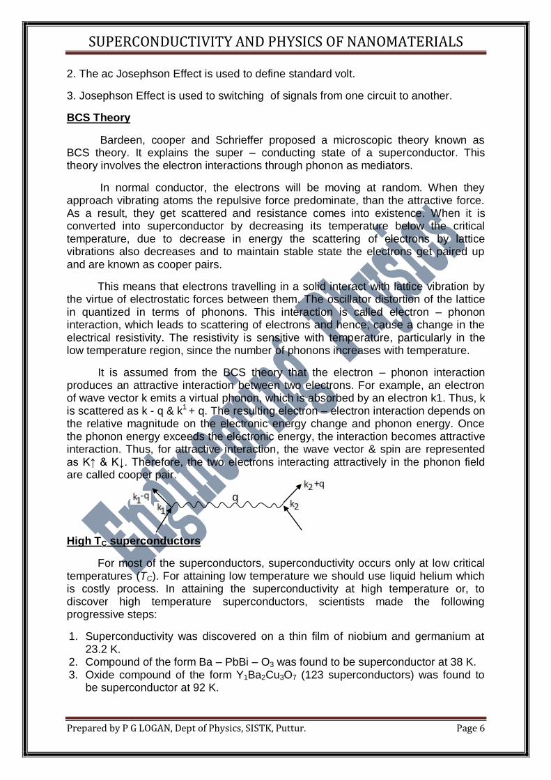
dc Josephson Effect
Without any applied voltage across the junction due to tunneling of cooper pairs, a small direct super current (dc) flows across the junction. This is dc Josephson Effect.
Let the propagation of cooper pair be in the form of waves. The phase difference between the two parts of the waves on either side of the junctions in terms of wave function is ∅0 = ∅2 − ∅1.
The tunneling current is given by
𝐼 = 𝐼0 sin∅0
Where 𝐼0 is the maximum current that flows through the junction without any voltage across junction.
ac Josephson Effect
When a static potential V0 is applied across the junction then the cooper pairs start oscillating through the insulating layer. As a result, an alternating current flows through the junction. This effect is known as ac Josephson Effect.
Due to V0, an additional phase difference of ∆∅ =𝐸𝑡
ħ is introduced for the
cooper pairs, where E is the total energy of the cooper pairs at any time „t‟.
𝐸 = 2𝑒𝑉0
∆∅ =2𝑒𝑉0𝑡
ħ
The tunneling current can be written as
𝐼 = 𝐼0 sin ∅0 + ∆∅
= 𝐼0 sin ∅0 +2𝑒𝑉0𝑡
ħ
𝐼 = 𝐼0 sin ∅0 +𝜔𝑡 where 𝜔 =2𝑒𝑉0
ħ = angular frequency
Current – voltage characteristics of a Josephson junction are: 1. When V0 = 0, there is a constant flow of dc current IC through the junction. This current is called superconducting current and the effect is the dc Josephson effect. 2. So long V0 < VC, a constant dc current IC flows. 3. When V0 > VC, the junction has a finite resistance and the
current oscillates with a frequency 𝜔 =2𝑒𝑉0
ħ. This effect is the
ac Josephson effect. Applications
1. Josephson effect is used to generate microwaves with frequency =2𝑒𝑉0
ħ .
SUPERCONDUCTIVITY AND PHYSICS OF NANOMATERIALS
Prepared by P G LOGAN, Dept of Physics, SISTK, Puttur. Page 6
2. The ac Josephson Effect is used to define standard volt.
3. Josephson Effect is used to switching of signals from one circuit to another.
BCS Theory
Bardeen, cooper and Schrieffer proposed a microscopic theory known as BCS theory. It explains the super – conducting state of a superconductor. This theory involves the electron interactions through phonon as mediators.
In normal conductor, the electrons will be moving at random. When they approach vibrating atoms the repulsive force predominate, than the attractive force. As a result, they get scattered and resistance comes into existence. When it is converted into superconductor by decreasing its temperature below the critical temperature, due to decrease in energy the scattering of electrons by lattice vibrations also decreases and to maintain stable state the electrons get paired up and are known as cooper pairs.
This means that electrons travelling in a solid interact with lattice vibration by the virtue of electrostatic forces between them. The oscillator distortion of the lattice in quantized in terms of phonons. This interaction is called electron – phonon interaction, which leads to scattering of electrons and hence, cause a change in the electrical resistivity. The resistivity is sensitive with temperature, particularly in the low temperature region, since the number of phonons increases with temperature.
It is assumed from the BCS theory that the electron – phonon interaction produces an attractive interaction between two electrons. For example, an electron of wave vector k emits a virtual phonon, which is absorbed by an electron k1. Thus, k is scattered as k - q & k1 + q. The resulting electron – electron interaction depends on the relative magnitude on the electronic energy change and phonon energy. Once the phonon energy exceeds the electronic energy, the interaction becomes attractive interaction. Thus, for attractive interaction, the wave vector & spin are represented as K↑ & K↓. Therefore, the two electrons interacting attractively in the phonon field are called cooper pair.
q
High TC superconductors
For most of the superconductors, superconductivity occurs only at low critical temperatures (TC). For attaining low temperature we should use liquid helium which is costly process. In attaining the superconductivity at high temperature or, to discover high temperature superconductors, scientists made the following progressive steps:
1. Superconductivity was discovered on a thin film of niobium and germanium at 23.2 K.
2. Compound of the form Ba – PbBi – O3 was found to be superconductor at 38 K. 3. Oxide compound of the form Y1Ba2Cu3O7 (123 superconductors) was found to
be superconductor at 92 K.
SUPERCONDUCTIVITY AND PHYSICS OF NANOMATERIALS
Prepared by P G LOGAN, Dept of Physics, SISTK, Puttur. Page 7
4. Oxide compound of the form Bi – Sr – Ca – Cu – O was found to be superconductor at 115 K.
5. The form Ti – Ba – Ca – Cu – O was found to be superconductor at 125 K.
In this high temperature superconductors phenomenon, liquid nitrogen (77 K) is used which is safer than liquid helium (4 K) or liquid hydrogen (23 K). It has been understood that oxygen atoms playa a major role in high temperature superconductors. Most of them have layered structure of copper and oxygen atoms.
Properties
1. They are highly anisotropic. 2. They have the presence of CuO3 layers. 3. They have inherent metallic properties.
Application of superconductors
Electric generators
Super – conducting generators are smaller in size, with less weight, consume very low energy. The low – loss super – conducting coil is rotated in a strong magnetic field. This is the basis of new generation of energy saving power system.
Magnetic levitation
Diamagnetic property of a superconductor is the basis of magnetic levitation. This effect can be used for the high speed transportation.
Low loss transmission lines and transformers
When super – conducting wires are used as electric cables then the transmission losses are minimized. If superconductors are used for winding of transformer, the power losses will be very small.
Generation of high magnetic fields
Superconducting materials are used for producing high magnetic fields with low power consumption.
Fast electrical switching
The application of magnetic field greater than HC, changes the superconducting state to normal state and removal of the field reverse the process. This principle is used in switching element cryotrons.
Logic and storage functions in computers
The C – V characteristics of Josephson Effect is used for memory elements in computers. Thus, superconductors are sued to perform logic and storage functions in computers.
Superconducting Quantum Interface Devices (SQUIDS)
Two Josephson junctions mounted on a superconducting ring form SQUID. These are used to study tiny magnetic signals from the brain and heart.

SUPERCONDUCTIVITY AND PHYSICS OF NANOMATERIALS
Prepared by P G LOGAN, Dept of Physics, SISTK, Puttur. Page 8
Superconducting magnets
Superconducting magnets consists of coils of wires made up of superconductors. Current once introduced into the coil, remains for a very long time causing the stability of the magnetic field for a long time. These coils can be used in electric machines, transformers.
PHYSICS OF NANOMATERIALS
Introduction
In 1959, Richard Feynman made a statement „there is plenty of room at the
bottom‟. Based on his study he manipulated smaller units of matter. He prophesied
that “we can arrange the atoms the way we want, the very atoms, all the way down”.
The term „nanotechnology‟ was coined by Norio Taniguchi at the University of Tokyo.
Nano means 10-9. A nano metre is one thousand millionth of a metre (i.e. 10-9 m).
The four kinds of scales
Name of the scale Range of the scale
Macroscopic 10 m – 10 mm
Mesoscopic 10 mm – 10 µm
Microscopic 100 µm – 100 nm
Nanoscopic 100 nm - 100 pm
Nanoscale
Nanoscale science deals with the study of phenomena at a very small scale of the range 10-7 m to 10-9 m. At the nanoscale, we are manipulating odjects that are more than one-millionth the size of the era.
A typical atom is any where from 0.1nm to 0.5 nm in diameters.
DNA molecules are about 2.5 nm nanometers wide.
A bacterium is about 1000 nm.
A RBC is 7000 nm in diameter and a water molecule is almost 0.3 nm across.
The size of a virus is 100 nm.
Nanoscience
It can be defined as the study of phenomena and manipulation of materials at
atomic, molecular and macromolecular scales, where properties differ significantly
from those at a larger scale.
Nanotechnology
It can be defined as the design, characterization, production and application of
structures, devices and systems by controlling shape and size at the nano metre
scale. It is also defined as “A branch of engineering that deals with the design and
manufacture of extremely small electronic circuits and mechanical devices built at
SUPERCONDUCTIVITY AND PHYSICS OF NANOMATERIALS
Prepared by P G LOGAN, Dept of Physics, SISTK, Puttur. Page 9
molecular level of matter. Now nanotechnology crosses and unites academic fields
such as Physics, Chemistry and Computer science.
Nanomaterials
Nanomaterials could be defined as those materials which have structured
components with size less than 100nm at least in one dimension. Any bulk material
we take, its size can express in 3-dimensions. Any planer material, its area can be
expressed in 2-dimension. Any linear material, its length can be expressed in 1-
dimension.
Materials that are nanoscale in 1-dimension or layers, such as thin films or
surface coatings.
Materials that are nanoscale in 2-dimensions include nanowires and
nanotubes.
Materials that are nanoscale in 3- dimensions are particles like precipitates,
colloids and quantum dots.
Significance of the nanoscale
The nanomaterials reduced to the nanoscale exhibit different properties
compared to what they exhibit on a macroscale. For example, opaque substances
become transparent (copper), inert materials become catalysts (platinum), solids
changes into liquids at room temperature (gold), insulators become conductors
(silicon).
It is observed that the properties are different on the nanoscale from those at
the larger scale. The quantum, mechanical and thermodynamical properties become
important at nanolevel, which are not seen at macroscopic level. After studying an
individual molecule‟s properties, we can put them together in very well-defined ways
to produce new materials with new and amazing properties. The properties of the
materials are different at nanolevel due to two main resons: increased surface area
and quantum confinement effect.
Increase in surface area to volume ratio
Nano materials have relatively larger surface area when compared to the
volume of the bulk material.
EX: 1: Consider a sphere of radius r
Its surface area = 4𝜋𝑟2
Its volume = 4
3𝜋𝑟3
Surface area to volume ratio = 4𝜋𝑟2
4 3 𝜋𝑟3=
3
𝑟
SUPERCONDUCTIVITY AND PHYSICS OF NANOMATERIALS
Prepared by P G LOGAN, Dept of Physics, SISTK, Puttur. Page 10
Thus when the radius of sphere decreases, its surface area to volume ratio
increases.
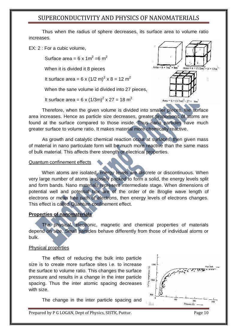
EX: 2 : For a cubic volume,
Surface area = 6 x 1m2 =6 m2
When it is divided it 8 pieces
It surface area = 6 x (1/2 m)2 x 8 = 12 m2
When the sane volume id divided into 27 pieces,
It surface area = 6 x (1/3m)2 x 27 = 18 m2
Therefore, when the given volume is divided into smaller pieces, the surface
area increases. Hence as particle size decreases, greater proportions of atoms are
found at the surface compared to those inside. Thus nano particles have much
greater surface to volume ratio. It makes material more chemically reactive.
As growth and catalytic chemical reaction occur at surfaces, then given mass
of material in nano particulate form will be much more reactive than the same mass
of bulk material. This affects there strength or electrical properties.
Quantum confinement effects
When atoms are isolated, energy levels are discrete or discontinuous. When
very large number of atoms is closely packed to form a solid, the energy levels split
and form bands. Nano materials represent intermediate stage. When dimensions of
potential well and potential box are of the order of de Broglie wave length of
electrons or mean free path of electrons, then energy levels of electrons changes.
This effect is called Quantum confinement effect.
Properties of nanomaterials
The physical, electronic, magnetic and chemical properties of materials
depend on size. Small particles behave differently from those of individual atoms or
bulk.
Physical properties
The effect of reducing the bulk into particle
size is to create more surface sites i.e. to increase
the surface to volume ratio. This changes the surface
pressure and results in a change in the inter particle
spacing. Thus the inter atomic spacing decreases
with size.
The change in the inter particle spacing and
SUPERCONDUCTIVITY AND PHYSICS OF NANOMATERIALS
Prepared by P G LOGAN, Dept of Physics, SISTK, Puttur. Page 11
the large surface to volume ratio in particle have a combined effect on material
properties. Variation in the surface free energy changes the chemical potential. This
affects the thermodynamic properties like melting point. The melting point decreases
with size and at very small sizes the decrease is faster.
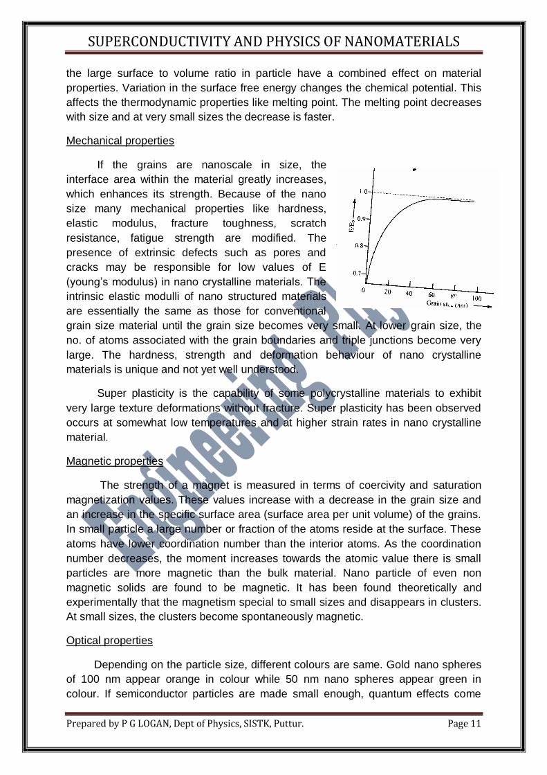
Mechanical properties
If the grains are nanoscale in size, the
interface area within the material greatly increases,
which enhances its strength. Because of the nano
size many mechanical properties like hardness,
elastic modulus, fracture toughness, scratch
resistance, fatigue strength are modified. The
presence of extrinsic defects such as pores and
cracks may be responsible for low values of E
(young‟s modulus) in nano crystalline materials. The
intrinsic elastic modulli of nano structured materials
are essentially the same as those for conventional
grain size material until the grain size becomes very small. At lower grain size, the
no. of atoms associated with the grain boundaries and triple junctions become very
large. The hardness, strength and deformation behaviour of nano crystalline
materials is unique and not yet well understood.
Super plasticity is the capability of some polycrystalline materials to exhibit
very large texture deformations without fracture. Super plasticity has been observed
occurs at somewhat low temperatures and at higher strain rates in nano crystalline
material.
Magnetic properties
The strength of a magnet is measured in terms of coercivity and saturation
magnetization values. These values increase with a decrease in the grain size and
an increase in the specific surface area (surface area per unit volume) of the grains.
In small particle a large number or fraction of the atoms reside at the surface. These
atoms have lower coordination number than the interior atoms. As the coordination
number decreases, the moment increases towards the atomic value there is small
particles are more magnetic than the bulk material. Nano particle of even non
magnetic solids are found to be magnetic. It has been found theoretically and
experimentally that the magnetism special to small sizes and disappears in clusters.
At small sizes, the clusters become spontaneously magnetic.
Optical properties
Depending on the particle size, different colours are same. Gold nano spheres
of 100 nm appear orange in colour while 50 nm nano spheres appear green in
colour. If semiconductor particles are made small enough, quantum effects come
SUPERCONDUCTIVITY AND PHYSICS OF NANOMATERIALS
Prepared by P G LOGAN, Dept of Physics, SISTK, Puttur. Page 12
into play, which limits the energies at which electrons and holes can exist in the
particles. As energy is related to wavelength or colour, the optical properties of the
particles can be finely tuned depending on its size. Thus particles can be made to
emit or absorb specific wavelength of light, merely by controlling their size.
An electro chromic device consist of materials in which an optical absorption
band can be introduced or existing band can be altered by the passage of current
through the materials, or by the application of an electric field. They are similar to
liquid crystal displays (LCD) commonly used in calculator and watches. The
resolution, brightness and contrast of these devices depend on tungstic acid gel‟s
grain size.
Thermal properties
Increasing the number of grain boundaries will enhance phonon scattering at
the disordered boundaries, resulting in lower thermal conductivity. Thus,
nanocrystalline materials would be expected to have lower thermal conductivity
compared to conventional materials. However, as the grain sizes assume
nanodimensions, their size becomes comparable to the mean free paths of phonons
that transport thermal energy. Thus, nanomaterials can show widely different
properties compared to coarse-grained materials, due to the photon confinement and
quantisation effects of photon transport. It has been observed that in addition to the
grain size, the shape also has an influence on the thermal properties of
nanomaterials.
Synthesis of nanomaterials
There are two main processes used for the synthesis of nanomaterials.
Ball milling Electrodeposition
Plasma arching Solution phase reducation
Laser sputtering Sol-gel method
Vapour deposition method Colloidal method
Ball milling
In this method, small balls are allowed to rotate around the inside of a drum and
then fall on a solid with gravity force and crush the solid into nanocrystallites. Ball
milling can be used to prepare a wide range of elemental and oxide powders. Ball
milling is the preferred method for preparing metal oxides.
Synthesis of nanomaterials
Top-down Bottom-up
SUPERCONDUCTIVITY AND PHYSICS OF NANOMATERIALS
Prepared by P G LOGAN, Dept of Physics, SISTK, Puttur. Page 13
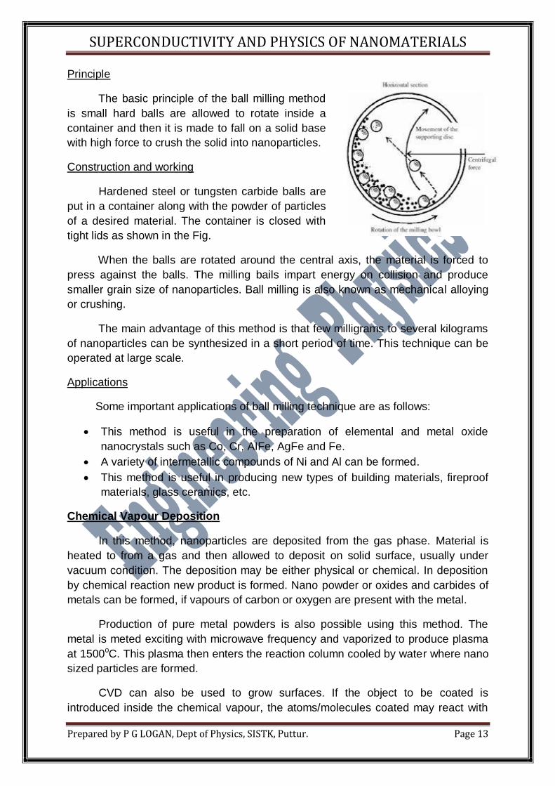
Principle
The basic principle of the ball milling method
is small hard balls are allowed to rotate inside a
container and then it is made to fall on a solid base
with high force to crush the solid into nanoparticles.
Construction and working
Hardened steel or tungsten carbide balls are
put in a container along with the powder of particles
of a desired material. The container is closed with
tight lids as shown in the Fig.
When the balls are rotated around the central axis, the material is forced to
press against the balls. The milling bails impart energy on collision and produce
smaller grain size of nanoparticles. Ball milling is also known as mechanical alloying
or crushing.
The main advantage of this method is that few milligrams to several kilograms
of nanoparticles can be synthesized in a short period of time. This technique can be
operated at large scale.
Applications
Some important applications of ball milling technique are as follows:
This method is useful in the preparation of elemental and metal oxide
nanocrystals such as Co, Cr, AIFe, AgFe and Fe.
A variety of intermetallic compounds of Ni and Al can be formed.
This method is useful in producing new types of building materials, fireproof
materials, glass ceramics, etc.
Chemical Vapour Deposition
In this method, nanoparticles are deposited from the gas phase. Material is
heated to from a gas and then allowed to deposit on solid surface, usually under
vacuum condition. The deposition may be either physical or chemical. In deposition
by chemical reaction new product is formed. Nano powder or oxides and carbides of
metals can be formed, if vapours of carbon or oxygen are present with the metal.
Production of pure metal powders is also possible using this method. The
metal is meted exciting with microwave frequency and vaporized to produce plasma
at 1500oC. This plasma then enters the reaction column cooled by water where nano
sized particles are formed.
CVD can also be used to grow surfaces. If the object to be coated is
introduced inside the chemical vapour, the atoms/molecules coated may react with
SUPERCONDUCTIVITY AND PHYSICS OF NANOMATERIALS
Prepared by P G LOGAN, Dept of Physics, SISTK, Puttur. Page 14
the substrate atoms/molecules. The way the atoms /molecules grow on the surface
of the substrate depends on the alignment of the atoms /molecules of the substrate.
Surfaces with unique characteristics can be grown with these techniques.
Sol – Gel
Sol :: A material which when reacts with liquid converts in to a gelly or viscous fluid.
Colloid :: A substance which converts liquid to semisolid or viscous or cloudy.
Gel :: Amore thicky substance.
Soot :: When a compound is brunt, it given black fumes called soot.
In solutions molecules of nanometer size are
dispersed and move around randomly and hence
the solutions are clear. In colloids, the molecules of
size ranging from 20μm to100μm are suspended in
a solvent. When mixed with a liquid colloids look
cloudy or even milky. A colloid that is suspended in
a liquid is called as sol. A suspension that keeps its
shape is called a gel. Thus sol-gels are
suspensions of colloids in liquids that keep their
shape.
Sol - gel formation occurs in different stages.
1) Hydrolysis
2) Condensation and polymerization of monomers to form particles
3) Agglomeration of particles. This is followed by formation of networks which
extends throughout the liquid medium and forms a gel.
The rate of hydrolysis and condensation reactions are governed by various
factors such as PH, temperature, H2O/Si molar ratio, nature and concentration of
catalyst and process of drying. Under proper conditions spherical nanoparticles are
produced.
Plasma arching
Plasma is an ionized gas. To produce plasma, potential difference is applied
across two electrodes. The gas yields up its electrons and gets ionized .Ionized gas
(plasma) conducts electricity. A plasma arcing device consists of two electrodes. An
arc passes from one electrode to the other. From the anode electrode due to the
potential difference electrons are emitted. Positively charged ions pass to the other
electrode (cathode), pick up the electron and are deposited to form nanoparticles. As
a surface deposit the depth of the coating must be only a few atoms. Each particle

SUPERCONDUCTIVITY AND PHYSICS OF NANOMATERIALS
Prepared by P G LOGAN, Dept of Physics, SISTK, Puttur. Page 15
must be nanosized and independent. The interaction among them must be by
hydrogen bonding or Vander Waals forces. Plasma arcing is used to produced
carbon nanotubes.
Thermal Evaporation
Thermal evaporation often uses a filament of high current passing through it,
producing sufficient amount of thermal energy, which heats up the material to be
deposited. When the substance is heated adequately, it begins to evaporate and
travel through the chamber and deposit on the substrate to be coated. The higher
the vacuum, the more athriiiefficiently material will be deposited to the substrate. In a
higher vacuum, there are less number of molecules in the chamber, which will
increase the 'mean free path' and a longer mean free path will allow the evaporated
molecules to travel further before striking an unwanted molecule in the chamber. The
rate of deposition can be controlled by the current being passed through the filament.
CARBON NANOTUBES (CNT’S)
We know three forms of carbon
namely diamond graphite and
amorphous carbon. There is a whole
family of other forms of carbon known
as carbon nanotubes, which are
related to graphite. In conventional
graphite, the sheets of carbon are
stacked on top of one another .They
can easily slide over each other. That‟s
why graphite is not hard and can be used as a lubricant. When graphite sheets are
rolled into a cylinder and their edges joined, they form carbon nanotubes i.e. carbon
nanotubes are extended tubes of rolled graphite sheets. Generally, the carbon
nanotubes are formed in the range of 2 to 10 nm in diameter and a length of 100 µm.
Carbon nanotubes are classified into single wall carbon nanotube (SWCNT)
and Multiwall Carbon nanotube (MWCNT) depending upon the walls contained by
them.
Properties
Carbon nanotubes are the strongest and stiffest material in terms of tensile
strengths and elastic modulus respectively.
Multiwall carbon nanotube exhibit telescoping property whereby an inner
nanotube core slide without friction with in its outer nanotube shell creating an
atomically perfect linear or molecular bearing.
Because of the symmetry and unique electronic structure of graphene, CNT
will act as metallic as well as a semiconductor.
SUPERCONDUCTIVITY AND PHYSICS OF NANOMATERIALS
Prepared by P G LOGAN, Dept of Physics, SISTK, Puttur. Page 16
Semiconducting CNT exhibits high carrier mobilities which inturn exhibit high
current density.
All CNTS are good thermal conductors.
CNTs exhibits optical activity and hence they are used in optical devices.
They exhibits enhanced chemical reactivity.
CNT exhibit magneto resistance phenomena.
High Strength Applications
The CNT are very strong, that is, they are about 10 times stronger than steel.
Let us consider that one end of a thin wire is nailed to the roof of a room while a
weight W is attached to the other end. The stress acting on the wire is given by
S=W/A where A is the cross-sectional area of the wire.
The strain of the wire is given by the amount of stretch ∆L of the wire of length
L, S =∆L/L where L is the length of the wire before attaching the weight.
We known that stress is proportional to strain S=Ee
where E is the proportionality constant and is equal to LW/A ∆L, known as Young's
modulus.
The Young's modulus of the material is used to characterise the elastic
flexibility. For example, the larger the value of Young's modulus the lesser is the
flexibility. The Young's modulus of the carbon nanotube is in the range from 1.28 to
1.8 Tpa (1 Tpa 107 atm), while for steel, it is 0.21 Tpa. It means that the CNT is 10
times stronger than that of steel. This property of SWCNT and MWCNT makes the
nanotubes a different material from other conventional materials which finds wide
variety of high strength applications.
Graphene
Graphene is a one-atom-thick planar
sheet of sp2-bonded carbon atoms that are
densely packed in a honeycomb crystal
lattice. The name comes from GRAPHITE + -
ENE; graphite itself consists of many
graphene sheets stacked together. The
carbon-carbon bond length in graphene is
approximately 1.42 Å. Graphene is the basic
structural element of all other graphitic
materials including graphite, carbon
nanotubes and fullerenes. It can also be considered as an infinitely large aromatic
molecule, the limiting case of the family of flat polycyclic aromatic hydrocarbons
called graphenes.
SUPERCONDUCTIVITY AND PHYSICS OF NANOMATERIALS
Prepared by P G LOGAN, Dept of Physics, SISTK, Puttur. Page 17
Properties
The expected structure of graphene is hexagonal lattice.
Intrinsic graphene is a semi-metal or zero-gap semiconductor.
It exhibits high electron mobility at room temperature.
It is an ideal material for spintronics due to small spin orbit interaction and
near absence of nuclear magnetic moments in carbon.
It exhibits anomalous quantum hall effect.
It exhibit high opacity.
It exhibit high thermal conductivity at room temperature.
It exhibit high Young's modulus hence it is very strong and rigid.
It exhibit high carrier mobility hence it is used as the channel in a FET.
Graphene-Based FET
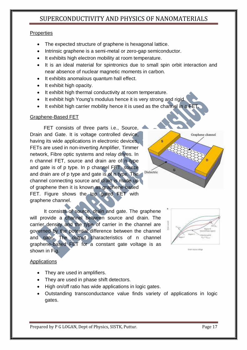
FET consists of three parts i.e., Source,
Drain and Gate. It is voltage controlled device,
having its wide applications in electronic devices.
FETs are used in non-inverting Amplifier, Timmer
network, Fibre optic systems and relay drives. In
n channel FET, source and drain are of n type
and gate is of p type. In p channel FET, source
and drain are of p type and gate is of n type. The
channel connecting source and drain is made up
of graphene then it is known as graphene-based
FET. Figure shows the top gated FET with
graphene channel.
It consists of source, drain and gate. The graphene
will provide a channel between source and drain. The
carrier density and the type of carrier in the channel are
governed by the potential difference between the channel
and gate. The output characteristics of n channel
graphene-based FET for a constant gate voltage is as
shown in Fig.
Applications
They are used in amplifiers.
They are used in phase shift detectors.
High on/off ratio has wide applications in logic gates.
Outstanding transconductance value finds variety of applications in logic
gates.
SUPERCONDUCTIVITY AND PHYSICS OF NANOMATERIALS
Prepared by P G LOGAN, Dept of Physics, SISTK, Puttur. Page 18
Application of Nanomaterials
Material Technology
• Nanocrystalline aerogel are light in weight and since they are porous, air is
trapped at the interstices. Aerogels are used for insulation in offices, homes,
etc.
• Cutting tools made of Nanocrystalline materials are much harder, much more
wear-resistant, and- last longer.
• Sensors made from Nanocrystalline materials are sensitive to changes in their
environment. Thus, they are used for smoke detectors, ice detectors on
aircraft wings, etc.
• Nanocrystalline materials are used for high energy-density batteries.
• Nanoengineered membranes could potentially lead to more energy efficient-
water-purification processes.
• Nanosized titanium dioxide and zinc oxide are used in sunscreens to absorb
and reflect ultraviolet rays.
Information Technology
• Nanoscale-fabricated magnetic materials are used in data storage.
• Nano computer chips reduce the size of the microprocessor with
nanocrystalline starting materials, ultra-high purity materials with better
thermal conductivity and durable interconnections.
• Nanocrystalline light-emitting phosphors are used for flat panel displays.
• Nanoparticles are used for information storage.
• Nanophotonic crystals are used in chemical optical computers.
• Nano thickness-controlled coating are used in optoelectronic devices.
Biomedicals
• Nanocrystalline silicon carbide is used for artificial heart valves due to its low
weight, high strength and inertness.
• Biosensitive nanomaterials are used for tagging of DNA and DNA chips.
• In the medical field, nanomaterials are used for disease diagnosis, drug
delivery and molecular imaging.
• Nanostructured ceramics readily interact with bone cells and hence are used
as implant material.
Energy Storage
• Addition of nanoparticles to diesel fuel improves fuel economy by reducing the
degradation of fuel consumption.
• Nanoparticles are used in hydrogen-storage devices.
• Nanoparticles are used in magnetic refrigeration.
• Metal nanoparticles are useful in fabrication of ionic batteries.
![Superconductivity and its applications - UNIGEGroup of Applied Superconductivity Department of Quantum Matter Physics University of Geneva, Switzerland Bi2212 Bi2223 a [Å] 5.415 5.413](https://img.pdfslide.us/doc/110x75/5ec86f12997044603330eacb/superconductivity-and-its-applications-unige-group-of-applied-superconductivity.jpg)