Embed Size (px)
Citation preview
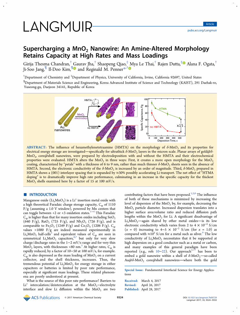
Supercharging a MnO2 Nanowire: An Amine-Altered MorphologyRetains Capacity at High Rates and Mass LoadingsGirija Thesma Chandran,† Gaurav Jha,† Shaopeng Qiao,‡ Mya Le Thai,† Rajen Dutta,‡ Alana F. Ogata,†
Ji-Soo Jang,¶ Il-Doo Kim,¶ and Reginald M. Penner*,†
†Department of Chemistry and ‡Department of Physics, University of California, Irvine, California 92697, United States¶Department of Materials Science and Engineering, Korea Advanced Institute of Science and Technology (KAIST), 291 Daehak-ro,Yuseong-gu, Daejeon 34141, Republic of Korea
ABSTRACT: The influence of hexamethylenetetraamine (HMTA) on the morphology of δ-MnO2 and its properties forelectrical energy storage are investigatedspecifically for ultrathick δ-MnO2 layers in the micron scale. Planar arrays of gold@δ-MnO2, core@shell nanowires, were prepared by electrodeposition with and without the HMTA and their electrochemicalproperties were evaluated. HMTA alters the MnO2 in three ways: First, it creates a more open morphology for the MnO2coating, characterized by “petals” with a thickness of 6 to 9 nm, rather than much thinner δ-MnO2 sheets seen in the absence ofHMTA. Second, the electronic conductivity of the δ-MnO2 is increased by an order of magnitude. Third, δ-MnO2 prepared inHMTA shows a (001) interlayer spacing that is expanded by ≈30% possibly accelerating Li transport. The net effect of “HTMAdoping” is to dramatically improve high rate performance, culminating in an increase in the specific capacity for the thickestMnO2 shells examined here by a factor of 15 at 100 mV/s.
■ INTRODUCTIONManganese oxide (LixMnO2) is a Li
+ insertion metal oxide witha high theoretical Faradaic charge storage capacity, Csp of 1110F/g (assuming a 1.0 V window), powered by Mn centers thatcan toggle between +2 or +3 oxidation states.1−4 This FaradaicCsp is higher than that for many insertion oxides including SnO2(640 F/g), RuO2 (725 F/g), and Nb2O5 (726 F/g), and iscomparable to Fe2O3 (1249 F/g) and Co3O4 (1206 F/g). Cspvalues >1000 F/g are indeed measured experimentally inLixMnO2 half-cells5 and equivalent values of Csp are seen insymmetrical LixMnO2 capacitors,6,7 but only for very slowcharge/discharge rates in the 1−2 mV/s range and for very thinMnO2 layers, with thicknesses <80 nm.5 At higher rates, Csp israpidly reduced, by a factor of 10−50 at 100 mV/s, for example.Csp is also depressed as the mass loading of MnO2 on a currentcollector, and the shell thickness, increases. Thus, thetremendous potential of LixMnO2 for energy storage in eithercapacitors or batteries is limited by poor rate performance,especially at significant mass loadings. These related phenom-ena are poorly understood at present.What is the source of this poor rate performance? Barriers to
Li+ intercalation/deintercalation at the MnO2−electrolyteinterface and slow Li diffusion within the MnO2 are two
contributing factors that have been proposed.1,3,8 The influenceof both of these mechanisms is minimized by increasing thelevel of dispersion of the MnO2 by, for example, decreasing theMnO2 particle diameter. Increased dispersion translates into ahigher surface area:volume ratio and reduced diffusion pathlengths within the MnO2 for Li. A significant disadvantage ofLixMnO2again shared by other metal oxidesis its lowelectronic conductivity which varies from 2 to 4 × 10⁻⁴ S/cm(x = 0) increasing to 4−5 × 10⁻² S/cm (for x = 1.0) ascompared with ≈105 S/cm for a metal such as silver.9 The lowconductivity of LixMnO2 necessitates that it be supported athigh dispersion on a good conductor such as a metal or carbon,and many examples of this general paradigm have beenreported (e.g., refs 10−22). Our approach5−7 has been toembed a gold nanowire within a shell of δ-MnO2so-calledAu@δ-MnO2 core@shell nanowireswhere both the gold
Special Issue: Fundamental Interfacial Science for Energy Applica-tions
Received: March 4, 2017Revised: April 26, 2017Published: April 28, 2017
Article
pubs.acs.org/Langmuir
© 2017 American Chemical Society 9324 DOI: 10.1021/acs.langmuir.7b00729Langmuir 2017, 33, 9324−9332
nanowires and the δ-MnO2 shell are prepared by electro-deposition. A key point is that the gold nanowire core does notensure facile electrical communication with the MnO2 shellwhen this shell increases in thickness beyond 60 nm or so. InAu@MnO2 nanowires, the MnO2 shell must still intercalate Li+
and communicate electrically with the gold nanowire core, andthe strategy outlined here is intended to impact one or both ofthese processes.The well-known limitations of MnO2 have stimulated
interest in improving it, as already indicated. Hundreds ofpapers already describe the mitigation of the low electronicconductivity of MnO2 by the preparation of composites ofMnO2 with graphene,10−14 carbon nanotubes,15−19 conductivepolymers,20−22 and other electrically conductive materials. Inaddition to the preparation of composites, there is some workaimed at altering the properties of the MnO2 itself. Chen andco-workers23 evaporated gold into MnO2 films, therebyincreasing the half-cell Csp by a factor of 2 at 100 mV/s. Thisincrease was attributed to the increased electrical conductivityof the MnO2/Au composite. The MnO2 morphology has beenaltered by hydrothermal synthesis in the presence of asurfactant, poly(vinylpyrrolidone) (PVP).24 Single 40−50 nmdiameter nanowires of MnO2 with micron-scale lengthsprepared by this technique showed a higher Csp as comparedwith larger nanorods.24 Nakayama and co-workers25−27
prepared electrodeposited birnessite MnO2 incorporating avariety of dopants including poly(diallyldimethyl-ammonium)cations,25 methyl viologen,26 and long chain, n-alkyl ammoniumcations.27 The d-spacing of the birnessite was adjusted overseveral nanometers by these dopant species, and applications ofthese composite materials to the catalysis of the oxygenevolution reaction were explored.28
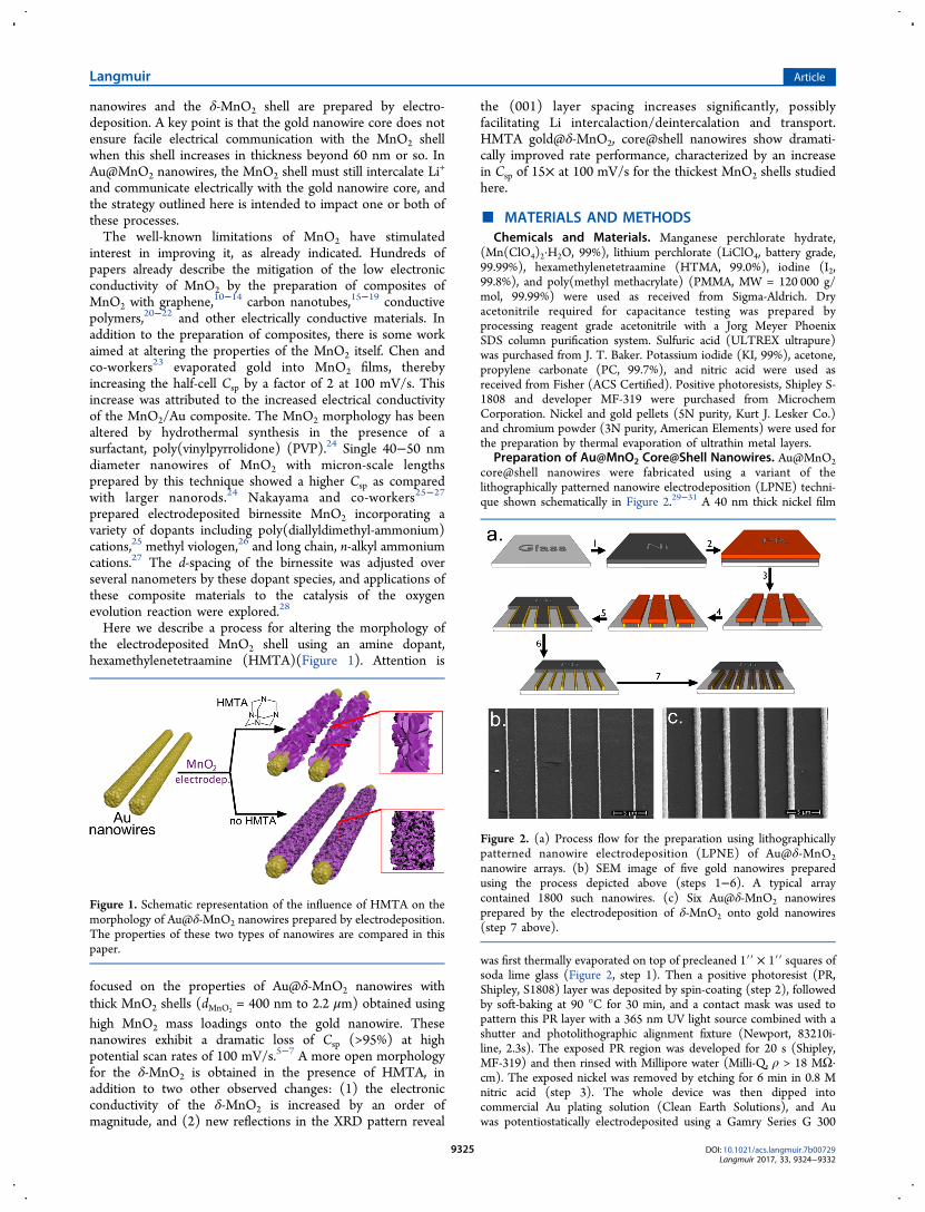
Here we describe a process for altering the morphology ofthe electrodeposited MnO2 shell using an amine dopant,hexamethylenetetraamine (HMTA)(Figure 1). Attention is
focused on the properties of Au@δ-MnO2 nanowires withthick MnO2 shells (dMnO2
= 400 nm to 2.2 μm) obtained usinghigh MnO2 mass loadings onto the gold nanowire. Thesenanowires exhibit a dramatic loss of Csp (>95%) at highpotential scan rates of 100 mV/s.5−7 A more open morphologyfor the δ-MnO2 is obtained in the presence of HMTA, inaddition to two other observed changes: (1) the electronicconductivity of the δ-MnO2 is increased by an order ofmagnitude, and (2) new reflections in the XRD pattern reveal
the (001) layer spacing increases significantly, possiblyfacilitating Li intercalaction/deintercalation and transport.HMTA gold@δ-MnO2, core@shell nanowires show dramati-cally improved rate performance, characterized by an increasein Csp of 15× at 100 mV/s for the thickest MnO2 shells studiedhere.
■ MATERIALS AND METHODSChemicals and Materials. Manganese perchlorate hydrate,
(Mn(ClO4)2·H2O, 99%), lithium perchlorate (LiClO4, battery grade,99.99%), hexamethylenetetraamine (HTMA, 99.0%), iodine (I2,99.8%), and poly(methyl methacrylate) (PMMA, MW = 120 000 g/mol, 99.99%) were used as received from Sigma-Aldrich. Dryacetonitrile required for capacitance testing was prepared byprocessing reagent grade acetonitrile with a Jorg Meyer PhoenixSDS column purification system. Sulfuric acid (ULTREX ultrapure)was purchased from J. T. Baker. Potassium iodide (KI, 99%), acetone,propylene carbonate (PC, 99.7%), and nitric acid were used asreceived from Fisher (ACS Certified). Positive photoresists, Shipley S-1808 and developer MF-319 were purchased from MicrochemCorporation. Nickel and gold pellets (5N purity, Kurt J. Lesker Co.)and chromium powder (3N purity, American Elements) were used forthe preparation by thermal evaporation of ultrathin metal layers.
Preparation of Au@MnO2 Core@Shell Nanowires. Au@MnO2core@shell nanowires were fabricated using a variant of thelithographically patterned nanowire electrodeposition (LPNE) techni-que shown schematically in Figure 2.29−31 A 40 nm thick nickel film
was first thermally evaporated on top of precleaned 1′′ × 1′′ squares ofsoda lime glass (Figure 2, step 1). Then a positive photoresist (PR,Shipley, S1808) layer was deposited by spin-coating (step 2), followedby soft-baking at 90 °C for 30 min, and a contact mask was used topattern this PR layer with a 365 nm UV light source combined with ashutter and photolithographic alignment fixture (Newport, 83210i-line, 2.3s). The exposed PR region was developed for 20 s (Shipley,MF-319) and then rinsed with Millipore water (Milli-Q, ρ > 18 MΩ·cm). The exposed nickel was removed by etching for 6 min in 0.8 Mnitric acid (step 3). The whole device was then dipped intocommercial Au plating solution (Clean Earth Solutions), and Auwas potentiostatically electrodeposited using a Gamry Series G 300
Figure 1. Schematic representation of the influence of HMTA on themorphology of Au@δ-MnO2 nanowires prepared by electrodeposition.The properties of these two types of nanowires are compared in thispaper.
Figure 2. (a) Process flow for the preparation using lithographicallypatterned nanowire electrodeposition (LPNE) of Au@δ-MnO2nanowire arrays. (b) SEM image of five gold nanowires preparedusing the process depicted above (steps 1−6). A typical arraycontained 1800 such nanowires. (c) Six Au@δ-MnO2 nanowiresprepared by the electrodeposition of δ-MnO2 onto gold nanowires(step 7 above).
Langmuir Article
DOI: 10.1021/acs.langmuir.7b00729Langmuir 2017, 33, 9324−9332
9325
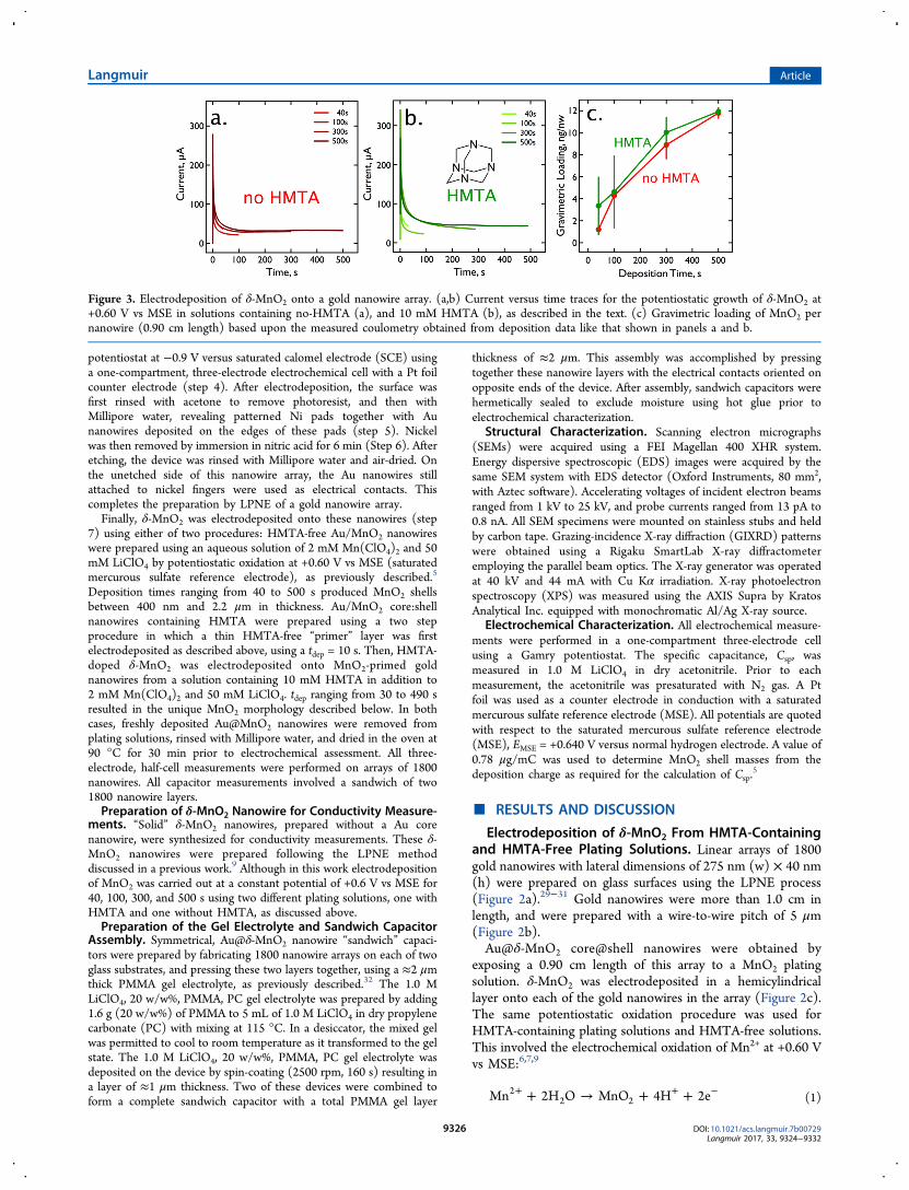
potentiostat at −0.9 V versus saturated calomel electrode (SCE) usinga one-compartment, three-electrode electrochemical cell with a Pt foilcounter electrode (step 4). After electrodeposition, the surface wasfirst rinsed with acetone to remove photoresist, and then withMillipore water, revealing patterned Ni pads together with Aunanowires deposited on the edges of these pads (step 5). Nickelwas then removed by immersion in nitric acid for 6 min (Step 6). Afteretching, the device was rinsed with Millipore water and air-dried. Onthe unetched side of this nanowire array, the Au nanowires stillattached to nickel fingers were used as electrical contacts. Thiscompletes the preparation by LPNE of a gold nanowire array.Finally, δ-MnO2 was electrodeposited onto these nanowires (step
7) using either of two procedures: HMTA-free Au/MnO2 nanowireswere prepared using an aqueous solution of 2 mM Mn(ClO4)2 and 50mM LiClO4 by potentiostatic oxidation at +0.60 V vs MSE (saturatedmercurous sulfate reference electrode), as previously described.5
Deposition times ranging from 40 to 500 s produced MnO2 shellsbetween 400 nm and 2.2 μm in thickness. Au/MnO2 core:shellnanowires containing HMTA were prepared using a two stepprocedure in which a thin HMTA-free “primer” layer was firstelectrodeposited as described above, using a tdep = 10 s. Then, HMTA-doped δ-MnO2 was electrodeposited onto MnO2-primed goldnanowires from a solution containing 10 mM HMTA in addition to2 mM Mn(ClO4)2 and 50 mM LiClO4. tdep ranging from 30 to 490 sresulted in the unique MnO2 morphology described below. In bothcases, freshly deposited Au@MnO2 nanowires were removed fromplating solutions, rinsed with Millipore water, and dried in the oven at90 °C for 30 min prior to electrochemical assessment. All three-electrode, half-cell measurements were performed on arrays of 1800nanowires. All capacitor measurements involved a sandwich of two1800 nanowire layers.Preparation of δ-MnO2 Nanowire for Conductivity Measure-
ments. “Solid” δ-MnO2 nanowires, prepared without a Au corenanowire, were synthesized for conductivity measurements. These δ-MnO2 nanowires were prepared following the LPNE methoddiscussed in a previous work.9 Although in this work electrodepositionof MnO2 was carried out at a constant potential of +0.6 V vs MSE for40, 100, 300, and 500 s using two different plating solutions, one withHMTA and one without HMTA, as discussed above.Preparation of the Gel Electrolyte and Sandwich Capacitor
Assembly. Symmetrical, Au@δ-MnO2 nanowire “sandwich” capaci-tors were prepared by fabricating 1800 nanowire arrays on each of twoglass substrates, and pressing these two layers together, using a ≈2 μmthick PMMA gel electrolyte, as previously described.32 The 1.0 MLiClO4, 20 w/w%, PMMA, PC gel electrolyte was prepared by adding1.6 g (20 w/w%) of PMMA to 5 mL of 1.0 M LiClO4 in dry propylenecarbonate (PC) with mixing at 115 °C. In a desiccator, the mixed gelwas permitted to cool to room temperature as it transformed to the gelstate. The 1.0 M LiClO4, 20 w/w%, PMMA, PC gel electrolyte wasdeposited on the device by spin-coating (2500 rpm, 160 s) resulting ina layer of ≈1 μm thickness. Two of these devices were combined toform a complete sandwich capacitor with a total PMMA gel layer
thickness of ≈2 μm. This assembly was accomplished by pressingtogether these nanowire layers with the electrical contacts oriented onopposite ends of the device. After assembly, sandwich capacitors werehermetically sealed to exclude moisture using hot glue prior toelectrochemical characterization.
Structural Characterization. Scanning electron micrographs(SEMs) were acquired using a FEI Magellan 400 XHR system.Energy dispersive spectroscopic (EDS) images were acquired by thesame SEM system with EDS detector (Oxford Instruments, 80 mm2,with Aztec software). Accelerating voltages of incident electron beamsranged from 1 kV to 25 kV, and probe currents ranged from 13 pA to0.8 nA. All SEM specimens were mounted on stainless stubs and heldby carbon tape. Grazing-incidence X-ray diffraction (GIXRD) patternswere obtained using a Rigaku SmartLab X-ray diffractometeremploying the parallel beam optics. The X-ray generator was operatedat 40 kV and 44 mA with Cu Kα irradiation. X-ray photoelectronspectroscopy (XPS) was measured using the AXIS Supra by KratosAnalytical Inc. equipped with monochromatic Al/Ag X-ray source.
Electrochemical Characterization. All electrochemical measure-ments were performed in a one-compartment three-electrode cellusing a Gamry potentiostat. The specific capacitance, Csp, wasmeasured in 1.0 M LiClO4 in dry acetonitrile. Prior to eachmeasurement, the acetonitrile was presaturated with N2 gas. A Ptfoil was used as a counter electrode in conduction with a saturatedmercurous sulfate reference electrode (MSE). All potentials are quotedwith respect to the saturated mercurous sulfate reference electrode(MSE), EMSE = +0.640 V versus normal hydrogen electrode. A value of0.78 μg/mC was used to determine MnO2 shell masses from thedeposition charge as required for the calculation of Csp.
5
■ RESULTS AND DISCUSSION
Electrodeposition of δ-MnO2 From HMTA-Containingand HMTA-Free Plating Solutions. Linear arrays of 1800gold nanowires with lateral dimensions of 275 nm (w) × 40 nm(h) were prepared on glass surfaces using the LPNE process(Figure 2a).29−31 Gold nanowires were more than 1.0 cm inlength, and were prepared with a wire-to-wire pitch of 5 μm(Figure 2b).Au@δ-MnO2 core@shell nanowires were obtained by
exposing a 0.90 cm length of this array to a MnO2 platingsolution. δ-MnO2 was electrodeposited in a hemicylindricallayer onto each of the gold nanowires in the array (Figure 2c).The same potentiostatic oxidation procedure was used forHMTA-containing plating solutions and HMTA-free solutions.This involved the electrochemical oxidation of Mn2+ at +0.60 Vvs MSE:6,7,9
+ → + ++ + −Mn 2H O MnO 4H 2e22 2 (1)
Figure 3. Electrodeposition of δ-MnO2 onto a gold nanowire array. (a,b) Current versus time traces for the potentiostatic growth of δ-MnO2 at+0.60 V vs MSE in solutions containing no-HMTA (a), and 10 mM HMTA (b), as described in the text. (c) Gravimetric loading of MnO2 pernanowire (0.90 cm length) based upon the measured coulometry obtained from deposition data like that shown in panels a and b.
Langmuir Article
DOI: 10.1021/acs.langmuir.7b00729Langmuir 2017, 33, 9324−9332
9326
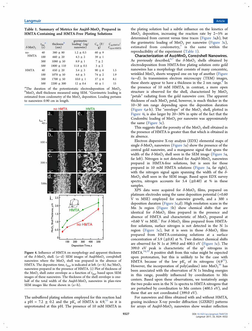
The unbuffered plating solution employed for this reaction hada pH = 7.2 ± 0.2 and the pKa of HMTA is 4.9,33 so it isunprotonated at this pH. The presence of 10 mM HMTA in
the plating solution had a subtle influence on the kinetics ofMnO2 deposition, increasing the reaction rate by 2−5% asdetermined from current versus time traces (Figure 3a,b), butthe gravimetric loading of MnO2 per nanowire (Figure 3c),estimated from coulometry,5 is the same within thereproducibility of the experiment (Table 1).
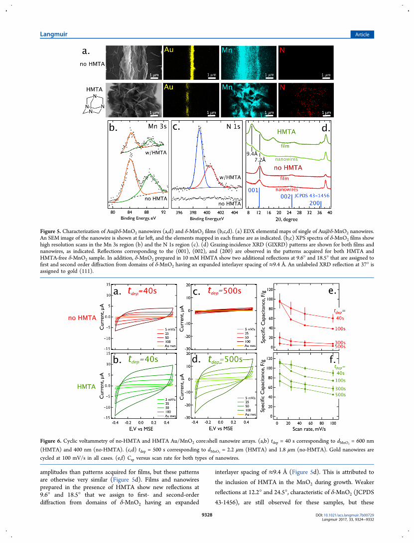
Characterization of Au@MnO2 Core@shell Nanowires.As previously described,6,7 the δ-MnO2 shells obtained byelectrodeposition from HMTA-free plating solution onto goldnanowires has a morphology that consists of many concentric,wrinkled MnO2 sheets wrapped one on top of another (Figure4a−d). In transmission electron microscopy (TEM) images,these sheets appear to have a thickness in the 2 nm range.6 Inthe presence of 10 mM HMTA, in contrast, a more openstructure is observed for the shell, characterized by MnO2“petals” radiating from the gold nanowire core. The apparentthickness of each MnO2 petal, however, is much thicker in the10−30 nm range depending upon the deposition duration(Figure 4,e-h). The “envelope” of the MnO2 shell, plotted inFigure 4i, is also larger by 20−30% in spite of the fact that theCoulombic loading of MnO2 per nanowire was approximatelythe same (Figure 3c).This suggests that the porosity of the MnO2 shell obtained in
the presence of HMTA is greater than that which is obtained inits absence.Electron dispersive X-ray analysis (EDX) elemental maps of
single δ-MnO2 nanowires (Figure 5a) show the presence of thecentral gold nanowire, and a manganese signal that spans thewidth of the δ-MnO2 shell seen in the SEM image (Figure 5a,far left). Nitrogen is not detected for Au@δ-MnO2 nanowiresprepared in HMTA-free solutions, but is seen for thoseprepared in 10 mM HMTA solutions (Figure 5a, far right),with the nitrogen signal again spanning the width of the δ-MnO2 shell seen in the SEM image. Based upon EDX surveyspectra, nitrogen accounts for 5.4 (±0.40) at % in thesesamples.XPS data were acquired for δ-MnO2 films, prepared on
platinum electrodes using the same deposition potential (+0.60V vs MSE) employed for nanowire growth, and a 300 sdeposition duration (Figure 5c,d). High resolution scans in theMn 3s region (Figure 5b) show chemical shifts that areidentical for δ-MnO2 films prepared in the presence andabsence of HMTA and characteristic of MnO2 prepared at+0.60 V vs MSE.7 For δ-MnO2 films prepared from HMTA-free solutions, surface nitrogen is not detected in the N 1sregion (Figure 5c), but it is seen in those δ-MnO2 filmsprepared from HMTA-containing solutions at a surfaceconcentration of 5.9 (±0.8) at %. Two distinct chemical shiftsare observed for N 1s at 399.0 and 400.5 eV (Figure 5c). The399.0 eV peak is characteristic of the sp3 nitrogens inHMTA.34,35 A positive shift from this value might be expectedupon protonation, but this is unlikely to be the case withHMTA because of the low pKa of its nitrogens (4.933).However, the incorporation of poly(aniline) into MnO2
36 hasbeen associated with the observation of N 1s binding energiesin this range, possibly influenced by coordination to Mncenters. Based upon these observations, we tentatively assignthe two peaks seen in the N 1s spectra to HMTA nitrogens thatare perturbed by coordination to Mn centers (400.5 eV), andthose that are not coordinated (399.0 eV).For nanowires and films obtained with and without HMTA,
grazing incidence X-ray powder diffraction (GIXRD) patternsfor arrays of Au@δ-MnO2 nanowires show weaker reflection
Table 1. Summary of Metrics for Au@δ-MnO2 Prepared inHMTA-Containing and HMTA-Free Plating Solutions
δ-MnO2
tdepa
(s)thicknessb
(nm)
gravimetricloadingc (ng/nanowire)
Csp (F/g)
Csp,HMTA/Csp,no‑HMTA
no-HMTA
40 380 ± 80 1.2 ± 0.3 60 ± 9100 660 ± 20 4.3 ± 2 39 ± 1300 1080 ± 50 8.9 ± 1 7 ± 2500 1800 ± 110 11.8 ± 0.5 3 ± 2
HMTA 40 650 ± 20 3.4 ± 3 90 ± 6 1.5100 1070 ± 50 4.6 ± 3 74 ± 2 1.9300 1700 ± 50 10.0 ± 1 57 ± 6 8.1500 2200 ± 300 12 ± 0.4 45 ± 1 15
aThe duration of the potentiostatic electrodeposition of MnO2.bMnO2 shell thickness measured using SEM. cGravimetric loading isestimated from coulometry of the MnO2 deposition. Loading pertainsto nanowires 0.90 cm in length.
Figure 4. Influence of HMTA on morphology and apparent thicknessof the δ-MnO2 shell. (a−d) SEM images of Au@MnO2 core@shellnanowires where the MnO2 shell was prepared in the absence ofHMTA. The deposition time, tdep, is indicated at left. (e−h) Au/MnO2nanowires prepared in the presence of HMTA. (i) Plot of thickness ofthe MnO2 shell outer envelope as a function of tdep, based upon SEMimages of these nanowires. The thickness of the shell envelope is one-half of the total width of the Au@δ-MnO2 nanowires in plan-viewSEM images like those shown in (a−h).
Langmuir Article
DOI: 10.1021/acs.langmuir.7b00729Langmuir 2017, 33, 9324−9332
9327
amplitudes than patterns acquired for films, but these patternsare otherwise very similar (Figure 5d). Films and nanowiresprepared in the presence of HMTA show new reflections at9.6° and 18.5° that we assign to first- and second-orderdiffraction from domains of δ-MnO2 having an expanded
interlayer spacing of ≈9.4 Å (Figure 5d). This is attributed to
the inclusion of HMTA in the MnO2 during growth. Weaker
reflections at 12.2° and 24.5°, characteristic of δ-MnO2 (JCPDS
43-1456), are still observed for these samples, but these
Figure 5. Characterization of Au@δ-MnO2 nanowires (a,d) and δ-MnO2 films (b,c,d). (a) EDX elemental maps of single of Au@δ-MnO2 nanowires.An SEM image of the nanowire is shown at far left, and the elements mapped in each frame are as indicated. (b,c) XPS spectra of δ-MnO2 films showhigh resolution scans in the Mn 3s region (b) and the N 1s region (c). (d) Grazing-incidence XRD (GIXRD) patterns are shown for both films andnanowires, as indicated. Reflections corresponding to the (001), (002), and (200) are observed in the patterns acquired for both HMTA andHMTA-free δ-MnO2 sample. In addition, δ-MnO2 prepared in 10 mM HMTA show two additional reflections at 9.6° and 18.5° that are assigned tofirst and second order diffraction from domains of δ-MnO2 having an expanded interlayer spacing of ≈9.4 Å. An unlabeled XRD reflection at 37° isassigned to gold (111).
Figure 6. Cyclic voltammetry of no-HMTA and HMTA Au/MnO2 core:shell nanowire arrays. (a,b) tdep = 40 s corresponding to dMnO2= 600 nm
(HMTA) and 400 nm (no-HMTA). (c,d) tdep = 500 s corresponding to dMnO2= 2.2 μm (HMTA) and 1.8 μm (no-HMTA). Gold nanowires are
cycled at 100 mV/s in all cases. (e,f) Csp versus scan rate for both types of nanowires.
Langmuir Article
DOI: 10.1021/acs.langmuir.7b00729Langmuir 2017, 33, 9324−9332
9328
patterns are consistent with expansion of the interlayer spacingof δ-MnO2 by ≈30% in the presence of HMTA.The morphological, structural, and chemical changes induced
in the δ-MnO2 by HMTA, seen in the data of Figure 5, exert astrong influence on its electrochemistry particularly for verythick shells and high potential scan rates. For the thinnest shellsstudied here (tdep = 40 s) evaluated at the slowest scan rates (5mV/s), Csp is 10% higher, on average, for HMTA versus no-HMTA samples (Figure 6a,b,e). This is a modest differencethat is inside of our sample-to-sample error bars. Theconclusion is that virtually the same number of Mn centerswithin these MnO2 shells are electrochemically accessible andparticipating in Faradaic charge storage, thereby contributing toCsp. It is important to understand that the Csp = 90−110 F/gmeasured for these samples, with a shell thickness of 400−600nm (Figure 4i), is well below the theoretical value of 1110 F/g.
Csp values in this range are readily measured for arrays of Au@δ-MnO2 nanowires with much thinner shells in the 60−70 nmrange.6,7
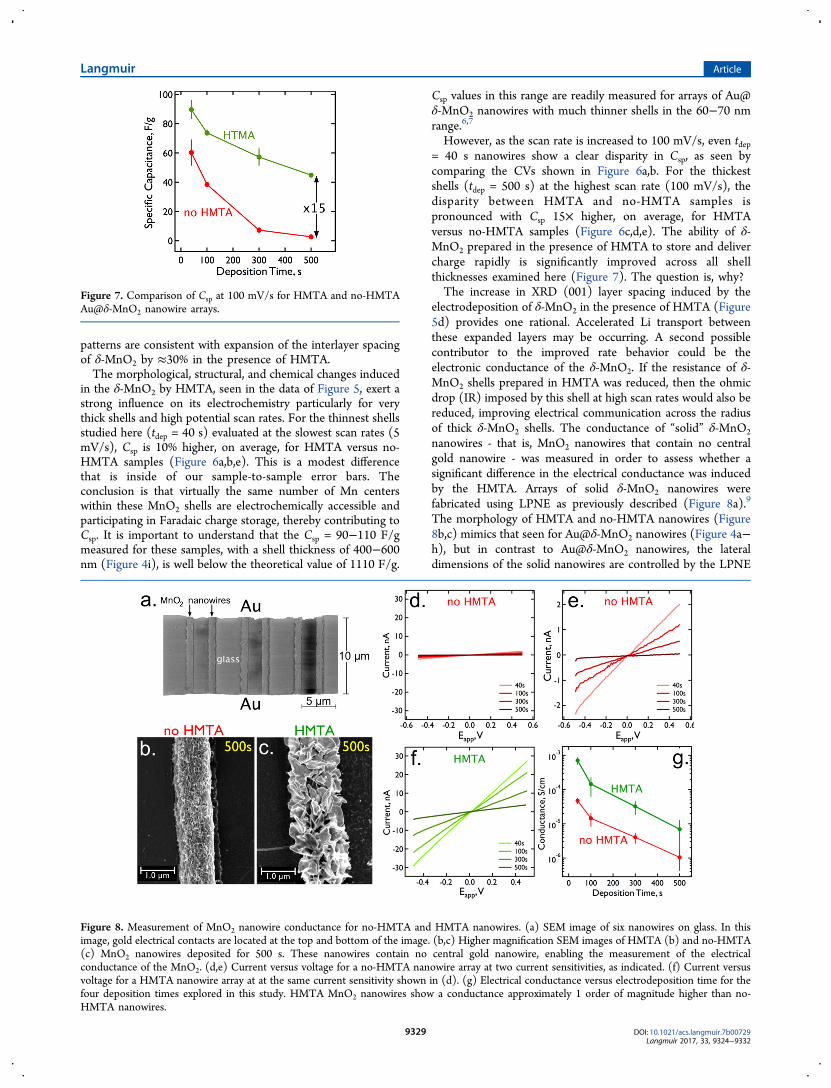
However, as the scan rate is increased to 100 mV/s, even tdep= 40 s nanowires show a clear disparity in Csp, as seen bycomparing the CVs shown in Figure 6a,b. For the thickestshells (tdep = 500 s) at the highest scan rate (100 mV/s), thedisparity between HMTA and no-HMTA samples ispronounced with Csp 15× higher, on average, for HMTAversus no-HMTA samples (Figure 6c,d,e). The ability of δ-MnO2 prepared in the presence of HMTA to store and delivercharge rapidly is significantly improved across all shellthicknesses examined here (Figure 7). The question is, why?The increase in XRD (001) layer spacing induced by the
electrodeposition of δ-MnO2 in the presence of HMTA (Figure5d) provides one rational. Accelerated Li transport betweenthese expanded layers may be occurring. A second possiblecontributor to the improved rate behavior could be theelectronic conductance of the δ-MnO2. If the resistance of δ-MnO2 shells prepared in HMTA was reduced, then the ohmicdrop (IR) imposed by this shell at high scan rates would also bereduced, improving electrical communication across the radiusof thick δ-MnO2 shells. The conductance of “solid” δ-MnO2
nanowires - that is, MnO2 nanowires that contain no centralgold nanowire - was measured in order to assess whether asignificant difference in the electrical conductance was inducedby the HMTA. Arrays of solid δ-MnO2 nanowires werefabricated using LPNE as previously described (Figure 8a).9
The morphology of HMTA and no-HMTA nanowires (Figure8b,c) mimics that seen for Au@δ-MnO2 nanowires (Figure 4a−h), but in contrast to Au@δ-MnO2 nanowires, the lateraldimensions of the solid nanowires are controlled by the LPNE
Figure 7. Comparison of Csp at 100 mV/s for HMTA and no-HMTAAu@δ-MnO2 nanowire arrays.
Figure 8. Measurement of MnO2 nanowire conductance for no-HMTA and HMTA nanowires. (a) SEM image of six nanowires on glass. In thisimage, gold electrical contacts are located at the top and bottom of the image. (b,c) Higher magnification SEM images of HMTA (b) and no-HMTA(c) MnO2 nanowires deposited for 500 s. These nanowires contain no central gold nanowire, enabling the measurement of the electricalconductance of the MnO2. (d,e) Current versus voltage for a no-HMTA nanowire array at two current sensitivities, as indicated. (f) Current versusvoltage for a HMTA nanowire array at at the same current sensitivity shown in (d). (g) Electrical conductance versus electrodeposition time for thefour deposition times explored in this study. HMTA MnO2 nanowires show a conductance approximately 1 order of magnitude higher than no-HMTA nanowires.
Langmuir Article
DOI: 10.1021/acs.langmuir.7b00729Langmuir 2017, 33, 9324−9332
9329
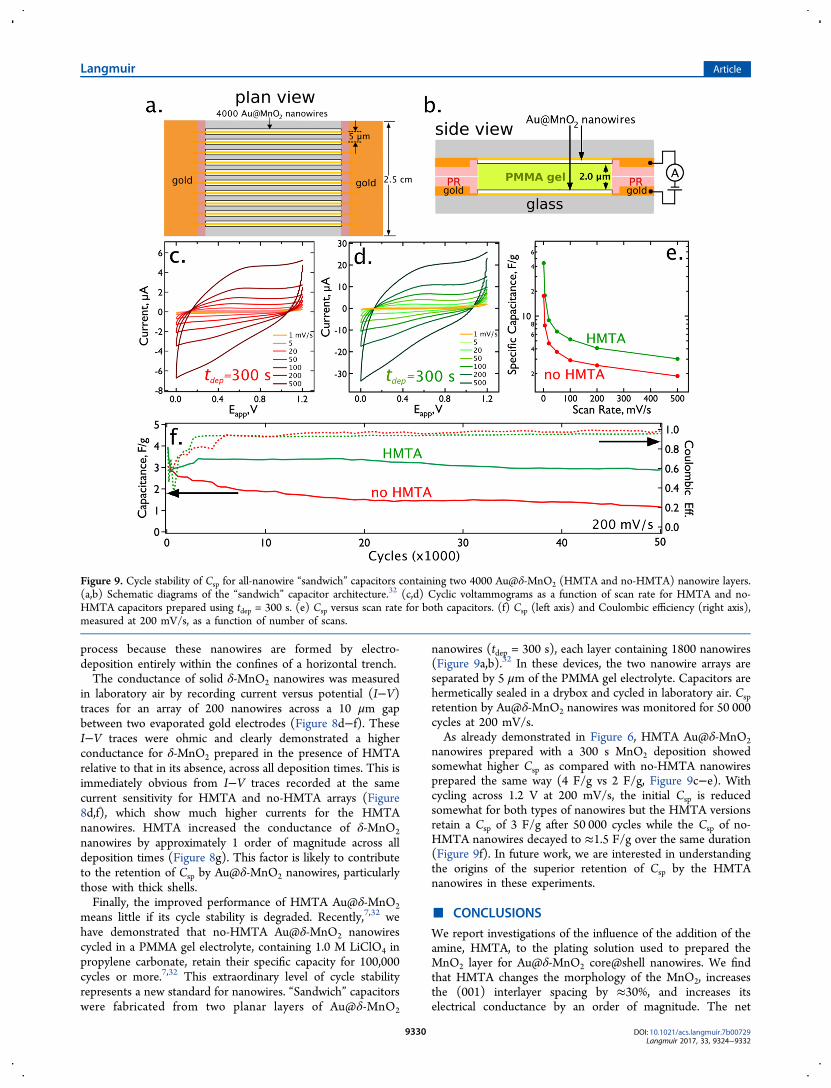
process because these nanowires are formed by electro-deposition entirely within the confines of a horizontal trench.The conductance of solid δ-MnO2 nanowires was measured
in laboratory air by recording current versus potential (I−V)traces for an array of 200 nanowires across a 10 μm gapbetween two evaporated gold electrodes (Figure 8d−f). TheseI−V traces were ohmic and clearly demonstrated a higherconductance for δ-MnO2 prepared in the presence of HMTArelative to that in its absence, across all deposition times. This isimmediately obvious from I−V traces recorded at the samecurrent sensitivity for HMTA and no-HMTA arrays (Figure8d,f), which show much higher currents for the HMTAnanowires. HMTA increased the conductance of δ-MnO2nanowires by approximately 1 order of magnitude across alldeposition times (Figure 8g). This factor is likely to contributeto the retention of Csp by Au@δ-MnO2 nanowires, particularlythose with thick shells.Finally, the improved performance of HMTA Au@δ-MnO2
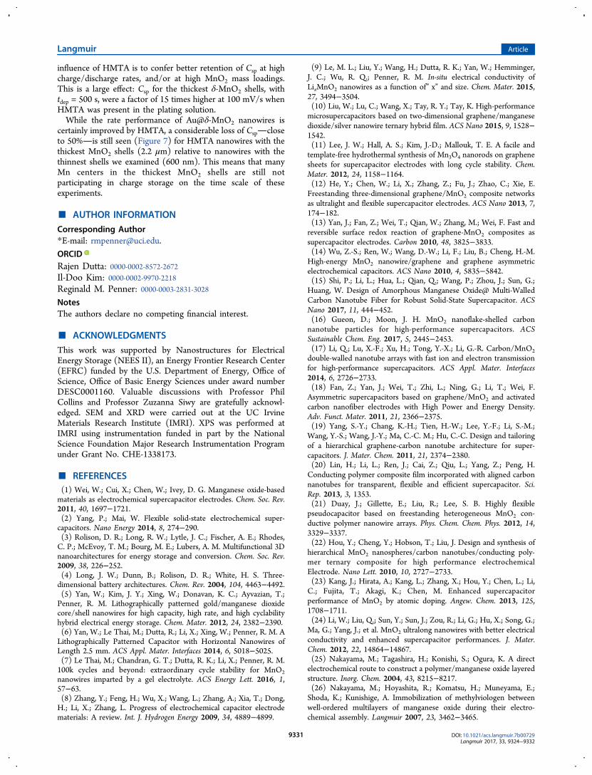
means little if its cycle stability is degraded. Recently,7,32 wehave demonstrated that no-HMTA Au@δ-MnO2 nanowirescycled in a PMMA gel electrolyte, containing 1.0 M LiClO4 inpropylene carbonate, retain their specific capacity for 100,000cycles or more.7,32 This extraordinary level of cycle stabilityrepresents a new standard for nanowires. “Sandwich” capacitorswere fabricated from two planar layers of Au@δ-MnO2
nanowires (tdep = 300 s), each layer containing 1800 nanowires(Figure 9a,b).32 In these devices, the two nanowire arrays areseparated by 5 μm of the PMMA gel electrolyte. Capacitors arehermetically sealed in a drybox and cycled in laboratory air. Cspretention by Au@δ-MnO2 nanowires was monitored for 50 000cycles at 200 mV/s.As already demonstrated in Figure 6, HMTA Au@δ-MnO2
nanowires prepared with a 300 s MnO2 deposition showedsomewhat higher Csp as compared with no-HMTA nanowiresprepared the same way (4 F/g vs 2 F/g, Figure 9c−e). Withcycling across 1.2 V at 200 mV/s, the initial Csp is reducedsomewhat for both types of nanowires but the HMTA versionsretain a Csp of 3 F/g after 50 000 cycles while the Csp of no-HMTA nanowires decayed to ≈1.5 F/g over the same duration(Figure 9f). In future work, we are interested in understandingthe origins of the superior retention of Csp by the HMTAnanowires in these experiments.
■ CONCLUSIONSWe report investigations of the influence of the addition of theamine, HMTA, to the plating solution used to prepared theMnO2 layer for Au@δ-MnO2 core@shell nanowires. We findthat HMTA changes the morphology of the MnO2, increasesthe (001) interlayer spacing by ≈30%, and increases itselectrical conductance by an order of magnitude. The net
Figure 9. Cycle stability of Csp for all-nanowire “sandwich” capacitors containing two 4000 Au@δ-MnO2 (HMTA and no-HMTA) nanowire layers.(a,b) Schematic diagrams of the “sandwich” capacitor architecture.32 (c,d) Cyclic voltammograms as a function of scan rate for HMTA and no-HMTA capacitors prepared using tdep = 300 s. (e) Csp versus scan rate for both capacitors. (f) Csp (left axis) and Coulombic efficiency (right axis),measured at 200 mV/s, as a function of number of scans.
Langmuir Article
DOI: 10.1021/acs.langmuir.7b00729Langmuir 2017, 33, 9324−9332
9330
influence of HMTA is to confer better retention of Csp at highcharge/discharge rates, and/or at high MnO2 mass loadings.This is a large effect: Csp for the thickest δ-MnO2 shells, withtdep = 500 s, were a factor of 15 times higher at 100 mV/s whenHMTA was present in the plating solution.While the rate performance of Au@δ-MnO2 nanowires is
certainly improved by HMTA, a considerable loss of Cspcloseto 50%is still seen (Figure 7) for HMTA nanowires with thethickest MnO2 shells (2.2 μm) relative to nanowires with thethinnest shells we examined (600 nm). This means that manyMn centers in the thickest MnO2 shells are still notparticipating in charge storage on the time scale of theseexperiments.
■ AUTHOR INFORMATION
Corresponding Author*E-mail: [email protected].
ORCIDRajen Dutta: 0000-0002-8572-2672Il-Doo Kim: 0000-0002-9970-2218Reginald M. Penner: 0000-0003-2831-3028NotesThe authors declare no competing financial interest.
■ ACKNOWLEDGMENTS
This work was supported by Nanostructures for ElectricalEnergy Storage (NEES II), an Energy Frontier Research Center(EFRC) funded by the U.S. Department of Energy, Office ofScience, Office of Basic Energy Sciences under award numberDESC0001160. Valuable discussions with Professor PhilCollins and Professor Zuzanna Siwy are gratefully acknowl-edged. SEM and XRD were carried out at the UC IrvineMaterials Research Institute (IMRI). XPS was performed atIMRI using instrumentation funded in part by the NationalScience Foundation Major Research Instrumentation Programunder Grant No. CHE-1338173.
■ REFERENCES(1) Wei, W.; Cui, X.; Chen, W.; Ivey, D. G. Manganese oxide-basedmaterials as electrochemical supercapacitor electrodes. Chem. Soc. Rev.2011, 40, 1697−1721.(2) Yang, P.; Mai, W. Flexible solid-state electrochemical super-capacitors. Nano Energy 2014, 8, 274−290.(3) Rolison, D. R.; Long, R. W.; Lytle, J. C.; Fischer, A. E.; Rhodes,C. P.; McEvoy, T. M.; Bourg, M. E.; Lubers, A. M. Multifunctional 3Dnanoarchitectures for energy storage and conversion. Chem. Soc. Rev.2009, 38, 226−252.(4) Long, J. W.; Dunn, B.; Rolison, D. R.; White, H. S. Three-dimensional battery architectures. Chem. Rev. 2004, 104, 4463−4492.(5) Yan, W.; Kim, J. Y.; Xing, W.; Donavan, K. C.; Ayvazian, T.;Penner, R. M. Lithographically patterned gold/manganese dioxidecore/shell nanowires for high capacity, high rate, and high cyclabilityhybrid electrical energy storage. Chem. Mater. 2012, 24, 2382−2390.(6) Yan, W.; Le Thai, M.; Dutta, R.; Li, X.; Xing, W.; Penner, R. M. ALithographically Patterned Capacitor with Horizontal Nanowires ofLength 2.5 mm. ACS Appl. Mater. Interfaces 2014, 6, 5018−5025.(7) Le Thai, M.; Chandran, G. T.; Dutta, R. K.; Li, X.; Penner, R. M.100k cycles and beyond: extraordinary cycle stability for MnO2nanowires imparted by a gel electrolyte. ACS Energy Lett. 2016, 1,57−63.(8) Zhang, Y.; Feng, H.; Wu, X.; Wang, L.; Zhang, A.; Xia, T.; Dong,H.; Li, X.; Zhang, L. Progress of electrochemical capacitor electrodematerials: A review. Int. J. Hydrogen Energy 2009, 34, 4889−4899.
(9) Le, M. L.; Liu, Y.; Wang, H.; Dutta, R. K.; Yan, W.; Hemminger,J. C.; Wu, R. Q.; Penner, R. M. In-situ electrical conductivity ofLixMnO2 nanowires as a function of” x” and size. Chem. Mater. 2015,27, 3494−3504.(10) Liu, W.; Lu, C.; Wang, X.; Tay, R. Y.; Tay, K. High-performancemicrosupercapacitors based on two-dimensional graphene/manganesedioxide/silver nanowire ternary hybrid film. ACS Nano 2015, 9, 1528−1542.(11) Lee, J. W.; Hall, A. S.; Kim, J.-D.; Mallouk, T. E. A facile andtemplate-free hydrothermal synthesis of Mn3O4 nanorods on graphenesheets for supercapacitor electrodes with long cycle stability. Chem.Mater. 2012, 24, 1158−1164.(12) He, Y.; Chen, W.; Li, X.; Zhang, Z.; Fu, J.; Zhao, C.; Xie, E.Freestanding three-dimensional graphene/MnO2 composite networksas ultralight and flexible supercapacitor electrodes. ACS Nano 2013, 7,174−182.(13) Yan, J.; Fan, Z.; Wei, T.; Qian, W.; Zhang, M.; Wei, F. Fast andreversible surface redox reaction of graphene-MnO2 composites assupercapacitor electrodes. Carbon 2010, 48, 3825−3833.(14) Wu, Z.-S.; Ren, W.; Wang, D.-W.; Li, F.; Liu, B.; Cheng, H.-M.High-energy MnO2 nanowire/graphene and graphene asymmetricelectrochemical capacitors. ACS Nano 2010, 4, 5835−5842.(15) Shi, P.; Li, L.; Hua, L.; Qian, Q.; Wang, P.; Zhou, J.; Sun, G.;Huang, W. Design of Amorphous Manganese Oxide@ Multi-WalledCarbon Nanotube Fiber for Robust Solid-State Supercapacitor. ACSNano 2017, 11, 444−452.(16) Gueon, D.; Moon, J. H. MnO2 nanoflake-shelled carbonnanotube particles for high-performance supercapacitors. ACSSustainable Chem. Eng. 2017, 5, 2445−2453.(17) Li, Q.; Lu, X.-F.; Xu, H.; Tong, Y.-X.; Li, G.-R. Carbon/MnO2
double-walled nanotube arrays with fast ion and electron transmissionfor high-performance supercapacitors. ACS Appl. Mater. Interfaces2014, 6, 2726−2733.(18) Fan, Z.; Yan, J.; Wei, T.; Zhi, L.; Ning, G.; Li, T.; Wei, F.Asymmetric supercapacitors based on graphene/MnO2 and activatedcarbon nanofiber electrodes with High Power and Energy Density.Adv. Funct. Mater. 2011, 21, 2366−2375.(19) Yang, S.-Y.; Chang, K.-H.; Tien, H.-W.; Lee, Y.-F.; Li, S.-M.;Wang, Y.-S.; Wang, J.-Y.; Ma, C.-C. M.; Hu, C.-C. Design and tailoringof a hierarchical graphene-carbon nanotube architecture for super-capacitors. J. Mater. Chem. 2011, 21, 2374−2380.(20) Lin, H.; Li, L.; Ren, J.; Cai, Z.; Qiu, L.; Yang, Z.; Peng, H.Conducting polymer composite film incorporated with aligned carbonnanotubes for transparent, flexible and efficient supercapacitor. Sci.Rep. 2013, 3, 1353.(21) Duay, J.; Gillette, E.; Liu, R.; Lee, S. B. Highly flexiblepseudocapacitor based on freestanding heterogeneous MnO2 con-ductive polymer nanowire arrays. Phys. Chem. Chem. Phys. 2012, 14,3329−3337.(22) Hou, Y.; Cheng, Y.; Hobson, T.; Liu, J. Design and synthesis ofhierarchical MnO2 nanospheres/carbon nanotubes/conducting poly-mer ternary composite for high performance electrochemicalElectrode. Nano Lett. 2010, 10, 2727−2733.(23) Kang, J.; Hirata, A.; Kang, L.; Zhang, X.; Hou, Y.; Chen, L.; Li,C.; Fujita, T.; Akagi, K.; Chen, M. Enhanced supercapacitorperformance of MnO2 by atomic doping. Angew. Chem. 2013, 125,1708−1711.(24) Li, W.; Liu, Q.; Sun, Y.; Sun, J.; Zou, R.; Li, G.; Hu, X.; Song, G.;Ma, G.; Yang, J.; et al. MnO2 ultralong nanowires with better electricalconductivity and enhanced supercapacitor performances. J. Mater.Chem. 2012, 22, 14864−14867.(25) Nakayama, M.; Tagashira, H.; Konishi, S.; Ogura, K. A directelectrochemical route to construct a polymer/manganese oxide layeredstructure. Inorg. Chem. 2004, 43, 8215−8217.(26) Nakayama, M.; Hoyashita, R.; Komatsu, H.; Muneyama, E.;Shoda, K.; Kunishige, A. Immobilization of methylviologen betweenwell-ordered multilayers of manganese oxide during their electro-chemical assembly. Langmuir 2007, 23, 3462−3465.
Langmuir Article
DOI: 10.1021/acs.langmuir.7b00729Langmuir 2017, 33, 9324−9332
9331
(27) Nakayama, M.; Shamoto, M.; Kamimura, A. Surfactant-inducedelectrodeposition of layered manganese oxide with large interlayerspace for catalytic oxidation of phenol. Chem. Mater. 2010, 22, 5887−5894.(28) Nakayama, M.; Fujii, Y.; Fujimoto, K.; Yoshimoto, M.; Kaide,A.; Saeki, T.; Asada, H. Electrochemical synthesis of a nanohybrid filmconsisting of stacked graphene sheets and manganese oxide as oxygenevolution reaction catalyst. RSC Adv. 2016, 6, 23377−23382.(29) Xiang, C.; Yang, Y.; Penner, R. M. Cheating the DiffractionLimit: Electrodeposited Nanowires Patterned by Photolithography.Chem. Commun. 2009, 859−873.(30) Xiang, C.; Kung, S.-C.; Taggart, D. K.; Yang, F.; Thompson, M.A.; Guell, A. G.; Yang, Y.; Penner, R. M. Lithographically patternednanowire electrodeposition: a method for patterning electricallycontinuous metal nanowires on dielectrics. ACS Nano 2008, 2,1939−1949.(31) Menke, E. J.; Thompson, M. A.; Xiang, C.; Yang, L. C.; Penner,R. M. Lithographically patterned nanowire electrodeposition. Nat.Mater. 2006, 5, 914−919.(32) Le Thai, M.; Qiao, S.; Dutta, R. K.; Jha, G.; Ogata, A.;Chandran, G. T.; Penner, R. M. Collateral advantages of a gelelectrolyte for MnO2 nanowire capacitors: higher voltage; reducedvolume. ACS Energy Lett. 2017, 1162−1169.(33) Cooney, A. P.; Crampton, M. R.; Golding, P. The acid−basebehaviour of hexamine and its N-acetyl derivatives. J. Chem. Soc., PerkinTrans. 2 1986, 835−839.(34) Dowding, J. M.; Das, S.; Kumar, A.; Dosani, T.; McCormack, R.;Gupta, A.; Sayle, T. X.; Sayle, D. C.; von Kalm, L.; Seal, S.; et al.Cellular interaction and toxicity depend on physicochemical propertiesand surface modification of redox-active nanomaterials. ACS Nano2013, 7, 4855−4868.(35) Dementjev, A.; De Graaf, A.; Van de Sanden, M.; Maslakov, K.;Naumkin, A.; Serov, A. X-ray photoelectron spectroscopy referencedata for identification of the C 3 N 4 phase in carbon-nitrogen films.Diamond Relat. Mater. 2000, 9, 1904−1907.(36) Mu, B.; Zhang, W.; Shao, S.; Wang, A. Glycol assisted synthesisof graphene−MnO2−polyaniline ternary composites for high perform-ance supercapacitor electrodes. Phys. Chem. Chem. Phys. 2014, 16,7872−7880.
Langmuir Article
DOI: 10.1021/acs.langmuir.7b00729Langmuir 2017, 33, 9324−9332
9332