Embed Size (px)
Citation preview
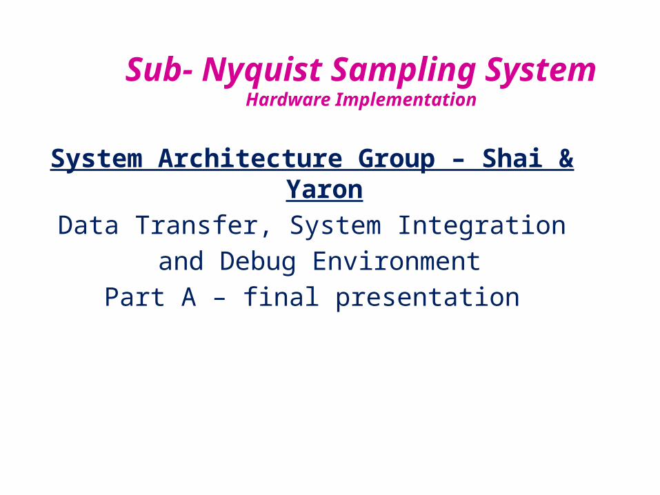
Sub- Nyquist Sampling SystemHardware Implementation
System Architecture Group – Shai & YaronData Transfer, System Integration
and Debug EnvironmentPart A – final presentation
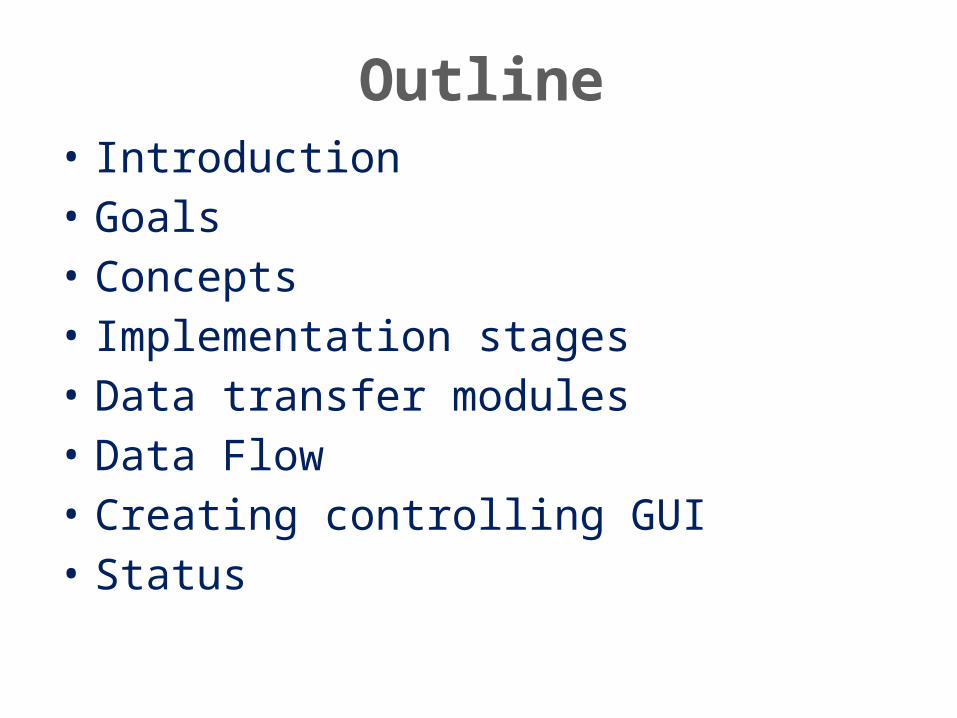
Outline• Introduction• Goals• Concepts• Implementation stages• Data transfer modules• Data Flow• Creating controlling GUI• Status
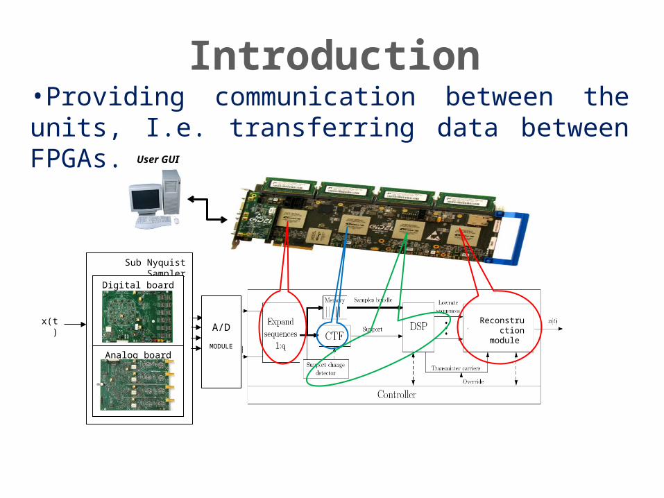
Sub Nyquist Sampler
Digital board
Analog board
x(t)A/D
MODULE
User GUI
Reconstruction module
•Providing communication between the units, I.e. transferring data between FPGAs.
Introduction
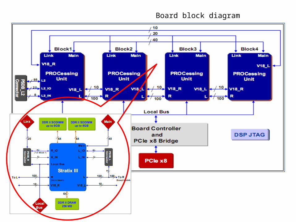
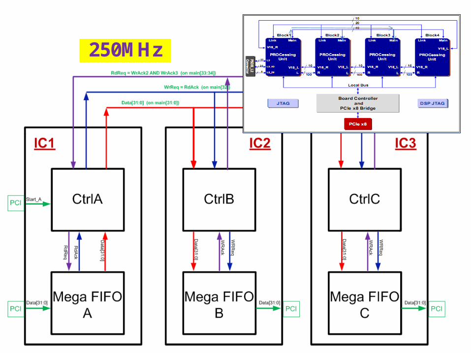
Board block diagram
• Expander, CTF and DSP must communicate using the board resources.
• The communication must be efficient and reliable.• The system must have a debug environment for the
whole units together and separately.• The debug environment must be easy to use and
requires a GUI
Goals
• Sub-Nyquist sampling system architecture assembles 3 FPGAs to one electrical circuit composed from few different logical units.
• Each FPGA contain 1, or more, of these logical units.• Since each unit needs to communicate with the other
units, there is a need to implement special units for communicating between FGPAs.
• Large amount of data needs to be transferred between FPGAs using very limited resources.
Concepts
• The whole communication between the FPGAs and the PCI should work flawless, and so, requires a debug environment for the system, in addition to a debug environment for each FPGA by itself.
Concepts
• Learning the ProcStar board and Its abilities:transferring data between FPGAs using Quartos FIFOs and the board’s BUSes.
Implementation Stages
250MHz
• Learning the ProcStar board and Its abilities:transferring data between FPGAs using Quartos FIFOsand the board’s BUSes.
• Transferring DATA between FPGAs on board, using Registers and Mega-FIFOs: DATA transferred through Internal FIFO with different Clock Frequencies on input and output ports.doing so, we learnt to transfer large amount of data (more than 200 bits) over the Main BUS (40 bits only).
Implementation Stages
• Building Debug Environment for communication between FPGAs, using a Black Box approach inside FPGA, instead of real Hardware.
Implementation Stages
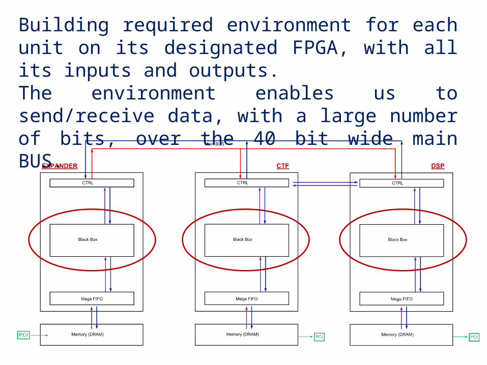
Building required environment for each unit on its designated FPGA, with all its inputs and outputs.The environment enables us to send/receive data, with a large number of bits, over the 40 bit wide main BUS.
• Building Debug Environment for communication between FPGAs, using a Black Box approach inside FPGA, instead of real Hardware.
• Debug the environment with a temporary GUI.
Implementation Stages
• Building Debug Environment for communication between FPGAs, using a Black Box approach inside FPGA, instead of real Hardware.
• Debug the environment with a temporary GUI.• In the process of implementing the required Debug
Environment there was a need to implement our own transition devices, due to non-standard requirements of the logical units.
Implementation Stages
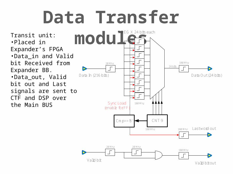
Data Transfer modulesTransit unit:•Placed in Expander’s FPGA•Data_in and Valid bit Received from Expander BB.•Data_out, Valid bit out and Last signals are sent to CTF and DSP over the Main BUS
CNT 9Cmp==’8'
Data In (216 bits)
9 REG X 24 bits each
Valid bit
Data Out (24 bits)
Last word out
Valid bit out
Sync Load(enable for FF)
24 bits
24 bits
180 Mhz
180 Mhz
20 Mhz
20 Mhz 20 Mhz180 Mhz
180 Mhz180 Mhz
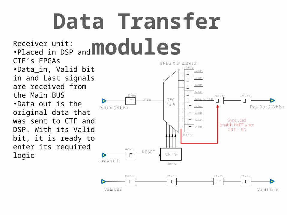
Data Transfer modulesReceiver unit:•Placed in DSP and CTF’s FPGAs•Data_in, Valid bit in and Last signals are received from the Main BUS•Data out is the original data that was sent to CTF and DSP. With its Valid bit, it is ready to enter its required logic
CNT 9
Data In (24 bits)
9 REG X 24 bits each
Valid bit in
Data Out (216 bits)
Last word in
Valid bit out
24 bits
20 Mhz180 Mhz
180 Mhz
180 Mhz
RESET
24 bits
180 Mhz
180 Mhz
24 bits
24 bits
24 bits
24 bits
24 bits
24 bits
24 bits
24 bits
24 bits
216 bits
Sync Load(enable for FF when
CNT = ‘0’)
180 Mhz
DEC1à 9
20 Mhz 20 Mhz 20 Mhz
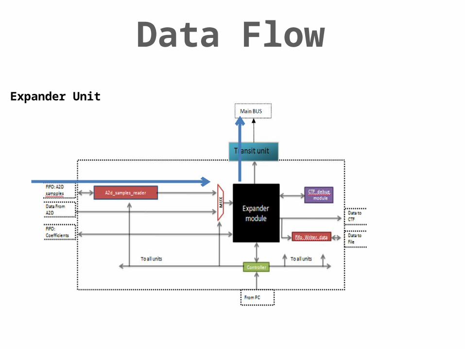
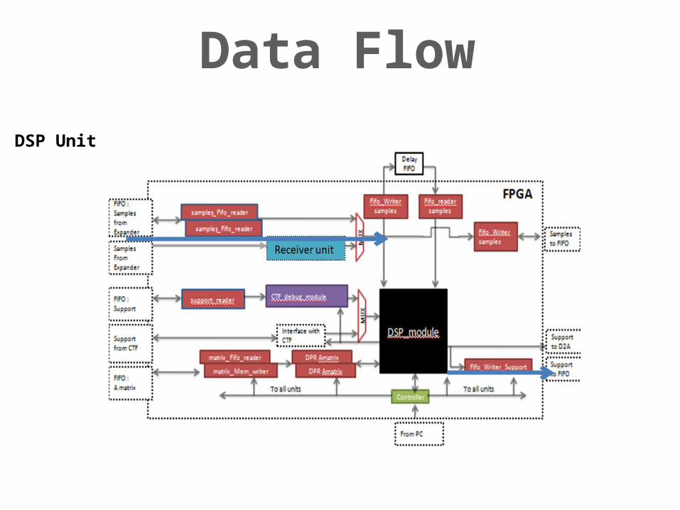
Data Flow
Expander Unit
Data Flow
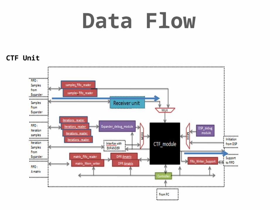
CTF Unit
Data Flow
DSP Unit
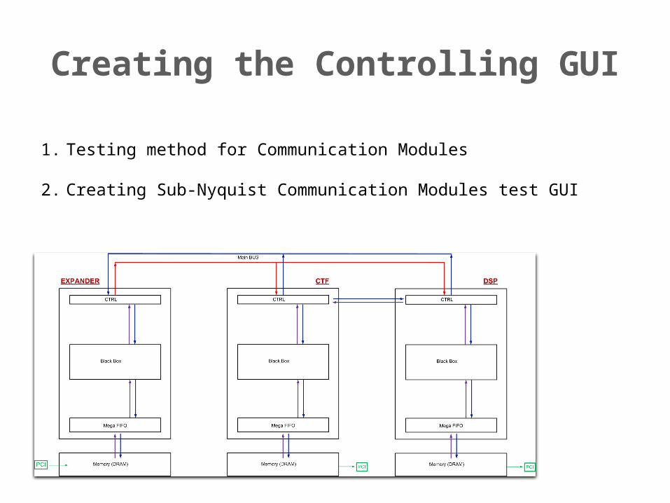
Creating the Controlling GUI
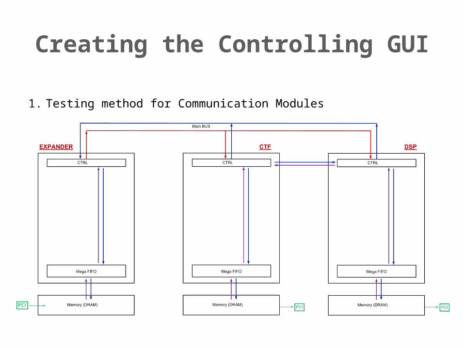
Creating the Controlling GUI
1. Testing method for Communication Modules
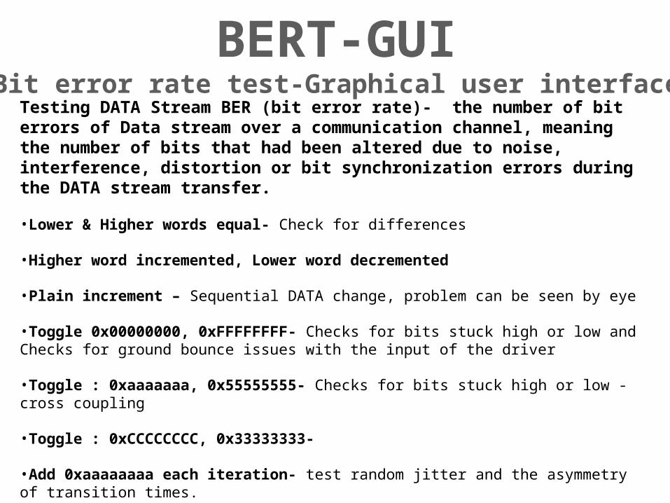
BERT-GUIBit error rate test-Graphical user interface
Testing DATA Stream BER (bit error rate)- the number of bit errors of Data stream over a communication channel, meaning the number of bits that had been altered due to noise, interference, distortion or bit synchronization errors during the DATA stream transfer.
•Lower & Higher words equal- Check for differences
•Higher word incremented, Lower word decremented
•Plain increment – Sequential DATA change, problem can be seen by eye
•Toggle 0x00000000, 0xFFFFFFFF- Checks for bits stuck high or low and Checks for ground bounce issues with the input of the driver
•Toggle : 0xaaaaaaa, 0x55555555- Checks for bits stuck high or low - cross coupling
•Toggle : 0xCCCCCCCC, 0x33333333-
•Add 0xaaaaaaaa each iteration- test random jitter and the asymmetry of transition times.
•1-HOT- Pattern contains the longest string of consecutive zeros with the lowest ones density
•0-HOT- Pattern contains the longest string of consecutive zeros with the lowest ones density
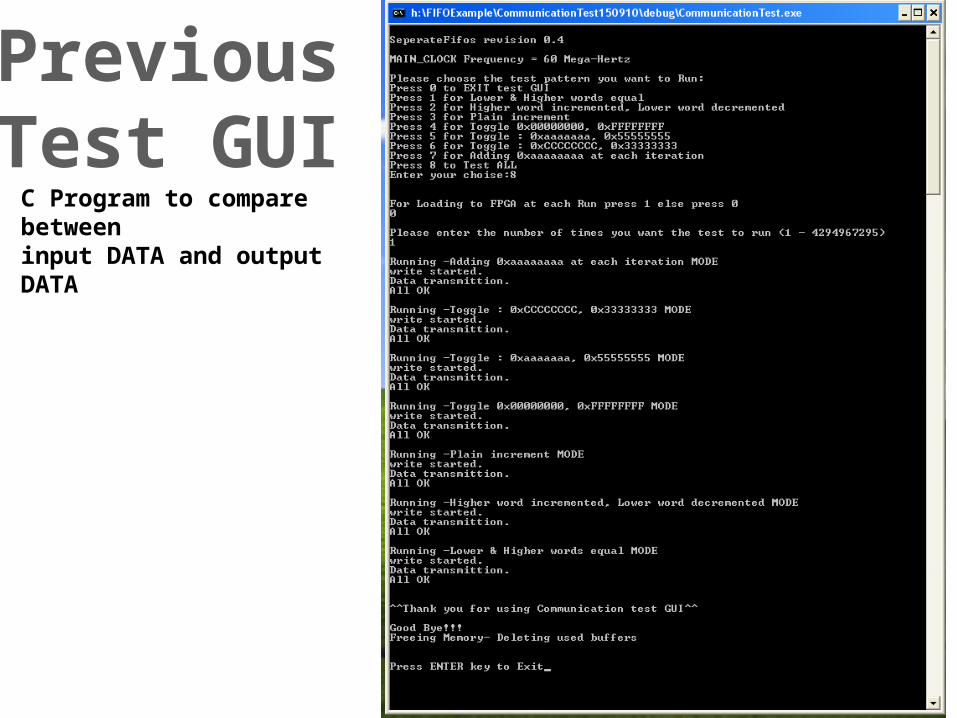
PreviousTest GUI
C Program to compare between input DATA and output DATA
Creating the Controlling GUI
1. Testing method for Communication Modules
2. Creating Sub-Nyquist Communication Modules test GUI
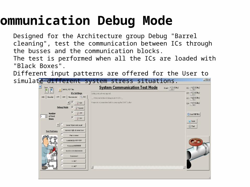
Designed for the Architecture group Debug "Barrel cleaning", test the communication between ICs through the busses and the communication blocks.The test is performed when all the ICs are loaded with "Black Boxes".Different input patterns are offered for the User to simulate different system stress situations.
Communication Debug Mode
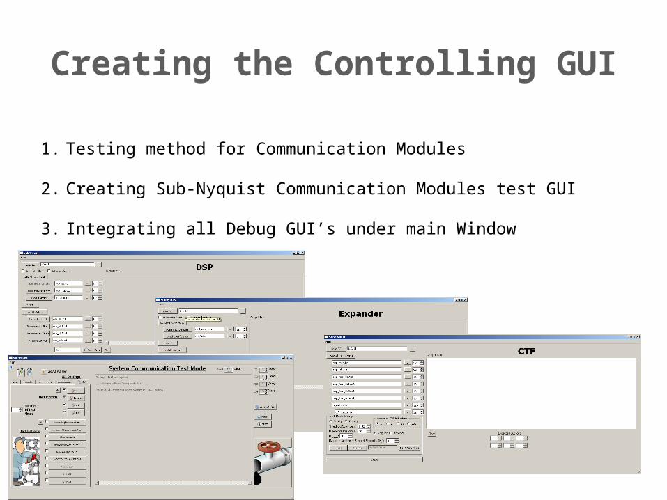
Creating the Controlling GUI
1. Testing method for Communication Modules
2. Creating Sub-Nyquist Communication Modules test GUI
3. Integrating all Debug GUI’s under main Window
Creating the Controlling GUI
1. Testing method for Communication Modules
2. Creating Sub-Nyquist Communication Modules test GUI
3. Integrating all Debug GUI’s under main Window
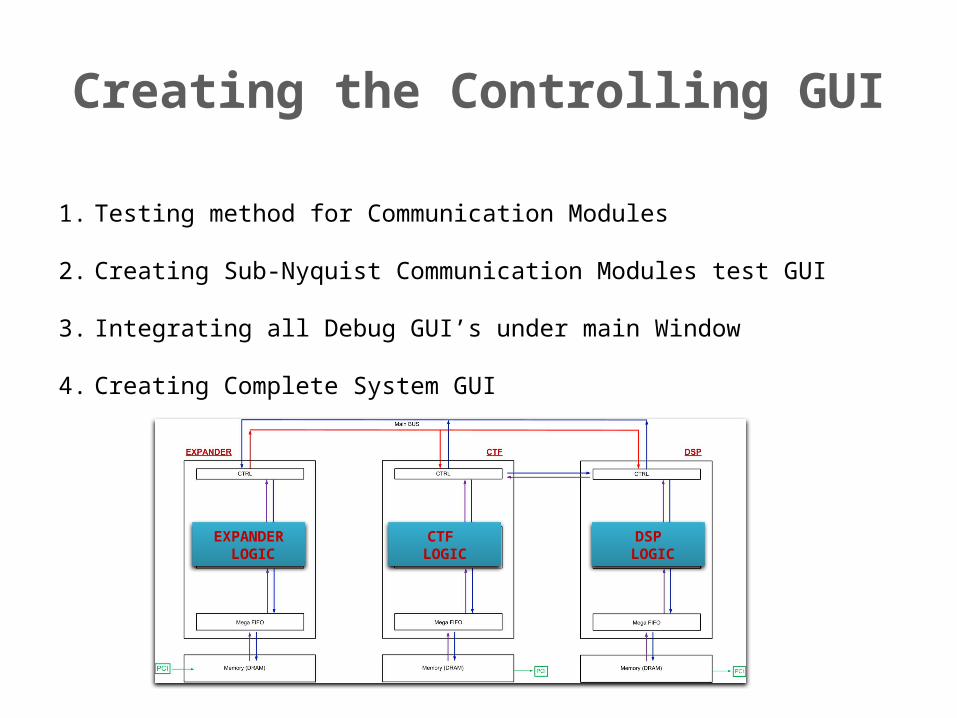
4. Creating Complete System GUI
DSP LOGIC
CTF LOGIC
EXPANDER LOGIC
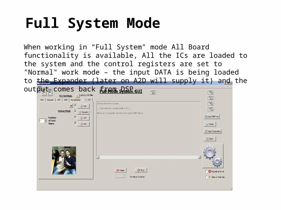
When working in “Full System" mode All Board functionality is available, All the ICs are loaded to the system and the control registers are set to "Normal" work mode – the input DATA is being loaded to the Expander (later on A2D will supply it) and the output comes back from DSP.
Full System Mode
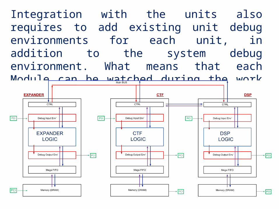
Integration with the units also requires to add existing unit debug environments for each unit, in addition to the system debug environment. What means that each Module can be watched during the work of the complete system
Creating the Controlling GUI
1. Testing method for Communication Modules
2. Creating Sub-Nyquist Communication Modules test GUI
3. Integrating all Debug GUI’s under main Window
4. Creating Complete System GUI
5. Future aspirations
5.1 Fixing Mega-FIFO error5.2 Adding missing Modules to the GUI5.3 Correct separate Modules Debug GUI’s5.4 Adding functionality to the – “Entire System” GUI5.5 Debugging the Entire System (all Modules loaded) using the GUI
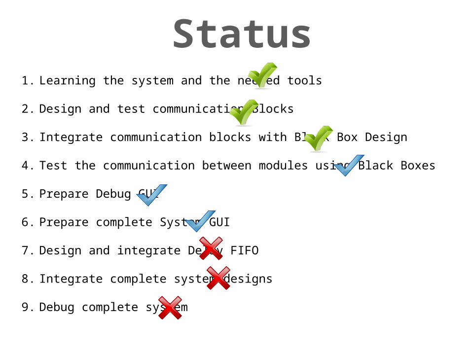
Status1. Learning the system and the needed tools
2. Design and test communication Blocks
3. Integrate communication blocks with Black Box Design
4. Test the communication between modules using Black Boxes
5. Prepare Debug GUI
6. Prepare complete System GUI
7. Design and integrate Delay FIFO
8. Integrate complete system designs
9. Debug complete system
Questions?