Embed Size (px)
Citation preview

SU-8 and PDMS Based Hybrid Fabrication Technology for
Combination of Permanently Bonded Flexible and Rigid Features
on a Single Device
Jasbir N. Patel1, Bonnie L. Gray
1, Bozena Kaminska
1, Nien-Chen Wu
2 and Byron D. Gates
2
1 School of Engineering Science, Simon Fraser University, Burnaby, BC, V5A 1S6 Canada.
2 Department of Chemistry, Simon Fraser University, Burnaby, BC, V5A 1S6 Canada.
Abstract
In this article, a novel hybrid fabrication technology is presented that uses both a flexible
polymer (polydimethylsiloxane - PDMS) and a rigid polymer (SU-8). A covalent bond between
the flexible and rigid polymer layers is achieved using an oxygen plasma treatment during a
layer-by-layer direct spin-on process. Precise alignment of the features in each layer and a
highly repeatable method are achieved by this new process.
As a proof-of-concept, we successfully fabricated PDMS-based flexible microfluidic
devices with SU-8-based rigid world-to-chip/chip-to-world interconnects. The bond strength
between the PDMS and SU-8 layers is measured by three methods: 1) Instron®
microtester to
pull apart the layers; 2) voice coil actuator to test the bond between interconnects and the
substrate; and 3) microfluidic pressurization test to evaluate the bond strength along the channels.
The bond strength between the flexible PDMS layer and the rigid SU-8 features is very strong;
the bond between these two polymers does not fail during these evaluations although the
integrity of the PDMS layer itself fails during the microtester evaluation. Additionally, the layer-
by-layer direct-spin on process resulted in a repeatable process and precise alignment of the
features in each layer, which are necessary in order to achieve consistent performance from the
fabricated devices.
The rigid SU-8 interconnects fabricated onto a flexible PDMS device serve as a world-to-
chip/chip-to-world interconnects for the direct connection with Tygon® tubing. Three different
designs of hybrid (PDMS and SU-8 based) microfluidic devices are designed, fabricated and
tested. Each variation differed in the microchannel design in order to demonstrate the versatility
of the process to make devices on multiple scales and patterns. These hybrid microfluidic
devices are capable of functioning without leakage up to pressures of 85.85 ±3.56 kPa. Although
microfluidic channels with interconnects are shown as a proof-of-concept, the fabrication
process demonstrated herein could be utilized to develop a number of more sophisticated
microfluidic and biomedical devices.
Final version published as:"SU-8 and PDMS-based Hybrid Fabrication Technology for Combination of Permanently Bonded Flexible and Rigid Features on a Single Device," Patel, J.N.; Gray, B.L.; Kaminska, B.; Wu, N.-C.; Gates, B.D., J. Micromech. Microeng. 2013, 23, 065029. DOI: 10.1088/0960-1317/23/6/065029.

1 Introduction & background
SU-8 and PDMS have been widely used for many years as the polymers of choice in the
fabrication of a number of different polymer-based microfabrication processes. Initially, PDMS
and SU-8 were mainly used to fabricate devices with microfluidic or biomedical applications [1-
3] and SU-8 was additionally used to make molds for PDMS based flexible devices [1-3]. SU-8
has also been used in the fabrication of active devices, such as gears, and actuators [4]. PDMS is
a desirable material in the fabrication of microfluidics because of its proven bio-compatibility [5],
over-all flexibility and relatively low materials cost.
Generally, PDMS is used for fabricating flexible devices and SU-8 is used for fabricating
rigid and strong micro-structures. Until now, systems that include a combination of rigid and
flexible polymers have been realized using PDMS and other rigid substrate materials, such as
glass, PMMA and silicon [6-8]. In such micro-systems, the PDMS based flexible features and
the other rigid features were fabricated separately and combined in the end by surface treatment
of the PDMS followed by bonding at the interface of these dissimilar materials. Besides, rigid
layers are generally used as a base substrate upon which the devices are built, and primarily used
for metal connections or structural rigidity. Hence, the over-all flexibility of the completed
device is lost in such cases. Additionally, the existing approaches have limitations in the
precision in the alignment of bonded features.
In many cases, it is desirable to fabricate rigid structures directly on flexible devices
without sacrificing over-all flexibility of the resulting device. An example of a potential
application of these hybrid structures are rigid microfluidic interconnects integrated directly onto
a flexible microfluidic chip. These rigid interconnects can be used for chip-to-chip and/or chip-
to-world/world-to-chip interconnects. It has been shown that combinations of rigid and flexible
materials usually result in the most robust interconnects [9].
Previously, microfluidic chips with interconnect structures were fabricated either using a
flexible polymer material (e.g., PDMS) or rigid polymer materials (e.g., SU-8) [9]. However, in
these previous designs, the connections between the device and the “world” were fabricated
using the same material as the microfluidic chips (i.e. SU-8 interconnects onto the SU-8
microfluidic chips, and PDMS interconnects onto the PDMS microfluidic chips). SU-8 based
microfluidic chips with SU-8 interconnects worked well for chip-to-chip and/or world-to-
chip/chip-to-world connections. However, the PDMS interconnects based chips were difficult to
align and connect together because of the inherent characteristics of the PDMS, such as stiction
between surfaces and structural deformation.
Building rigid interconnects on a flexible device would make these structures more
functional and adaptable to a wide variety of applications. Hence, a fabrication technology that
can incorporate the rigid (e.g., SU-8) interconnect structures directly onto the flexible (e.g.,
PDMS) microfluidic device is required for such devices. Fabrication procedures need to be

developed that can incorporate rigid interconnect structures directly onto the PDMS layer.
Additionally, to the best of our knowledge there is no direct spin-on and self-registration process
demonstrated in the literature for fabricating rigid polymer structures on top of any other flexible
polymer support.
We present here in a fabrication method to fabricate SU-8-based microstructures directly
onto flexible PDMS based devices. This fabrication process features a layer-by-layer direct
spin-on process to prepare an SU-8 layer on top of a PDMS support. Using this new approach,
we are able to align multiple layers of PDMS and/or SU-8 that may be useful in more complex
designs and applications. The proposed fabrication technology also incorporates a strong
adhesion between the PDMS and the SU-8 layers. Using the hybrid fabrication technology, fully
flexible microfluidic devices (PDMS-based) are fabricated with the rigid (SU-8) interconnects
directly patterned onto the fluidic inlet/outlet ports. The devices presented here are merely for a
proof-of-concept, but the capabilities of this technology are not limited to this simple
demonstration. Many more complex biomedical and microfluidic devices could be possible
using the proposed fabrication technology.
2 Fabrication principle and hypothesis
In this section, a detailed explanation is provided to describe the hybrid fabrication
technology to make flexible devices using both the SU-8 and PDMS polymers. First, the hybrid
fabrication principle is explained using the simplified process of the proposed technology. And
finally, different designs of the hybrid microfluidic devices are described based on the
fabrication technology.
2.1 Fabrication principles
In this section, a simplified set of fabrication steps are briefly described for our new
fabrication process. The fabrication process for preparing the SU-8 molds for the patterning of
PDMS microfluidic devices to be used as the patterned base layer of our device (PDMS) are not
described in detail here. These are relatively well known technologies [10]. Details are provided
for the fabrication process to make hybrid microfluidic devices (see Section 2.4). The cured,
patterned PDMS layer served as the base layer for demonstrating our new approach to making
hybrid devices. The exact process parameters for patterning the SU-8 layer(s) were adopted
from previous experiments [11][12], and are not elaborated upon in further detail within this
manuscript. We do, however, explain the important process steps and considerations necessary
to achieve a permanently bonded SU-8 layer onto the PDMS layer by direct spin-on process.
The simplified fabrication process of the proposed hybrid fabrication technology is
shown in Figure 1. In the first step of this fabrication process, the PDMS layer was prepared on
a clean glass substrate using standard soft lithography techniques (Figure 1(a)). This PDMS
layer was exposed to the oxygen (O2) plasma (using an Axic Benchmark 800 Plasma System) to

activate the surfaces of the PDMS (Figure 1(b)). An appropriate formulation of the SU-8 layer
was spun (using Headway Research Inc. spin coater) onto the PDMS layer directly after the
preparation of the activated PDMS surfaces (Figure 1(c)). It is very important to coat the SU-8
layer onto the activated PDMS as soon as possible in order to form the strongest bond between
these two polymer layers (PDMS and SU-8). A detailed explanation for a possible mechanism
behind the strong interactions between the SU-8 and PDMS are discussed in Section 2.2. A
specific formulation of the SU-8 and spin coating parameters were used to achieve the desired
thickness of the SU-8 layer as described in prior literature [11][12]. The SU-8 layer was soft
baked on a hot plate (Torrey Pines Scientific EchoTherm HS40) followed by exposure to UV
light (using Quintel Corporation Q-2001CT) through an appropriate photolithography mask
(Figure 1(d)). The UV exposed SU-8 layer was heated again for the post-exposure bake process
(Figure 1(e)), cooled to room temperature and immersed in an SU-8 developer bath composed of
propylene-glycol-monoether-acetate (PGMEA) (Figure 1(f)). This SU-8 developer dissolved the
uncrosslinked SU-8. Finally, the PDMS layer and the permanently bonded SU-8 structures were
peeled-off from the glass substrate (Figure 1(g)).
The resulting hybrid, free-standing polymer stack contained a PDMS base layer and
patterned SU-8, which was permanently bonded to the PDMS to provide a combination of
Figure 1: The simplified hybrid fabrication process:(a) On a cleaned substrate, pour and cure a mixture of the
Sylgard 184 (PDMS) elastomer and its curing agent; (b) expose the PDMS layer to an O2 plasma to activate the
surface; (c) spin the appropriate SU-8 formulation for the desired thickness of SU-8 and soft-bake this layer with
the parameters defined previously [11];(d) selectively expose the SU-8 layer to a UV source using the desired
mask pattern;(e) heat the SU-8 layer for the post exposure bake;(f) remove the uncrosslinked SU-8 using the SU-
8 developer; and (g) peel-off the hybrid polymer stack from the base substrate.

flexibility and rigidity combination with precise alignment of the features in both layers.
2.2 Hypothesis behind the hybrid fabrication technology
Previously, the SU-8 structures were directly prepared on a PDMS layer to obtain easily
peel-able SU-8 devices [11] or SU-8 based sacrificial layers [12]. These stand-alone SU-8
structures were easily fabricated because the adhesion of the SU-8 layer with the PDMS layer is
inherently poor. Additionally, the SU-8 is a mechanically rigid material whereas the PDMS is a
mechanically flexible material, which helps to detach the fully processed SU-8 layer just by
mechanical bending the PDMS layer [11][12].
We introduce herein a hybrid polymer stack incorporating both the PDMS and SU-8
layers with a strong bond between these two polymer layers. To achieve a strong adhesion
between these two materials, the PDMS surfaces were treated with oxygen plasma before the
SU-8 layer was spun onto the PDMS. In the previous technologies [11][12], the PDMS surface
was not treated by any means before processing the SU-8 layer on the surfaces of the PDMS.
Hence, the additional step of oxygen plasma treatment created a strong bond between the PDMS
and SU-8 layers. All the other SU-8 processing steps, such as the soft bake, the post-exposure
bake, the UV exposure, the solvent development and the hard bake remained identical in both
methodologies.
The cured PDMS contains repeating chains of dimethylsiloxane units (-O-Si(CH3)2-)x.
Exposing these polymer chains to oxygen plasma creates silanol groups (Si-OH) on the PDMS
surfaces [13][14]. It has previously been demonstrated that the epoxy groups of SU-8 can
strongly bond with the (Si-O) groups of silanol on the exterior of plasma treated PDMS surfaces
(or SiO2) [15]. The SU-8 polymer chain can, therefore, strongly bond with the functional groups
generated by the oxygen plasma treatment of the PDMS surfaces.
In order to demonstrate a successful proof-of-concept, we used surface activation
parameters that were optimized in prior experiments [13]. In future, this study could be further
extended to determine the influence of different activation parameters on quality of the hybrid
flexible structures created by processes described herein.
3 Design and fabrication of the hybrid microfluidic devices
After optimizing the SU-8 and PDMS based technology, we designed and made a proof-
of-concept device to demonstrate the utility of this method to fabricate hybrid flexible devices.
Three different designs were prepared for demonstrating a hybrid microfluidic device. The
following sections describe in detail the process flow to design and make these hybrid
microfluidic device.
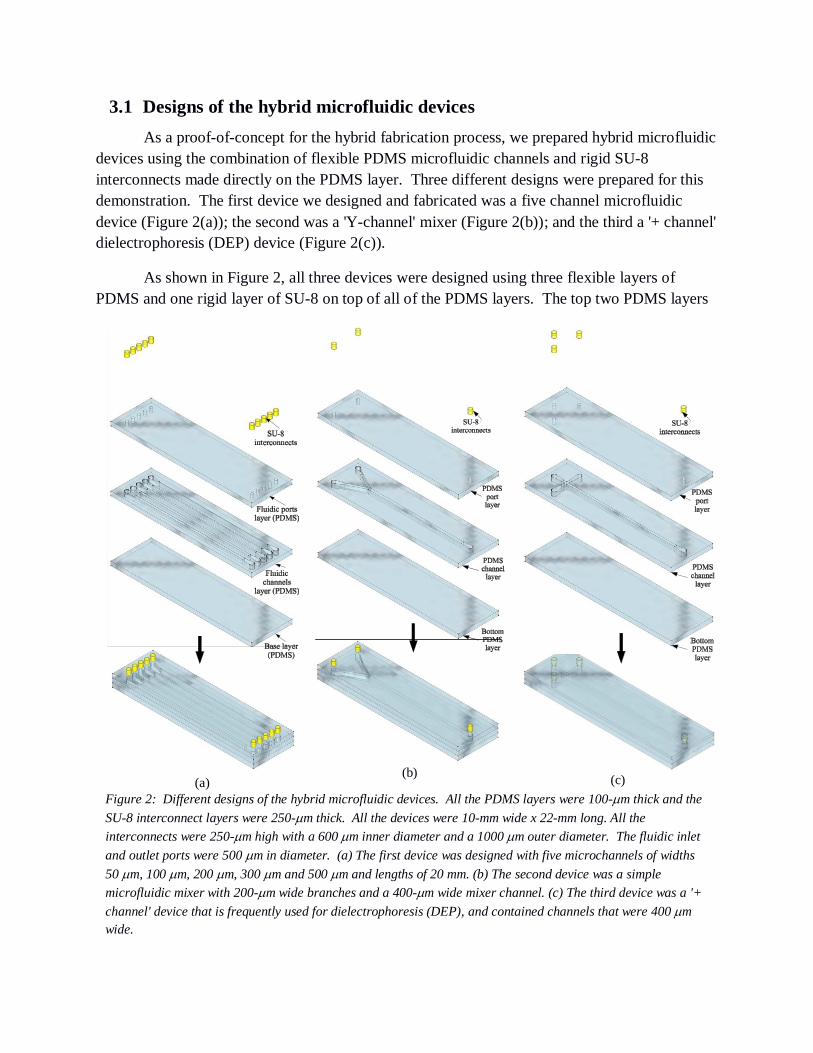
3.1 Designs of the hybrid microfluidic devices
As a proof-of-concept for the hybrid fabrication process, we prepared hybrid microfluidic
devices using the combination of flexible PDMS microfluidic channels and rigid SU-8
interconnects made directly on the PDMS layer. Three different designs were prepared for this
demonstration. The first device we designed and fabricated was a five channel microfluidic
device (Figure 2(a)); the second was a 'Y-channel' mixer (Figure 2(b)); and the third a '+ channel'
dielectrophoresis (DEP) device (Figure 2(c)).
As shown in Figure 2, all three devices were designed using three flexible layers of
PDMS and one rigid layer of SU-8 on top of all of the PDMS layers. The top two PDMS layers
(a)
(b)
(c)
Figure 2: Different designs of the hybrid microfluidic devices. All the PDMS layers were 100-m thick and the
SU-8 interconnect layers were 250-m thick. All the devices were 10-mm wide x 22-mm long. All the
interconnects were 250-m high with a 600 m inner diameter and a 1000 m outer diameter. The fluidic inlet
and outlet ports were 500 m in diameter. (a) The first device was designed with five microchannels of widths
50 m, 100 m, 200 m, 300 m and 500 m and lengths of 20 mm. (b) The second device was a simple
microfluidic mixer with 200-m wide branches and a 400-m wide mixer channel. (c) The third device was a '+
channel' device that is frequently used for dielectrophoresis (DEP), and contained channels that were 400 m
wide.

and the layer of SU-8 interconnects were prepared on the same substrate using a layer-by-layer
direct spin-on process to form the hybrid polymer stack. The bottom PDMS layer was prepared
on a separate substrate and bonded with the hybrid polymer stack using the oxygen plasma to
activate this interface [13][14].
The multilayer SU-8 mold for the PDMS channel (middle) layer and the PDMS fluidic
port (top) layer was prepared on a base substrate. Subsequently, the PDMS mixture was poured
and cured. Finally, the rigid SU-8 interconnect layer was directly processed onto the PDMS
layer when the PDMS layer was still on the mold. By using this layer-by-layer direct spin-on
approach, we were able to achieve accurate alignment of the features using a highly repeatable
fabrication process.
All the hybrid microfluidic devices had a base that was 10-mm wide and 22-mm long.
The first device (Figure 2(a)) consisted of different sized microfluidic channels, which were used
in the microfluidic pressurization test. The five different widths of these microchannels were 50
m, 100 m, 200 m, 300 m and 500 m. All these channels were 20 mm long. The second
device (Figure 2(b)) was a 'Y channel' microfluidic device generally used as a simple mixer of
two different types of fluids. Both the inlet branches were 200 m wide and the mixer channel
was 400 m wide. The third device (Figure 2(c)) was the '+ channel' device, which is often used
for dielectrophoresis (DEP) experiments. All the channels were 400 m wide in this DEP device.
The bottom PDMS layer was 500-m thick, the microchannel layer was 100-m thick
and the layer supporting the microfluidic ports was also 100-m thick. The microfluidic ports
were 500 m in diameter for all the devices. The SU-8 interconnect layers were 250-m high
with an inner diameter of 600 m and an outer diameter of 1000 m.
3.2 Detailed fabrication flow of the hybrid microfluidic device
In this section, the detailed flow is described for the fabrication process to create the
dielectrophoresis device. The same fabrication process flow, although using different
photolithography masks, was used to fabricate other two devices. In the end, photolithography
masks were also prepared that accommodated all the designs on a same substrate. As mentioned
earlier, the top two PDMS layers along with the SU-8 interconnect layer were processed on the
same substrate using the layer-by-layer self-registration process to obtain a reproducible
alignment between the processed layers. The procedures for the fabrication process to assemble
the hybrid microfluidic device are outlined in Figure 3.

To reliably process the SU-8 layers with different thicknesses, accurate process
Figure 3: The Step-by-step fabrication process for creating the hybrid microfluidic devices. (a) On a cleaned
glass substrate, a 100-m thick layer of SU-8 was spun and soft baked. (b) This soft baked SU-8 layer was
selectively exposed to UV irradiation through a photolithography mask designed for the mold of a microchannel.
(c) A second layer of 100-m thick SU-8 was directly spun onto the first layer of SU-8 and both layers were
baked using the appropriate parameters for soft bake of the second SU-8 layer. (d) Expose the second layer of
SU-8 to UV irradiation through a photolithography mask to define the inlet and outlet ports, followed by heating
for the post-exposure bake. (e) The uncrosslinked SU-8 was removed by rinsing these stacked layers in SU-8
developer, and these multiple layers of stacked SU-8 structures were hard baked. (f) The PDMS mixture was
prepared using Sylgard 184® elastomer and the appropriate curing agent kit. A mixture of both components was
poured over the multilayer SU-8 mold and cured at an elevated temperature. (g) The PDMS surfaces were
plasma treated and a 250-m thick SU-8 layer was spun coat directly onto these surfaces to make the rigid
interconnect structures. (h) After soft baking this SU-8 layer, it was exposed to UV irradiation through a
photolithography mask appropriate for patterning the interconnects. This assembly was heated for the post-
exposure bake, and (i) solvent developed to dissolve the unexposed (uncrosslinked) SU-8. (j) The hybrid polymer
stack was peeled away from the supporting substrate and bonded with the bottom PDMS piece by plasma
activation.

parameters for each fabrication step should be optimized. For the SU-8 fabrication process,
these steps consists of spin, softbake, UV exposure, post exposure bake, development and hard
bake. Similarly, for PDMS, these processing steps consist of mixing elastomer and curing agent,
degassing, pouring on to mold and curing. The parameters for the fabrication of the SU-8 and
PDMS layers used in these experiments were previously determined and reported in the literature
[11][12].
Using a clean glass substrate, a 100-m thick SU-8 layer was spun for the microchannels
mold (Figure 3(a)). The first SU-8 layer was heated on a hot plate and exposed to UV irradiation
through the photolithography mask for the appropriate microchannels (Figure 3(b)). A second
layer of 100-m thick SU-8 was spun onto the first layer of UV exposed SU-8 (Figure 3(c)).
The resulting stack of SU-8 was heated on a hot plate using the soft bake parameters of the
second SU-8 layer. Both of the SU-8 layers were subsequently exposed using the
photolithographic mask for microfluidic ports (Figure 3(d)). Subsequently, both the SU-8 layers
were heat treated on a hot plate for the post-exposure bake and rinsed extensively using the SU-8
developer (Figure 3(e)). The solvent developed stack of SU-8 layers was then rinsed with a fresh
portion of the SU-8 developer and followed with a rinse of isopropyl alcohol (IPA). The
resulting multilayer SU-8 molds were hard baked for the structural stability. These SU-8 molds
were subsequently used to make tri-layer structure of PDMS/PDMS/SU-8.
The PDMS mixture was prepared by mixing the Sylgard 184® elastomer and the curing
agent in 10:1 (w/w) ratio. The de-gassed mixture was poured onto the multilayer structure of
SU-8 and any excess amount of the uncured PDMS was scraped off from these molds. The
removal of the excess PDMS was an important step to achieve PDMS layers of the desired
thickness and upon which were created the microfluidic inlet and outlet ports. Additionally, the
scraping action also ensures that PDMS was removed from the tops of the mold for the
microfluidic ports and, hence, there remained clear openings to these ports after removal of the
PDMS from these SU-8 molds. The PDMS mixture cast against this mold was cured at an
elevated temperature (Figure 3(f)).
Now, the multilayer SU-8 molds and the PDMS stack is exposed with the oxygen plasma.
The polymer stack (the SU-8 molds and the PDMS layer) prepared on the glass substrate was
treated with the oxygen plasma. Right after the glass substrate with the polymer stack was
removed from the surface treatment, a 250-m thick SU-8 layer was spun onto the PDMS layer
to create the rigid interconnect structures (Figure 3(g)). The SU-8 layer was soft baked and
exposed to UV irradiation through the photolithography mask for creating the pattern of the
interconnect structures (Figure 3(h)). The UV exposed SU-8 layer was then heated for the post-
exposure bake and solvent developed using the SU-8 developer (Figure 3(i)).
The processed hybrid polymer stack of PDMS layers and the SU-8 interconnects were
gently peeled away from their molds. The bottom layer of PDMS within this hybrid stack was
bonded with a flat layer of PDMS, which was prepared separately, to seal the channels of the
hybrid microfluidic device (Figure 3(j)). The resulting hybrid microfluidic device was flexible
and included permanently bonded rigid SU-8 interconnects for chip-to-chip and/or world-to-
chip/chip-to-world interconnections.
The completed hybrid microfluidic devices were visually inspected and mechanically
tested for functionality and performance as discussed in the following section.
4 Experimental results & discussions
The fabrication process to make hybrid polymer-based flexible devices, including hybrid
microfluidic devices, was tested for different aspects during and after each of the fabrication
steps. An especially important component was the bond strength between the PDMS layer and
the SU-8 layer (the interconnects), which we tested many times during the technology
development. The completed PDMS and SU-8 based hybrid microfluidic device was also tested
with the microfluidic pressurization test to determine functionality of the interconnects for chip-
to-chip and/or world-to-chip/chip-to-world connections. Each experimental test along with the
results obtained from these test are discussed in the following sub-sections.
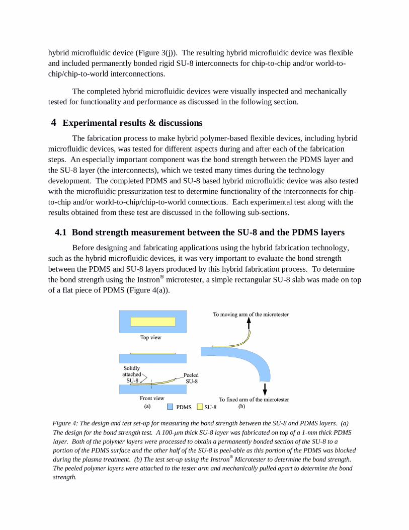
4.1 Bond strength measurement between the SU-8 and the PDMS layers
Before designing and fabricating applications using the hybrid fabrication technology,
such as the hybrid microfluidic devices, it was very important to evaluate the bond strength
between the PDMS and SU-8 layers produced by this hybrid fabrication process. To determine
the bond strength using the Instron® microtester, a simple rectangular SU-8 slab was made on top
of a flat piece of PDMS (Figure 4(a)).
Figure 4: The design and test set-up for measuring the bond strength between the SU-8 and PDMS layers. (a)
The design for the bond strength test. A 100-m thick SU-8 layer was fabricated on top of a 1-mm thick PDMS
layer. Both of the polymer layers were processed to obtain a permanently bonded section of the SU-8 to a
portion of the PDMS surface and the other half of the SU-8 is peel-able as this portion of the PDMS was blocked
during the plasma treatment. (b) The test set-up using the Instron® Microtester to determine the bond strength.
The peeled polymer layers were attached to the tester arm and mechanically pulled apart to determine the bond
strength.

The Instron® microtester is a mechanical tester capable of very accurate displacement and
includes a PC-based measurement system. The test samples were attached to the top and the
bottom arms of the tester and mechanically pulled apart while measuring the respective force.
To be accommodated in this test set-up, the PDMS and the SU-8 based test structures were
fabricated specifically to attach securely into the grippers of the top and the bottom arms (Figure
4(a)). To obtain such structures, a portion of the PDMS layer was covered with a piece of glass
during the surface treatment. Hence, one-half of the subsequently processed SU-8 layer was
permanently bonded to the PDMS layer and the other half of the SU-8 layer was easily peel-able
from the PDMS layer (this technology is explained in [11][12]).
After fabrication of the test structures, the SU-8 layer from the untreated PDMS area was
peeled-off and securely attached into the mechanical tester (Figure 4(b)). The PDMS layer was
attached to the fixed (bottom) arm of the microtester and the peeled SU-8 layer was attached to
the movable (top) arm of the microtester. Both the arms of the microtester were moved using the
defined linear displacement and the respective force was measured during this process.
After more than 20 measurements of different samples, it was clear that the PDMS layer
fails and ruptures every time without damaging the bond between the PDMS and the SU-8 layers
(Figure 5). The bond between the two polymers was intact in all the samples at the end of the
measurement. It is clear that the bond between the two polymers is strong and it isn't possible to
separate the polymer layers.
4.2 Fabrication related results
During the fabrication of the PDMS and SU-8 based hybrid microfluidic device, optical
microscopy images were captured using the optical microscope (Olympus MX40) to check
acceptability of the processed features after each step. Some of the important optical images are
included here (Figure 6 to Figure 9).
Figure 5: The bond test structure after the test in the Instron
® microtester. The PDMS layer is failed right next
to the joint of the PDMS and the SU-8 interface. The 100 m thick SU-8 layer onto the PDMS base layer is
clearly visible with half of the SU-8 rectangle permanently bonded on the PDMS.

In Figure 6, a high magnification image is shown for the multilayer SU-8 molds. The
final components within the mold were precisely aligned and clearly defined after the hard bake
step because of the layer-by-layer direct spin-on process. The molds in the image also adhered
very well to the glass substrate. A very uniform and consistent fabrication process was achieved
because of the precisely tuned parameters for a wide variety of the substrate materials [11][12].
Figures 7, 8 and 9 show the hybrid polymer stacks after the fabrication process was
completed on the substrate and while the stacked structure was still on the glass substrate. The
precisely aligned and permanently bonded SU-8 interconnects are clearly visible in all three
images. The accuracy of the alignment because of the layer-by-layer direct spin-on process is
Figure 6: Microscopic image of the multilayer SU-8
molds. The bottom SU-8 layer was defined for the
microchannels mold and the bottom SU-8 layer was
patterned for the fluidic ports. The multilayer SU-8
layer-by-layer process provided precise alignment of
the mold features.
Figure 7: Image of the hybrid polymer stack on a
square glass substrate. The hybrid polymer stack
consisted of the microchannel mold, the microfluidic
port mold, the PDMS channel and port, and the
patterned SU-8 interconnects. Additionally, all the
designs of the hybrid microfluidic devices were
included in the same design and hence on the same
substrate.
Figure 8: The high magnification image of the hybrid
polymer stack. The alignment and clear definition of
all the features are visible in the image.
Figure 9: A high magnification image of the hybrid
polymer stack. Precisely aligned and clearly defined
layers, such as the channel mold layer, the port mold
layer, the PDMS layer and the SU-8 interconnect are
visible.

clearly visible from the high magnification image of Figure 9. Additionally, consistency of the
processed layers throughout the substrate was excellent even after multilayer hybrid fabrication
process (Figure 7).
The optical microscope images clearly showed that the hybrid polymer fabrication
process using multilayer processing helps to produce uniform, well-defined, and reproducible
features. Additionally, the self-registration process for the multi-layer fabrication was able to
provide high accuracy in the layer-to-layer alignment.
4.3 Interconnect adhesion test
After the polymer-based hybrid microfluidic device was fabricated, the bond strength
between the SU-8 interconnects and the top PDMS layer was once again tested using the voice
coil actuator (VCA) as described in [11]. The graphical presentation of the test set-up is shown
in Figure 10.
In the VCA-based test set-up (Figure 10), a needle was attached to the VCA and the
pointed end of the needle was aligned to the SU-8 interconnect of the hybrid microfluidic device.
Force applied to the interconnects were in an attempt to use the VCA to detach these SU-8
structures from the top PDMS layer (the PDMS port layer). The force generated through the
VCA is linearly proportional to the current supplied to the VCA [11].
Using the VCA-based adhesion test, it was not possible to detach the SU-8 interconnects
from the PDMS layer. During all the tests, the SU-8 interconnects deformed the PDMS substrate
and moved away from the needle point. The acquired analytic data was, therefore, due to the
strong adhesion between the PDMS layer and the SU-8 interconnect.
Figure 10: The graphical presentation of the test set-up for the interconnect adhesion test using the voice coil
actuator (VCA). The fabricated hybrid microfluidic device was placed on a glass substrate and the needle
attached to the VCA was used to push the SU-8 interconnects, trying to remove them from the PDMS layer. In
all the tests, however, the SU-8 interconnect slipped from the needle because of the flexibility of the PDMS
layers.

4.4 Microfluidic test
After complete fabrication of the hybrid microfluidic devices, a microfluidic test was
performed on each of the devices to test their desired functionality. It was also important to
verify reliable completion of the process and absence of leakage in each of the devices. One of
the microscopic images of the microfluidic functionality test is shown here (Figure 11). The 'Y-
channel' device (Figure 2(c)) was injected with two separate solutions of de-ionized (DI) water
each containing a different dye molecule with a unique color (Figure 11).
During the microfluidic testing the devices were directly connected to the syringe pump
with Tygon®
tubing placed over the rigid SU-8 interconnects (Figure 11). The functional test of
these devices was performed using a flow rate of 0.05 mL/min created using a syringe pump
(Harvard Apparatus '11'). As shown in Figure 11, there was no leakage in these hybrid
microfluidic devices around interconnections, as well as from any other layer within these
devices. The lack of leaks was partially attributed to the design of each interconnect. The outer
diameter of each interconnect was slightly larger than the inner diameter of the Tygon®
tubing
(importance of this was explored in detail within [16]).
Besides the microfluidic functional test of the hybrid microfluidic devices, we also
performed a microfluidic pressurization test of the devices. For the microfluidic pressurization
test, a microfluidic device was used that contained different channel widths (Figure 2(a)). The
microfluidic test set-up was prepared using the syringe pump and a pressure sensor (Omega
PX26-005GV and Omega PX26-030GV) [11]. All the pressurization experiments were
Figure 11: Microfluidic testing of the 'Y-channel' mixer. The Tygon® tube was directly connected to the rigid
SU-8 interconnect without any leakage. DI water mixed with two different colors was injected in the inlet ports
of the mixer.

performed at a flow rate from 0.01 mL/min to 0.10 mL/min on three separate devices. The
determination of the leakage pressure was performed using the 50-m wide channels with a flow
rate from 0.01mL/min until leakage of the pumping fluid was observed under the optical
microscope. The simulation results obtained from COMSOL are used as a base line to select the
flow rates for each pressurization test. The simulation results along with the experimental
measurements from three different devices are plotted in Figure 12.
As shown in Figure 12, the microfluidic pressurization results are plotted in two parts.
The upper half of the plot represents the pressurization test results obtained from the simulation
and from the experimental measurements for the 100-m, 200-m, 300-m and 500-m wide
channels. As mentioned above, these tests were performed from flow rates of 0.01 mL/min to
Figure 12: Plot of the microfluidic pressurization test results of the COMSOL simulation and the experimental
measurements of the hybrid microfluidic device with 50-m, 100-m, 200-m, 300-m and 500-m wide
channels. The channels of widths100 m, 200 m, 300 m and 500 m were tested from 0.01 mL/min to 0.10
mL/min flow rate (top most plot) and the 50-m wide channel was tested until leakage was observed from the
microfluidic channels (bottom plot). The 50-m wide channel leaked at 85.85 kPa pressure at a flow rate of
0.20 mL/min.

0.10 mL/min. Similarly, the bottom half of the plot represents the pressurization test results and
simulation associated with the 50-m wide channels. As shown in Figure 12, the pressure in all
the microfluidic channels increased linearly with the flow rate. Additionally, none of the
channels leaked at flow rates up to 0.10 mL/min in all three devices. Another important aspect
for avoiding leakage and repeatable pressure responses was consistency of the feature size,
which is also visible from the plots in Figure 12. The repeatable results from the different
devices indicated repeatable alignment of the features in all the experiments.
Similarly, for the leakage pressure measurements using the 50-m wide channels,
channels were used from three different devices. In all three devices, the leakage between the
Tygon® tubing and the rigid SU-8 interconnect is observed when the flow rate is increased to 0.2
mL/min. The average pressure at which these three devices failed was 85.85 ± 3.56 kPa. Errors
were calculated from the standard deviation of three independent measurements.
The hybrid fabrication technology developed using the PDMS and the SU-8 materials
was very useful for fabricating hybrid microfluidic devices that can be modularly used for many
biomedical and microfluidic applications. The SU-8 interconnects provided easy chip-to-chip
and/or world-to-chip/chip-to-world interconnections without requiring any gaskets or special set-
ups. This modularity is especially useful for the biomedical devices that require polymer-based
disposable sub-systems.
5 Conclusions
A hybrid fabrication technology using the flexible polymer (PDMS) and the rigid
polymer (SU-8) is successfully presented in this article. A permanent bond between the flexible
and rigid polymer layers is achieved using oxygen plasma treatment of the PDMS followed by a
direct spin-on process to create the SU-8 features. Additionally, very accurate alignment and a
reliable process are achieved because of the layer-by-layer processing and the direct spin-on SU-
8 process on top of the PDMS layer.
To prove the usability of the hybrid fabrication technology, we developed hybrid
microfluidic devices with rigid interconnects. The fabrication technology is, however, not
limited to only this application, it can be utilized to develop many sophisticated microfluidic and
biomedical applications using these low cost polymers. Three different designs of the hybrid
microfluidic device were fabricated and tested.
From the adhesion tests between the two polymer layers, we conclude that the bond
strength between the two polymer layers is extremely strong. Because of such a strong bond, the
integrity of the PDMS material failed while the bond between the two polymer layers remained
intact during all experiments. This proof of permanent bond was also tested using different test
set-ups at different stages of the technology development.

The microfluidic test performed on the hybrid microfluidic devices proved modularity of
the rigid SU-8 interconnects for the world-to-chip/chip-to-world interconnections. The
microfluidic pressurization test performed on all the devices demonstrated a linear response to
pressure with respect to flow rates from 0.01 mL/min to 0.10 mL/min. The experimental test
response obtained from three different devices also demonstrated the precise alignment achieved
in this process and the repeatable process yield. The 50-m wide channels of the hybrid
microfluidic devices leaked upon reaching a flow rate of 0.20 mL/min and a pressure of 85.85 ±
3.56 kPa.
6 References
1. Jo B H, Van Lerberghe L M, Motsegood K M and Beebe D J 2000 Three-dimensional
micro-channel fabrication in polydimethylsiloxane (PDMS) elastomer J.
Microelectromech. Syst. 9 76–81
2. Unger M A, Chou H P, Thorsen T, Scherer A and Quake S R 2000 Monolithic
microfabricated valves and pumps by multilayer soft lithography Science 288 113–6
3. Neils C, Tyree Z, Finlayson B and Folch A 2004 Combinatorial mixing of microfluidic
streaks Lab Chip 4 342–50
4. Foulds I G and Parameswaran M 2006 A planar self-sacrificial multilayer SU-8-based
MEMS process utilizing a UV-blocking layer for the creation of freely moving parts J.
Micromech. Microeng. 16 2109-15
5. Belanger M-C and Marois Y 2001 Hemocompatibility, Biocompatibility, Inflammatory
and in Vivo Studies of Primary Reference Materials Low-Density Polyethylene and
Polydimethylsiloxane: A Review Journal of Biomedical materials 58 (5) 467 – 77
6. Schoning M J, Jacobs M, Muck A, Knobbe D-T, Wang J, Chatrathi M and Spillmann S
2004 Amperometric PDMS/glass capillary electrophoresis-based biosensor microchip for
catechol and dopamine detection Sensors and Actuators B 108 688 – 94
7. Chang W J, Akin D, Sedlak M, Ladisch M R and Bashir R 2003 Poly(dimethylsiloxane)
(PDMS) and Silicon Hybrid Biochip for Bacterial Culture Biomedical Microdevices 5(4)
281 – 90
8. Tang L and Lee N Y 2010 A facile route for irreversible bonding of plastic-PDMS hybrid
microdevices at room temperature Lab on a Chip 10 1274 – 80
9. Westwood S M, Jaffer S and Gray B L 2008 Enclosed SU-8 and PDMS microchannels
with intergrated interconnects for chip-to-chip and world-to-chip connections J.
Micromech. Microeng. 18 064014 (9 pp)

10. Xia Y and Whitesides M 1998 Soft Lithography Annu. Rev. Mater. Sci. 28 153 – 84.
11. Patel J N, Kaminska B, Gray B L and Gates B D 2008 PDMS as a sacrificial substrate for
SU-8-based biomedical and microfluidic applications J. Micromech. Microeng. 18
095028 (11 pp)
12. Patel J N, Kaminska B, Gray B L and Gates B D 2009 A sacrificial SU-8 mask for direct
metallization on PDMS J. Micromech. Microeng. 19 115014 (10 pp)
13. Bhattacharya S, Datta A, Berg J M and Gangopadhyay S 2005 Studies on Surface
Wettability of Poly(Dimethyl) Siloxane (PDMS) and Glass Under Oxygen-Plasma
Treatment and Correlation With Bond Strength Journal of Microelectromechanical
Systems 14 (3) 590 – 97
14. Owen M J and Smith P J 1994 Plasma treatment of polydimethylsiloxane Journal of
Adhesion Science and Technology 8(10) 1063 – 75
15. Blanco F J, Agirregabiria M, Garcia J, Berganzo J, Tijero M, Arroyo M T, Ruano J M,
Aramburu I and Mayora K 2004 Novel three-dimensional embedded SU-8 microchannels
fabricated using a low temperature full wafer adhesive bonding J. Micromech. Microeng.
14 1047 – 56
16. Jaffer S and Gray B L 2008 Polymer mechanically interlocking structures as
interconnects for microfluidic systems J. Micromech. Microeng. 18 035043 (10 pp)


![Fabrication of PDMS micro through-holes for ... · SeveralattemptshavebeenmadetofabricatePDMSmicro through-holelayers.Parketal.[17] developed a simple meth-od for fabricating a PDMS](https://img.pdfslide.us/doc/110x75/5b0afd8e7f8b9ac7678d4f52/fabrication-of-pdms-micro-through-holes-for-through-holelayersparketal17.jpg)
![Fabrication and transfer of fragile 3D PDMS microstructures527942/... · 2015. 9. 29. · bonding [2], PDMS has unique properties difficult to obtain with other materials. An example](https://img.pdfslide.us/doc/110x75/6138a96a0ad5d20676496515/fabrication-and-transfer-of-fragile-3d-pdms-microstructures-527942-2015-9.jpg)