Embed Size (px)
Citation preview
Studying Thermal Management for Graphics-Processor Architectures
Jeremy W. Sheaffer, Kevin Skadron, David P. LuebkeDepartment of Computer Science
The University of Virginia{jws9c, skadron, luebke}@cs.virginia.edu
Abstract
We have previously presented Qsilver, a flexible sim-ulation system for graphics architectures. In this paperwe describe our extensions to this system, which we use—instrumented with a power model and HotSpot—to analyzethe application of standard CPU static and runtime ther-mal management techniques on the GPU. We describe ex-periments implementing clock gating, fetch gating, dynamicvoltage scaling, multiple clock domains and permuted floor-planning on the GPU using our simulation environment,and demonstrate that these techniques are beneficial in theGPU domain. Further, we show that the inherent paral-lelism of GPU workloads enables significant thermal gainson chips designed employing static floorplan repartitioning.
1 Introduction
Commodity graphics hardware is evolving at a tremen-dous rate, with each successive generation adding not onlyperformance but fundamentally new functionality. Graphicsprocessors (GPUs) sport sophisticated memory hierarchies,multiple issue, wide parallel SIMD and MIMD pipelines,and NVIDIA’s current offering, the “NV40” architecture,implements out-of-order issue [15].
Graphics architectures are also becoming more pro-grammable, with greater program sophistication possiblewith each generation. Early programmable GPUs had pro-grammability available only in the vertex engine, they werelimited with respect to size of programs, and these pro-grams could not have branch instructions. More recent gen-erations have added conditional expressions, the ability toexecute much larger programs, and the ability to programthe pixel engine. The current generation of hardware evensupports fully general branching (loops, subroutines, etc.).As these processors continue to add programmability, theybecome more general. GPUs offer very high performancein their specialized domain; with massively parallel float-ing point arrays and the recent trends toward increased pro-
grammability, they are beginning to be applied towards sci-entific computing. Such applications of graphics hardwareare known within the graphics community as GPGPU, shortfor General Purpose Graphics Processing Unit.
The rapid rate of innovation in graphics architecture,combined with the need for energy and thermal effi-ciency, creates a rich design space well-suited for studyby the methods familiar to the general-purpose processor-architecture community. Yet the inherent parallelism ofGPU workloads makes the design space much richer thanfor traditional CPUs, and the lack of a suitable publicly-available simulation infrastructure has hampered academicresearch in GPU architecture. The lack of infrastructure isparticularly serious, since in the time required to build acomplex simulation infrastructure, the simulated architec-ture can easily become obsolete. GPU architectures alsospan a wide range of aggressiveness, from high-end prod-ucts intended for gaming and scientific visualization, wherethe emphasis is on performance, to low-end products formobile applications, where the emphasis is on energy effi-ciency.
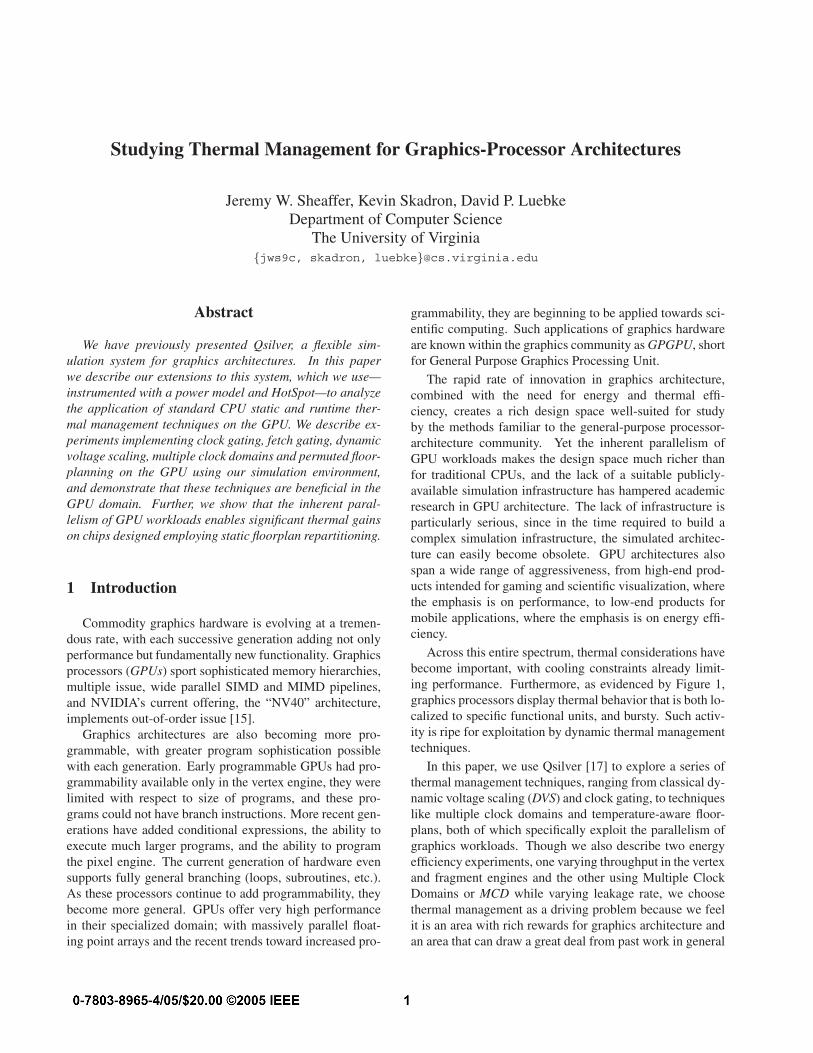
Across this entire spectrum, thermal considerations havebecome important, with cooling constraints already limit-ing performance. Furthermore, as evidenced by Figure 1,graphics processors display thermal behavior that is both lo-calized to specific functional units, and bursty. Such activ-ity is ripe for exploitation by dynamic thermal managementtechniques.
In this paper, we use Qsilver [17] to explore a series ofthermal management techniques, ranging from classical dy-namic voltage scaling (DVS) and clock gating, to techniqueslike multiple clock domains and temperature-aware floor-plans, both of which specifically exploit the parallelism ofgraphics workloads. Though we also describe two energyefficiency experiments, one varying throughput in the vertexand fragment engines and the other using Multiple ClockDomains or MCD while varying leakage rate, we choosethermal management as a driving problem because we feelit is an area with rich rewards for graphics architecture andan area that can draw a great deal from past work in general
92
94
96
98
100
102
104
106
108
0 0.5 1 1.5 2 2.5 3 3.5
Te
mp
era
ture
(C
)
Time (s)
Temperature Variation over Time for 100 Frames
Vertex EngineFragment Engine
Figure 1. The temperature variation on thechip is both localized, at the granularity ofthe functional unit block, and bursty. Thesetraces plot temperature over time process-ing an execution trace on a system basedon the base low-resolution floorplan (see Fig-ure 3). It is also evident that the GPU dis-plays both inter- and intra-frame variations inactivity and temperature fluctuation. The fre-quent periodic variations correlate to individ-ual frames.
purpose processor design. Furthermore, and perhaps moreimportantly, we believe that these two communities—thoseof general purpose and of graphics processor architects—have much to offer each other. We hope that our work willspur interest that leads to cross fertilization of ideas betweenthese largely disjoint groups.
2 Related Work: Architectural Simulation
The advent of detailed but flexible, configurable, cycle-accurate CPU simulators in the 1990s for complex, super-scalar architectures served as the catalyst for an explosionof quantitative research in the computer architecture com-munity. The most prevalent simulator in academic archi-tectural research is SimpleScalar [2]; other simulators usedin specific circumstances include Rsim [6] for multipro-cessors, as well as Simics [9] and SimOS [14] for captur-ing operating-system and multi-programmed behavior. Bydescribing instruction flow at the granularity of individualsteps through the CPU pipeline, these simulators allowedresearch and design to move beyond good but impreciseanalytical models or cumbersome, logic-level models. In-stead, architects could analyze detailed tradeoffs under re-
alistic workloads and estimate how various microarchitec-tural choices affected instruction throughput. Examples ofproblems that can now be studied at least partially thanks toacademic architectural simulators include the impact of dif-ferent cache and branch predictor algorithms, the impact ofdifferent superscalar out-of-order instruction-issue designs,and the effectiveness of a host of novel CPU organizationssuch as hyper-threading.
These simulation systems are not alone; new infrastruc-tures continue to appear. One of these, ASIM [11], offers ahigh degree of flexibility in definition of the system beingsimulated. It is much like Qsilver in this respect. UnlikeQsilver, ASIM uses an asynchronous event model for com-munication between blocks, while QSilver, being designedwith the GPU in mind, depends on a streaming infrastruc-ture and more conventional intra-block communication.
More recently, power-modeling capability launched an-other round of innovation by allowing architects to estimatethe energy efficiency of different processor organizations,verify that new microarchitecture innovations are justifiablefrom an energy-efficiency standpoint, and explore microar-chitectural techniques for managing energy efficiency. Thedominant power model today is Wattch [3], which uses cal-ibrated analytical models to allow flexible and configurableestimation of power for a variety of structures, structuresizes, organizations, and semiconductor technology gen-erations or nodes. Other power models that use circuit-extracted data have been described, but they are basedon specific implementations and tend to be less flexible.These two approaches can be combined, using the circuit-extracted model as calibration for Wattch’s analytical mod-els; see for example a recent study of hyper-threading us-ing IBM’s circuit-extracted PowerTimer [8]. Most recently,the architecture community has begun to explore architec-tural techniques for thermal management, facilitated by theHotSpot [20] dynamic temperature model. This paper ex-tends our earlier work in thermally aware graphics proces-sor design [18].
Our goals with Qsilver are to stimulate the same kindof innovation in the GPU community that products such asSimpleScalar have stimulated in the general purpose archi-tecture community, to stimulate greater cross-fertilizationof ideas with the general-purpose CPU architecture com-munity, and to enable new studies in power-aware andtemperature-aware design.
3 Description and Modification of the Simu-lator
3.1 Description of Qsilver
There are two major components of the Qsilver system:the annotator and the simulator core. The annotator gener-
ates an input trace, which the simulator core traces throughits cycle timer model. This section summarizes Qsilver aspresented in [17].
3.1.1 The Annotator
The Qsilver annotator is built on Chromium [7], an OpenGLlibrary interceptor which implements and exports theOpenGL API, an API for realtime 3D graphics. Chromiumallows the OpenGL call stream of an application to be in-tercepted and transformed on the fly, without need of anymodification or source code. Chromium is typically usedfor such applications as scientific simulation and visualiza-tion; for example, splitting output over multiple displays orbalancing a graphics workload over many GPUs. By im-plementing several new Chromium stream processing units(SPUs), we transform the OpenGL stream in such a waythat we can gather aggregate statistics about the activitiesof the hardware during rendering. These statistics form theinput to our cycle-timer simulation.
An unfortunate fault of our Chromium based annota-tor is our inability to gather non-aggregate data, specifi-cally screen-space positional information and texture coor-dinates. Many structures, such as the texture cache, cannotbe accurately modeled with the current system. Another av-enue worth exploring as a base system for the Qsilver anno-tator is the use of a software renderer like Mesa [12]. WithMesa, we would sacrifice some of the speed of the currentsystem, and in exchange get all of the current functionality,as well as the non-aggregate data required for lower levelsimulation. We intend to move the annotator to Mesa, orsome Chromium/Mesa hybrid, in our future work.
Video games drive the graphics hardware market; how-ever many games will not run if they cannot maintain suf-ficient framerate. Since our annotation system significantlyslows the annotated application, we also use Chromium torecord and play back an OpenGL trace of the application.This trace is no longer the application itself, but only itscalls into the OpenGL API. As the application logic has al-ready been processed, framerate is no longer a concern. Wepass this OpenGL trace to the annotator for data aggrega-tion.
The annotation process consists of the following stages,implemented as Chromium SPUs:
1. Expansion of vertex arrays
OpenGL allows vertices to be specified in two mainways: individually, with component parameters spec-ified explicitly in the call, and as part of a set of ver-tices stored in an array on the GPU and indexed by anelement number. For efficiency reasons, and becauseonly a single call in to the API is required to rendercomplex geometries, the latter, called a vertex array or
vertex buffer, is favored by game developers. As de-scribed below, we need all geometry to be broken intoindividual triangles, so the first task of the annotatoris to expand the vertex arrays to produce the triangleswhich will eventually pass through to the GPU. Themost significant problem with complex geometries isthat they can be self occluding. The first three SPUs inour SPU chain are designed to eliminate self occlusion.Also note that to correctly model such structures as thevertex cache, it is necessary to maintain an awarenessof the original layout of the vertex array.
2. Unfolding of display lists
Display lists are another efficiency construct of theOpenGL API. Like vertex arrays, display lists allowscomplex geometries to be rendered with a single APIcall. We use Chromium to store display lists as they are‘recorded’, then monitor the stream for the API callswhich play them back. When the call comes through,we play back the recorded source rather than passingthe display list invocation though to the driver.
3. Triangulation of geometries
The GPU deals with geometry in terms of individualtriangles, but OpenGL allows specification of geome-try in terms of triangle strips and fans, and polygonswith an arbitrary number of sides. These complex ge-ometries need to be triangulated—turned in to indi-vidual triangles—before they can be rasterized. Thisstage of the annotator further transforms the OpenGLcall stream such that subsequent stages receive onlytriangulated geometry.
4. Query of state and activity
Rasterization is the process of turning triangles intofragments, which can be thought of as a generaliza-tion of pixels. The transformations leading to this stageeliminate complex geometry—meaning that all geom-etry coming to this stage is organized into individ-ual triangles—and with them self occlusion. In orderto accurately model a GPU, we must know—amongother statistics—how many fragments were generatedfrom a triangle and how many of these fragments passthe depth test and get written to the framebuffer. Wewrap each triangle in an occlusion query which returnsa count of the number of non-occluded fragments thatthat triangle generates on the hardware. We then ren-der the triangle again into another buffer with the depthtest disabled, wrapped in another occlusion query, todetermine the total number of fragments generated bythe triangle.
In addition to counting fragments, in this stage we alsocollect some information on OpenGL state and count
statistics such as the number of texture accesses inthis stage. The latter is non-trivial, as magnificationand minification texture sampling filters do not nec-essarily make the same number of texel accesses, andit requires some further manipulation of the OpenGLstream, another rendering of the triangle in question,another occlusion query, and use of the programmablefeatures of modern GPUs. For full details, please see[17].
The annotator ultimately writes an annotated trace todisk. This trace describes what the hardware must do torender the OpenGL trace input. The simulator core takesthis annotated trace as input for its timing simulation.
3.1.2 The Simulator Core
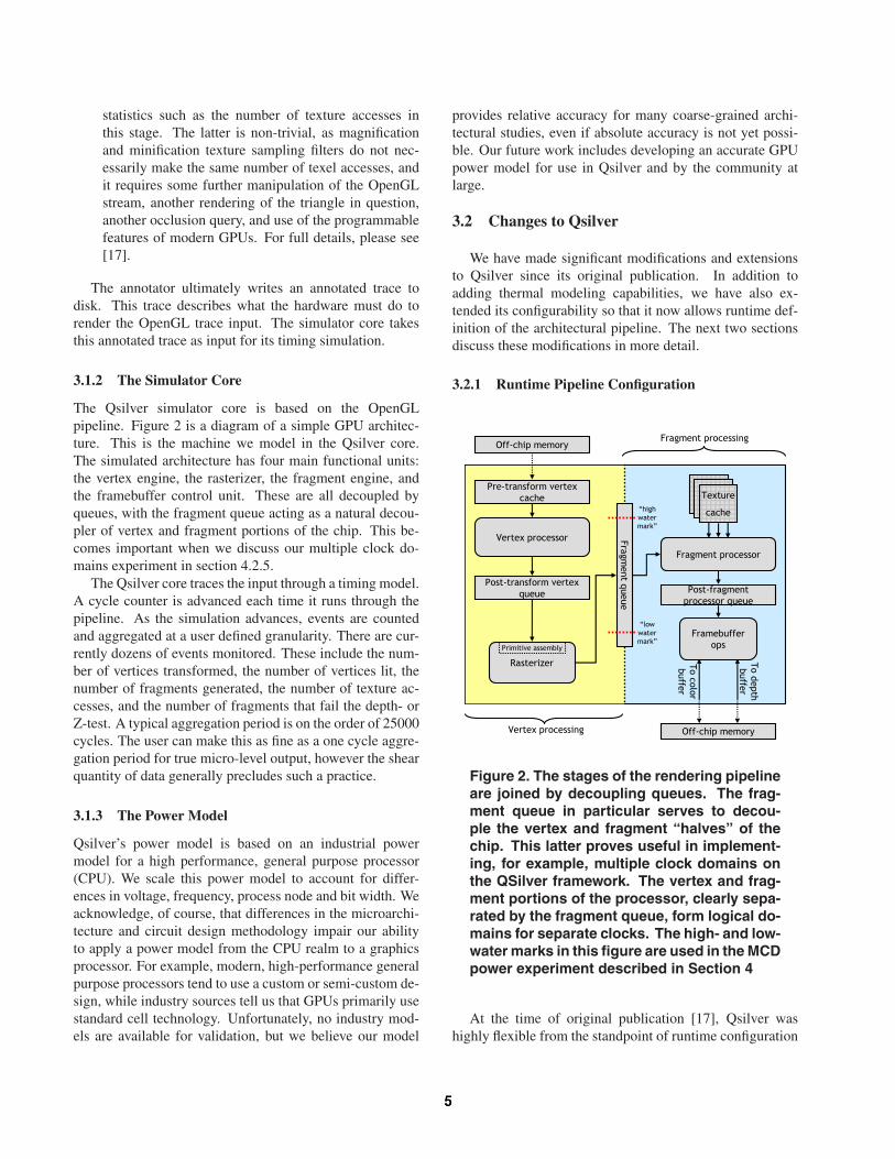
The Qsilver simulator core is based on the OpenGLpipeline. Figure 2 is a diagram of a simple GPU architec-ture. This is the machine we model in the Qsilver core.The simulated architecture has four main functional units:the vertex engine, the rasterizer, the fragment engine, andthe framebuffer control unit. These are all decoupled byqueues, with the fragment queue acting as a natural decou-pler of vertex and fragment portions of the chip. This be-comes important when we discuss our multiple clock do-mains experiment in section 4.2.5.
The Qsilver core traces the input through a timing model.A cycle counter is advanced each time it runs through thepipeline. As the simulation advances, events are countedand aggregated at a user defined granularity. There are cur-rently dozens of events monitored. These include the num-ber of vertices transformed, the number of vertices lit, thenumber of fragments generated, the number of texture ac-cesses, and the number of fragments that fail the depth- orZ-test. A typical aggregation period is on the order of 25000cycles. The user can make this as fine as a one cycle aggre-gation period for true micro-level output, however the shearquantity of data generally precludes such a practice.
3.1.3 The Power Model
Qsilver’s power model is based on an industrial powermodel for a high performance, general purpose processor(CPU). We scale this power model to account for differ-ences in voltage, frequency, process node and bit width. Weacknowledge, of course, that differences in the microarchi-tecture and circuit design methodology impair our abilityto apply a power model from the CPU realm to a graphicsprocessor. For example, modern, high-performance generalpurpose processors tend to use a custom or semi-custom de-sign, while industry sources tell us that GPUs primarily usestandard cell technology. Unfortunately, no industry mod-els are available for validation, but we believe our model
provides relative accuracy for many coarse-grained archi-tectural studies, even if absolute accuracy is not yet possi-ble. Our future work includes developing an accurate GPUpower model for use in Qsilver and by the community atlarge.
3.2 Changes to Qsilver
We have made significant modifications and extensionsto Qsilver since its original publication. In addition toadding thermal modeling capabilities, we have also ex-tended its configurability so that it now allows runtime def-inition of the architectural pipeline. The next two sectionsdiscuss these modifications in more detail.
3.2.1 Runtime Pipeline Configuration
To depth buffer
Pre-transform vertex cache
Off-chip memory
Vertex processor
Post-transform vertex queue
Rasterizer
Fragment queue
Fragment processor
Texture
cache
Post-fragment processor queue
Framebuffer ops
To color buffer
Primitive assembly
Off-chip memoryVertex processing
Fragment processing
“lowwatermark”
“highwatermark”
Figure 2. The stages of the rendering pipelineare joined by decoupling queues. The frag-ment queue in particular serves to decou-ple the vertex and fragment “halves” of thechip. This latter proves useful in implement-ing, for example, multiple clock domains onthe QSilver framework. The vertex and frag-ment portions of the processor, clearly sepa-rated by the fragment queue, form logical do-mains for separate clocks. The high- and low-water marks in this figure are used in the MCDpower experiment described in Section 4
At the time of original publication [17], Qsilver washighly flexible from the standpoint of runtime configuration
of state variables. We could, at runtime, define such param-eters as the number of pipelines in the fragment core, thelength of the vertex queue, or the bandwidth of the networkbetween the fragment queue and fragment engine. A ma-jor failing was the inability to define the simulated pipelineitself at runtime.
We undertook a complete rewrite of the Qsilver system.The changes to the annotator are mostly cosmetic, but thechanges to the simulator core itself are significant. The mostimportant modification is our addition of runtime pipelineconfiguration.
Qsilver now is essentially a stream system. The userwrites kernels, in the form of C functions, representing eachstage of the pipeline they wish to simulate (of course theyalso may use an existing kernel). The stream infrastructuresees that the kernels receive input, and it is the responsibil-ity of the pipeline builder to signal the infrastructure whenwork is complete on a particular datum. This is similar tothe approach that was used in the Liberty system [21].
At runtime, the pipeline itself is organized into a list offunction pointers. The simulation infrastructure traversesthe list and calls each function or kernel with its associatedinput and a state data structure that is also stored in the list.With this organization, it is straightforward to run multiplesimulations, each using a different pipeline configuration,without need for a recompile. Configuration of the pipeline,as well as all runtime state variables, is handled in a single,simple configuration file.
3.2.2 Thermal Modeling with HotSpot
We have augmented Qsilver with HotSpot [5, 19], a tool forarchitectural thermal modeling. Drawing from the powermodel described in section 3.1.3 and based on the floorplansin section 4.2.1, HotSpot is invoked at the end of every ag-gregation period to calculate the temperature of each func-tional unit.
HotSpot builds a system of differential equations whichdescribe a complex RC circuit—conveniently thermal sys-tems are modeled in exactly the same way as electrical RCcircuits, with a thermal resistance and capacitance—andsolves them numerically for temperatures.
4 Experiments and Results
Figure 1 is a trace of the thermal activity of the vertexengine and the framebuffer control unit over 100 frames ofdata. From this plot, we can see that thermal activity isboth localized and bursty. The dynamic thermal manage-ment techniques discussed below capitalize on this charac-teristic.
Given the limitations of our power model combined withthe dependence of temperature on power, and the fact that
we have not fully explored the design space for any of thesetechniques, we must acknowledge that the ‘error bars’ onour results are large. Without a more accurate power model,we cannot precisely, quantitatively compare the techniqueslisted below. Nonetheless, we reiterate that we believe ourresults hold qualitatively, and that interesting insights can begained from this work. As a case in point, below we showthat DVS outperforms MCD with respect to performance inmanaging temperature on the GPU. This is consistent withthe literature, but with our large and unquantified error, thesmall difference in performance of these techniques, and thefact that MCD does a better job of controlling temperature,we should probably consider these techniques to be in anequivalence class! Both present interesting room for furtherstudy.
4.1 Experiments
On top of the QSilver framework we implemented thefollowing thermal management techniques:
• Global Clock Gating
This technique stops the clock when any monitoredunit on the chip exceeds a threshold temperature. Theclock is restarted when the temperature of all the unitsis once again below the threshold. With this tech-nique, the processor is effectively turned off wheneverthe chip experiences thermal stress, except that state ispreserved and leakage currents are unaffected.
• Fetch Gating
Fetch gating, in a general purpose processor, toggleson and off the instruction fetch stage of the pipeline,effectively reducing the throughput of the entire pipe.Due to the decoupled nature of the rendering pipeline,we believe that this technique can be used effectivelyin any stage of the pipeline. We have tested it, withpositive results, on the vertex fetch and transform-and-light (another name for the vertex engine) stages.
• Dynamic Voltage Scaling
In Dynamic Voltage Scaling, or DVS, voltage is re-duced upon crossing the thermal threshold. With lowervoltage, the switching speed of the transistors is de-creased, so it is necessary to also scale frequency. Be-cause P ∝ V 2f , this technique achieves a roughly cu-bic reduction in power relative to performance loss1.Employing this technique, the power saved with evena small change in voltage can be significant, with littledetriment to performance. This is despite a switchingpenalty incurred while the clock resynchronizes.
1Note that we do correctly account for the non-linear dependence of fand V .
• Multiple Clock Domains
Multiple Clock Domains, or MCD [16], is an archi-tectural technique whereby separate functional unitsor sets of units on a chip are operated by differentclocks—essentially DVS is employed at the granu-larity of the functional unit block, with mostly thesame benefits and drawbacks as that solution. Thistechnique improves efficiency when different portionsof the chip have imbalanced workloads—in the GPUrealm, for example, an architect may want to slowdown the vertex engine to save power when the proces-sor is fill bound [17]. Thermally, it may be practical toslow down only the hot stage of a pipeline rather thanto penalize the entire chip for a single unit’s poor be-havior. Again the decoupling inherent in the graphicspipeline is advantageous to the architect here, makingthe implementation of this technique on the GPU fareasier than its equivalent on a general purpose proces-sor. In fact, existing GPUs already make heavy useof non-dynamic MCD, so little modification should benecessary to take advantage of these clocks for thermalmanagement.
• Thermal-aware Floorplanning
This static technique puts space between the hottestunits of the chip, so there is more cool area surround-ing them to help spread heat. We take floorplan-ning one step farther, by producing unique layoutswhere some functional units are broken into smallerconstituent parts. This is possible on the GPU, be-cause, for example, the fragment engine actually con-tains multiple fragment pipelines (e.g. NVIDIA’s newNV40 architecture has 16) [15]. Many of the func-tional units on the GPU contain multiple pipelines,making this technique an especially rich avenue for ex-ploration. Of course, breaking up units imposes theoverhead of longer communication pathways, but dueto the high prevalence of queues in the GPU, commu-nication latency doesn’t seem to play a major role inperformance.
• Power Management
Graphics hardware is moving into embedded deviceslike PDAs and cell phones [1, 13]. For example, it hasbeen suggested that the most played electronic gameof all time is the ‘snake’ cell phone game [13], whichdemonstrates that even in the embedded market, gamesare likely to become the driving application for graph-ics hardware. As embedded devices ship with more so-phisticated graphics capabilities, battery life becomesa greater concern. Energy efficiency of these systemsis of major importance to the vendors. We can use
Qsilver to conduct energy efficiency studies on oursimulated architectures.
In [17], we presented several power management re-sults on the GPU using Qsilver. Among these arestudies of unit throughput and MCD for power man-agement, which we reiterate here. In the throughputexperiments, we vary the processing rates of our ver-tex and fragment engines to discover the highest per-forming and the most energy efficient design points.For the MCD experiment, we note that activity on theGPU tends to alternate between being vertex boundand fragment bound and take advantage of this by im-plementing two clock domains, one before the frag-ment queue, and one after, and scaling the voltage inone domain when the other has a workload above a cer-tain threshold. Figure 2 illustrates high- and low-watermarks on the fragment queue. We implement a sim-ple state machine to avoid oscillations between MCDstate. We require that the queue remain within 10%of maximum capacity or empty for at least 50000 cy-cles before turning on MCD, and use a similar test todecide when to turn MCD off.
4.2 Results
All thermal results are summarized in Table 1. In ourexperiments we assume that:
• Case ambient temperature is 45◦C
• The cooling solution is under-designed, and consistsonly of a small, aluminum heatsink with no fan
• The vendor specifies a maximum safe operating tem-perature of 100◦C
• The chip has one temperature sensor for each func-tional unit block
• Sensor precision is specified to be within ±3◦C
Furthermore, all DTM techniques are employed for multi-ples of 25000 cycles. HotSpot is only invoked at the endof an aggregation period, and As we are modeling 300MHzprocessors, this corresponds to an 85µs sampling interval.Our input traces are generated from an OpenGL stream wecaptured from Splash Damage’s game Wolfenstein: EnemyTerritory. We have two traces, both identical save resolu-tion: one is 800× 600 pixels, and the other is 1280× 1024.These traces contain frames which are typical for this game,and which contain mixes of large and small triangles, textur-ing modes, etc. Both are 50 frames long. We ‘play’ tracestwice in succession to get 100 frames worth of simulationdata. Section 4.2.1 illustrates all four of the floorplans weuse in these experiments.
HostInterface
TextureCache
Framebufferand DataCompression
FramebufferControl
FragmentEngine
VertexEngine
Rasterizer
2D Video
FramebufferControl
Framebufferand DataCompression
HostInterface
TextureCache
FragmentEngine
VertexEngine
Rasterizer
2D Video
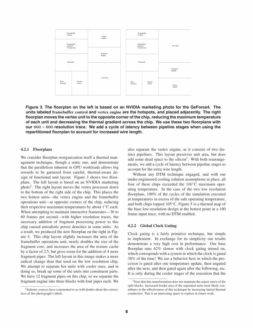
Figure 3. The floorplan on the left is based on an NVIDIA marketing photo for the GeForce4. Theunits labeled framebuffer control and vertex engine are the hotspots, and placed adjacently. The rightfloorplan moves the vertex unit to the opposite corner of the chip, reducing the maximum temperatureof each unit and decreasing the thermal gradient across the chip. We use these two floorplans withour 800 × 600 resolution trace. We add a cycle of latency between pipeline stages when using therepartitioned floorplan to account for increased wire length.
4.2.1 Floorplans
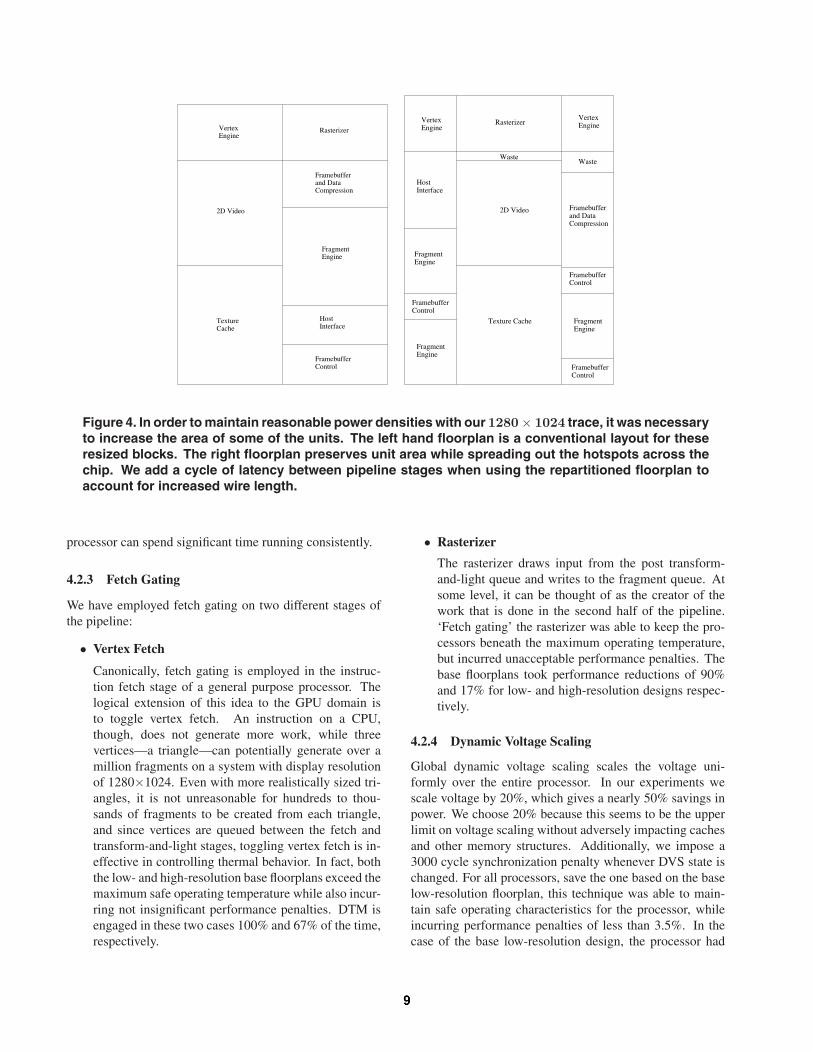
We consider floorplan reorganization itself a thermal man-agement technique, though a static one, and demonstratethat the parallelism inherent in GPU workloads allows bigrewards to be garnered from careful, thermal-aware de-sign of functional unit layout. Figure 3 shows two floor-plans. The left layout is based on an NVIDIA marketingphoto2. The right layout moves the vertex processor downto the bottom of the right side of the chip. This places thetwo hottest units—the vertex engine and the framebufferoperations unit—at opposite corners of the chip, reducingtheir respective maximum temperatures by about 1◦C each.When attempting to maintain interactive framerates—30 to60 frames per second—with higher resolution traces, thenecessary addition of fragment processing power to thischip caused unrealistic power densities in some units. Asa result, we produced the new floorplan on the right in Fig-ure 4. This chip layout slightly increases the area of theframebuffer operations unit, nearly doubles the size of thefragment core, and increases the area of the texture cacheby a factor of 2.5, but gives room for the addition of 4 morefragment pipes. The left layout in this image makes a moreradical change than that used on the low resolution chip.We attempt to separate hot units with cooler ones, and indoing so, break up some of the units into constituent parts.We have 12 fragment pipes on this chip, so we separate thefragment engine into three blocks with four pipes each. We
2Industry sources have commented to us with doubts about the correct-ness of this photograph’s labels.
also separate the vertex engine, as it consists of two dis-tinct pipelines. This layout preserves unit area, but doesadd some dead space to the silicon3. With both rearrange-ments, we add a cycle of latency between pipeline stages toaccount for the extra wire length.
Without any DTM technique engaged, and with ourunder-engineered cooling solution assumptions in place, allfour of these chips exceeded the 100◦C maximum oper-ating temperature. In the case of the two low resolutionfloorplans, 100% of the cycles of the simulation executedat temperatures in excess of the safe operating temperature,and both chips topped 105◦C. Figure 5 is a thermal map ofthe base low-resolution design at the hottest point in a 100frame input trace, with no DTM enabled.
4.2.2 Global Clock Gating
Clock gating is a fairly primitive technique, but simpleto implement. In exchange for its simplicity our resultsdemonstrate a very high cost in performance. Our basefloorplan runs 62% slower with clock gating turned on,which corresponds with a system in which the clock is gated38% of the time! We see a behavior here in which the pro-cessor is gated after one temperature update, then ungatedafter the next, and then gated again after the following, etc.It is only during the cooler stages of the execution that the
3Note that this transformation does not maintain the aspect ratios of thesplit blocks. Increased border area of the separated units most likely con-tributes to the effectiveness of this technique by increasing lateral thermalconduction. This is an interesting space to explore in future work.
VertexEngine
TextureCache
FramebufferControl
HostInterface
FragmentEngine
Framebufferand DataCompression
2D Video
Rasterizer
FramebufferControl
VertexEngine
FramebufferControl
FragmentEngine
FragmentEngine
HostInterface
VertexEngine
FramebufferControl
FragmentEngine
Framebufferand DataCompression
Waste
Rasterizer
Waste
2D Video
Texture Cache
Figure 4. In order to maintain reasonable power densities with our 1280 × 1024 trace, it was necessaryto increase the area of some of the units. The left hand floorplan is a conventional layout for theseresized blocks. The right floorplan preserves unit area while spreading out the hotspots across thechip. We add a cycle of latency between pipeline stages when using the repartitioned floorplan toaccount for increased wire length.
processor can spend significant time running consistently.
4.2.3 Fetch Gating
We have employed fetch gating on two different stages ofthe pipeline:
• Vertex Fetch
Canonically, fetch gating is employed in the instruc-tion fetch stage of a general purpose processor. Thelogical extension of this idea to the GPU domain isto toggle vertex fetch. An instruction on a CPU,though, does not generate more work, while threevertices—a triangle—can potentially generate over amillion fragments on a system with display resolutionof 1280×1024. Even with more realistically sized tri-angles, it is not unreasonable for hundreds to thou-sands of fragments to be created from each triangle,and since vertices are queued between the fetch andtransform-and-light stages, toggling vertex fetch is in-effective in controlling thermal behavior. In fact, boththe low- and high-resolution base floorplans exceed themaximum safe operating temperature while also incur-ring not insignificant performance penalties. DTM isengaged in these two cases 100% and 67% of the time,respectively.
• Rasterizer
The rasterizer draws input from the post transform-and-light queue and writes to the fragment queue. Atsome level, it can be thought of as the creator of thework that is done in the second half of the pipeline.‘Fetch gating’ the rasterizer was able to keep the pro-cessors beneath the maximum operating temperature,but incurred unacceptable performance penalties. Thebase floorplans took performance reductions of 90%and 17% for low- and high-resolution designs respec-tively.
4.2.4 Dynamic Voltage Scaling
Global dynamic voltage scaling scales the voltage uni-formly over the entire processor. In our experiments wescale voltage by 20%, which gives a nearly 50% savings inpower. We choose 20% because this seems to be the upperlimit on voltage scaling without adversely impacting cachesand other memory structures. Additionally, we impose a3000 cycle synchronization penalty whenever DVS state ischanged. For all processors, save the one based on the baselow-resolution floorplan, this technique was able to main-tain safe operating characteristics for the processor, whileincurring performance penalties of less than 3.5%. In thecase of the base low-resolution design, the processor had
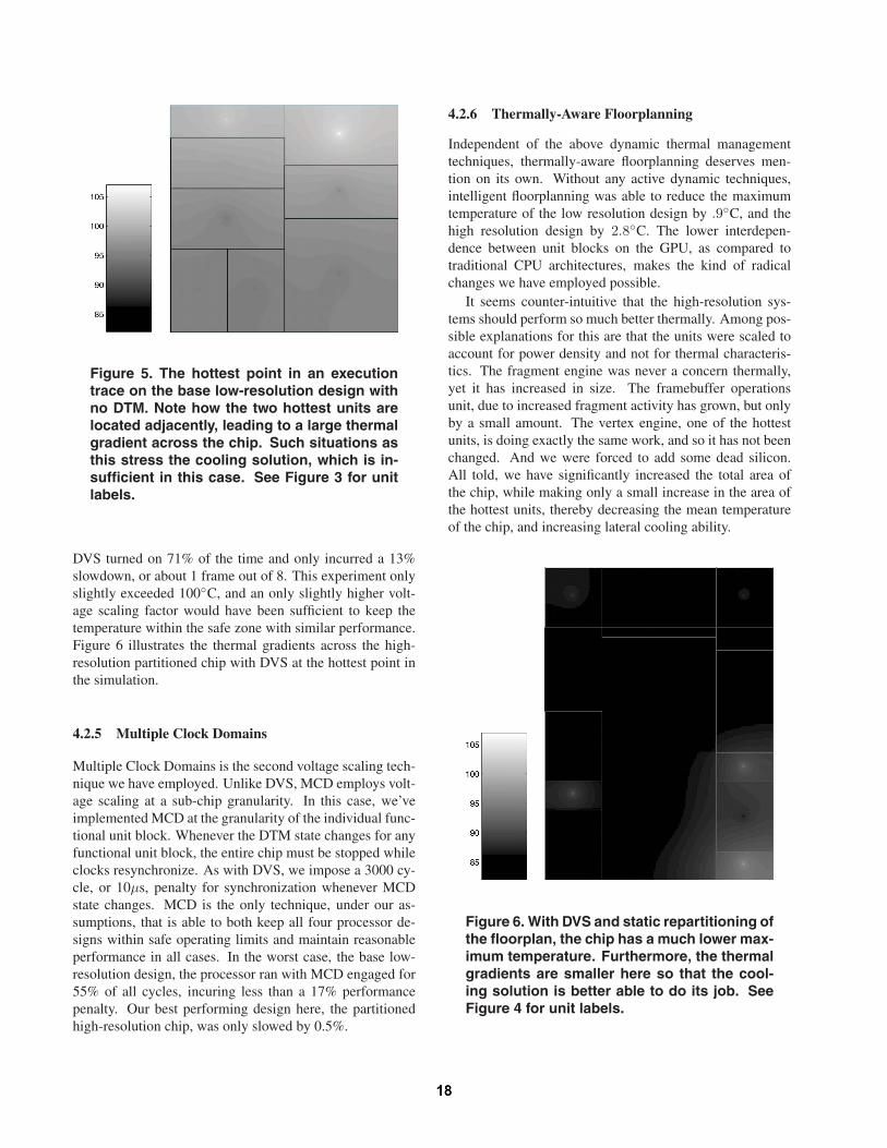
Figure 5. The hottest point in an executiontrace on the base low-resolution design withno DTM. Note how the two hottest units arelocated adjacently, leading to a large thermalgradient across the chip. Such situations asthis stress the cooling solution, which is in-sufficient in this case. See Figure 3 for unitlabels.
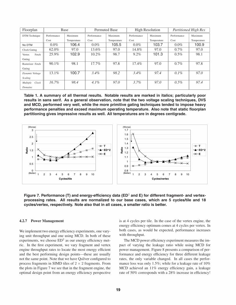
DVS turned on 71% of the time and only incurred a 13%slowdown, or about 1 frame out of 8. This experiment onlyslightly exceeded 100◦C, and an only slightly higher volt-age scaling factor would have been sufficient to keep thetemperature within the safe zone with similar performance.Figure 6 illustrates the thermal gradients across the high-resolution partitioned chip with DVS at the hottest point inthe simulation.
4.2.5 Multiple Clock Domains
Multiple Clock Domains is the second voltage scaling tech-nique we have employed. Unlike DVS, MCD employs volt-age scaling at a sub-chip granularity. In this case, we’veimplemented MCD at the granularity of the individual func-tional unit block. Whenever the DTM state changes for anyfunctional unit block, the entire chip must be stopped whileclocks resynchronize. As with DVS, we impose a 3000 cy-cle, or 10µs, penalty for synchronization whenever MCDstate changes. MCD is the only technique, under our as-sumptions, that is able to both keep all four processor de-signs within safe operating limits and maintain reasonableperformance in all cases. In the worst case, the base low-resolution design, the processor ran with MCD engaged for55% of all cycles, incuring less than a 17% performancepenalty. Our best performing design here, the partitionedhigh-resolution chip, was only slowed by 0.5%.
4.2.6 Thermally-Aware Floorplanning
Independent of the above dynamic thermal managementtechniques, thermally-aware floorplanning deserves men-tion on its own. Without any active dynamic techniques,intelligent floorplanning was able to reduce the maximumtemperature of the low resolution design by .9◦C, and thehigh resolution design by 2.8◦C. The lower interdepen-dence between unit blocks on the GPU, as compared totraditional CPU architectures, makes the kind of radicalchanges we have employed possible.
It seems counter-intuitive that the high-resolution sys-tems should perform so much better thermally. Among pos-sible explanations for this are that the units were scaled toaccount for power density and not for thermal characteris-tics. The fragment engine was never a concern thermally,yet it has increased in size. The framebuffer operationsunit, due to increased fragment activity has grown, but onlyby a small amount. The vertex engine, one of the hottestunits, is doing exactly the same work, and so it has not beenchanged. And we were forced to add some dead silicon.All told, we have significantly increased the total area ofthe chip, while making only a small increase in the area ofthe hottest units, thereby decreasing the mean temperatureof the chip, and increasing lateral cooling ability.
Figure 6. With DVS and static repartitioning ofthe floorplan, the chip has a much lower max-imum temperature. Furthermore, the thermalgradients are smaller here so that the cool-ing solution is better able to do its job. SeeFigure 4 for unit labels.
Floorplan Base Permuted Base High Resolution Partitioned High Res
DTM Technique Performance
Cost
Maximum
Temperature
Performance
Cost
Maximum
Temperature
Performance
Cost
Maximum
Temperature
Performance
Cost
Maximum
Temperature
No DTM 0.0% 106.4 0.0% 105.5 0.0% 103.7 0.0% 100.9Clock Gating 62.0% 97.0 13.6% 97.0 14.8% 97.0 0.7% 97.0Vertex Fetch
Gating
25.9% 102.9 10.2% 98.7 9.2% 101.3 0.5% 98.1
Rasterizer Fetch
Gating
90.1% 98.1 17.7% 97.8 17.4% 97.0 0.7% 97.8
Dynamic Voltage
Scaling
13.1% 100.7 3.4% 98.2 3.4% 97.4 0.1% 97.0
Multiple Clock
Domains
16.7% 98.4 4.1% 97.0 3.7% 97.0 0.5% 97.4
Table 1. A summary of all thermal results. Notable results are marked in italics; particularly poorresults in sans serif. As a general observation, note that the two voltage scaling techniques, DVSand MCD, performed very well, while the more primitive gating techniques tended to impose heavyperformance penalties and exceed maximum operating temperature. Also note that static floorplanpartitioning gives impressive results as well. All temperatures are in degrees centigrade.
0
0.5
1
1.5
2
2.5
3
1 2 3 4 5 6 7 8 9 10
Cycles/tile
Rat
io
T
ED^2
E
(Better)
(Worse)
0.8
0.9
1
1.1
1.2
1.3
1.4
1.5
1.6
1.7
1 2 3 4 5 6 7 8 9 10
Cycles/vertex
Rat
io
T
ED^2
E
(Better)
(Worse)
Figure 7. Performance (T) and energy-efficiency data (ED2 and E) for different fragment- and vertex-processing rates. All results are normalized to our base cases, which are 5 cycles/tile and 18cycles/vertex, respectively. Note also that in all cases, a smaller ratio is better.
4.2.7 Power Management
We implement two energy efficiency experiments, one vary-ing unit throughput and one using MCD. In both of theseexperiments, we choose ED2 as our energy efficiency met-ric. In the first experiment, we vary fragment and vertexengine throughput rates to locate the most energy efficientand the best performing design points—these are usuallynot the same point. Note that we have Qsilver configured toprocess fragments in SIMD tiles of 2 × 2 fragments. Fromthe plots in Figure 7 we see that in the fragment engine, theoptimal design point from an energy efficiency perspective
is at 4 cycles per tile. In the case of the vertex engine, theenergy efficiency optimum comes at 4 cycles per vertex. Inboth cases, as would be expected, performance increaseswith throughput.
The MCD power efficiency experiment measures the im-pact of varying the leakage ratio while using MCD forpower management. Figure 8 presents a comparison of per-formance and energy efficiency for three different leakagerates, the only variable changed. In all cases the perfor-mance loss was only 1.5%; while for a leakage rate of 10%MCD achieved an 11% energy efficiency gain, a leakagerate of 50% corresponds with a 28% increase in efficiency!
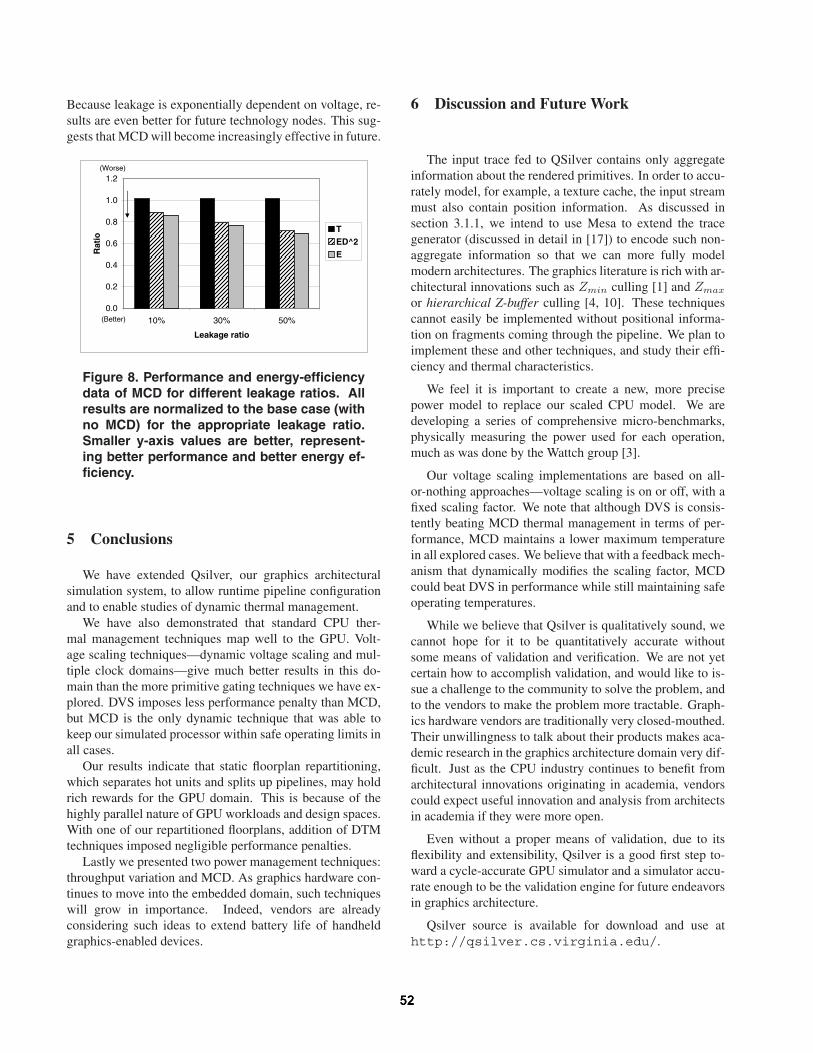
Because leakage is exponentially dependent on voltage, re-sults are even better for future technology nodes. This sug-gests that MCD will become increasingly effective in future.
0.0
0.2
0.4
0.6
0.8
1.0
1.2
10% 30% 50%
Leakage ratio
Rat
io
TED^2E
(Better)
(Worse)
Figure 8. Performance and energy-efficiencydata of MCD for different leakage ratios. Allresults are normalized to the base case (withno MCD) for the appropriate leakage ratio.Smaller y-axis values are better, represent-ing better performance and better energy ef-ficiency.
5 Conclusions
We have extended Qsilver, our graphics architecturalsimulation system, to allow runtime pipeline configurationand to enable studies of dynamic thermal management.
We have also demonstrated that standard CPU ther-mal management techniques map well to the GPU. Volt-age scaling techniques—dynamic voltage scaling and mul-tiple clock domains—give much better results in this do-main than the more primitive gating techniques we have ex-plored. DVS imposes less performance penalty than MCD,but MCD is the only dynamic technique that was able tokeep our simulated processor within safe operating limits inall cases.
Our results indicate that static floorplan repartitioning,which separates hot units and splits up pipelines, may holdrich rewards for the GPU domain. This is because of thehighly parallel nature of GPU workloads and design spaces.With one of our repartitioned floorplans, addition of DTMtechniques imposed negligible performance penalties.
Lastly we presented two power management techniques:throughput variation and MCD. As graphics hardware con-tinues to move into the embedded domain, such techniqueswill grow in importance. Indeed, vendors are alreadyconsidering such ideas to extend battery life of handheldgraphics-enabled devices.
6 Discussion and Future Work
The input trace fed to QSilver contains only aggregateinformation about the rendered primitives. In order to accu-rately model, for example, a texture cache, the input streammust also contain position information. As discussed insection 3.1.1, we intend to use Mesa to extend the tracegenerator (discussed in detail in [17]) to encode such non-aggregate information so that we can more fully modelmodern architectures. The graphics literature is rich with ar-chitectural innovations such as Zmin culling [1] and Zmax
or hierarchical Z-buffer culling [4, 10]. These techniquescannot easily be implemented without positional informa-tion on fragments coming through the pipeline. We plan toimplement these and other techniques, and study their effi-ciency and thermal characteristics.
We feel it is important to create a new, more precisepower model to replace our scaled CPU model. We aredeveloping a series of comprehensive micro-benchmarks,physically measuring the power used for each operation,much as was done by the Wattch group [3].
Our voltage scaling implementations are based on all-or-nothing approaches—voltage scaling is on or off, with afixed scaling factor. We note that although DVS is consis-tently beating MCD thermal management in terms of per-formance, MCD maintains a lower maximum temperaturein all explored cases. We believe that with a feedback mech-anism that dynamically modifies the scaling factor, MCDcould beat DVS in performance while still maintaining safeoperating temperatures.
While we believe that Qsilver is qualitatively sound, wecannot hope for it to be quantitatively accurate withoutsome means of validation and verification. We are not yetcertain how to accomplish validation, and would like to is-sue a challenge to the community to solve the problem, andto the vendors to make the problem more tractable. Graph-ics hardware vendors are traditionally very closed-mouthed.Their unwillingness to talk about their products makes aca-demic research in the graphics architecture domain very dif-ficult. Just as the CPU industry continues to benefit fromarchitectural innovations originating in academia, vendorscould expect useful innovation and analysis from architectsin academia if they were more open.
Even without a proper means of validation, due to itsflexibility and extensibility, Qsilver is a good first step to-ward a cycle-accurate GPU simulator and a simulator accu-rate enough to be the validation engine for future endeavorsin graphics architecture.
Qsilver source is available for download and use athttp://qsilver.cs.virginia.edu/.
7 Acknowledgments
This work is supported in part by the National Sci-ence Foundation under grant numbers CCR-0133634,CCR-0306404, Department of Energy grant numberDE-FG02-02ER25539, a grant from Intel MRL, and anExcellence Award from the University of Virginia Fund forExcellence in Science and Technology. The authors wouldalso like to thank the anonymous reviewers for their helpfulsuggestions.
References
[1] T. Akenine-Moller and J. Strom. Graphics for the masses: ahardware rasterization architecture for mobile phones. ACMTransactions on Graphics, 22(3):801–808, 2003.
[2] T. Austin, E. Larson, and D. Ernst. Simplescalar: An in-frastructure for computer system modeling. IEEE Computer,35(4):59–67, Feb. 2002.
[3] D. Brooks, V. Tiwari, and M. Martonosi. Wattch: A frame-work for architectural-level power analysis and optimiza-tions. In Proceedings of the 27th Annual International Sym-posium on Computer Architecture, pages 83–94, June 2000.
[4] N. Greene, M. Kass, and G. Miller. Hierarchical z-buffervisibility. In Proceedings of the 20th annual conference onComputer graphics and interactive techniques, pages 231–238. ACM Press, 1993.
[5] W. Huang, M. R. Stan, K. Skadron, S. Ghosh, K. Sankara-narayanan, and S. Velusamy. Compact thermal modeling fortemperature-aware design. In Proceedings of the 41st DesignAutomation Conference, June 2004.
[6] C. J. Hughes, V. S. Pai, P. Ranganathan, and S. V. Adve.Rsim: Simulating shared-memory multiprocessors with ilpprocessors. IEEE Computer, 35(4):40–49, Feb. 2002.
[7] G. Humphreys, M. Houston, R. Ng, S. Ahern, R. Frank,P. Kirchner, and J. T. Klosowski. Chromium: A streamprocessing framework for interactive graphics on clusters ofworkstations. ACM Transactions on Graphics, 21(3):693–702, July 2002.
[8] Y. Li, K. Skadron, Z. Hu, and D. Brooks. Understandingthe energy efficiency of simultaneous multithreading. In Pro-ceedings of the 2004 International Symposium on Low PowerElectronics and Design, Aug. 2004.
[9] P. S. Magnusson et al. Simics: A full system simulation plat-form. IEEE Computer, 35(4):50–58, Feb. 2002.
[10] S. Morein. ATI radeon HyperZ technology. Presentation atWorkshop on Graphics Hardware, Hot3D Proceedings, ACMSIGGRAPH/Eurographics, 2000.
[11] D. Nellans, V. K. Kadaru, and E. Brunvand. ASIM-An asyn-chronous architectural level simulator. In Proceedings ofGLSVLSI, April 2004.
[12] B. Paul et al. The mesa 3-d graphics library, 1993–2004.http://www.mesa3d.org/.
[13] K. Pulli. Graphics everywhere—pixels in yourpocket, 2004. Keynote Talk, Graphics Hardware2004, http://www.graphicshardware.org/Presentations/KariPulli.pdf.
[14] M. Rosenblum, S. A. Herrod, E. Witchel, and A. Gupta.Complete computer simulation: The SimOS approach. IEEEParallel and Distributed Technology: Systems and Applica-tions, 3(4):34–43, Winter 1995.
[15] D. Salvator. Preview: Nvidia’s geforce 6800 ultra,2004. http://www.extremetech.com/article2/0,1558,1566805,00.asp.
[16] G. Semeraro, G. Magklis, R. Balasubramonian, D. H. Al-bonesi, S. Dwarkadas, and M. L. Scott. Energy-efficient pro-cessor design using multiple clock domains with dynamicvoltage and frequency scaling. In Proceedings of the EighthInternational Symposium on High-Performance ComputerArchitecture, pages 29–40, Feb. 2002.
[17] J. W. Sheaffer, D. P. Luebke, and K. Skadron. A flexible sim-ulation framework for graphics architectures. In Proceedingsof Graphics Hardware 2004, Aug. 2004.
[18] J. W. Sheaffer, K. Skadron, and D. P. Luebke. Temperature-aware GPU design. Poster at ACM SIGGRAPH, Aug 2004.
[19] K. Skadron, K. Sankaranarayanan, S. Velusamy, D. Tarjan,M. R. Stan, and W. Huang. Temperature-aware microarchi-tecture: Modeling and implementation. ACM Transactionson Architecture and Code Optimization, 2004.
[20] K. Skadron, M. R. Stan, W. Huang, S. Velusamy, K. Sankara-narayanan, and D. Tarjan. Temperature-aware microarchitec-ture. In Proceedings of the 30th Annual International Sym-posium on Computer Architecture, pages 2–13, Apr. 2003.
[21] M. Vachharajani, N. Vachharajani, D. A. Penry, J. A. Blome,and D. I. August. Microarchitectural exploration with lib-erty. In Proceedings of the 35th International Symposium onMicroarchitecture, November 2002.