Embed Size (px)
Citation preview
Study of planar defect filtering in InP grown on
Si by epitaxial lateral overgrowth
Carl Junesand, Himanshu Kataria, Wondwosen Metaferia, Nick Julian, Zhechao Wang, Yan-
Ting Sun, John Bowers, Galia Pozina, Lars Hultman and Sebastian Lourdudoss
Linköping University Post Print
N.B.: When citing this work, cite the original article.
Original Publication:
Carl Junesand, Himanshu Kataria, Wondwosen Metaferia, Nick Julian, Zhechao Wang, Yan-
Ting Sun, John Bowers, Galia Pozina, Lars Hultman and Sebastian Lourdudoss, Study of
planar defect filtering in InP grown on Si by epitaxial lateral overgrowth, 2013, Optical
Materials Express, (3), 11, 1960-1973.
http://dx.doi.org/10.1364/OME.3.001960
Copyright: Optical Society of America
http://www.osa.org/
Postprint available at: Linköping University Electronic Press
http://urn.kb.se/resolve?urn=urn:nbn:se:liu:diva-102394
Study of planar defect filtering in InP grown on Si by epitaxial lateral overgrowth
Carl Junesand,1 Himanshu Kataria,1 Wondwosen Metaferia,1 Nick Julian,3 Zhechao Wang,1,2 Yan-Ting Sun,1 John Bowers,3 Galia Pozina,4 Lars Hultman,4 and Sebastian
Lourdudoss1,* 1 KTH-Royal Institute of Technology, Laboratory of Semiconductor Materials, Electrum 229, 16440 Kista, Sweden
2 Ghent University, Dept. of Information Technology, Sint-Pietersnieuwstraat 41, 9000 Ghent, Belgium 3 Department of Electrical and Computer Engineering, University of California, Santa Barbara, CA 93106, USA
4 Thin Film Physics Division, Department of Physics, Linköping University, 581 83 Linköping, Sweden *[email protected]
Abstract: InP thin films have been grown on InP/Si substrate by epitaxial lateral overgrowth (ELOG). The nature, origin and filtering of extended defects in ELOG layers grown from single and double openings in SiO2 mask have been investigated. Whereas ELOG layers grown from double openings occasionally exhibit threading dislocations (TDs) at certain points of coalescence, TDs are completely absent in ELOG from single openings. Furthermore, stacking faults (SFs) observed in ELOG layers grown from both opening types originate not from coalescence, but possibly from formation during early stages of ELOG or simply propagate from the seed layer through the mask openings. A model describing their propagation is devised and applied to the existent conditions, showing that SFs can effectively be filtered under certain conditions. ELOG layers grown from identical patterns on InP substrate contained no defects, indicating that the defect-forming mechanism is in any case not inherent to ELOG itself.
© 2013 Optical Society of America
OCIS codes: (130.3130) Integrated optics materials, (130.5990) Semiconductors, (160.4670) Optical materials, (310.1860) Deposition and fabrication, (250.1500) Cathodoluminescence.
References and links
1. B. Kunert, I. Németh, S. Reinhard, K. Volz, and W. Stolz, “Si (001) surface preparation for the antiphase domain free heteroepitaxial growth of GaP on Si substrate,” Thin Solid Films 517(1), 140–143 (2008).
2. R. Loo, G. Wang, T. Orzali, N. Waldron, C. Merckling, M. R. Leys, O. Richard, H. Bender, P. Eyben, W. Vandervorst, and M. Caymax, “Selective area growth of InP on On-Axis Si(001) substrates with low antiphase boundary formation,” J. Electrochem. Soc. 159(3), H260–H265 (2012).
3. Y. Nakamura, T. Miwa, and M. Ichikawa, “Nanocontact heteroepitaxy of thin GaSb and AlGaSb films on Si substrates using ultrahigh-density nanodot seeds,” Nanotechnology 22(26), 265301 (2011).
4. M. Sugiyama, Y. Kondo, M. Takenaka, S. Takagi, and Y. Nakano, “Uniformity improvement of selectively-grown InGaAs micro-discs on Si,” J. Cryst. Growth 352(1), 229–234 (2012).
5. K. Volz, A. Beyer, W. Witte, J. Ohlmann, I. Németh, B. Kunert, and W. Stolz, “GaP-nucleation on exact Si (001) substrates for III/V device integration,” J. Cryst. Growth 315(1), 37–47 (2011).
6. J. Bowers, D. Liang, A. Fang, H. Park, R. Jones, and M. Paniccia, “Hybrid silicon lasers,” Opt. Photonics News 21(5), 28–33 (2010).
7. M. Lamponi, S. Keyvaninia, C. Jany, F. Poingt, F. Lelarge, G. de Valicourt, G. Roelkens, D. Van Thourhout, S. Messaoudene, J.-M. Fedeli, and G. H. Duan, “Low-threshold heterogeneously integrated Inp/SOI lasers with a double adiabatic taper coupler,” IEEE Photon. Technol. Lett. 24(1), 76–78 (2012).
8. K. Tanabe, K. Watanabe, and Y. Arakawa, “III-V/Si hybrid photonic devices by direct fusion bonding,” Sci Rep 2, 349 (2012).
9. M. Sugo, H. Mori, Y. Sakai, and Y. Itoh, “Stable cw operation at room temperature of a 1.5-μm wavelength multiple quantum well laser on a Si substrate,” Appl. Phys. Lett. 60(4), 472 (1992).
10. S. Mahajan, “Defects in semiconductors and their effects,” Acta Mater. 48(1), 137–149 (2000). 11. A. Krost, M. Grundmann, D. Bimberg, and H. Cerva, “InP on patterned Si(001): defect reduction by application
of the necking mechanism,” J. Cryst. Growth 124(1-4), 207–212 (1992). 12. Y. S. Chang, S. Naritsuka, and T. Nishinaga, “Effect of growth temperature on epitaxial lateral overgrowth of
GaAs on Si substrate,” J. Cryst. Growth 174(1-4), 630–634 (1997).
#197451 - $15.00 USD Received 12 Sep 2013; revised 11 Oct 2013; accepted 13 Oct 2013; published 25 Oct 2013(C) 2013 OSA 1 November 2013 | Vol. 3, No. 11 | DOI:10.1364/OME.3.001960 | OPTICAL MATERIALS EXPRESS 1960
13. T. Paskova, D. Hommel, P. P. Paskov, V. Darakchieva, B. Monemar, M. Bockowski, T. Suski, I. Grzegory, F. Tuomisto, K. Saarinen, N. Ashkenov, and M. Schubert, “Effect of high-temperature annealing on the residual strain and bending of freestanding GaN films grown by hydride vapor phase epitaxy,” Appl. Phys. Lett. 88(14), 141909 (2006).
14. C. Junesand, C. Hu, Z. Wang, W. Metaferia, P. Dagur, G. Pozina, L. Hultman, and S. Lourdudoss, “Effect of the surface morphology of seed and mask layers on Inp grown on Si by epitaxial lateral overgrowth,” J. Electron. Mater. 41(9), 2345–2349 (2012).
15. D. K. Biegelsen, F. A. Ponce, A. J. Smith, and J. C. Tramontana, “Initial stages of epitaxial growth of GaAs on (100) silicon,” J. Appl. Phys. 61(5), 1856 (1987).
16. F. Ernst and P. Pirouz, “Formation of planar defects in the epitaxial growth of GaP on Si substrate by metal organic chemical-vapor deposition,” J. Appl. Phys. 64(9), 4526–4530 (1988).
17. Y. Chen, X. W. Lin, Z. Liliental-Weber, J. Washburn, J. F. Klem, and J. Y. Tsao, “Dislocation formation mechanism in strained InxGa1−xAs islands grown on GaAs(001) substrates,” Appl. Phys. Lett. 68(1), 111 (1996).
18. J. Zou, X. Z. Liao, D. J. H. Cockayne, and Z. M. Jiang, “Alternative mechanism for misfit dislocation generation during high-temperature Ge(Si)/Si (001) island growth,” Appl. Phys. Lett. 81(11), 1996–1998 (2002).
19. F. Olsson, M. Xie, S. Lourdudoss, I. Prieto, and P. Postigo, “Epitaxial lateral overgrowth of InP on Si from nano-openings: Theoretical and experimental indication for defect filtering throughout the grown layer,” J. Appl. Phys. 104(9), 093112 (2008).
20. A. S. Jordan, G. T. Brown, B. Cockayne, D. Brasen, and W. Bonner, “An analysis of dislocation reduction by impurity hardening in the liquid-encapsulated Czochralski growth of 111 InP,” J. Appl. Phys. 58(11), 4383 (1985).
21. I. Yonenaga and K. Sumino, “Dislocation velocity in indium phosphide,” Appl. Phys. Lett. 58(1), 48 (1991). 22. H. Suzuki, “Chemical interaction of solute atoms with dislocations,” Sci. Rep. Res. Inst. Tohoku Univ. [Med]
A4, 455–463 (1952). 23. D. B. Holt, “Transmission electron microscope observations on gap electroluminescent diode materials,” J.
Mater. Sci. 7(3), 265–278 (1972). 24. M. S. Abrahams, “Mechanism of thermal annihilation of stacking faults in Gaas,” J. Appl. Phys. 41(6), 2358
(1970). 25. C. Junesand, M.-H. Gau, Y.-T. Sun, S. Loududoss, I. Lo, J. Jimenez, P. A. Postigo, F. M. M. Sánchez, J.
Hernandez, S. Molina, A. Abdessamad, G. Pozina, L. Hultman, and P. Pirouz, “Defect reduction in heteroepitaxial InP on Si by epitaxial lateral overgrowth,” Manuscript, submitted to Materials Express (2013).
26. R. S. Barnes, “The climb of edge dislocations in face-centred cubic crystals,” Acta Metall. 2(3), 380–385 (1954). 27. A. Beyer, I. Németh, S. Liebich, J. Ohlmann, W. Stolz, and K. Volz, “Influence of crystal polarity on crystal
defects in GaP grown on exact Si (001),” J. Appl. Phys. 109(8), 083529 (2011). 28. Z. Wang, C. Junesand, W. Metaferia, C. Hu, L. Wosinski, and S. Lourdudoss, “III–Vs on Si for photonic
applications—A monolithic approach,” Mater. Sci. Eng. B 177(17), 1551–1557 (2012). 29. L. H. Kuo, L. Salamanca-Riba, B. J. Wu, G. M. Haugen, J. M. DePuydt, G. Hofler, and H. Cheng, “Generation
of degradation defects, stacking faults, and misfit dislocations in ZnSe-based films grown on GaAs,” J. Vac. Sci. Technol. B 13(4), 1694 (1995).
30. T. Walter and D. Gerthsen, “TEM analysis of epitaxial semiconductor layers with high stacking fault densities considering artifacts induced by the cross-section geometry,” Ultramicroscopy 81(3-4), 279–288 (2000).
31. K. Nozawa and Y. Horikoshi, “Effects of annealing on the structural properties of Gaas on Si(100) grown at a low temperature by migration-enhanced epitaxy,” Jpn. J. Appl. Phys. 29(Part 2, No. 4), L540–L543 (1990).
1. Introduction
Heteroepitaxy of lll-Vs such as GaAs and InP on Si has recently received renewed interest, not least in the quest for light sources integrated with Si [1–4]. Although some approaches, e.g. growth of almost lattice-matched GaP on Si, looks promising [5], heteroepitaxial InP-based devices on par with those achieved with bonding approaches have not been achieved [6–8]. Extended defects such as threading dislocations (TDs) and stacking faults (SFs) remain a challenge despite many attempts to counter them. The detrimental effect of these defects have been known for as long as optically active devices have been around, and decreasing their density is paramount to making heteroepitaxy a viable approach for monolithic integration of such devices with Si [9,10]. As avoiding defects during heteroepitaxy of severely mismatched materials is inherently difficult, several approaches focusing on mitigating not the defect formation at the heterointerface but the subsequent extension of such defects have been developed [2,9,11]. Of these approaches, epitaxial lateral overgrowth (ELOG), has been rather extensively explored and has produced encouraging results [3,4,12,13]. Even with this method, TDs may form during coalescence of merging growth
#197451 - $15.00 USD Received 12 Sep 2013; revised 11 Oct 2013; accepted 13 Oct 2013; published 25 Oct 2013(C) 2013 OSA 1 November 2013 | Vol. 3, No. 11 | DOI:10.1364/OME.3.001960 | OPTICAL MATERIALS EXPRESS 1961
fronts, but the same does not appear to be true for SFs [14]. Several theories aimed at explaining the formation of SFs in heteroepitaxy have been put forth [15–18], but as of yet, no study has been able to conclusively explain the presence of these defects in InP and other III-Vs on Si in ELOG layers.
In this investigation, defects in homoepitaxial as well as heteroepitaxial laterally overgrown InP layers are studied. Identical experiments are carried out on masked InP and InP (seed)/Si substrates, and both uncoalesced and coalesced ELOG layers are studied by Scanning Electron Microscopy (SEM), Panchromatic Cathodoluminescence (PCL) and Transmission Electron Microscopy (TEM). A model for explaining the propagation of SFs in the ELOG layers based on the observations is proposed.
2. Experimental
Four types of samples were considered: one type consisting of n-type InP (001) with 2° off-cut, designated type A, and the other three consisting of (001) Si off-cut 4° towards [111] with a ~2 µm thick InP seed layer deposited by metal organic vapor phase epitaxy (MOVPE), designated B, C and D. As mentioned earlier, the reason for considering both InP and InP/Si was to investigate formation of new defects, which could theoretically occur in both InP and InP/Si and propagation of existing defects, which naturally can only take place in the case of InP/Si since there are virtually no pre-existing defects in InP substrates. Since previous investigations indicate that polishing the rather rough InP seed layer has a beneficial effect on the subsequently grown ELOG layer [14], on samples of B, C and D, an additional ~5 µm thick InP layer was grown by HVPE directly on the InP/Si substrate to provide adequate margin for polishing. This regrown layer was then subjected to a two-step CMP process, the details of which can be found elsewhere [14], resulting in a final seed layer thickness of around 4 µm.
On samples of types A and B, 700 nm of SiO2 was deposited by plasma-enhanced chemical vapor deposition (PECVD) and patterned with two parallel line openings with varying opening separations of 300, 500 and 1000 nm according to the schematic drawing in Fig. 1(a). These samples had a fixed opening width of 300 nm. The line openings were placed at either 30° or 60° off [110]. On samples of types C and D, 400 nm SiO2 was deposited by PECVD and patterned with single line openings with varying opening widths of 250, and 400 nm, according to Fig. 1(b); these openings were always placed at 30° off [110]. The patterns were in all cases produced by electron-beam lithography (EBL) and reactive ion etching (RIE). To facilitate addressing the samples, hereafter we employ notations in the form of T-sX-wY-αZ, where T stand for the sample type, sX for the opening separation of X nm, wY for the opening width of Y nm, and αZ for the opening angle with respect to [110] of Z degrees. C and D lack “s” since they have only single openings (unlike A and B, which have double openings).
Fig. 1. Mask opening schematic of (a) double openings and (b) single openings. In the case of double openings, angle α was 30° and 60°, and separation s was 300, 500 and 1000 nm whereas in the case of single openings, width w was 250 and 400 nm, and the angle α was 30°.
#197451 - $15.00 USD Received 12 Sep 2013; revised 11 Oct 2013; accepted 13 Oct 2013; published 25 Oct 2013(C) 2013 OSA 1 November 2013 | Vol. 3, No. 11 | DOI:10.1364/OME.3.001960 | OPTICAL MATERIALS EXPRESS 1962
Thus, e.g., A-s500-w300-α60 denotes sample of type A containing openings of width 300 nm separated by 500 nm at an angle of 60° with respect to [110]. For all samples, InP ELOG was performed in a commercial low-pressure hydride vapor phase epitaxy reactor (LP-HVPE) at 20 mbar and 590 – 600 °C. V/III ratio was 8 – 10 by controlling the PH3 flow = 120 sccm and InCl flow = 12 – 15 sccm. On all samples except sample D, on which unintentionally doped InP (u. d. InP) was grown, sulfur-doped InP (InP:S) was grown by introducing a flow of H2S = 8 sccm resulting in a nominal sulfur concentration of 2x1018 cm−3. The total flow in the reactor with nitrogen as a carrier gas was 900 sccm in all cases.
The optical quality was characterized with room-temperature PCL in situ in a SEM using acceleration voltages ranging from 5 to 7 kV. A Peltier-cooled GaAs Photo Multiplier Tube (PMT) was used for data acquisition. Characterization of crystal defects was done in a TEM by cutting thin lamellae of samples at selected locations. In case where two beam-condition was used, several images were taken since the visibility of a defect with a particular Burgers vector depends on the diffraction vector. The TEM images shown in this paper however exhibited all defects present as verified by multiple images taken with different diffraction vectors.
3. Results and discussion
SEM images of InP:S ELOG layers grown from double openings on InP/Si on samples B-s500-w300-α30 and B-s300-w300-α60 are shown in Fig. 2(a) and Fig. 2(b), respectively; their corresponding PCL images are shown in Fig. 2(c) and Fig. 2(d), respectively. From the PCL image of B-s500-w300-α30 shown in Fig. 2(c), black spots can be seen lying along a line in the middle of the ELOG layer, thus indicating defects, most likely TDs created during coalescence between merging growth fronts. However the sample B-s300-w300-α60, imaged by PCL in Fig. 2(d), does not exhibit any black spots indicating that no TDs were formed during coalescence in this case.
Fig. 2. SEM image of InP:S ELOG on InP/Si of samples (a) B-s500-w300-α30 and (b) B-s300-w300-α60. (c) and (d): PCL maps corresponding to the SEM images in (a) and (b), respectively.
Cross-sectional TEM images of ELOG InP:S on InP/Si of samples B-s500-w300-α30 and B-s1000-w300-α30, presented in Fig. 3, and similar images of samples B-s300-w300-α60 and B-s500-w300-α60, presented in Fig. 4, provide additional information that partly confirms the
#197451 - $15.00 USD Received 12 Sep 2013; revised 11 Oct 2013; accepted 13 Oct 2013; published 25 Oct 2013(C) 2013 OSA 1 November 2013 | Vol. 3, No. 11 | DOI:10.1364/OME.3.001960 | OPTICAL MATERIALS EXPRESS 1963
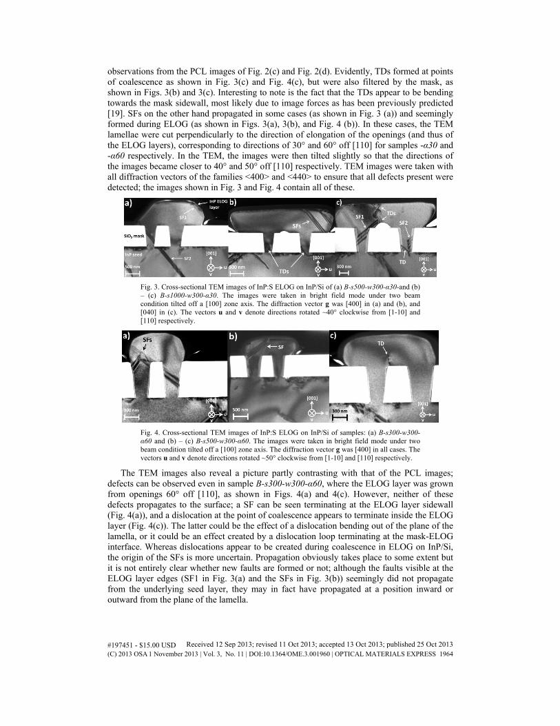
observations from the PCL images of Fig. 2(c) and Fig. 2(d). Evidently, TDs formed at points of coalescence as shown in Fig. 3(c) and Fig. 4(c), but were also filtered by the mask, as shown in Figs. 3(b) and 3(c). Interesting to note is the fact that the TDs appear to be bending towards the mask sidewall, most likely due to image forces as has been previously predicted [19]. SFs on the other hand propagated in some cases (as shown in Fig. 3 (a)) and seemingly formed during ELOG (as shown in Figs. 3(a), 3(b), and Fig. 4 (b)). In these cases, the TEM lamellae were cut perpendicularly to the direction of elongation of the openings (and thus of the ELOG layers), corresponding to directions of 30° and 60° off [110] for samples -α30 and -α60 respectively. In the TEM, the images were then tilted slightly so that the directions of the images became closer to 40° and 50° off [110] respectively. TEM images were taken with all diffraction vectors of the families <400> and <440> to ensure that all defects present were detected; the images shown in Fig. 3 and Fig. 4 contain all of these.
Fig. 3. Cross-sectional TEM images of InP:S ELOG on InP/Si of (a) B-s500-w300-α30-and (b) – (c) B-s1000-w300-α30. The images were taken in bright field mode under two beam condition tilted off a [100] zone axis. The diffraction vector g was [400] in (a) and (b), and [040] in (c). The vectors u and v denote directions rotated ~40° clockwise from [1-10] and [110] respectively.
Fig. 4. Cross-sectional TEM images of InP:S ELOG on InP/Si of samples: (a) B-s300-w300-α60 and (b) – (c) B-s500-w300-α60. The images were taken in bright field mode under two beam condition tilted off a [100] zone axis. The diffraction vector g was [400] in all cases. The vectors u and v denote directions rotated ~50° clockwise from [1-10] and [110] respectively.
The TEM images also reveal a picture partly contrasting with that of the PCL images; defects can be observed even in sample B-s300-w300-α60, where the ELOG layer was grown from openings 60° off [110], as shown in Figs. 4(a) and 4(c). However, neither of these defects propagates to the surface; a SF can be seen terminating at the ELOG layer sidewall (Fig. 4(a)), and a dislocation at the point of coalescence appears to terminate inside the ELOG layer (Fig. 4(c)). The latter could be the effect of a dislocation bending out of the plane of the lamella, or it could be an effect created by a dislocation loop terminating at the mask-ELOG interface. Whereas dislocations appear to be created during coalescence in ELOG on InP/Si, the origin of the SFs is more uncertain. Propagation obviously takes place to some extent but it is not entirely clear whether new faults are formed or not; although the faults visible at the ELOG layer edges (SF1 in Fig. 3(a) and the SFs in Fig. 3(b)) seemingly did not propagate from the underlying seed layer, they may in fact have propagated at a position inward or outward from the plane of the lamella.
#197451 - $15.00 USD Received 12 Sep 2013; revised 11 Oct 2013; accepted 13 Oct 2013; published 25 Oct 2013(C) 2013 OSA 1 November 2013 | Vol. 3, No. 11 | DOI:10.1364/OME.3.001960 | OPTICAL MATERIALS EXPRESS 1964
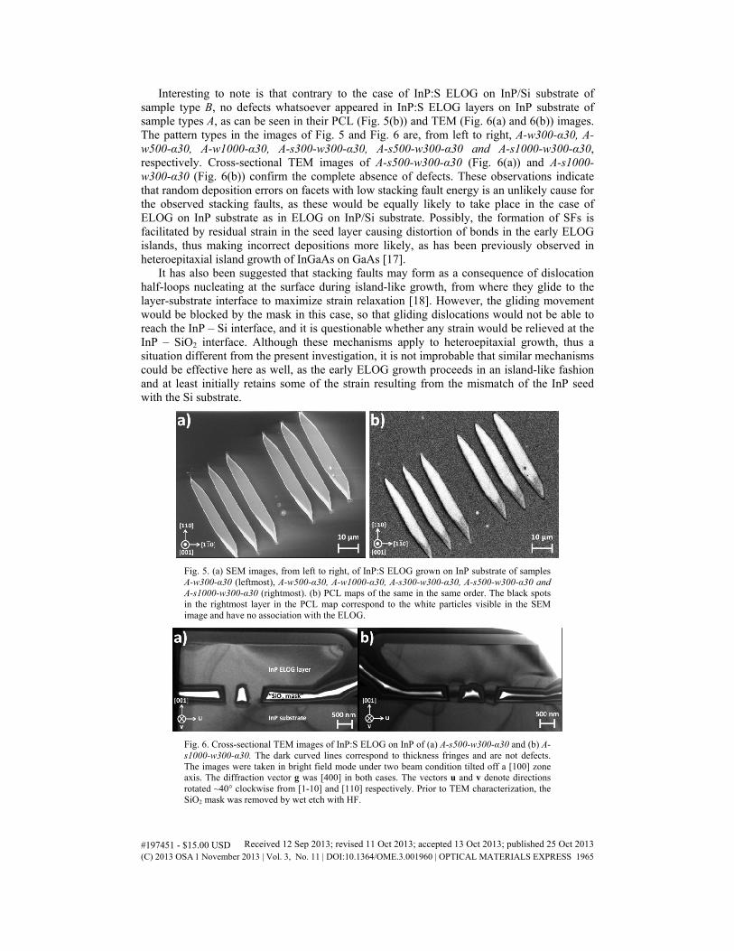
Interesting to note is that contrary to the case of InP:S ELOG on InP/Si substrate of sample type B, no defects whatsoever appeared in InP:S ELOG layers on InP substrate of sample types A, as can be seen in their PCL (Fig. 5(b)) and TEM (Fig. 6(a) and 6(b)) images. The pattern types in the images of Fig. 5 and Fig. 6 are, from left to right, A-w300-α30, A-w500-α30, A-w1000-α30, A-s300-w300-α30, A-s500-w300-α30 and A-s1000-w300-α30, respectively. Cross-sectional TEM images of A-s500-w300-α30 (Fig. 6(a)) and A-s1000-w300-α30 (Fig. 6(b)) confirm the complete absence of defects. These observations indicate that random deposition errors on facets with low stacking fault energy is an unlikely cause for the observed stacking faults, as these would be equally likely to take place in the case of ELOG on InP substrate as in ELOG on InP/Si substrate. Possibly, the formation of SFs is facilitated by residual strain in the seed layer causing distortion of bonds in the early ELOG islands, thus making incorrect depositions more likely, as has been previously observed in heteroepitaxial island growth of InGaAs on GaAs [17].
It has also been suggested that stacking faults may form as a consequence of dislocation half-loops nucleating at the surface during island-like growth, from where they glide to the layer-substrate interface to maximize strain relaxation [18]. However, the gliding movement would be blocked by the mask in this case, so that gliding dislocations would not be able to reach the InP – Si interface, and it is questionable whether any strain would be relieved at the InP – SiO2 interface. Although these mechanisms apply to heteroepitaxial growth, thus a situation different from the present investigation, it is not improbable that similar mechanisms could be effective here as well, as the early ELOG growth proceeds in an island-like fashion and at least initially retains some of the strain resulting from the mismatch of the InP seed with the Si substrate.
Fig. 5. (a) SEM images, from left to right, of InP:S ELOG grown on InP substrate of samples A-w300-α30 (leftmost), A-w500-α30, A-w1000-α30, A-s300-w300-α30, A-s500-w300-α30 and A-s1000-w300-α30 (rightmost). (b) PCL maps of the same in the same order. The black spots in the rightmost layer in the PCL map correspond to the white particles visible in the SEM image and have no association with the ELOG.
Fig. 6. Cross-sectional TEM images of InP:S ELOG on InP of (a) A-s500-w300-α30 and (b) A-s1000-w300-α30. The dark curved lines correspond to thickness fringes and are not defects. The images were taken in bright field mode under two beam condition tilted off a [100] zone axis. The diffraction vector g was [400] in both cases. The vectors u and v denote directions rotated ~40° clockwise from [1-10] and [110] respectively. Prior to TEM characterization, the SiO2 mask was removed by wet etch with HF.
#197451 - $15.00 USD Received 12 Sep 2013; revised 11 Oct 2013; accepted 13 Oct 2013; published 25 Oct 2013(C) 2013 OSA 1 November 2013 | Vol. 3, No. 11 | DOI:10.1364/OME.3.001960 | OPTICAL MATERIALS EXPRESS 1965
The fact that the ELOG layers grown on InP/Si are less uniform in shape compared to those grown on InP could be an indication of strain-relaxation as the ELOG layer is free to adjust to its natural lattice constant outside the opening, or, as mentioned previously, due to strain-distorted bonds causing growth to take place more irregularly. Possibly, it could be an effect of the substrate off-cut angle. However, the InP substrate was also off-cut though to a lower degree (2°), and in another study where InP/Si substrates with a larger off-cut angle (6°) were used, no signs of similar deformation could be seen, though macro steps could be observed [2]. Thus, a more thorough thermal annealing of the InP seed layer on Si prior to ELOG may release enough of this residual stress to prevent faulting during subsequent ELOG. Also, annealing after early ELOG prior to coalescence, when any residual strain should have been relaxed by un-distorting elastically, should remove any faults formed during ELOG since their removal would lower the total energy in the crystal.
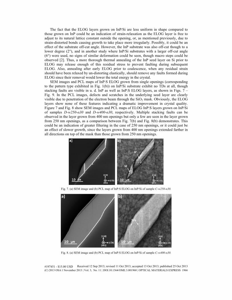
SEM images and PCL maps of InP:S ELOG grown from single openings (corresponding to the pattern type exhibited in Fig. 1(b)) on InP/Si substrate exhibit no TDs at all, though stacking faults are visible in u. d. InP as well as InP:S ELOG layers, as shown in Figs. 7 – Fig. 9. In the PCL images, defects and scratches in the underlying seed layer are clearly visible due to penetration of the electron beam through the SiO2 mask. Obviously, the ELOG layers show none of these features indicating a dramatic improvement in crystal quality. Figure 7 and Fig. 8 show SEM images and PCL maps of ELOG InP:S layers grown on InP/Si of samples D-w250-α30 and D-w400-α30, respectively. Multiple stacking faults can be observed in the layer grown from 400 nm openings but only a few are seen in the layer grown from 250 nm openings, as a comparison between Fig. 7(b) and Fig. 8(b) demonstrates. This could be an indication of greater filtering in the case of 250 nm openings, or it could just be an effect of slower growth, since the layers grown from 400 nm openings extended farther in all directions on top of the mask than those grown from 250 nm openings.
Fig. 7. (a) SEM image and (b) PCL map of InP:S ELOG on InP/Si of sample C-w250-α30.
Fig. 8. (a) SEM image and (b) PCL map of InP:S ELOG on InP/Si of sample C-w400-α30.
#197451 - $15.00 USD Received 12 Sep 2013; revised 11 Oct 2013; accepted 13 Oct 2013; published 25 Oct 2013(C) 2013 OSA 1 November 2013 | Vol. 3, No. 11 | DOI:10.1364/OME.3.001960 | OPTICAL MATERIALS EXPRESS 1966
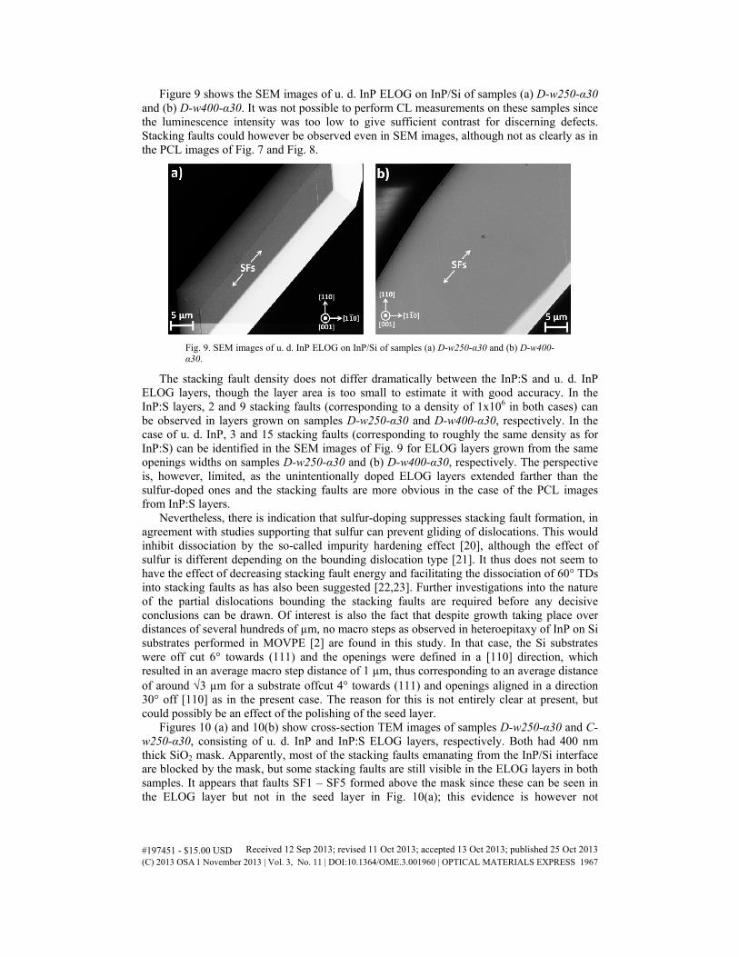
Figure 9 shows the SEM images of u. d. InP ELOG on InP/Si of samples (a) D-w250-α30 and (b) D-w400-α30. It was not possible to perform CL measurements on these samples since the luminescence intensity was too low to give sufficient contrast for discerning defects. Stacking faults could however be observed even in SEM images, although not as clearly as in the PCL images of Fig. 7 and Fig. 8.
Fig. 9. SEM images of u. d. InP ELOG on InP/Si of samples (a) D-w250-α30 and (b) D-w400-α30.
The stacking fault density does not differ dramatically between the InP:S and u. d. InP ELOG layers, though the layer area is too small to estimate it with good accuracy. In the InP:S layers, 2 and 9 stacking faults (corresponding to a density of 1x10⁶ in both cases) can be observed in layers grown on samples D-w250-α30 and D-w400-α30, respectively. In the case of u. d. InP, 3 and 15 stacking faults (corresponding to roughly the same density as for InP:S) can be identified in the SEM images of Fig. 9 for ELOG layers grown from the same openings widths on samples D-w250-α30 and (b) D-w400-α30, respectively. The perspective is, however, limited, as the unintentionally doped ELOG layers extended farther than the sulfur-doped ones and the stacking faults are more obvious in the case of the PCL images from InP:S layers.
Nevertheless, there is indication that sulfur-doping suppresses stacking fault formation, in agreement with studies supporting that sulfur can prevent gliding of dislocations. This would inhibit dissociation by the so-called impurity hardening effect [20], although the effect of sulfur is different depending on the bounding dislocation type [21]. It thus does not seem to have the effect of decreasing stacking fault energy and facilitating the dissociation of 60° TDs into stacking faults as has also been suggested [22,23]. Further investigations into the nature of the partial dislocations bounding the stacking faults are required before any decisive conclusions can be drawn. Of interest is also the fact that despite growth taking place over distances of several hundreds of µm, no macro steps as observed in heteroepitaxy of InP on Si substrates performed in MOVPE [2] are found in this study. In that case, the Si substrates were off cut 6° towards (111) and the openings were defined in a [110] direction, which resulted in an average macro step distance of 1 µm, thus corresponding to an average distance of around √3 µm for a substrate offcut 4° towards (111) and openings aligned in a direction 30° off [110] as in the present case. The reason for this is not entirely clear at present, but could possibly be an effect of the polishing of the seed layer.
Figures 10 (a) and 10(b) show cross-section TEM images of samples D-w250-α30 and C-w250-α30, consisting of u. d. InP and InP:S ELOG layers, respectively. Both had 400 nm thick SiO2 mask. Apparently, most of the stacking faults emanating from the InP/Si interface are blocked by the mask, but some stacking faults are still visible in the ELOG layers in both samples. It appears that faults SF1 – SF5 formed above the mask since these can be seen in the ELOG layer but not in the seed layer in Fig. 10(a); this evidence is however not
#197451 - $15.00 USD Received 12 Sep 2013; revised 11 Oct 2013; accepted 13 Oct 2013; published 25 Oct 2013(C) 2013 OSA 1 November 2013 | Vol. 3, No. 11 | DOI:10.1364/OME.3.001960 | OPTICAL MATERIALS EXPRESS 1967
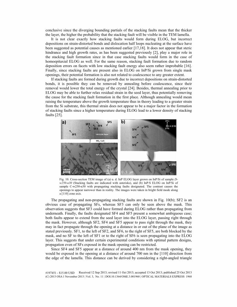
conclusive since the diverging bounding partials of the stacking faults mean that the thicker the layer, the higher the probability that the stacking fault will be visible in the TEM lamella.
It is not clear exactly how stacking faults would form during ELOG, but incorrect depositions on strain-distorted bonds and dislocation half loops nucleating at the surface have been suggested as potential causes as mentioned earlier [17,18]. It does not appear that steric hindrance and high growth rates, as has been suggested previously [2], play a major role in the stacking fault formation since in that case stacking faults would form in the case of homoepitaxial ELOG as well. For the same reason, stacking fault formation due to random deposition errors on facets with low stacking fault energy also seem rather improbable [16]. Finally, since stacking faults are present also in ELOG on InP/Si grown from single mask openings, their potential formation is also not related to coalescence to any greater extent.
If stacking faults are formed during growth due to incorrect depositions on strain-distorted bonds, it is possible they can be removed by annealing before coalescence, since their removal would lower the total energy of the crystal [24]. Besides, thermal annealing prior to ELOG may be able to further relax residual strain in the seed layer, thus potentially removing the cause for the stacking fault formation in the first place. Although annealing would mean raising the temperature above the growth temperature thus in theory leading to a greater strain from the Si substrate, this thermal strain does not appear to be a major factor in the formation of stacking faults since a higher temperature during ELOG lead to a lower density of stacking faults [25].
Fig. 10. Cross-section TEM image of (a) u. d. InP ELOG layer grown on InP/Si of sample D-w250-α30 (Stacking faults are indicated with asterisks), and (b) InP:S ELOG on InP/Si of sample C-w250-α30 with propagating stacking faults designated. The contrast causes the openings to appear narrower than in reality. The images were taken in bright field mode along a [110] zone axis.
The propagating and non-propagating stacking faults are shown in Fig. 10(b); SF2 is an obvious case of propagating SFs, whereas SF3 can only be seen above the mask. This observation suggests that SF3 could have formed during ELOG rather than propagating from underneath. Finally, the faults designated SF4 and SF5 present a somewhat ambiguous case; both faults appear to extend from the seed layer into the ELOG layer, passing right through the mask. However, although SF2, SF4 and SF5 appear to pass right through the mask, they may in fact propagate through the opening at a distance in or out of the plane of the image as stated previously. SF1, to the left of SF2, and SF6, to the right of SF5, are both blocked by the mask, and no SF to the left of SF1 or to the right of SF6 is seen propagating into the ELOG layer. This suggests that under certain experimental conditions with optimal pattern designs, propagation even of SFs exposed in the mask opening can be restricted.
Since SF4 and SF5 appear at a distance of around 400 nm from the mask opening, they would be exposed in the opening at a distance of around 700 nm in the [110] direction from the edge of the lamella. This distance can be derived by considering a right-angled triangle
#197451 - $15.00 USD Received 12 Sep 2013; revised 11 Oct 2013; accepted 13 Oct 2013; published 25 Oct 2013(C) 2013 OSA 1 November 2013 | Vol. 3, No. 11 | DOI:10.1364/OME.3.001960 | OPTICAL MATERIALS EXPRESS 1968
between the [110] direction, the [1-10] direction and the opening. With the distance 400 nm constituting the base of the triangle and the angle between the [110] direction and the opening being 30°, the height of the triangle corresponding to the distance in the [110] direction becomes 400/tan(30°) = 692.8… ~700 nm. Since most of the stacking faults are extending from the interface between the Si substrate and the roughly 4 µm thick seed layer, they would thus have a width of around the same size at the seed layer surface since the increase in stacking fault width has previously been found to scale with layer thickness with a relation of roughly 1:1 [25]. Consequently, it is probable that SF4 and SF5 are indeed exposed in the opening at some point. As mentioned, SF1 and SF6 are not seen propagating into the ELOG layer. This is especially interesting since SF4 and SF5 appear at a distance of around 400 nm from the mask opening, whereas SF1 appears only 270 nm away from the opening. Thus, if SF4 and SF5 were exposed in the mask opening at a distance in the [110] or [-1-10] direction from the lamella, then so should SF1 be at some point, assuming its extension in the [110] direction was roughly the same as that of SF4 and SF5.
However, since all faults SF1 – SF6 are facing the left sidewall, part of the latter fault may have terminated at this sidewall in the exposed region. The probability that SF4 or SF5 would terminate at the left sidewall is obviously lower since they are seen intersecting the seed – layer-mask interface to the right of the opening rather than to the left. As mentioned, the stacking faults to the left of SF2 and to the right of SF5 do not appear to be propagating into the ELOG layer, suggesting that they were blocked entirely at the seed layer – mask interface.
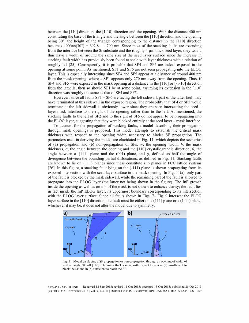
To account for the propagation of stacking faults, a model describing their propagation through mask openings is proposed. This model attempts to establish the critical mask thickness with respect to the opening width necessary to hinder SF propagation. The parameters used in deriving the model are elucidated in Fig. 11, which depicts the scenarios of (a) propagation and (b) non-propagation of SFs: w, the opening width, h, the mask thickness, α, the angle between the opening and the [110] crystallographic direction, θ, the angle between a {111} plane and the (001) plane, and φ, defined as half the angle of divergence between the bounding partial dislocations, as defined in Fig. 11. Stacking faults are known to lie on {111} planes since these constitute slip planes in FCC lattice systems [26]. In this figure, a stacking fault lying on the (-111) plane is shown propagating from its exposed intersection with the seed layer surface in the mask opening. In Fig. 11(a), only part of the fault is blocked by the mask sidewall, while the remaining part of the fault is allowed to propagate into the ELOG layer (the latter not being shown in the figure). The InP growth inside the opening as well as on top of the mask is not shown to enhance clarity; the fault lies in fact inside the InP ELOG layer, its uppermost boundary corresponding to its intersection with the ELOG layer surface. Since all faults shown in Figs. 7– Fig. 9 intersect the ELOG layer surface in the [110] direction, the fault must lie either on a (111) plane or a (1-11) plane; whichever it may be, it does not alter the model due to symmetry.
Fig. 11. Model displaying a SF propagation or non-propagation through an opening of width of w at an angle 30° off [110]. The mask thickness, h, with respect to w is in (a) insufficient to block the SF and in (b) sufficient to block the SF.
#197451 - $15.00 USD Received 12 Sep 2013; revised 11 Oct 2013; accepted 13 Oct 2013; published 25 Oct 2013(C) 2013 OSA 1 November 2013 | Vol. 3, No. 11 | DOI:10.1364/OME.3.001960 | OPTICAL MATERIALS EXPRESS 1969
By studying Fig. 11, it is apparent that it is the direction of one of the bounding partial dislocations which imposes the boundary condition for whether the propagation will take place or not; more specifically, it is the direction of the partial dislocation inclined towards a direction facing away from the blocking sidewall which is of critical importance (denoted by r in Fig. 11(b)). This is taken into account in the dependency on the angle φ, which, in case of a symmetrical SF, is half the angle between the two bounding partial dislocations, i.e. the angle with which they diverge from each other.
In Fig. 11, the stacking fault intersection with the seed layer surface extends across the entire opening. This situation corresponds to the greatest mask thickness for which propagation is still possible, since the closer the bounding partial r is to the right-hand sidewall, the lower the thickness at which the stacking fault will be blocked. If the stacking fault originated at the left-hand sidewall, there is also a possibility that the opposite partial (and thus the entire fault) would propagate as well, but the intersection with the sidewall (and thus blocking) of this partial would still take place at a lower height, so that the boundary condition for propagation would still be defined by r.
With the angles defined in Fig. 11, the length r of the bounding partial r becomes:
sin cos
hr
θ ϕ=
⋅ (1)
where h is the mask thickness. The length of the projection r’ of r on the (001) plane becomes:
tan
sin 90 arc tancos
wr
ϕαϕ
′ = ° − −
(2)
where w is the opening width. Finally, the relation between h, r and r’ is described by:
2 2 2r r h′= + (3) By combining Eqs. (1), (2), and (3), the expression for the mask height at which the
stacking fault is completely blocked becomes:
( ) ( )( )
2
2
1
tan 1sin 90 arc tan 1
cos sin cos
h wϕαθ θ ϕ
°
= − − ⋅ −
(4)
It should be noted that the model is valid only for certain combinations of angles of α and φ; more specifically, the angle in the sine expression in Eq. (2) must be greater than zero:
tan
90 arc tan 0cos
ϕβ αθ
° = − − > °
(5)
This condition basically states that the bounding partials must terminate at the mask sidewall in the direction of propagation of the stacking fault in order for blocking to be possible; if the angle of bounding partial divergence or the opening direction angle α is sufficiently large, blocking will not be possible. For example, in case of an angle φ = 30°, an opening angle α of 45° or greater would always allow the fault to propagate since part of the stacking fault would be exposed in the opening even at the top of the mask regardless of its height. It follows that if the SFs would intersect the layer surface along the [1-10] direction instead, then for the same φ, the opening angle α would have to be greater than 45° (and smaller than 135°) to allow filtering. It would thus not be possible to filter faults of both types simultaneously. However, SFs intersecting the layer in the [1-10] were not observed in this
#197451 - $15.00 USD Received 12 Sep 2013; revised 11 Oct 2013; accepted 13 Oct 2013; published 25 Oct 2013(C) 2013 OSA 1 November 2013 | Vol. 3, No. 11 | DOI:10.1364/OME.3.001960 | OPTICAL MATERIALS EXPRESS 1970
investigation, and a similar SF polarity has been observed in other heteroepitaxial systems such as GaP on Si [27].
The angle α is given by the angle between the opening direction and the [110] crystallographic direction, θ is the angle which the stacking fault makes with the (001) plane and φ is the angle with which the bounding partials diverge from [1-12], the direction in which the stacking fault propagates. The angle α is determined simply by observing the intersection lines of stacking faults with the ELOG surface (which can be either [110] or [1-10]) and the angle they make with the opening direction, which in this case becomes 30° since the faults’ intersection lines with the ELOG layer surfaces lie exclusively along [110] and the opening angle with respect to [110] is an experimental parameter set to be 30° since this angle is beneficial to the lateral growth rate. Thus, even though a smaller angle α would lead to a lower mask thickness necessary to achieve filtering, it would also lead to a smaller lateral growth rate which is of greater concern than the mask thickness. The reason for this is that whereas a thicker SiO2 has no particular detrimental effect, a thicker ELOG layer would mean lower coupling efficiency between an active device and a potential waveguide [28]. The angle θ is extracted from cross-section TEM images or simply by acknowledging that stacking faults lie on {111} planes in ZB crystals which make an angle to the (001) plane of roughly 55°.
The angle φ is somewhat more difficult to determine without knowing the nature of the stacking fault; it may in fact not even be constant but can vary as the bounding partials may continuously change direction. In the model however, φ and r can be thought of as representing the average diverging angle and direction respectively. It is however not unreasonable to assume that the partial dislocations bounding the stacking fault propagate along <011> and <101>, since these are natural bounding vectors for {111} planes as they together with <110> represent the directions of the shortest interatomic distance on {111} planes. Indeed, this is also what has been observed experimentally [29,30], though stacking faults bounded by partials in the <112> directions in GaAs on Si has also been observed [31]. Also, in a recent study, SF width increased with layer thickness in a way suggesting a 60° angle at most between the bounding partials, suggesting that the bounding partials lie in the <101> and <011> directions [25].
It is easily realized by looking at Fig. 11 that the smaller the angle φ, the smaller the height at which the stacking fault would be blocked for a given opening width. Thus, bounding partials in the <101> and <011> directions constitute a stricter requirement on the height than those in the <112> directions. Although the propagating stacking faults likely have a width at the intersection with the seed layer surface greater than the opening width, it is in this case assumed that the exposed part of the stacking faults will grow in the same way as an unobstructed fault would. Since bounding partials in the <101> and <011> directions correspond to an angle of divergence of 60°, they correspond to an angle φ of 30°. How exactly the exposed part of the SF would behave is however far from trivial to predict and likely depends on factors such as how the growth takes place inside the opening as well as interaction with strain fields from the SiO2 mask.
Using the angles for {111} planes and openings angled 30° off [110], α = 30°, θ ≈55° and φ = 30° in (4), h ≈3.9w. If, on the other hand, the bounding partials extend along <112> directions, thus corresponding to an angle φ = 0°, h decreases to ≈1.6w. Consequently, given the assumptions stated above, the ratio of mask height to opening width should be greater than 3.9 to ensure complete blocking of stacking faults. With a mask thickness of 400 nm, as in the case of ELOG layers grown on samples C-w250-α30 and D-w250-α30 (both with an opening width of 250 nm), this ratio becomes only 1.6, so that the fact that stacking faults are seen propagating through the openings, see Fig. 10(b), is in agreement with the model and the current assumptions. With the same mask thickness and openings width of 400 nm, the ratio decreases further to 1, thus increasing the probability of propagating stacking faults. Even in the case of samples of type B, with mask thickness of 700 nm and opening width 300 nm,
#197451 - $15.00 USD Received 12 Sep 2013; revised 11 Oct 2013; accepted 13 Oct 2013; published 25 Oct 2013(C) 2013 OSA 1 November 2013 | Vol. 3, No. 11 | DOI:10.1364/OME.3.001960 | OPTICAL MATERIALS EXPRESS 1971
propagation is possible according to the model with the current assumptions since the h to w ratio becomes 2.3 in that case, see e.g. Figure 3(a).
Since no samples with h to w ratios of 3.9 and greater were available, the applicability of the model and the accuracy of the assumptions cannot be decisively verified. However, evidence of stacking faults terminating at a mask sidewall would lend some support to the suggested hypothesis since this would mean that the propagation of stacking faults at least may be hindered by mask sidewalls. This actually is the case is seen in Fig. 3(c) where SFs exposed in the opening being blocked by the mask sidewall: SF1 propagates but appears to lose the lowest lying fringe above the mask, and SF2, seemingly originating within the openings, does not appear above the mask at all. Furthermore, SF1 in Fig. 10(b) does not propagate into the ELOG layer although SF4 and SF5, appearing at a greater distance from the mask opening, do, thus indicating that SF1 is blocked by the mask sidewall at some point outside where the lamella was cut. Thus, although not conclusive, these results render indirect evidence supporting the proposed hypothesis.
4. Conclusions
ELOG of InP from single and double openings in SiO2 mask has been performed on both InP/Si and InP substrates and characterizations with SEM, PCL and TEM carried out. It is observed that ELOG on InP substrate is completely free of defects. ELOG layers from single openings on InP/Si substrate are completely free of TDs, although SFs can be observed. ELOG from multiple openings on InP/Si contain TDs and SFs. In the latter case, TDs are resulting from coalescence of adjacent growth fronts since those from the seed layer are completely blocked by the mask.
As regards SFs, (i) some are found to be filtered by the mask, (ii) some are found to propagate from the seed layer and (iii) some are apparently formed above the mask. We have addressed these events in this article as follows; not all the SFs found in the seed layer are found to propagate from the seed layer indicating that the mask can act as a filter even for SFs under certain experimental conditions. We have devised a model which shows that with certain assumptions for our experimental conditions, stacking faults should be completely blocked by the mask when the aspect ratio of the mask height to opening width is equal to or greater than 3.9. The maximum aspect ratio of 2.3 in the current investigation would thus explain why propagation takes place.
Nevertheless there are indications that SFs are filtered inside the openings by the mask side wall thus rendering indirect support to our model. Regarding the formation of new SFs, since ELOG layers grown on InP substrates are completely free of defects including SFs, the formation of new SFs due to random deposition errors on {111}-planes has been excluded. Since SFs are present also in ELOG on InP/Si grown from single mask openings, their possible formation is also not related to coalescence to any greater extent. A possible formation mechanism may instead involve deposition errors on strain-distorted bonds on ELOG “islands”, similar to what has been suggested in case of heteroepitaxial growth of InGaAs islands on GaAs.
In conclusion, mask openings with a higher aspect ratio as well as an annealing step to remove potential defects formed during ELOG are proposed as measures to achieve completely defect-free InP on Si. Since ELOG on InP substrate did not result in SFs, their formation is obviously not related to the ELOG itself, thus suggesting that their formation can be hindered even in the case of ELOG on InP/Si substrate. As it is shown that TDs can be avoided completely, and that filtering of pre-existing SFs should be possible, ELOG appears a promising technique in realizing monolithically integrated Si photonics.
Acknowledgments
The authors would like to thank Fredrik Lindberg at Swerea KIMAB for his contribution to the TEM characterization, as well as Swerea KIMAB for funding his work.
#197451 - $15.00 USD Received 12 Sep 2013; revised 11 Oct 2013; accepted 13 Oct 2013; published 25 Oct 2013(C) 2013 OSA 1 November 2013 | Vol. 3, No. 11 | DOI:10.1364/OME.3.001960 | OPTICAL MATERIALS EXPRESS 1972

The work was supported by the Swedish Research Council (VR), the Swedish Foundation for Strategic Research (SSF), the Swedish Governmental Agency for Innovation Systems (Vinnova), the Knut and Alice Wallenberg foundation through the Myfab network and Intel Corporation through the URO program. One of the authors (Himanshu Kataria) would like to thank India4EU, an EU project within Erasmus Mundus External Cooperation Window, for the doctoral fellowship he received.
#197451 - $15.00 USD Received 12 Sep 2013; revised 11 Oct 2013; accepted 13 Oct 2013; published 25 Oct 2013(C) 2013 OSA 1 November 2013 | Vol. 3, No. 11 | DOI:10.1364/OME.3.001960 | OPTICAL MATERIALS EXPRESS 1973