Embed Size (px)
Citation preview

InP-based planar photonic crystals : process development,characterization and infiltrationCitation for published version (APA):Heijden, van der, R. (2006). InP-based planar photonic crystals : process development, characterization andinfiltration. Technische Universiteit Eindhoven. https://doi.org/10.6100/IR614126
DOI:10.6100/IR614126
Document status and date:Published: 01/01/2006
Document Version:Publisher’s PDF, also known as Version of Record (includes final page, issue and volume numbers)
Please check the document version of this publication:
• A submitted manuscript is the version of the article upon submission and before peer-review. There can beimportant differences between the submitted version and the official published version of record. Peopleinterested in the research are advised to contact the author for the final version of the publication, or visit theDOI to the publisher's website.• The final author version and the galley proof are versions of the publication after peer review.• The final published version features the final layout of the paper including the volume, issue and pagenumbers.Link to publication
General rightsCopyright and moral rights for the publications made accessible in the public portal are retained by the authors and/or other copyright ownersand it is a condition of accessing publications that users recognise and abide by the legal requirements associated with these rights.
• Users may download and print one copy of any publication from the public portal for the purpose of private study or research. • You may not further distribute the material or use it for any profit-making activity or commercial gain • You may freely distribute the URL identifying the publication in the public portal.
If the publication is distributed under the terms of Article 25fa of the Dutch Copyright Act, indicated by the “Taverne” license above, pleasefollow below link for the End User Agreement:www.tue.nl/taverne
Take down policyIf you believe that this document breaches copyright please contact us at:[email protected] details and we will investigate your claim.
Download date: 02. Jan. 2022
InP-based planar photonic crystals: process development, characterization and infiltration
PROEFSCHRIFT
ter verkrijging van de graad van doctor aan de Technische Universiteit Eindhoven, op gezag van de
Rector Magnificus, prof.dr.ir. C.J. van Duijn, voor een commissie aangewezen door het College voor
Promoties in het openbaar te verdedigen op woensdag 1 november 2006 om 16.00 uur
door
Robertus Wilhelmus van der Heijden
geboren te Tilburg
Dit proefschrift is goedgekeurd door de promotor: prof.dr. H.W.M. Salemink Copromotor: dr. R.W. van der Heijden Printed and bound by universiteitsdrukkerij Technische Universiteit Eindhoven. Cover design: Paul Verspaget. Front cover: 2D computer simulation of a waveguide mode impinging on the photonic crystal, with a frequency in the photonic band gap. Back cover: scanning electron microscope top image of a fabricated photonic crystal. CIP-DATA LIBRARY TECHNISCHE UNIVERSITEIT EINDHOVEN Heijden, Robertus Wilhelmus van der InP-based planar photonic crystals: process development, characterization and infiltration / by Robertus Wilhelmus van der Heijden. – Eindhoven: Technische Universiteit Eindhoven, 2006. – Proefschrift. ISBN-10: 90-386-2102-7 ISBN-13: 978-90-386-2102-9 NUR 926 Trefwoorden: fotonische kristallen / fotonica / indiumfosfide / plasma etsen / inductief gekoppeld plasma / infiltratie / polymeren / vloeibare kristallen Subject headings: photonic crystals / indium phosphide / photonic band gap / inductively coupled plasma etching / high aspect ratio etching / infiltration / polymers / liquid crystals

Table of contents
Chapter 1 Introduction .................................................................................. 2 1.1 Description of the research field......................................................... 2 1.2 Focus of this thesis ............................................................................. 6 1.3 Contribution of this thesis to the field ................................................ 8
1.3.1 Sidewall passivation................................................................... 8 1.3.2 End-fire transmission measurements in combination with loss
parameter approach................................................................... 9 1.3.3 Infiltration with polymer and liquid crystal ............................... 9
Chapter 2 Methods and materials............................................................... 12 2.1 Simulation ........................................................................................ 13
2.1.1 Band structures......................................................................... 14 2.1.2 Transmission spectra................................................................ 17 2.1.3 Introduction of loss parameter ε'' ............................................. 19 2.1.4 Loss mechanisms: εint'' , εext'' and εhole'' ....................................... 20
2.2 Process development ........................................................................ 24 2.2.1 Sample design .......................................................................... 24 2.2.2 Layer structure ......................................................................... 25 2.2.3 E-beam lithography.................................................................. 25 2.2.4 Pattern transfer by reactive ion etching of the hard mask ........ 26 2.2.5 ICP etching............................................................................... 28
2.3 Optical characterization.................................................................... 31 2.3.1 Optical set-up ........................................................................... 31 2.3.2 Incoupling with lensed fibers ................................................... 33
2.4 Infiltration......................................................................................... 34 2.4.1 Polymers .................................................................................. 35 2.4.2 Liquid crystals.......................................................................... 36
Chapter 3 ICP etching results...................................................................... 40 3.1 Sidewall passivation: Cl2/N2-chemistry............................................ 41 3.2 Cl2/O2-chemistry with moderate ICP power and high bias voltage.. 43
3.2.1 Sidewall passivation by addition of O2 .................................... 44 3.2.2 Aspect ratio dependent etching as function of O2 content ....... 46
3.3 Cl2/O2-chemistry with low ICP power and high bias voltage .......... 48 3.4 Cl2/O2-chemistry with high ICP power and low bias voltage:
influence of sample temperature ...................................................... 49 3.4.1 He backside cooling ................................................................. 50 3.4.2 Temperature dependence of the large area etch rate. ............... 52

3.5 Cl2/N2 chemistry on the Plasmalab reactor .......................................53 3.6 Etching samples for optical characterization ....................................55 3.7 Conclusion ........................................................................................57
Chapter 4 Optical characterization .............................................................60 4.1 Transmission in the ΓK stop gap ......................................................62 4.2 Normalization and fitting ..................................................................63 4.3 Results...............................................................................................68
4.3.1 Conical holes with a sidewall angle of 3° and a lateral etch in the top part...............................................................................68
4.3.2 Conical holes with a sidewall angle of 1° and a lateral etch in the top part...............................................................................70
4.3.3 Holes with a sidewall angle of 2.5° only in the core ................72 4.3.4 Holes with vertical sidewalls in the upper 2 µm.......................74
4.4 Discussion .........................................................................................76 4.4.1 Variation in r/a .........................................................................79 4.4.2 Contributions to εhole'' in the air band ........................................80 4.4.3 Pseudo gaps ..............................................................................82
4.5 Conclusion ........................................................................................82 Chapter 5 Filling the air holes......................................................................84
5.1 Infiltration parameters.......................................................................85 5.2 Polymer filling by in situ polymerization .........................................87 5.3 Polymer filling by solvent evaporation .............................................92 5.4 Liquid Crystal infiltration .................................................................94 5.5 Conclusion ........................................................................................98
Summary ......................................................................................................100 Nederlandse samenvatting..........................................................................102 List of publications ......................................................................................106 Dankwoord...................................................................................................108 Curriculum Vitae ........................................................................................111 References ....................................................................................................112

1
2
Chapter 1 Introduction
The possibility to control the electrical properties of materials has revolutionized the society in the second half of the 20th century. The widely spread use of personal computers, (mobile) phones and the internet has lead to a demand for transmission and processing of information that is still increasing. Where the use of electrical signals for this purpose is running into its fundamental limits, the use of optical signals may facilitate the growing need for information. The long haul transport of information is already done with optical signals in glass fibers. Also for short haul transport, the electrical copper cables are more and more replaced by optical fibers (fiber-to-the-home). To fully benefit from such an optical network, the processing of the signals in network nodes must also be done optically, preferably by monolithically integrated, and thus compact, devices. Devices on present day optical integrated circuits have dimensions much larger than the wavelength of the light used. The ultimate miniaturization of these photonic circuits requires control of light on the scale of its wavelength. A promising development in this respect is the concept of the photonic crystal (PhC).
1.1 Description of the research field A PhC is a material with a periodic modulation of the dielectric constant. For
certain lattice structures and sufficient refractive index contrast it exhibits a
3
photonic band gap: a frequency range in which no electromagnetic (EM) modes are allowed, i.e. the photonic density of states is zero. This concept was developed independently by Yablonovitch [1] and John [2] in 1987. It can be deduced from Maxwell’s equations that electromagnetism in a composite of isotropic, linear and lossless dielectric materials with no free charges or currents is described by [3]:
)()()(
1 2
rHrHr
⎟⎠⎞
⎜⎝⎛=⎟⎟
⎠
⎞⎜⎜⎝
⎛××
cω
∇∇ε
. (1)
Here H is the magnetic field vector, ε the scalar dielectric constant, r the position vector, c the speed of light in vacuum and ω the angular frequency of the light. The equation is given in terms of the magnetic field, because its electric field counterpart is more difficult to solve [3]. Equation 1 is a Hermitian eigenvalue equation, which implies that the eigenfunctions H(r) are orthogonal, can be catalogued by their symmetry properties, and have real eigenvalues. The properties of EM waves in a periodic dielectric medium therefore exhibit similarities to the properties of electron waves in a solid crystal [3]. Some important formalisms of solid state physics are also applicable here: light propagates in a PhC as a Bloch mode, the dispersion relations or photonic band structure can be visualized in folded representation in the first Brillouin zone, and defects in the PhC can sustain localized EM states [3, 4]. The possibility to engineer the photonic band structure (in analogy to the semiconductor band structure) and related defect states has led to a completely new research field with the primary focus on control of light at the scale of its wavelength.
No fundamental length scale is present in equation 1, which implies that the
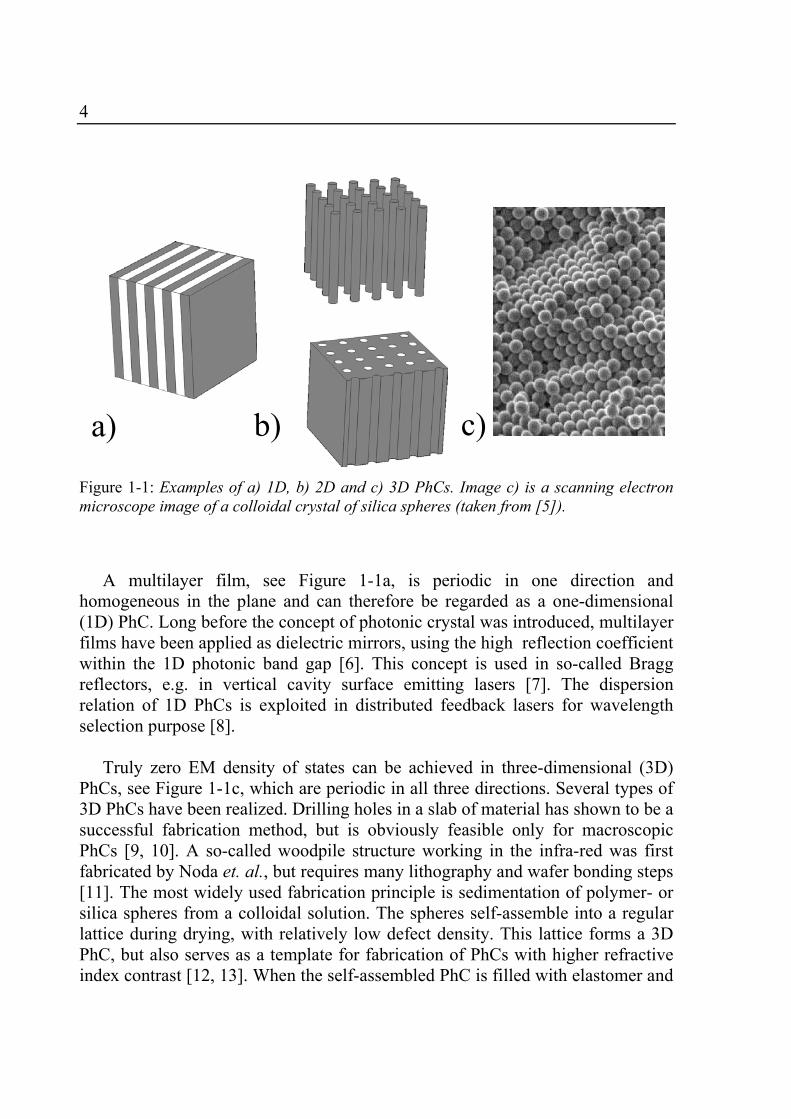
spectral position of the photonic band gap scales with the lattice constant a of the PhC. For a given lattice structure and refractive index contrast, the photonic band structure and transmission spectrum can therefore be presented in general form as a function of normalized frequency a/λ, in which λ is the free space wavelength. As in solid state physics, the opening of gaps occurs at the edge of the Brillouin zone where the wavelength in the medium is in the order of the lattice constant. Applications at optical wavelengths, e.g. for telecom or lighting, therefore require refractive index modulations with a period of a few hundred nanometer. Three main types of PhCs can be distinguished: 1D, 2D and 3D, referring to the number of spatial dimensions in which the refractive index is periodic, see Figure 1-1.
4
A multilayer film, see Figure 1-1a, is periodic in one direction and
homogeneous in the plane and can therefore be regarded as a one-dimensional (1D) PhC. Long before the concept of photonic crystal was introduced, multilayer films have been applied as dielectric mirrors, using the high reflection coefficient within the 1D photonic band gap [6]. This concept is used in so-called Bragg reflectors, e.g. in vertical cavity surface emitting lasers [7]. The dispersion relation of 1D PhCs is exploited in distributed feedback lasers for wavelength selection purpose [8].
Truly zero EM density of states can be achieved in three-dimensional (3D)
PhCs, see Figure 1-1c, which are periodic in all three directions. Several types of 3D PhCs have been realized. Drilling holes in a slab of material has shown to be a successful fabrication method, but is obviously feasible only for macroscopic PhCs [9, 10]. A so-called woodpile structure working in the infra-red was first fabricated by Noda et. al., but requires many lithography and wafer bonding steps [11]. The most widely used fabrication principle is sedimentation of polymer- or silica spheres from a colloidal solution. The spheres self-assemble into a regular lattice during drying, with relatively low defect density. This lattice forms a 3D PhC, but also serves as a template for fabrication of PhCs with higher refractive index contrast [12, 13]. When the self-assembled PhC is filled with elastomer and
Figure 1-1: Examples of a) 1D, b) 2D and c) 3D PhCs. Image c) is a scanning electron microscope image of a colloidal crystal of silica spheres (taken from [5]).
a) b) c)
5
the template is removed, it can be applied for taking fingerprints [14]. Two-dimensional (2D) PhCs are periodic in one selected plane and
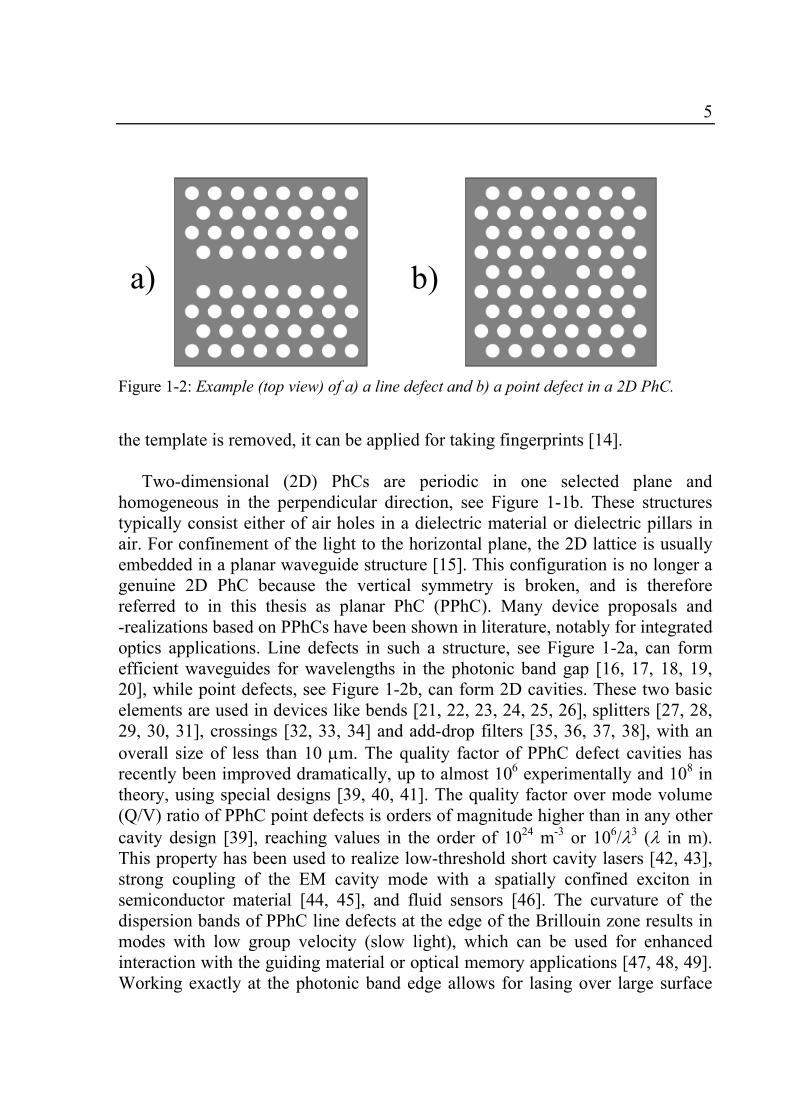
homogeneous in the perpendicular direction, see Figure 1-1b. These structures typically consist either of air holes in a dielectric material or dielectric pillars in air. For confinement of the light to the horizontal plane, the 2D lattice is usually embedded in a planar waveguide structure [15]. This configuration is no longer a genuine 2D PhC because the vertical symmetry is broken, and is therefore referred to in this thesis as planar PhC (PPhC). Many device proposals and -realizations based on PPhCs have been shown in literature, notably for integrated optics applications. Line defects in such a structure, see Figure 1-2a, can form efficient waveguides for wavelengths in the photonic band gap [16, 17, 18, 19, 20], while point defects, see Figure 1-2b, can form 2D cavities. These two basic elements are used in devices like bends [21, 22, 23, 24, 25, 26], splitters [27, 28, 29, 30, 31], crossings [32, 33, 34] and add-drop filters [35, 36, 37, 38], with an overall size of less than 10 µm. The quality factor of PPhC defect cavities has recently been improved dramatically, up to almost 106 experimentally and 108 in theory, using special designs [39, 40, 41]. The quality factor over mode volume (Q/V) ratio of PPhC point defects is orders of magnitude higher than in any other cavity design [39], reaching values in the order of 1024 m-3 or 106/λ3 (λ in m). This property has been used to realize low-threshold short cavity lasers [42, 43], strong coupling of the EM cavity mode with a spatially confined exciton in semiconductor material [44, 45], and fluid sensors [46]. The curvature of the dispersion bands of PPhC line defects at the edge of the Brillouin zone results in modes with low group velocity (slow light), which can be used for enhanced interaction with the guiding material or optical memory applications [47, 48, 49]. Working exactly at the photonic band edge allows for lasing over large surface
Figure 1-2: Example (top view) of a) a line defect and b) a point defect in a 2D PhC.
b) a)
6
areas [50]. It has also been shown, that PPhCs show anomalous refraction-like behavior in the vicinity of the photonic band edges [51, 52]. One consequence of this is the superprism phenomenon, which can be applied in wavelength filtering for wavelength division multiplexing (WDM) devices [53]. Another consequence is that PPhCs can exhibit negative refraction, which can be used for perfect near-field imaging [54].
1.2 Focus of this thesis In this thesis the focus is on PhCs that can be applied for photonic integrated
circuits (PICs) in long distance telecom applications at wavelengths near 1.55 µm. The base material system for active devices working at this wavelength is InP. The refractive index n of this material for λ = 1.55 µm (3.17 [56]), requires a ~ 400 nm. PPhCs are the natural choice for such applications because they can be integrated with planar laser structures and allow for much freedom in choice of crystal parameters and introduction of defects. Furthermore, they can in principle be fabricated with available patterning and etching techniques [57, 58, 59, 60, 61]. For compatibility with existing PICs, deeply etched- rather than membrane type PPhCs are investigated here. Hole type PPhCs are favorable over pillar type PPhCs, because they have a connected InP matrix and are thus expected to have more efficient guiding in the PhC region.
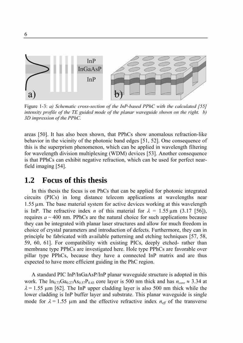
A standard PIC InP/InGaAsP/InP planar waveguide structure is adopted in this
work. The In0.73Ga0.27As0.57P0.43 core layer is 500 nm thick and has ncore ≈ 3.34 at λ = 1.55 µm [62]. The InP upper cladding layer is also 500 nm thick while the lower cladding is InP buffer layer and substrate. This planar waveguide is single mode for λ = 1.55 µm and the effective refractive index neff of the transverse
Figure 1-3: a) Schematic cross-section of the InP-based PPhC with the calculated [55] intensity profile of the TE guided mode of the planar waveguide shown on the right. b) 3D impression of the PPhC.
b) a)
7
electric (TE) guided mode is 3.25. The intensity profile of this mode is shown in the schematic cross-section of the PPhC in Figure 1-3a. For low out-of-plane loss it is crucial that the holes are deep enough to fully overlap with the vertical mode profile [63, 64]. A 3D representation of the PPhC is shown in Figure 1-3b.
A 2D photonic crystal is mirror symmetric with respect to every plane
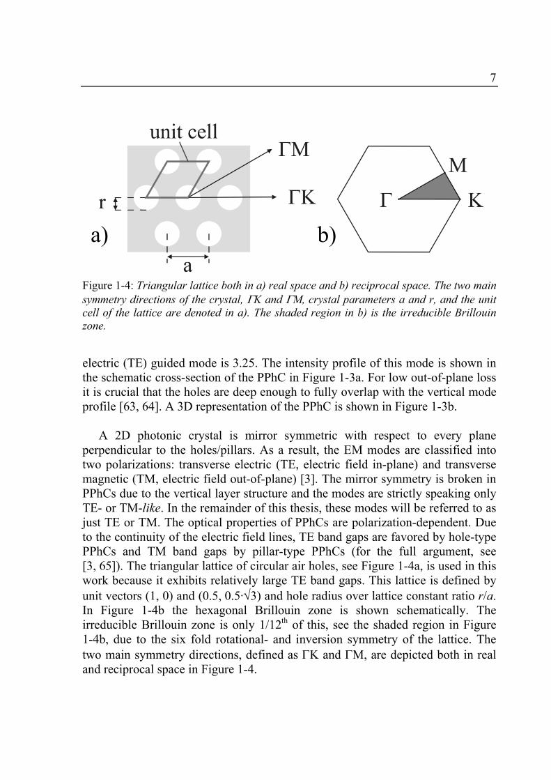
perpendicular to the holes/pillars. As a result, the EM modes are classified into two polarizations: transverse electric (TE, electric field in-plane) and transverse magnetic (TM, electric field out-of-plane) [3]. The mirror symmetry is broken in PPhCs due to the vertical layer structure and the modes are strictly speaking only TE- or TM-like. In the remainder of this thesis, these modes will be referred to as just TE or TM. The optical properties of PPhCs are polarization-dependent. Due to the continuity of the electric field lines, TE band gaps are favored by hole-type PPhCs and TM band gaps by pillar-type PPhCs (for the full argument, see [3, 65]). The triangular lattice of circular air holes, see Figure 1-4a, is used in this work because it exhibits relatively large TE band gaps. This lattice is defined by unit vectors (1, 0) and (0.5, 0.5·√3) and hole radius over lattice constant ratio r/a. In Figure 1-4b the hexagonal Brillouin zone is shown schematically. The irreducible Brillouin zone is only 1/12th of this, see the shaded region in Figure 1-4b, due to the six fold rotational- and inversion symmetry of the lattice. The two main symmetry directions, defined as ΓK and ΓM, are depicted both in real and reciprocal space in Figure 1-4.
Figure 1-4: Triangular lattice both in a) real space and b) reciprocal space. The two main symmetry directions of the crystal, ΓK and ΓM, crystal parameters a and r, and the unit cell of the lattice are denoted in a). The shaded region in b) is the irreducible Brillouin zone.
b) a)
8
For many applications in PICs it is crucial that the optical properties of PPhC components are externally tunable. Present WDM schemes have sub-nm channel spacing and the accuracy of the channel position must be even smaller to assure stable operation. This accuracy in the resonance of a PPhC cavity can not be achieved with current fabrication technology. For this kind of applications, static tuning, also called trimming, of the device characteristics is required. For modulation of an optical signal, dynamic PPhC tuning is needed. Current telecom networks, operating at 10 Gbit/s data rate per WDM channel, require tuning times < 100 ps. To change the optical properties of a PPhC, either the crystal geometry or the refractive index contrast has to be altered. The geometry can be changed by compression or expansion of the structure, which is difficult for InP-based PPhCs. The refractive index contrast can be changed by altering either the high- or the low index material. For the latter case, the air holes need to be filled with a material that has a tunable refractive index. This allows for tuning of the optical properties of the PPhC without compromising the properties of the InP that may be required for the application. Also it could be used to compensate changes in the refractive index of the InP, for instance to enhance the temperature stability of devices.
1.3 Contribution of this thesis to the field This thesis comprises the fabrication, characterization and infiltration of InP-
based hole-type PPhCs. The methods and materials used are described in detail in chapter 2 of this thesis. The main achievements that are new to the field are listed below.
1.3.1 Sidewall passivation The crucial process step in the fabrication of deeply etched PPhC is the final
etching of the high aspect-ratio holes in the planar waveguide layer structure. Several successful etching processes have been reported in the literature. Good results have been obtained with Cl2/Ar- [60] and Cl2-based [61] chemically assisted ion beam etching (CAIBE), Cl2/Ar-based electron cyclotron resonance (ECR) etching [59] and SiCl4-based inductively coupled plasma (ICP) etching [58]. In the present work, the etching is performed with ICP using Cl2 as the reactive component. Passivation of the sidewalls to obtain cylindrical hole-profiles is introduced by addition of O2 or N2 to the plasma chemistry. This concept is commonly exploited in etching of high aspect ratio structures in Si [66], but explicitly used here for the first time for the fabrication of InP based PPhCs. The major advantage of this chemistry is the increased window in the
9
parameter space in which the quality of the etched holes is acceptable, i.e. the holes are nearly cylindrical and sufficiently deep. This is an advantage when other structures, e.g. ridge access waveguides, need to be etched in the same run. The latter has proven to be particularly useful in this work. The etching results are presented in chapter 3.
1.3.2 End-fire transmission measurements in combination with loss parameter approach
In this thesis the PPhCs have been characterized by transmission measurements on finite crystal sections with no intentional defects, using an end-fire technique. Here, light from an external source is guided to and from the PPhC fields. This is in contrast with the internal light source (ILS) technique where the probe light originates from optically excited nanostructures like quantum wells or quantum dots that are incorporated in the material [67]. The latter technique has been successfully used in combination with a loss parameter approach [68] for assessment of the quality of GaAs-based [63] and InP-based [69] PPhCs. In this approach, the transmission measurements are fitted to 2D calculations in which the out-of-plane losses are simulated by introduction of a non-zero imaginary component of ε. The advantage of the end-fire technique is that it is generally applicable to any wavelength range in which the material is transparent. In ILS measurements of InP-based PPhCs, anomalously high transmission in the band gap is reported [69]. It will be shown in the remainder of this thesis, that > 30 dB transmission decrease in the gap can be observed with end-fire measurements. Although the end-fire technique is widely used, it is exploited here for the first time in combination with the loss parameter approach. An important result is that a considerable sidewall angle in the core layer does not lead to excessive losses, in contrast to what is commonly believed. Also it is shown that transmission through a PhC is possible by continuous diffraction of the light into allowed directions, even if the forward direction is forbidden. The optical measurements are described and analyzed in chapter 4.
1.3.3 Infiltration with polymer and liquid crystal The first proposal for PhC tuning with the low index material was done by
Bush and John [70]. They showed theoretically the possibility of opening and closing the band gap of a 3D PhC, using the tunability of infiltrated liquid crystals (LCs). Recently, liquid crystal infiltration has also been applied for tuning of PPhCs [71, 72, 73, 74, 75, 76]. In this thesis, PPhCs are filled with a solid polymer by monomer infiltration and in situ polymerization for the first time.
10
Both liquid crystals (LCs) and polymers have their advantages for tuning purposes and the material choice depends on the application. The main advantage of LCs is the large attainable refractive index change of typically ∆n = 0.2-0.3. On the other hand, < 1 ps tuning can in principle be achieved using optically non-linear polymers. Also, the solid nature of polymers allows for further (polymer) processing on top of the filled PhC and offers mechanical stability. In this thesis a simple, reliable and reproducible procedure for filling deeply etched PPhCs with polymer is presented. It is shown that the strong capillary forces exerted by a liquid inside the PhC holes allow for infiltration in ambient atmosphere. The polymer filling fraction is determined with optical measurements to be 80 %. The analysis of the filling experiments with both polymer and LCs is presented in chapter 5.

11
12
Chapter 2 Methods and materials
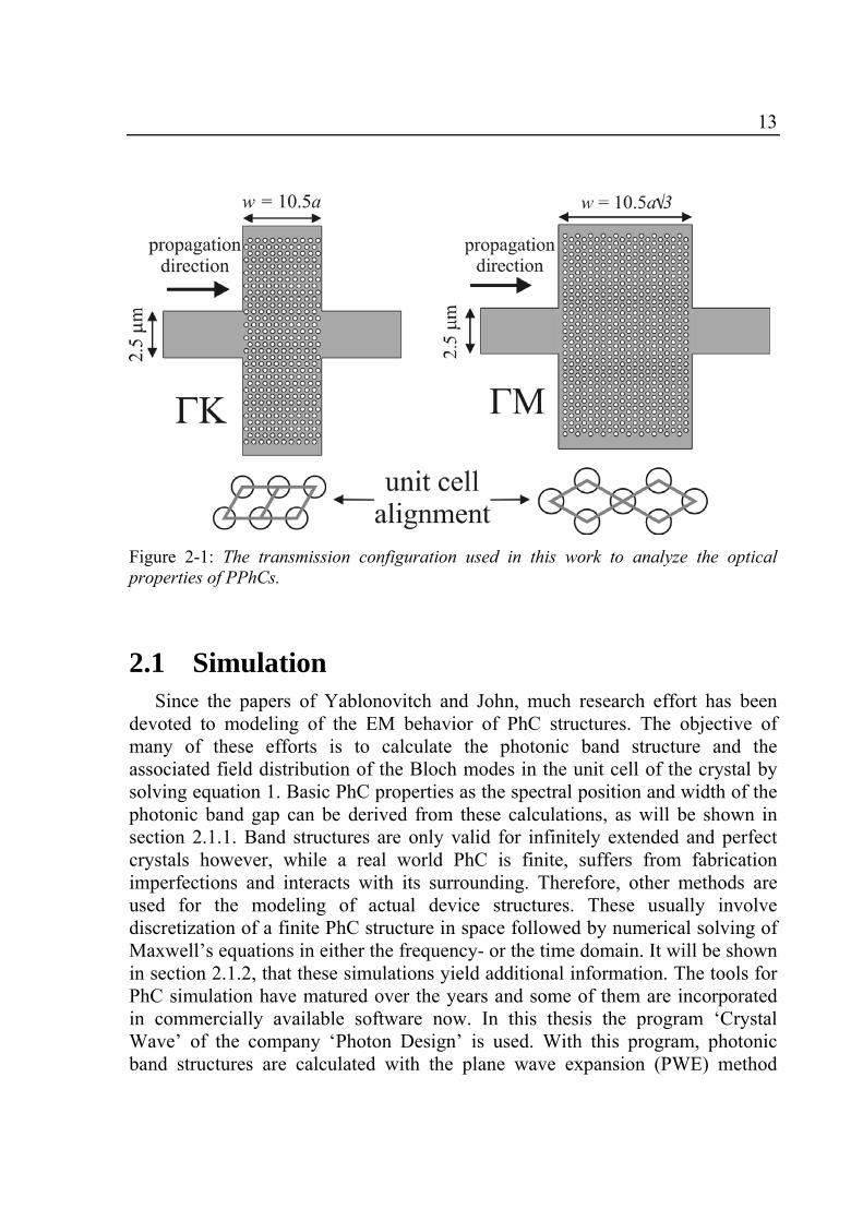
For optical simulation and -characterization, PhC sections without intentional defects are integrated with input- and output ridge waveguides in the transmission configuration as shown in Figure 2-1. The 2.5 µm wide ridges are formed by etching trenches on both sides and are aligned with either the ΓK- or the ΓM direction of the triangular lattice. The PhC section contains nine unit cells for the ΓK-direction and nine-and-a-half for the ΓM-direction, which are aligned as indicated in the figure. The center of the horizontally outer holes is placed on a distance 0.5⋅a (for ΓK, 0.5⋅√3a for ΓM) from the edge of the PhC section. The total distance between the waveguide ends is therefore 10.5⋅a for the ΓK- and 10.5⋅√3a for the ΓM-direction. In this region the light is not laterally guided but a significant fraction (>0.8) of the input light is collected by the output waveguide for the wavelength range considered here.
13
2.1 Simulation Since the papers of Yablonovitch and John, much research effort has been
devoted to modeling of the EM behavior of PhC structures. The objective of many of these efforts is to calculate the photonic band structure and the associated field distribution of the Bloch modes in the unit cell of the crystal by solving equation 1. Basic PhC properties as the spectral position and width of the photonic band gap can be derived from these calculations, as will be shown in section 2.1.1. Band structures are only valid for infinitely extended and perfect crystals however, while a real world PhC is finite, suffers from fabrication imperfections and interacts with its surrounding. Therefore, other methods are used for the modeling of actual device structures. These usually involve discretization of a finite PhC structure in space followed by numerical solving of Maxwell’s equations in either the frequency- or the time domain. It will be shown in section 2.1.2, that these simulations yield additional information. The tools for PhC simulation have matured over the years and some of them are incorporated in commercially available software now. In this thesis the program ‘Crystal Wave’ of the company ‘Photon Design’ is used. With this program, photonic band structures are calculated with the plane wave expansion (PWE) method
Figure 2-1: The transmission configuration used in this work to analyze the optical properties of PPhCs.
14
[77]. The EM behavior of actual device structures can be simulated in Crystal Wave using the finite difference time domain (FDTD) method [78] or with the frequency domain (FD) solver.
In principle, full 3D calculations are required for PPhCs, because the in-plane
and out-of-plane components of the electric field are not separable [68]. 3D calculations require long calculation times, while 2D calculations are feasible with current desktop computers. Because the vertical confinement of the planar waveguide used in this work is relatively low, the effective index approach can be used. In this approach, the PPhC is approximated by a purely 2D PhC with refractive index equal to neff, the effective index of the planar waveguide structure [79]. 2D simulations are then sufficient to model the 2D PhC. The effective index approach is applied in combination with both PWE and FDTD throughout this thesis.
In the 2D calculations, out-of plane components of the k-vector are not
accounted for. However, even perfect PPhCs with infinitely deep cylindrical holes exhibit so-called intrinsic losses for modes above the light line [80]. Deviations from the perfect crystal structure lead to so-called extrinsic losses [63, 64]. How to include losses in the 2D calculations is described in section 2.1.3.
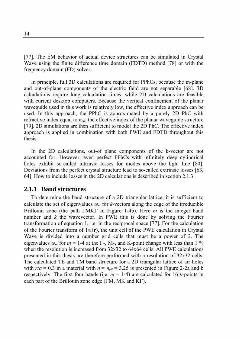
2.1.1 Band structures To determine the band structure of a 2D triangular lattice, it is sufficient to
calculate the set of eigenvalues ωm for k-vectors along the edge of the irreducible Brillouin zone (the path ΓMKΓ in Figure 1-4b). Here m is the integer band number and k the wavevector. In PWE this is done by solving the Fourier transformation of equation 1, i.e. in the reciprocal space [77]. For the calculation of the Fourier transform of 1/ε(r), the unit cell of the PWE calculation in Crystal Wave is divided into a number grid cells that must be a power of 2. The eigenvalues ωm for m = 1-4 at the Γ-, M-, and K-point change with less than 1 % when the resolution is increased from 32x32 to 64x64 cells. All PWE calculations presented in this thesis are therefore performed with a resolution of 32x32 cells. The calculated TE and TM band structure for a 2D triangular lattice of air holes with r/a = 0.3 in a material with n = neff = 3.25 is presented in Figure 2-2a and b respectively. The first four bands (i.e. m = 1-4) are calculated for 16 k-points in each part of the Brillouin zone edge (ΓM, MK and KΓ).
15
The so-called stop gaps for TE polarization between the m = 1 and m = 2 bands in the ΓK and ΓM direction are indicated in Figure 2-2a. They cover a different spectral region, because of the different periodicity in these crystal directions. The overlap of the stop gaps is indicated by the shaded region and covers frequency range a/λ = 0.221-0.287. No EM mode is available in this frequency region, which means that this is the TE photonic band gap of this particular crystal. As in semiconductors, the bands below and above the band gap have special names, dielectric band and air band respectively. These names refer
0.0
0.1
0.2
0.3
0.4
0.5TE
a/λ
lightline
ΓK stop gapΓM stop gap
band gap
Γ M K Γ
0.0
0.1
0.2
0.3
0.4
0.5TM
lightline
ΓM stop gap
a/λ
Γ M K Γ Figure 2-2: a) TE and b) TM band structure of a 2D triangular lattice of air holes with lattice parameter r/a = 0.3 calculated with Crystal Wave. The refractive index used is 3.25, such that these band diagrams represent the PPhCs fabricated in this work.
a)
b)
16
to the fact that the electric field of the mode is localized mostly in the dielectric material for the m = 1 band and more in the air holes for the m = 2 band. For a crystal with a = 400 nm and r = 120 nm, the band gap runs from 1394-1810 nm. The dashed line just above the m = 1 band is the light line of this configuration, which is just the m = 1 band of the 2D PhC formed by the perforated claddings [81]. Only the part of the band structure that lies below this light line represents truly guided modes. In Figure 2-2b it is visible that no band gap is present for TM polarized light, due to the degeneracy of the first two bands at the K-point. The relatively narrow stop gap for the ΓM direction is indicated in the figure.
Figure 2-2 represents the band structure for one particular value of r/a. In
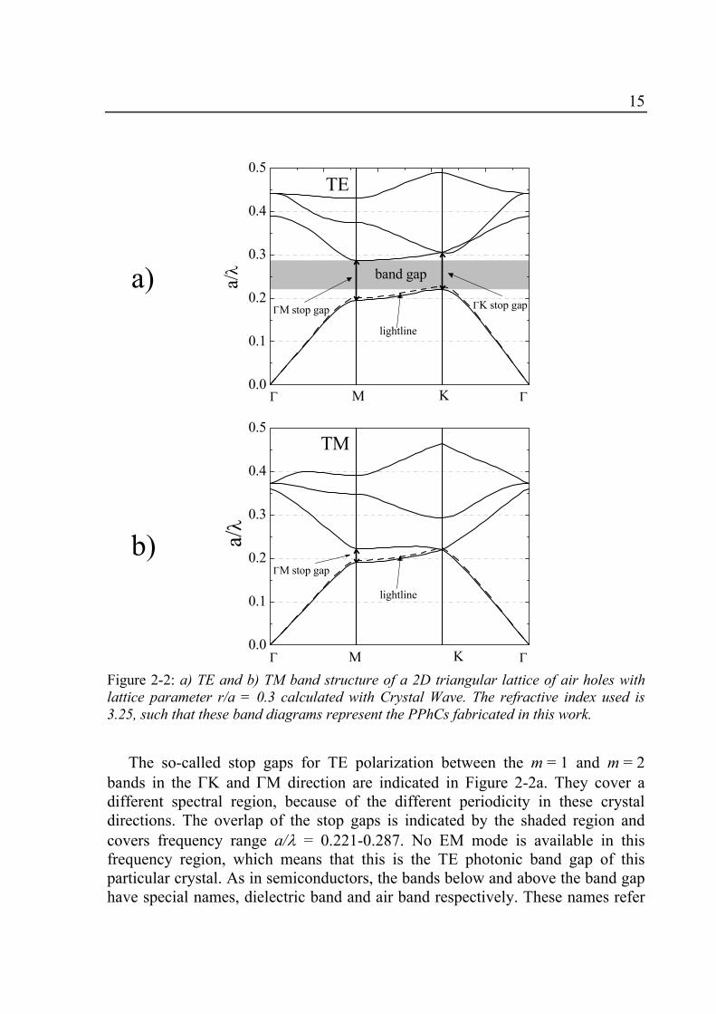
Figure 2-3 the grey areas represent the lowest photonic band gap as a function of r/a, ignoring higher order gaps in the graph. Such a graph is called a gap map. Only data for r/a ≤ 0.5 is shown in the figure, because the holes overlap for larger r/a. The TE band gap opens up at r/a = 0.15 and the relative gap width increases linearly up to r/a = 0.4. The center frequency of the gap increases with r/a, because the effective refractive index of the structure as a whole decreases. For r/a > 0.42 also a TM gap opens up, between the m = 2 and m = 3 band. Qualitatively this is because for large hole radii, the lattice resembles a lattice of pillars, although connected by thin veins [3]. A complete polarization independent gap is present for these high r/a values where the TM gap overlaps with the TE gap. The fabrication of such structures is a difficult task however, because small (sub 100 nm) features are left between the holes. Furthermore, the
0.0 0.1 0.2 0.3 0.4 0.5 0.60.0
0.1
0.2
0.3
0.4
0.5
0.6
0.7
a/λ
r/a0.0 0.1 0.2 0.3 0.4 0.5 0.6
0.0
0.1
0.2
0.3
0.4
0.5
0.6
0.7
a/λ
r/a0.0 0.1 0.2 0.3 0.4 0.5 0.6
0.0
0.1
0.2
0.3
0.4
0.5
0.6
0.7
a/λ
r/a
TETMboth
Figure 2-3: Gap map of a 2D PhC with n = 3.25. Calculations have been performed up to r/a = 0.5, where the holes touch one another. Higher order gaps are ignored here.
17
losses are high because most of the guiding material is removed. Therefore the focus here is on the more robust TE gap at moderate values of r/a.
2.1.2 Transmission spectra The transmission spectrum of the PhC configuration shown in Figure 2-1 is
simulated with FDTD. This means that the geometry is divided into a mesh of nodes, both in space and time. The field in each node is calculated from the field in neighboring nodes using a finite difference equivalent of Maxwell’s equations. For this purpose, the geometry is divided into a rectangular mesh that is matched to the triangular PhC lattice with a = 400 nm. A cell size of 10 x 10√3 nm proved to give sufficient resolution and is used for all FDTD calculations in this thesis. The time step for the evolution of the fields is related to the grid and equal to 1.4·10-17 s here. In the simulation, a Gaussian (in time) pulse with a central wavelength of 1.52 µm and bandwidth of 1 µm is excited in the input waveguide on the left. The in-plane field profile of the pulse is identical to the fundamental eigenmode of the 2.5 µm wide waveguide at the central wavelength. The optical signal is monitored by two Crystal Wave software sensors, one before and one after the PhC. The sensors register the computed optical power in the fundamental waveguide mode in the propagation direction of the pulse at these locations. Spectral information is obtained by Fourier transformation of the time-evolution of the signal. The duration of the calculation, the number of time steps, therefore determines the spectral resolution. The signal of the output sensor is divided by that of the input sensor to obtain the normalized transmission of the PhC.
18
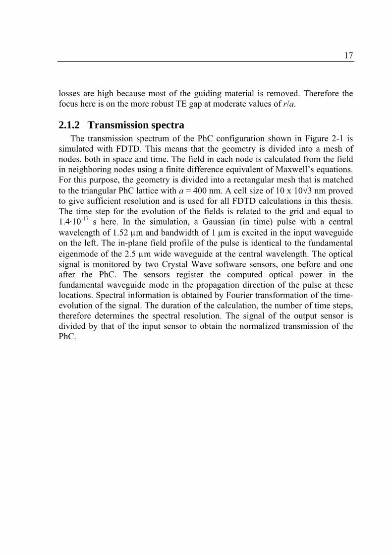
The transmission spectra for both symmetry directions are shown for TE and
TM polarization in Figure 2-4a and Figure 2-4b respectively. In Figure 2-4a, the positions of the TE stop gaps, as calculated with the PWE method, are indicated by vertical lines. These are in agreement with the regions where the transmission is decreased by several orders, down to 10-6, with respect to the pass bands. In the band gap the transmission is inhibited for both symmetry directions. The transmission level in the dielectric band is lower for the ΓM direction because of
0.15 0.20 0.25 0.30 0.35 0.4010-6
10-5
10-4
10-3
10-2
10-1
100
TE
ΓK ΓM
Tra
nsm
issi
on
a/λ
band gap
0.15 0.20 0.25 0.30 0.35 0.40
10-3
10-2
10-1
100
ΓK ΓM
TM
Tra
nsm
issi
on
a/λ
Figure 2-4: Calculated ΓK- and ΓM transmission spectra for the geometry of Figure 2-1 and a) TE- and b) TM polarization. The dashed vertical lines indicate the dielectric- and air band edge as calculated with the PWE method.
a)
b)
19
the larger w, and thus higher lateral losses. For ΓM the transmission levels in dielectric- and air band are calculated to be equal, but for ΓK the level is significantly lower in the air band. This could be due to a difference in grating-like diffraction. First order diffraction is possible for a/λ > (neff)-1 = 0.31 for the ΓM- and a/λ > (√3·neff)-1 = 0.18 for the ΓK direction [82, 83]. In the air band this is the case for both symmetry directions, but the diffraction efficiency is probably higher for ΓK at these a/λ values. The oscillations in the pass bands are due to Fabry-Pérot type interference between the boundaries of the PhC. At a/λ ~ 0.38 a second transmission minimum appears for both directions, although no stop gaps are visible in the band structure. This so-called pseudo gap is due to symmetry forbidden coupling of the ridge waveguide mode with the m = 3 band [15, 82, 83, 84].
The calculated narrow TM, ΓM stop gap is indicated by the vertical lines in
Figure 2-4b and is in agreement with the calculated transmission spectrum in the figure. In the ΓK direction, no stop gap is present, but a relatively broad transmission minimum is observed. This is again due to symmetry forbidden coupling, this time with the m = 2 band. At higher frequencies, also the symmetry of the m = 4 band results in a pseudo gap. For both ΓK and ΓM the transmission significantly drops just above the diffraction cut-off, at a/λ = 0.18 and 0.31 respectively.
2.1.3 Introduction of loss parameter ε'' The loss parameter approach was introduced by Benisty et. al. [68]. In this
approach, a fictitious absorption in the air holes is used to simulate out-of-plane optical losses in 2D calculations (here FDTD). This is realized by attributing a complex ε (ε = ε' + iε'' ) to the holes, while assuming the semiconductor to be lossless. The relation ε = n2 leads to the following relations between the real and imaginary components of n = n' + in'' and ε: 22 "'' nn −=ε and "'2" nn=ε . (2) In the Crystal Wave program losses are included by introduction of a power absorption coefficient α in the holes, while keeping n' constant. ε'' is related to α and n' by:
20
π
αλε2
n′=′′ . (3)
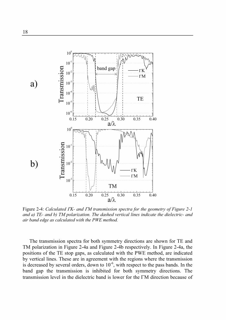
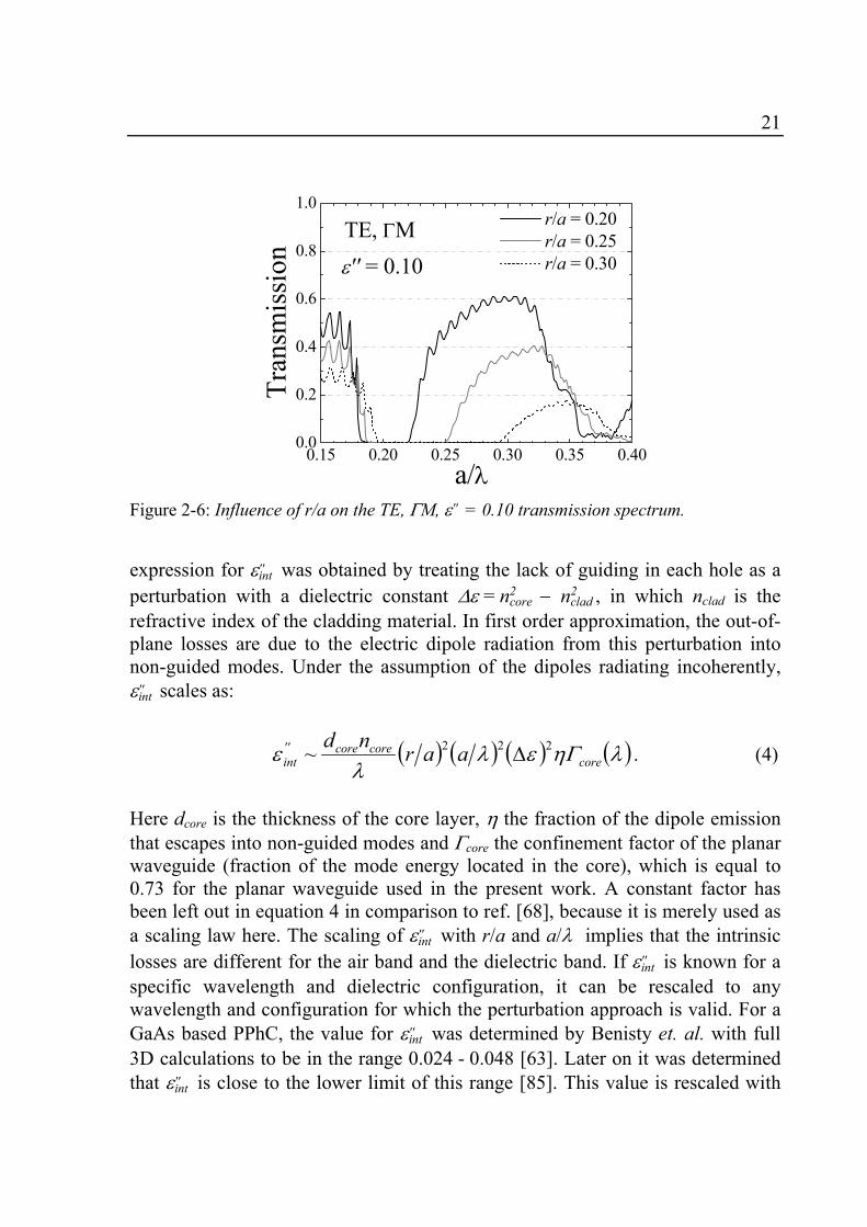
The influence of optical losses on the calculated TE, ΓM, r/a = 0.3 transmission spectrum is shown in Figure 2-5 on linear transmission scale. The most important changes in the spectrum upon increase of the loss are the decrease of the transmission level, notably in the air band, and damping of the Fabry-Pérot fringes. The difference in sensitivity to ε'' of the dielectric- and air band arises from the sampling of the holes by the respective Bloch modes. The TM spectrum is less sensitive to the loss parameter than the TE spectrum, because the Bloch mode is concentrated more in the high dielectric for this polarization, specifically in the air band. The gray line in Figure 2-5 represents the case ε'' = εint'' , see section 2.1.4, and shows already significant decrease of the transmission level. In Figure 2-6, the influence of r/a on the TE, ΓM, ε'' = 0.10 transmission spectrum is shown. Larger r/a values lead to lower transmission levels, due to the larger absorbing area in the simulation. The influence of r/a on the stop gap width, following Figure 2-3, is also apparent.
2.1.4 Loss mechanisms: εint'' , εext'' and εhole'' The loss parameter ε'' is the sum of an intrinsic contribution εint'' , due to the perturbation of the vertical waveguide structure in the air holes, and an extrinsic contribution εext'' , due to fabrication imperfections. In ref. [68], a semi-quantitative
0.15 0.20 0.25 0.30 0.35 0.400.0
0.2
0.4
0.6
0.8
1.0
r/a = 0.30TE, ΓM ε'' = 0
ε'' = 0.024 (ε''int)
ε'' = 0.10
Tra
nsm
issi
on
a/λ Figure 2-5: Influence of ε'' on the TE, GM, r/a = 0.30 transmission spectrum.
21
expression for εint'' was obtained by treating the lack of guiding in each hole as a perturbation with a dielectric constant ∆ε = ncore
2 − nclad2 , in which nclad is the
refractive index of the cladding material. In first order approximation, the out-of-plane losses are due to the electric dipole radiation from this perturbation into non-guided modes. Under the assumption of the dipoles radiating incoherently, εint'' scales as:
( ) ( ) ( ) ( )λΓηελλ
ε corecorecore''
int aarnd 222~ ∆ . (4)
Here dcore is the thickness of the core layer, η the fraction of the dipole emission that escapes into non-guided modes and Γcore the confinement factor of the planar waveguide (fraction of the mode energy located in the core), which is equal to 0.73 for the planar waveguide used in the present work. A constant factor has been left out in equation 4 in comparison to ref. [68], because it is merely used as a scaling law here. The scaling of εint'' with r/a and a/λ implies that the intrinsic losses are different for the air band and the dielectric band. If εint'' is known for a specific wavelength and dielectric configuration, it can be rescaled to any wavelength and configuration for which the perturbation approach is valid. For a GaAs based PPhC, the value for εint'' was determined by Benisty et. al. with full 3D calculations to be in the range 0.024 - 0.048 [63]. Later on it was determined that εint'' is close to the lower limit of this range [85]. This value is rescaled with
0.15 0.20 0.25 0.30 0.35 0.400.0
0.2
0.4
0.6
0.8
1.0
ε'' = 0.10TE, ΓM r/a = 0.20
r/a = 0.25 r/a = 0.30
Tra
nsm
issi
on
a/λ Figure 2-6: Influence of r/a on the TE, ΓM, ε'' = 0.10 transmission spectrum.
22
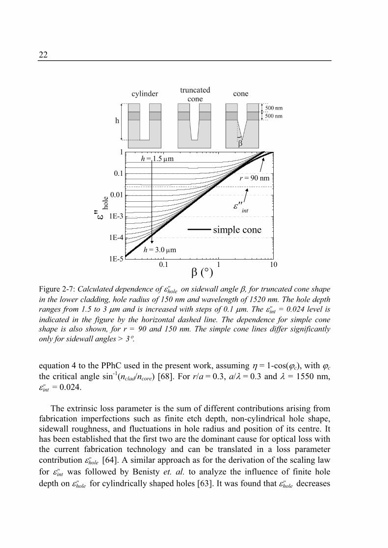
equation 4 to the PPhC used in the present work, assuming η = 1-cos(ϕc), with ϕc the critical angle sin-1(nclad/ncore) [68]. For r/a = 0.3, a/λ = 0.3 and λ = 1550 nm, εint'' = 0.024.
The extrinsic loss parameter is the sum of different contributions arising from fabrication imperfections such as finite etch depth, non-cylindrical hole shape, sidewall roughness, and fluctuations in hole radius and position of its centre. It has been established that the first two are the dominant cause for optical loss with the current fabrication technology and can be translated in a loss parameter contribution εhole'' [64]. A similar approach as for the derivation of the scaling law for εint'' was followed by Benisty et. al. to analyze the influence of finite hole depth on εhole'' for cylindrically shaped holes [63]. It was found that εhole'' decreases
0.1 1 101E-5
1E-4
1E-3
0.01
0.1
1
ε''int
r = 90 nm
h = 3.0 µm
simple cone
β (°)
ε''ho
le
h = 1.5 µm
Figure 2-7: Calculated dependence of εhole'' on sidewall angle β, for truncated cone shape in the lower cladding, hole radius of 150 nm and wavelength of 1520 nm. The hole depth ranges from 1.5 to 3 µm and is increased with steps of 0.1 µm. The εint'' = 0.024 level is indicated in the figure by the horizontal dashed line. The dependence for simple cone shape is also shown, for r = 90 and 150 nm. The simple cone lines differ significantly only for sidewall angles > 3°.
23
exponentially with etch depth, due to the exponential decrease of the guided mode intensity in the lower cladding. In first approach the focus in the fabrication process development should therefore be at maximal hole depth. Ferrini et. al. obtained an analytical expression for this case [64], which can be written for hole depth h as:
( ) ( ) decayh
cladclad''hole Lrnn λΓ
λπε 2
3
223 13
8 −= . (5)
Here Γh is the fraction of the mode energy below a distance h from the top
surface and Ldecay a characteristic decay length of the mode intensity in the lower cladding. Equation 5 shows that εhole'' scales with r2/λ3 and therefore it is higher in the air band than in the dielectric band for equal hole depth. The analysis was extended by Ferrini et. al. to holes with (truncated) cylindroconical profile, a more realistic shape after etching [64, 86]. This was performed under the assumption that the cylindrical section of the hole extends at least to the bottom of the core layer. Following the approach in refs. 64 and 86, the dependence on sidewall angle β for increasing etch depth was calculated for the three layer heterostructure used in this thesis1. The sidewall angle is defined here as the deviation from the vertical. The result for λ = 1520 nm and r = 150 nm, with 1.5 µm < h < 3 µm in steps ∆h = 0.1 µm, is shown in Figure 2-7. For r/a = 0.3, this is in the air band of the transmission spectrum. Above a certain sidewall angle, which depends on the hole depth, the truncated hole shape is simply conical. The simple cone lines for r = 90 and 150 nm are also shown in the figure and differ significantly only for β > 3°. Two regimes are distinctly visible in Figure 2-7. For small β, the truncated cone line saturates to a depth dependent εhole'' value that is lower than εint'' for h > 2 µm. For large β, εhole'' is primarily determined by the cone angle and εhole'' < εint'' only for β < 0.8°. This highlights the demand for nearly cylindrical shape of the holes, particularly in the part just below the core layer [64]. Thus, in the optimization of the etching process, both hole depth and sidewall angle need to be considered for significant reduction of the optical loss.
1 For these calculations the original Matlab-files developed by dr. R. Ferrini were used.
24
2.2 Process development
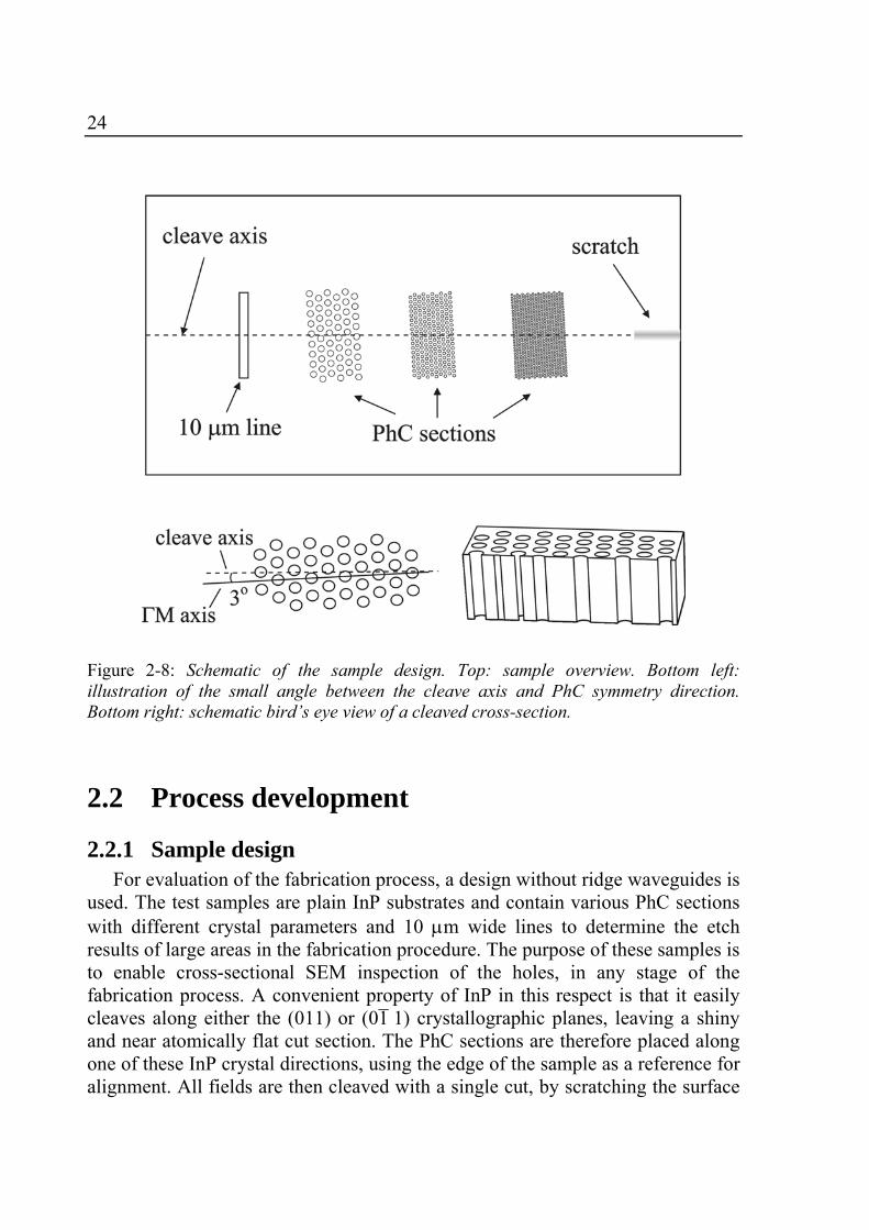
2.2.1 Sample design For evaluation of the fabrication process, a design without ridge waveguides is
used. The test samples are plain InP substrates and contain various PhC sections with different crystal parameters and 10 µm wide lines to determine the etch results of large areas in the fabrication procedure. The purpose of these samples is to enable cross-sectional SEM inspection of the holes, in any stage of the fabrication process. A convenient property of InP in this respect is that it easily cleaves along either the (011) or (01̄ 1) crystallographic planes, leaving a shiny and near atomically flat cut section. The PhC sections are therefore placed along one of these InP crystal directions, using the edge of the sample as a reference for alignment. All fields are then cleaved with a single cut, by scratching the surface
Figure 2-8: Schematic of the sample design. Top: sample overview. Bottom left: illustration of the small angle between the cleave axis and PhC symmetry direction. Bottom right: schematic bird’s eye view of a cleaved cross-section.
25
at the edge of the sample with a diamond scriber and applying force onto the sample next to the scratch. The symmetry axis of the PhC, either ΓK or ΓM, is tilted under a small angle (~3°) with respect to the cleavage so that a different part of the cross-section is visible for each hole. See Figure 2-8 for a schematic overview of the sample design.
2.2.2 Layer structure The planar waveguide structure is grown on top of a (100) oriented epi-ready
2 inch InP wafer with metal organic chemical vapor deposition (MOCVD). A 1000 nm thick InP buffer layer is grown on the InP substrate, followed by the lattice matched 500 nm thick In0.73Ga0.27As0.57P0.43 core layer and the 500 nm thick InP upper cladding. The peak photoluminescence emission of the quaternary material is at 1265 ± 5 nm. After the MOCVD growth a SiNx hard mask is deposited on the full wafer by plasma enhanced chemical vapor deposition (PECVD). The thickness and average refractive index of this layer were measured with an ellipsometer to be ~370 nm and 2.0 (at visible wavelengths) respectively, giving the surface a green color. The wafer was then cleaved into nine pieces of approximately 16x16 mm2. A layer of ZEP-520A (ZEON) electron beam (e-beam) resist solution in anisole was deposited onto the individual pieces by spin coating at 5000 rpm for 50 seconds. The layer was baked on a hotplate for 120 seconds to evaporate the solvent, leaving a 320 nm thick resist layer.
2.2.3 E-beam lithography The 2D PhC patterns and the ridge waveguides are defined in the ZEP layer
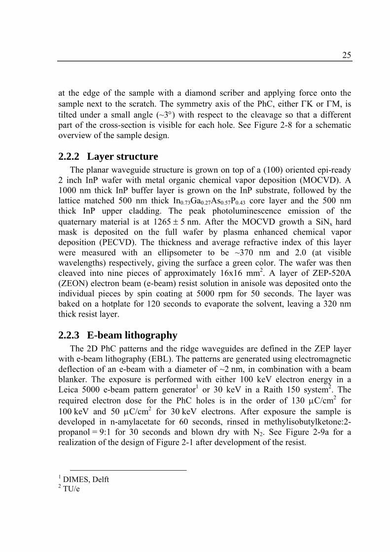
with e-beam lithography (EBL). The patterns are generated using electromagnetic deflection of an e-beam with a diameter of ~2 nm, in combination with a beam blanker. The exposure is performed with either 100 keV electron energy in a Leica 5000 e-beam pattern generator1 or 30 keV in a Raith 150 system2. The required electron dose for the PhC holes is in the order of 130 µC/cm2 for 100 keV and 50 µC/cm2 for 30 keV electrons. After exposure the sample is developed in n-amylacetate for 60 seconds, rinsed in methylisobutylketone:2-propanol = 9:1 for 30 seconds and blown dry with N2. See Figure 2-9a for a realization of the design of Figure 2-1 after development of the resist.
1 DIMES, Delft 2 TU/e
26
The actual developed pattern deviates from the design because of the so-called proximity effect, which is due to scattering of the electrons in the material. These electrons travel through the resist and cause parasitic exposure outside the area that was directly exposed by the electron beam. For 100 keV, this causes a rather uniform background dose over a range of ~15 µm, while for 30 keV the range is limited to ~2 µm and the gradient in the dose is much larger [87, 88, 89]. In general, feature sizes are larger than designed due to the proximity effect. This is in particular the case for the PhC holes in the design of Figure 2-1, because of the proximity of the large exposed areas that define the waveguides, see Figure 2-9b. This can be corrected by either adjustment of the dose distribution or decrease of the hole diameter in the design. In this work, the latter option was used. From dose tests with the 100 keV e-beam for the actual device pattern, so including the large areas for definition of the waveguides, using SEM inspection from top it was determined that the radius of the holes should be designed ~30 nm smaller for the desired r/a-value of 0.3.
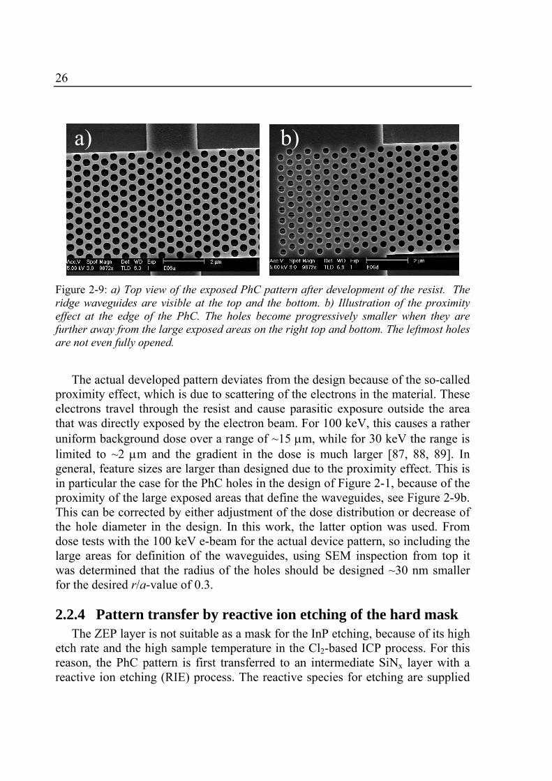
2.2.4 Pattern transfer by reactive ion etching of the hard mask The ZEP layer is not suitable as a mask for the InP etching, because of its high
etch rate and the high sample temperature in the Cl2-based ICP process. For this reason, the PhC pattern is first transferred to an intermediate SiNx layer with a reactive ion etching (RIE) process. The reactive species for etching are supplied
Figure 2-9: a) Top view of the exposed PhC pattern after development of the resist. The ridge waveguides are visible at the top and the bottom. b) Illustration of the proximity effect at the edge of the PhC. The holes become progressively smaller when they are further away from the large exposed areas on the right top and bottom. The leftmost holes are not even fully opened.
a) b)
27
by a plasma that is generated above the sample in a cylindrical vacuum chamber by capacitive coupling, see Figure 2-10a for a schematic overview. Radiofrequency (RF) power is applied to the bottom electrode plate. This generates an oscillating electric field in the chamber, which ionizes and dissociates the gas that is introduced into the chamber by inlets at the top. The electrons in the plasma are much more mobile compared to the more massive ions and collide with the electrodes driven by the RF field. The bottom electrode is electrically isolated from the rest of the grounded chamber and acquires a net negative charge by the absorbed electrons. The resulting DC bias voltage Vbias is typically in the order of a few hundred volts and accelerates the positive ions towards the sample. The plasma potential is slightly positive, in the order of several tens of volts, because of the loss of electrons. The chemical etching process is enhanced by the ion bombardment, which results in anisotropic etching profiles.
CHF3 chemistry is used for the pattern transfer to the SiNx-layer1. With a gas
flow of 60 sccm CHF3, 50 W RF power and chamber pressure p of 2.0 Pa, the induced Vbias = -(250-350) V and the large area etch rate is 20 nm/min for the SiNx and 15 nm/min for the ZEP. The etch rate is lower for the PhC holes, because of gas depletion at the bottom. This phenomenon depends on the aspect ratio of the feature (depth divided by lateral width) and is commonly called RIE lag [90]. The required time to open the smallest holes, with a diameter of ~160 nm, is therefore increased with a factor of 1.5 compared to large areas. The
1 Performed with the Plasmalab 100 RIE system from Oxford Instruments
Figure 2-10: a) Schematic of the RIE system b) Cross-sectional SEM view of the sample after RIE of the SiNx.
b) a)
28
etch rate is also influenced by the size of the sample. The values given are valid only for a sample size of approximately 15x15 mm2. For a full 2 inch wafer the etch rates decrease with a factor of 1.5 due to loading effects [90]. A cross-sectional SEM view of a PhC pattern in the SiNx mask is shown in Figure 2-10b. After the RIE pattern transfer, the residual ZEP is removed with an O2 plasma in a barrel etcher.
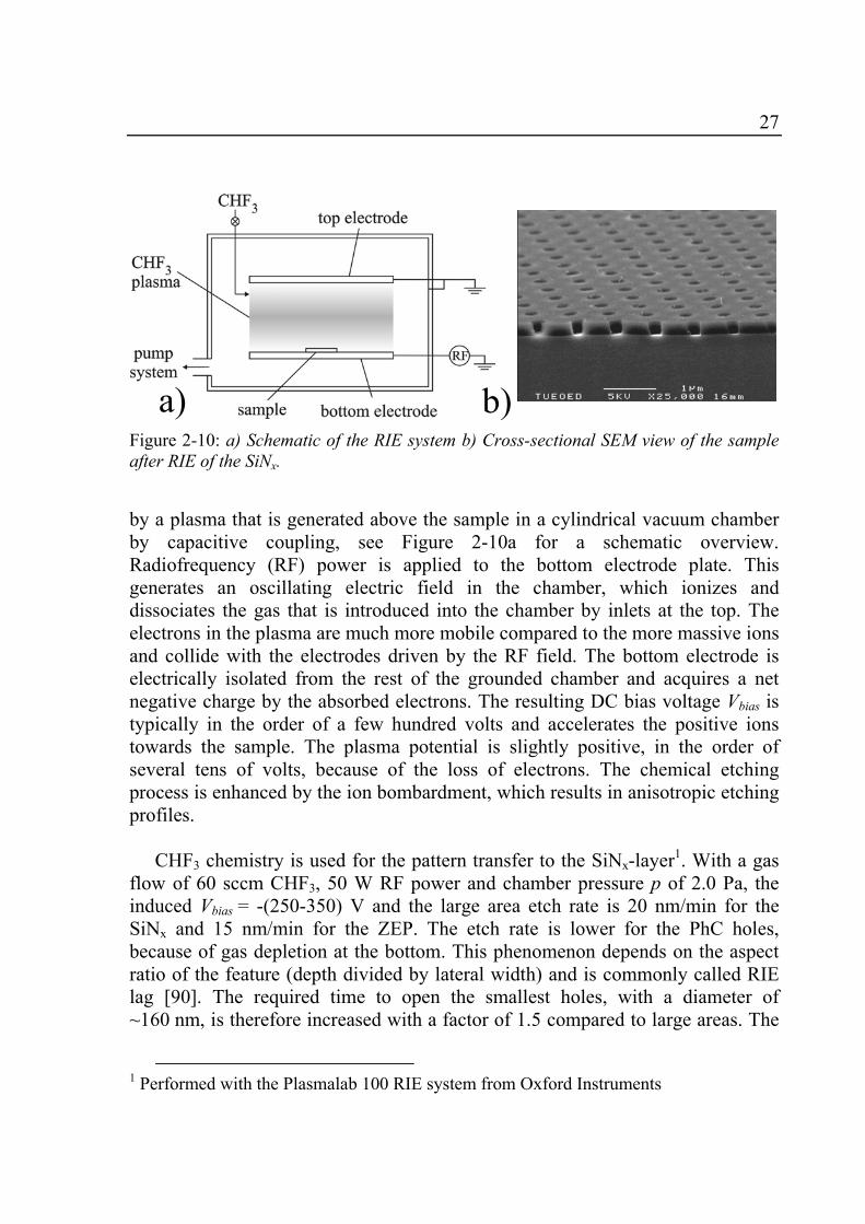
2.2.5 ICP etching The PhC holes are etched in the InP with ICP etching, using the SiNx as
patterned masking layer. The etching plasma is generated in a cylindrical vacuum chamber by inductive coupling, see Figure 2-11 for a schematic overview of the system. RF power (Ps) is applied to a helical coil outside the chamber, which induces an oscillating magnetic field along the coil axis. This in turn produces azimuthal electric fields that ionize the gas that is fed through the coil. The plasma expands to the lower part of the chamber, where the sample is located on a plate electrode. This electrode is powered by a separate RF source (with plate power Pp) to produce a bias voltage. The bias voltage and plasma density are
Figure 2-11: Schematic of the ICP etching system.
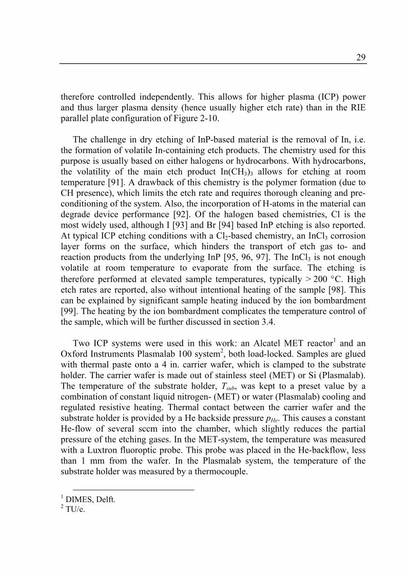
29
therefore controlled independently. This allows for higher plasma (ICP) power and thus larger plasma density (hence usually higher etch rate) than in the RIE parallel plate configuration of Figure 2-10.
The challenge in dry etching of InP-based material is the removal of In, i.e.
the formation of volatile In-containing etch products. The chemistry used for this purpose is usually based on either halogens or hydrocarbons. With hydrocarbons, the volatility of the main etch product In(CH3)3 allows for etching at room temperature [91]. A drawback of this chemistry is the polymer formation (due to CH presence), which limits the etch rate and requires thorough cleaning and pre-conditioning of the system. Also, the incorporation of H-atoms in the material can degrade device performance [92]. Of the halogen based chemistries, Cl is the most widely used, although I [93] and Br [94] based InP etching is also reported. At typical ICP etching conditions with a Cl2-based chemistry, an InCl3 corrosion layer forms on the surface, which hinders the transport of etch gas to- and reaction products from the underlying InP [95, 96, 97]. The InCl3 is not enough volatile at room temperature to evaporate from the surface. The etching is therefore performed at elevated sample temperatures, typically > 200 °C. High etch rates are reported, also without intentional heating of the sample [98]. This can be explained by significant sample heating induced by the ion bombardment [99]. The heating by the ion bombardment complicates the temperature control of the sample, which will be further discussed in section 3.4.
Two ICP systems were used in this work: an Alcatel MET reactor1 and an
Oxford Instruments Plasmalab 100 system2, both load-locked. Samples are glued with thermal paste onto a 4 in. carrier wafer, which is clamped to the substrate holder. The carrier wafer is made out of stainless steel (MET) or Si (Plasmalab). The temperature of the substrate holder, Tsub, was kept to a preset value by a combination of constant liquid nitrogen- (MET) or water (Plasmalab) cooling and regulated resistive heating. Thermal contact between the carrier wafer and the substrate holder is provided by a He backside pressure pHe. This causes a constant He-flow of several sccm into the chamber, which slightly reduces the partial pressure of the etching gases. In the MET-system, the temperature was measured with a Luxtron fluoroptic probe. This probe was placed in the He-backflow, less than 1 mm from the wafer. In the Plasmalab system, the temperature of the substrate holder was measured by a thermocouple.
1 DIMES, Delft. 2 TU/e.
30
A Langmuir probe was used to measure the ion current density, J, to the
sample and the plasma potential, Vp. The value for the ion current density can be used to determine the ion yield (atoms removed per incoming ion) by the relation:
JeRN
MMY A
PIn
InP
+=
ρ. (6)
Here ρInP is the density of InP (4.81⋅103 kg/m3 ([100], page 12-98)), Mx the molar mass of either In (0.115 kg) or P (0.031 kg) ([100], page 1-13), NA Avogadro’s number, R the measured etch rate, and e the electronic charge. It is assumed here that the ions are singly charged. If ions with higher charge are also present, the yield will be underestimated by equation 6. The ions incident on the surface are accelerated over a total voltage that is the difference of Vp and Vbias. The ion energy, Eion, is therefore equal to Vp - Vbias for singly charged ions, in units of eV.
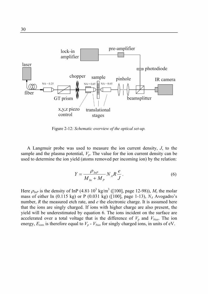
Figure 2-12: Schematic overview of the optical set-up.
31
2.3 Optical characterization
2.3.1 Optical set-up A schematic overview of the optical set-up for characterization of the
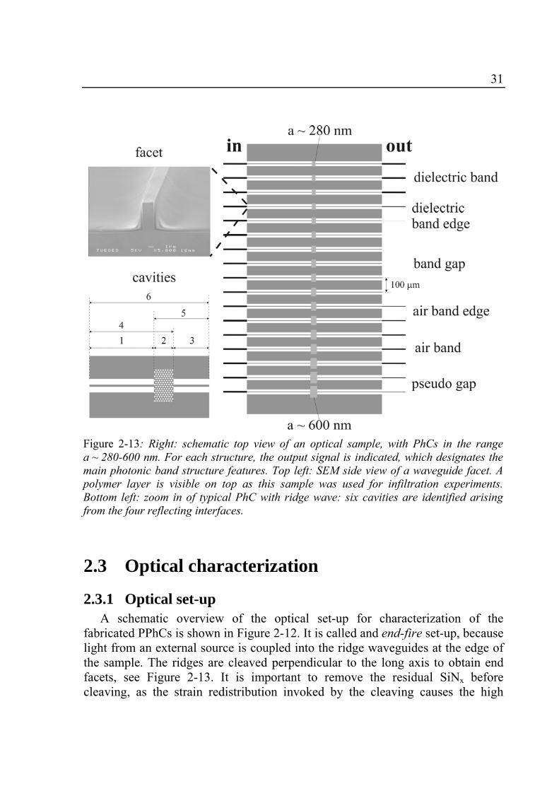
fabricated PPhCs is shown in Figure 2-12. It is called and end-fire set-up, because light from an external source is coupled into the ridge waveguides at the edge of the sample. The ridges are cleaved perpendicular to the long axis to obtain end facets, see Figure 2-13. It is important to remove the residual SiNx before cleaving, as the strain redistribution invoked by the cleaving causes the high
Figure 2-13: Right: schematic top view of an optical sample, with PhCs in the range a ~ 280-600 nm. For each structure, the output signal is indicated, which designates the main photonic band structure features. Top left: SEM side view of a waveguide facet. A polymer layer is visible on top as this sample was used for infiltration experiments. Bottom left: zoom in of typical PhC with ridge wave: six cavities are identified arising from the four reflecting interfaces.
32
aspect ratio ridges to break. The external light source is a Tunics BT diode laser with external cavity that is
tunable in wavelength from 1470 nm to 1570 nm with a resolution of 1 pm. The polarization-controlled output light with a power of 1 mW is radiated to free space from a polarization maintaining (PM) fiber and collimated with a microscope objective with a numerical aperture (NA) of 0.25. The polarization output of the PM fiber is set to TE or TM with respect to the sample. The polarization of the light is further defined with a Glan-Thompson prism. The collimated beam is chopped at a modulation frequency of 310 Hz to allow phase-sensitive detection via a lock-in technique and focused at the end facets by microscope objectives with NA = 0.65. The Gaussian beam waist at the input-facet is estimated to be ~4 µm, which implies a coupling loss of ~5 dB with the fundamental waveguide mode1. The first order mode of the waveguide is not excited because it is anti-symmetric with respect to the Gaussian beam profile. The second order mode (highest order for a waveguide width of 2.5 µm) will be excited, but with an intensity that is calculated to be 17 times lower than for the fundamental mode1. Also it will scatter more at waveguide imperfections than the fundamental mode. For these reasons only the fundamental mode is regarded in the remainder of this thesis. The sample and in- and out-coupling objectives are positioned on translational stages with differential screws for alignment in three directions. To optimize the position of the beam waist with respect to the waveguiding layer, the input objective has translational piezo control in three directions. This optimization is done by maximizing the detector signal. The focal point of the objectives is wavelength dependent, which causes transmission loss up to 50 % at the boundaries of the wavelength range, when the signal is optimized at λ = 1520 nm. Therefore each crystal is measured in two wavelength intervals: 1470-1520 nm and 1520-1570 nm, with signal optimization at λ = 1495 and 1545 nm respectively. This reduces the transmission loss to less than 10 %. In the stop gap, the low signal only allows optimization of the lateral alignment. Structures that have transmission in the stop gap for the entire tuning range of the laser are laterally aligned at λ = 1520 nm and measured in one interval. If signal optimization is not possible at λ = 1495 nm (1545 nm), because it is below the stray light level for that wavelength, the crystal is measured for the entire wavelength range after signal optimization at λ = 1545 nm (1495 nm). A lens-
1 Calculated from the overlap of the eigenmodes of the ridge waveguide with the Gaussian beam waist. Performed by L. Augustin, Optoelectronic Devices (OED) group, faculty of Electrical Engineering, TU/e.
33
pinhole system after the output objective is used to spatially filter the transmitted signal and reduce the contribution of stray light. The signal is detected with an InGaAs photodiode in combination with a lock-in amplifier. An infrared camera is used to image the output facet for alignment purposes.
Lithographic tuning [15, 101] is employed to cover the photonic band gap
with the limited tuning range of the laser. This means that transmission spectra of photonic crystal structures with various a, ranging from 250-600 nm, are measured with 1 nm wavelength steps. The trenches that define the ridge waveguides are 20 µm wide at both sides and the distance between the structures is 100 µm. The total length of the waveguides is 1-4 mm, with usually a similar segment on either side of the PhC. For normalization and alignment purposes several uninterrupted ridge waveguides, i.e. without PhC section, are included in between the PhCs. The total number of structures on a completed single sample with both ΓK- and ΓM oriented crystals is ~50 and the size of the chip is typically 2 x 8 mm2. A schematic overview of the sample is shown in Figure 2-13. The six cavities that may lead to Fabry-Pérot oscillations in the measured spectrum are also indicated in the figure.
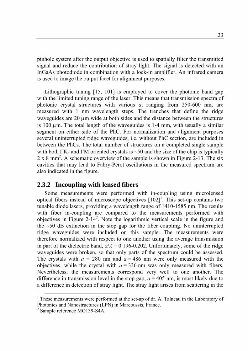
2.3.2 Incoupling with lensed fibers Some measurements were performed with in-coupling using microlensed
optical fibers instead of microscope objectives [102]1. This set-up contains two tunable diode lasers, providing a wavelength range of 1410-1585 nm. The results with fiber in-coupling are compared to the measurements performed with objectives in Figure 2-142. Note the logarithmic vertical scale in the figure and the ~50 dB extinction in the stop gap for the fiber coupling. No uninterrupted ridge waveguides were included on this sample. The measurements were therefore normalized with respect to one another using the average transmission in part of the dielectric band, a/λ = 0.196-0.202. Unfortunately, some of the ridge waveguides were broken, so that only parts of the spectrum could be assessed. The crystals with a = 280 nm and a = 486 nm were only measured with the objectives, while the crystal with a = 336 nm was only measured with fibers. Nevertheless, the measurements correspond very well to one another. The difference in transmission level in the stop gap, a = 405 nm, is most likely due to a difference in detection of stray light. The stray light arises from scattering in the
1 These measurements were performed at the set-up of dr. A. Talneau in the Laboratory of Photonics and Nanostructures (LPN) in Marcoussis, France. 2 Sample reference MO139-S4A.
34
sample, because even in the stop gap, the signal drops several orders when the laser is deliberately turned off. Probably less stray light is captured at the output by the microlensed fiber compared to the microscope objective, because the physical aperture of the latter is orders of magnitude larger. No TE/TM conversion is induced in the PPhC by the vertical waveguide structure here, because it is symmetrical around the core [103]. However a small polarization conversion due to the slightly conical shape of the holes cannot be ruled out.
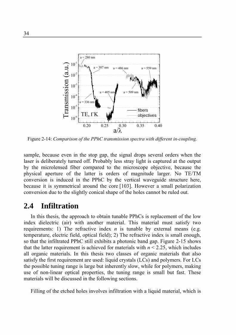
2.4 Infiltration In this thesis, the approach to obtain tunable PPhCs is replacement of the low
index dielectric (air) with another material. This material must satisfy two requirements: 1) The refractive index n is tunable by external means (e.g. temperature, electric field, optical field); 2) The refractive index is small enough, so that the infiltrated PPhC still exhibits a photonic band gap. Figure 2-15 shows that the latter requirement is achieved for materials with n < 2.25, which includes all organic materials. In this thesis two classes of organic materials that also satisfy the first requirement are used: liquid crystals (LCs) and polymers. For LCs the possible tuning range is large but inherently slow, while for polymers, making use of non-linear optical properties, the tuning range is small but fast. These materials will be discussed in the following sections.
Filling of the etched holes involves infiltration with a liquid material, which is
0.20 0.25 0.30 0.35 0.4010-6
10-5
10-4
10-3
10-2
10-1
a = 336 nm
a = 509 nm
a = 559 nma = 486 nm
a = 405 nm
a = 307 nm
a = 280 nm
fibers objectivesTE, ΓKTr
ansm
issi
on (a
.u.)
a/λ
Figure 2-14: Comparison of the PPhC transmission spectra with different in-coupling.
35
either the LC itself or a monomer that is subsequently polymerized. This infiltration relies on the capillary action of the liquid inside the ~200 nm diameter air holes. The wetting of the solid by the liquid, described by the contact angle θ , is therefore an important parameter [104].
2.4.1 Polymers Filling of submicron high aspect ratio features with polymer can be envisaged
in two ways: 1) Infiltration with the polymer in solution followed by thermal evaporation of the solvent. 2) Infiltration with a liquid monomer followed by in situ polymerization. The first method is used in a first experiment to fill the holes with the e-beam resist polymethyl(methacrylate) (PMMA) from a solution in Anisole. The second method is applied here to obtain complete polymer filling of the PhC holes.
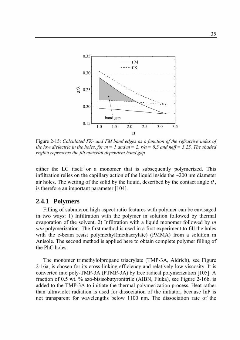
The monomer trimethylolpropane triacrylate (TMP-3A, Aldrich), see Figure
2-16a, is chosen for its cross-linking efficiency and relatively low viscosity. It is converted into poly-TMP-3A (PTMP-3A) by free radical polymerization [105]. A fraction of 0.5 wt. % azo-bisisobutyronitrile (AIBN, Fluka), see Figure 2-16b, is added to the TMP-3A to initiate the thermal polymerization process. Heat rather than ultraviolet radiation is used for dissociation of the initiator, because InP is not transparent for wavelengths below 1100 nm. The dissociation rate of the
1.0 1.5 2.0 2.5 3.0 3.50.15
0.20
0.25
0.30
0.35
band gap
ΓM ΓK
a/λ
n Figure 2-15: Calculated ΓK- and ΓM band edges as a function of the refractive index of the low dielectric in the holes, for m = 1 and m = 2, r/a = 0.3 and neff = 3.25. The shaded region represents the fill material dependent band gap.
36
AIBN must be carefully balanced, because the polymerization reaction is not properly initiated if it is too low and terminated too early if it is too high. The presence of unbounded oxygen severely inhibits the process, because it reacts efficiently with the radicals formed.
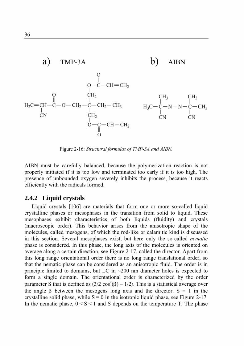
2.4.2 Liquid crystals Liquid crystals [106] are materials that form one or more so-called liquid
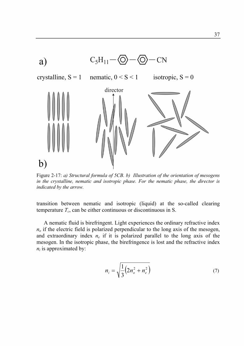
crystalline phases or mesophases in the transition from solid to liquid. These mesophases exhibit characteristics of both liquids (fluidity) and crystals (macroscopic order). This behavior arises from the anisotropic shape of the molecules, called mesogens, of which the rod-like or calamitic kind is discussed in this section. Several mesophases exist, but here only the so-called nematic phase is considered. In this phase, the long axis of the molecules is oriented on average along a certain direction, see Figure 2-17, called the director. Apart from this long range orientational order there is no long range translational order, so that the nematic phase can be considered as an anisotropic fluid. The order is in principle limited to domains, but LC in ~200 nm diameter holes is expected to form a single domain. The orientational order is characterized by the order parameter S that is defined as ⟨3/2 cos2(β) – 1/2⟩. This is a statistical average over the angle β between the mesogens long axis and the director. S = 1 in the crystalline solid phase, while S = 0 in the isotropic liquid phase, see Figure 2-17. In the nematic phase, 0 < S < 1 and S depends on the temperature T. The phase
a) TMP-3A b) AIBN
Figure 2-16: Structural formulas of TMP-3A and AIBN.
37
transition between nematic and isotropic (liquid) at the so-called clearing temperature Tc, can be either continuous or discontinuous in S.
A nematic fluid is birefringent. Light experiences the ordinary refractive index
no if the electric field is polarized perpendicular to the long axis of the mesogen, and extraordinary index ne if it is polarized parallel to the long axis of the mesogen. In the isotropic phase, the birefringence is lost and the refractive index ni is approximated by:
( )22231
eoi nnn += (7)
a)
crystalline, S = 1 nematic, 0 < S < 1 isotropic, S = 0
Figure 2-17: a) Structural formula of 5CB. b) Illustration of the orientation of mesogens in the crystalline, nematic and isotropic phase. For the nematic phase, the director is indicated by the arrow.
b)
38
The average refractive index experienced by the transmitted light depends on
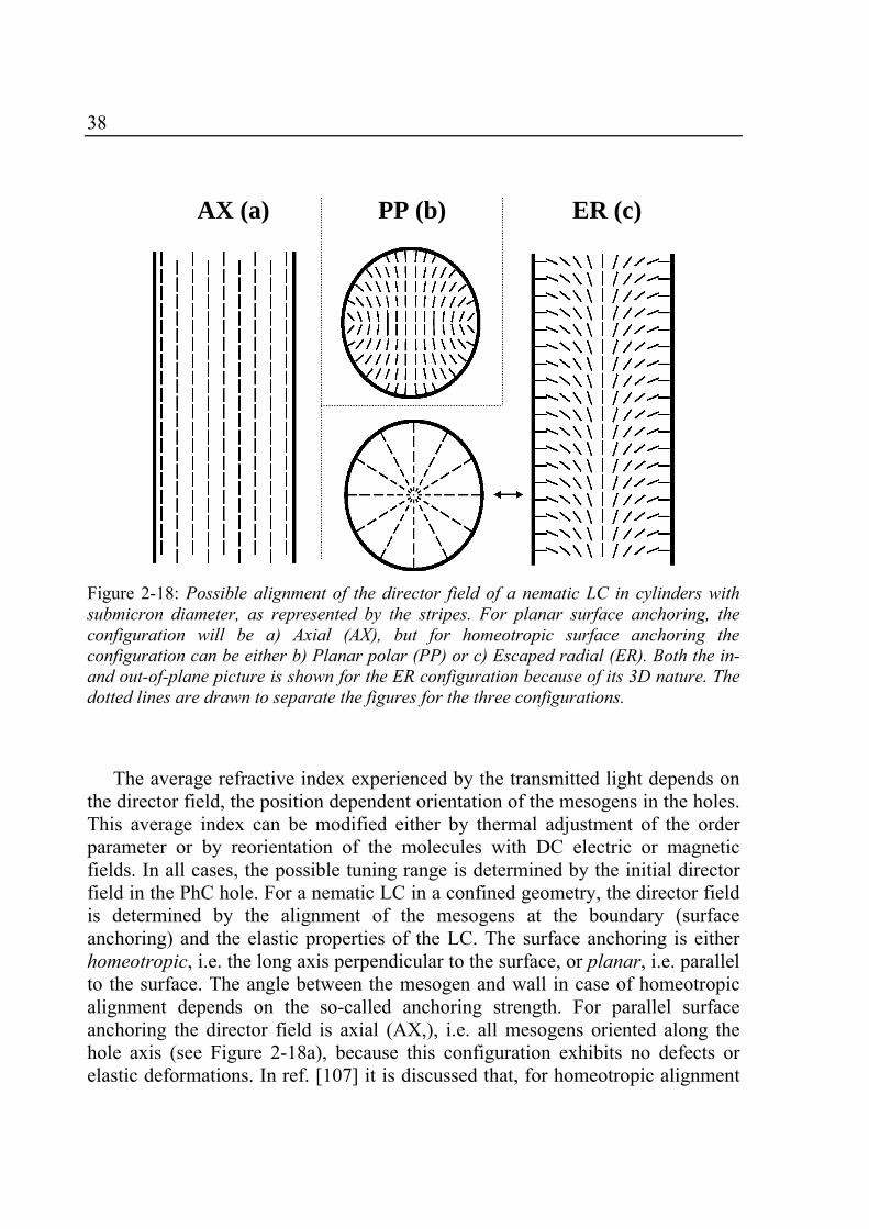
the director field, the position dependent orientation of the mesogens in the holes. This average index can be modified either by thermal adjustment of the order parameter or by reorientation of the molecules with DC electric or magnetic fields. In all cases, the possible tuning range is determined by the initial director field in the PhC hole. For a nematic LC in a confined geometry, the director field is determined by the alignment of the mesogens at the boundary (surface anchoring) and the elastic properties of the LC. The surface anchoring is either homeotropic, i.e. the long axis perpendicular to the surface, or planar, i.e. parallel to the surface. The angle between the mesogen and wall in case of homeotropic alignment depends on the so-called anchoring strength. For parallel surface anchoring the director field is axial (AX,), i.e. all mesogens oriented along the hole axis (see Figure 2-18a), because this configuration exhibits no defects or elastic deformations. In ref. [107] it is discussed that, for homeotropic alignment
AX (a) PP (b) ER (c)
Figure 2-18: Possible alignment of the director field of a nematic LC in cylinders with submicron diameter, as represented by the stripes. For planar surface anchoring, the configuration will be a) Axial (AX), but for homeotropic surface anchoring the configuration can be either b) Planar polar (PP) or c) Escaped radial (ER). Both the in- and out-of-plane picture is shown for the ER configuration because of its 3D nature. The dotted lines are drawn to separate the figures for the three configurations.
39
and r < 400 nm, the director field is either planar polar (PP), i.e. the mesogens directed in the plane according to Figure 2-18b, or escaped radial (ER, possibly with point defects), i.e. the mesogens directed in the plane at the edge of the cylinder and ‘escaping’ to the vertical direction in the centre as in Figure 2-18c.
In this work the LC 4-pentyl-4-cyanobiphenyl (5CB, also called K-15) is
infiltrated in the PPhCs. This material exhibits a crystalline-to-nematic phase transition at Tnc = 23 °C and a discontinuous nematic-to-isotropic phase transition at the T = Tc = 35 °C [108]. The refractive indices of the material at λ = 1.5 µm are no = 1.516, ne = 1.682 and ni = 1.575 [76]. It has been calculated for 5CB in cylinders with a size comparable to our PhC holes, that the director field configuration is ER in case of weak homeotropic anchoring of the mesogens at the sidewall [109].
40
Chapter 3 ICP etching results
The fabrication of low-loss PPhCs requires etching of the holes to a depth well
below the waveguide core. In fact it was discussed in section 2.1.4 that fabrication imperfections are the dominant cause for out-of-plane optical losses if the sidewall angle in the lower cladding exceeds 1°, or if the etch depth is less than 2 µm. This prompts for an etching process that is anisotropic and capable of producing holes with aspect ratio (depth divided by diameter) larger than 10. Therefore dry etching techniques as ICP etching, ECR etching and CAIBE are applied for fabrication of PPhCs. Standard parallel plate RIE is less suited, because the ion energy and plasma density cannot be controlled independently with this technique.
Good etching results for InP-based PPhCs have been achieved with CAIBE
[60, 61] and ECR [59] with Cl2-based chemistry. The use of an ion beam in CAIBE requires relatively high vacuum, which makes it difficult to operate, notably when using corrosive gases like Cl2. In ECR etching, the plasma may become unstable due to ‘mode-hopping’ [110, 111] and it has by now become replaced by ICP etching [111]. ICP etching is therefore a more reliable and versatile technique for high aspect ratio etching on a routine basis. Good results
41
on deep-hole ICP etching in InP with SiCl4-chemistry have been reported [58]. In this chapter, detailed results are presented regarding ICP etching of PPhCs
in InP-based material, using simple Cl2 gas instead of SiCl4 to provide the reactive species. It was shown in ref. [112], that sidewall passivation provides verticality of the sidewalls in pillar-type Si-based 2D PhCs. This was achieved by controlling the flux of O2 to an SF6 etching plasma. It was shown in ref. [113], that in that case the lateral etching is inhibited by the formation of an oxygen rich reaction layer on the sidewall with a thickness of less than a nanometer. On the bottom surface, this layer is removed by the ion bombardment. The selective etching of Si over its oxide then results in features with vertical sidewalls. In this thesis, the concept of sidewall passivation is extended to the etching of high aspect ratio features in InP-based material by addition of O2 or N2 to the Cl2-plasma. The Cl2/N2-chemistry was recently used in an ICP etching process for PPhCs in GaInP/GaAs material [114]. However, any role of sidewall passivation was not discussed there.
3.1 Sidewall passivation: Cl2/N2-chemistry To investigate the feasibility of sidewall passivation for InP, preliminary
experiments were performed in the MET system (see section 2.2.5) for both Cl2/Ar- and Cl2/N2 chemistry. The process parameters for the Cl2/N2 process are given in Table 3-1. For Cl2/Ar, the process parameters are the same, only Pp was set to 160 W to obtain the Vbias of 100 V. The substrate holder temperature of 220 oC is the highest possible in the system, to promote the evaporation of InCl3. These plasma parameters lead to an ion current density J = 0.7 mA/cm2 for Cl2/Ar and J = 0.5 mA/cm2 for Cl2/N2, as measured with the Langmuir probe. The plasma potential was measured to be 25 V, so that Eion = 125 eV. SEM images of ~350 nm wide trenches on a 500 nm pitch after 2 minutes of etching are shown in Figure 3-1. In the Cl2/Ar process significant lateral etching occurs as can be concluded from the undercut at the sides of the structured field in Figure 3-1a. This undercut is so large, that the ridges defined by the trenches are completely
Table 3-1: Process parameters for the etching experiments in section 3.1.
Cl2/N2 flow (sccm)
Ps (W)
Vbias (Pp) (V (W))
Tsub
(°C) p
(Pa) pHe
(mbar) 25/75 1000 -100 (300) 220 1 14
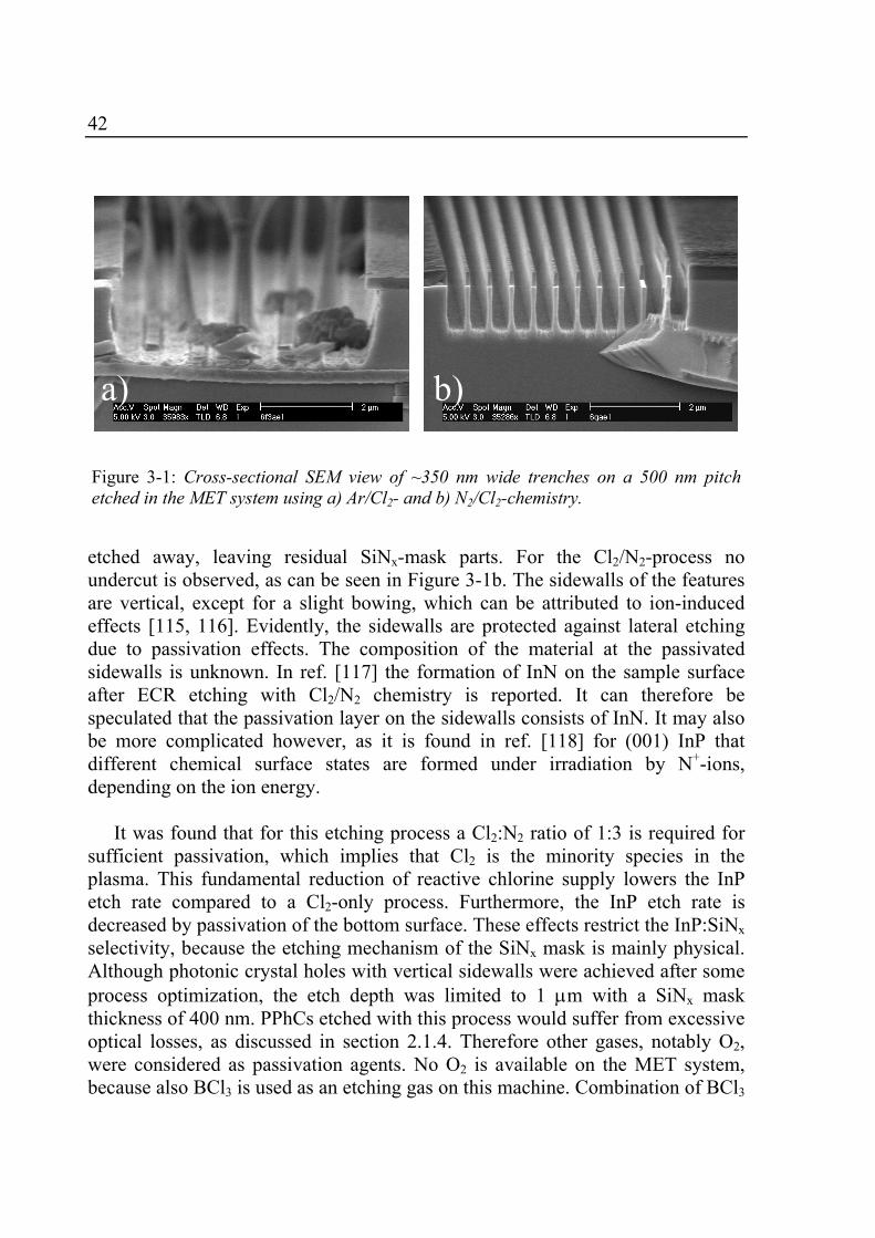
42
etched away, leaving residual SiNx-mask parts. For the Cl2/N2-process no undercut is observed, as can be seen in Figure 3-1b. The sidewalls of the features are vertical, except for a slight bowing, which can be attributed to ion-induced effects [115, 116]. Evidently, the sidewalls are protected against lateral etching due to passivation effects. The composition of the material at the passivated sidewalls is unknown. In ref. [117] the formation of InN on the sample surface after ECR etching with Cl2/N2 chemistry is reported. It can therefore be speculated that the passivation layer on the sidewalls consists of InN. It may also be more complicated however, as it is found in ref. [118] for (001) InP that different chemical surface states are formed under irradiation by N+-ions, depending on the ion energy.
It was found that for this etching process a Cl2:N2 ratio of 1:3 is required for
sufficient passivation, which implies that Cl2 is the minority species in the plasma. This fundamental reduction of reactive chlorine supply lowers the InP etch rate compared to a Cl2-only process. Furthermore, the InP etch rate is decreased by passivation of the bottom surface. These effects restrict the InP:SiNx selectivity, because the etching mechanism of the SiNx mask is mainly physical. Although photonic crystal holes with vertical sidewalls were achieved after some process optimization, the etch depth was limited to 1 µm with a SiNx mask thickness of 400 nm. PPhCs etched with this process would suffer from excessive optical losses, as discussed in section 2.1.4. Therefore other gases, notably O2, were considered as passivation agents. No O2 is available on the MET system, because also BCl3 is used as an etching gas on this machine. Combination of BCl3
Figure 3-1: Cross-sectional SEM view of ~350 nm wide trenches on a 500 nm pitch etched in the MET system using a) Ar/Cl2- and b) N2/Cl2-chemistry.
a) b)
43
and O2 can lead to formation of BO2-dust in the vacuum chamber. Therefore, experiments with Cl2/O2 were performed on the Plasmalab system (see section 2.2.5).
3.2 Cl2/O2-chemistry with moderate ICP power and high bias voltage
It was shown before, that high aspect ratio structures in Si can be obtained with fluorine (SF6) based etching using O2 for sidewall passivation [66, 112]. In refs. [119, 120] it was reported, that the native oxide can be used as mask material for free Cl2 etching of features in InP to a depth of 3 µm. This suggests that the addition of O2 to the Cl2-plasma may also be efficient in formation of a protective layer on the sidewall during InP etching. It has been shown by Smolinsky et al. that GaAs etches selectively with respect to its oxides in Cl2-plasma [121]. No selective etching of InP with respect to its oxides was observed in ref. 121. However, in their case the etching mechanism was probably rather physical as the substrate temperature (60oC) was significantly lower than required for chemical etching of InP. Cl2/O2 mixtures have been used in reactive ion etching (RIE) of InP laser stripe facets, producing vertical or even overcut sidewalls at 250 oC [122].
In this section a first investigation of Cl2/O2-chemistry for etching high aspect
ratio holes is described. The process parameters used for these experiments are given in Table 3-2. These process parameters lead to an ion current density of 0.4-0.7 mA/cm2, and a plasma potential of 60-70 V, both depending on the O2 flow. The ion energy for this process is therefore ~600 eV. No backside cooling with He was used here, to prevent the influence of He-inflow on the plasma. Therefore the thermal contact between the carrier wafer and the substrate holder is limited to the physical contact at the edge of the carrier wafer. As a result, the heating of the carrier wafer by the ion bombardment [99] causes a radial temperature gradient over the wafer in this case. The sample was positioned on
Table 3-2: Process parameters for the etching experiments of section 3.2.
Cl2/O2 flow (sccm)
Ps (W)
Vbias (Pp) (V (W))
Tsub
(°C) p
(Pa) pHe
(mbar) 7/variable 500 -530 (350) 250 0.3 0
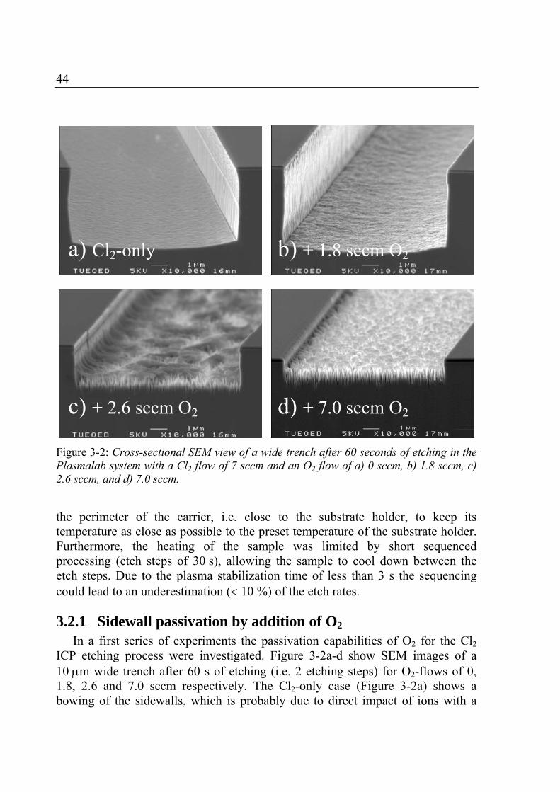
44
the perimeter of the carrier, i.e. close to the substrate holder, to keep its temperature as close as possible to the preset temperature of the substrate holder. Furthermore, the heating of the sample was limited by short sequenced processing (etch steps of 30 s), allowing the sample to cool down between the etch steps. Due to the plasma stabilization time of less than 3 s the sequencing could lead to an underestimation (< 10 %) of the etch rates.
3.2.1 Sidewall passivation by addition of O2 In a first series of experiments the passivation capabilities of O2 for the Cl2
ICP etching process were investigated. Figure 3-2a-d show SEM images of a 10 µm wide trench after 60 s of etching (i.e. 2 etching steps) for O2-flows of 0, 1.8, 2.6 and 7.0 sccm respectively. The Cl2-only case (Figure 3-2a) shows a bowing of the sidewalls, which is probably due to direct impact of ions with a
Figure 3-2: Cross-sectional SEM view of a wide trench after 60 seconds of etching in the Plasmalab system with a Cl2 flow of 7 sccm and an O2 flow of a) 0 sccm, b) 1.8 sccm, c) 2.6 sccm, and d) 7.0 sccm.
a) Cl2-only b) + 1.8 sccm O2
c) + 2.6 sccm O2 d) + 7.0 sccm O2
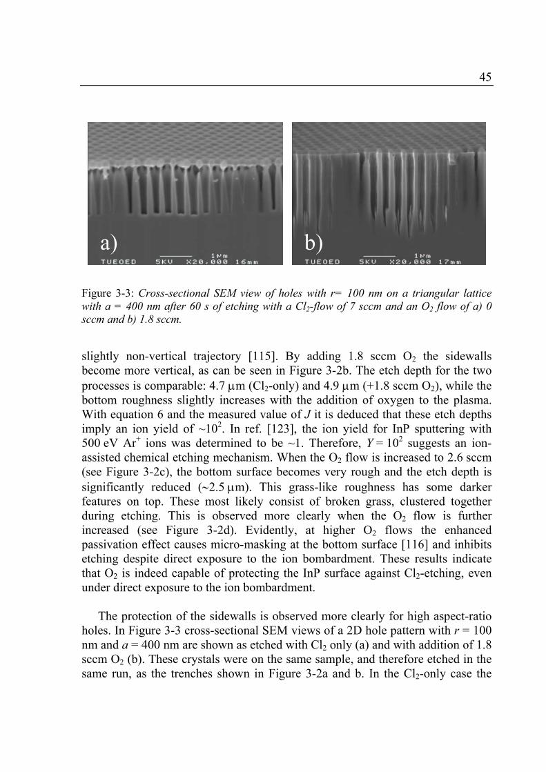
45
slightly non-vertical trajectory [115]. By adding 1.8 sccm O2 the sidewalls become more vertical, as can be seen in Figure 3-2b. The etch depth for the two processes is comparable: 4.7 µm (Cl2-only) and 4.9 µm (+1.8 sccm O2), while the bottom roughness slightly increases with the addition of oxygen to the plasma. With equation 6 and the measured value of J it is deduced that these etch depths imply an ion yield of ~102. In ref. [123], the ion yield for InP sputtering with 500 eV Ar+ ions was determined to be ~1. Therefore, Y = 102 suggests an ion-assisted chemical etching mechanism. When the O2 flow is increased to 2.6 sccm (see Figure 3-2c), the bottom surface becomes very rough and the etch depth is significantly reduced (∼2.5 µm). This grass-like roughness has some darker features on top. These most likely consist of broken grass, clustered together during etching. This is observed more clearly when the O2 flow is further increased (see Figure 3-2d). Evidently, at higher O2 flows the enhanced passivation effect causes micro-masking at the bottom surface [116] and inhibits etching despite direct exposure to the ion bombardment. These results indicate that O2 is indeed capable of protecting the InP surface against Cl2-etching, even under direct exposure to the ion bombardment.
The protection of the sidewalls is observed more clearly for high aspect-ratio
holes. In Figure 3-3 cross-sectional SEM views of a 2D hole pattern with r = 100 nm and a = 400 nm are shown as etched with Cl2 only (a) and with addition of 1.8 sccm O2 (b). These crystals were on the same sample, and therefore etched in the same run, as the trenches shown in Figure 3-2a and b. In the Cl2-only case the
Figure 3-3: Cross-sectional SEM view of holes with r= 100 nm on a triangular lattice with a = 400 nm after 60 s of etching with a Cl2-flow of 7 sccm and an O2 flow of a) 0 sccm and b) 1.8 sccm.
a) b)
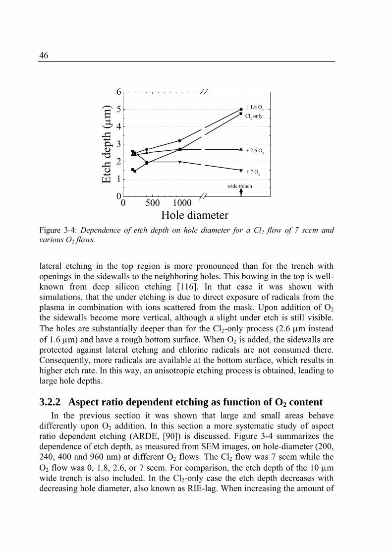
46
lateral etching in the top region is more pronounced than for the trench with openings in the sidewalls to the neighboring holes. This bowing in the top is well-known from deep silicon etching [116]. In that case it was shown with simulations, that the under etching is due to direct exposure of radicals from the plasma in combination with ions scattered from the mask. Upon addition of O2 the sidewalls become more vertical, although a slight under etch is still visible. The holes are substantially deeper than for the Cl2-only process (2.6 µm instead of 1.6 µm) and have a rough bottom surface. When O2 is added, the sidewalls are protected against lateral etching and chlorine radicals are not consumed there. Consequently, more radicals are available at the bottom surface, which results in higher etch rate. In this way, an anisotropic etching process is obtained, leading to large hole depths.
3.2.2 Aspect ratio dependent etching as function of O2 content In the previous section it was shown that large and small areas behave
differently upon O2 addition. In this section a more systematic study of aspect ratio dependent etching (ARDE, [90]) is discussed. Figure 3-4 summarizes the dependence of etch depth, as measured from SEM images, on hole-diameter (200, 240, 400 and 960 nm) at different O2 flows. The Cl2 flow was 7 sccm while the O2 flow was 0, 1.8, 2.6, or 7 sccm. For comparison, the etch depth of the 10 µm wide trench is also included. In the Cl2-only case the etch depth decreases with decreasing hole diameter, also known as RIE-lag. When increasing the amount of
0 500 1000 1500 2000 2500
1
2
3
4
5
6
wide trench
+ 7 O2
+ 2.6 O2
Cl2 onlyEt
ch d
epth
(µm
)
Hole diameter
+ 1.8 O2
Figure 3-4: Dependence of etch depth on hole diameter for a Cl2 flow of 7 sccm and various O2 flows.
47
O2 the RIE-lag is reduced, eventually leading to inverse RIE-lag (etch depth increase with decreasing hole diameter) at the largest O2 flow. The consequences of O2 addition for the overall etch behavior with respect to ARDE are twofold, each with a different impact. On one hand improved sidewall passivation leads to enhanced exposure of the bottom to reactive species, which will increase the etch rate. On the other hand improved bottom passivation leads inevitably to lower etch rates.
The results in Figure 3-4 indicate that the resultant of the two effects varies
largely with aspect ratio (AR). In the lower AR regime (960 nm diameter hole, 10 µm trench) the enhanced bottom passivation and slow down of the etch rate dominates for increasing O2 content after a slight increase at the lowest O2 addition (1.8 sccm). In the high aspect ratio regime (200 and 240 nm diameter) the impact of sidewall passivation and the correspondingly enhanced flux of reactive species to the bottom dominates. The hole depth is independent of the O2 flow in the range investigated. The same etch behavior is also observed using a higher Cl2-flow of 14 sccm, but then the hole depth is significantly larger. This suggests that, in this etching regime, the ion-enhanced etching is limited by the supply of neutral Cl species. The abundance of neutrals at the bottom surface is strongly dependent on the aspect ratio of the hole [115]. Apparently, in this pressure- and flow regime, insufficient O2 is available to passivate the bottom surface of the holes under the ion bombardment.
It is pointed out that with a proper Cl2/O2 balance the etching process can be
tuned to aspect ratio independent etching, as manifested by the 2.6 sccm O2 curve in Figure 3-4. This may be very useful when structures with various feature sizes are to be realized in a single etch step. Apart from all surface chemical effects at sidewall and bottom, the addition of oxygen increases the dissociation of chlorine since the strong electron attachment mechanism for chlorine is suppressed [124]. The systematic increase of the etch depth when 1.8 sccm of O2 is added could be partly ascribed to this effect.
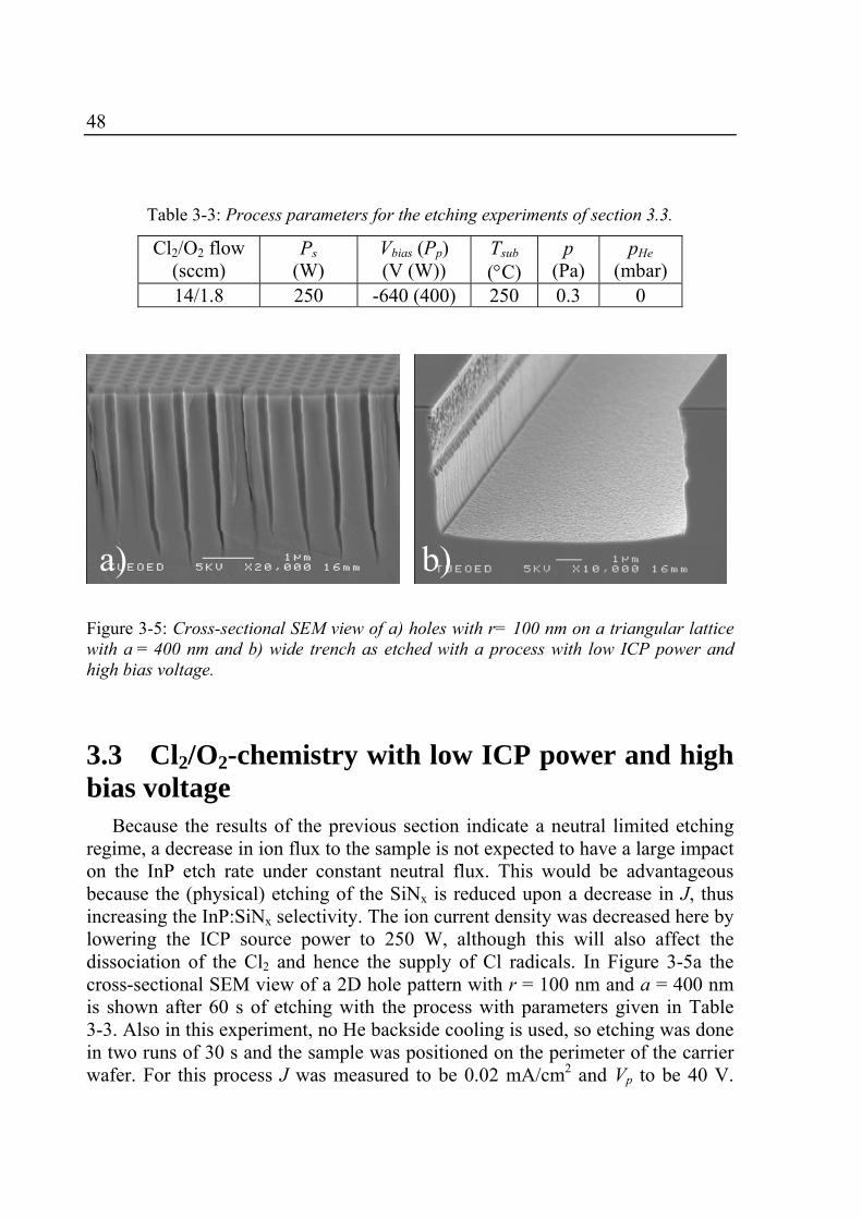
48
3.3 Cl2/O2-chemistry with low ICP power and high bias voltage
Because the results of the previous section indicate a neutral limited etching regime, a decrease in ion flux to the sample is not expected to have a large impact on the InP etch rate under constant neutral flux. This would be advantageous because the (physical) etching of the SiNx is reduced upon a decrease in J, thus increasing the InP:SiNx selectivity. The ion current density was decreased here by lowering the ICP source power to 250 W, although this will also affect the dissociation of the Cl2 and hence the supply of Cl radicals. In Figure 3-5a the cross-sectional SEM view of a 2D hole pattern with r = 100 nm and a = 400 nm is shown after 60 s of etching with the process with parameters given in Table 3-3. Also in this experiment, no He backside cooling is used, so etching was done in two runs of 30 s and the sample was positioned on the perimeter of the carrier wafer. For this process J was measured to be 0.02 mA/cm2 and Vp to be 40 V.
Table 3-3: Process parameters for the etching experiments of section 3.3.
Cl2/O2 flow (sccm)
Ps (W)
Vbias (Pp) (V (W))
Tsub
(°C) p
(Pa) pHe
(mbar) 14/1.8 250 -640 (400) 250 0.3 0
Figure 3-5: Cross-sectional SEM view of a) holes with r= 100 nm on a triangular lattice with a = 400 nm and b) wide trench as etched with a process with low ICP power and high bias voltage.
a) b)
49
Therefore Eion = 680 eV. The holes in Figure 3-5a are deep (∼3.4 µm) with almost vertical (< 1°)
sidewalls in the upper 2 µm. It is therefore expected, that this etching process yields low-loss PPhCs, see section 2.1.4. The bottom part of the high aspect ratio holes is narrow, which appears to be a commonly encountered feature in PPhC etching in InP [59, 60, 61], and may relate to ion shadowing effects [90]. It is visible in Figure 3-5a, that a substantial part of the mask is still present after etching (200 nm). The InP:SiNx selectivity for large area etching is 20 for this process, similar to the process described in the previous section (but with Cl2 flow of 14 instead of 7 sccm). This is probably due to the higher ion energy here. The residual SiNx visible in Figure 3-5a has a thickness of 140 nm, which would allow another ~30 s of etching.
For the trench, depicted in Figure 3-5b, the whole upper region of the sidewall
is very rough and there is a marked transition to the smoother lower region. Similar abrupt transitions in sidewall roughness have been observed before with other dry etching processes, including Cl2/O2-RIE and were attributed to redeposition of non-volatile etch products [122, 125]. This transition is also observed in the Cl2 only case, though less pronounced (Figure 3-2a). The trench profile would lead to important propagation losses in the ridge waveguide, which makes this process less suitable when both ridge waveguides and PhCs have to be etched in a single process step.
3.4 Cl2/O2-chemistry with high ICP power and low bias voltage: influence of sample temperature
In the previous sections, no He backflow for thermal contact between the substrate holder and carrier wafer was used. It was shown by Sabin however, that the ion bombardment may lead to significant heating of the sample, with a temperature increase up to 75 °C [99]. The InP etch rate by Cl2 gas shows an activated dependence on the temperature [95], so it is expected that accurate control of the sample temperature is important. In the following, the influence of the He backside cooling and the temperature dependence of the etching are discussed. The process parameters for these experiments are given in Table 3-4. Although no Langmuir probe measurements were performed for this particular process, the values for J and Vp were estimated from values for other processes to be ~1 mA/cm2 and ~40 V respectively, the latter leading to Eion ≈ 270 eV. Etching
50
was performed here in a single step, i.e. without the 30 s sequencing of the previous experiments.
3.4.1 He backside cooling The importance of the He backside cooling is illustrated in Figure 3-6. The
SEM views in this figure are trenches after 60 s of etching and result from four samples in two different etching experiments. In each experiment one sample was positioned at the perimeter of the carrier wafer (right of Figure 3-6), as in the experiments described in the previous sections, and the other in the centre of the carrier wafer (left of Figure 3-6). One of the experiments was performed without He backside cooling (top of Figure 3-6) and the other with cooling (11 sccm He flow into the reactor, bottom of Figure 3-6). For both, the temperature of the substrate holder was set to 250 °C. The difference in etching result with (Figure 3-6a and b) and without (Figure 3-6c and d) cooling is striking. For the samples etched with He backside cooling, the trenches exhibit a grass type surface roughness, while no grass is present for the trenches etched without cooling. In a separate experiment with the sample positioned in the centre of the carrier wafer, the same He backside pressure (24 mbar) and a preset temperature of 300 °C, the bottom surface is similar to the sample etched without cooling in the centre of the carrier wafer (Figure 3-6a). The high temperature may cause an enhanced lateral etching of the grass pillars. It can be concluded, that the He backside cooling partly prevents heating by the ion bombardment, leading to a sample temperature that may be ~50 °C lower than without cooling. This reduces the dependence of the sample temperature on fluctuations in J and/or Eion and therefore improves the reproducibility of the etching.
Table 3-4: Process parameters for the etching experiments of section 3.4.
Cl2/O2 flow (sccm)
Ps (W)
Vbias (Pp) (V (W))
Tsub
(°C) p
(Pa) pHe
(mbar) 14/3.8 1000 -230 (160) variable 0.3 24
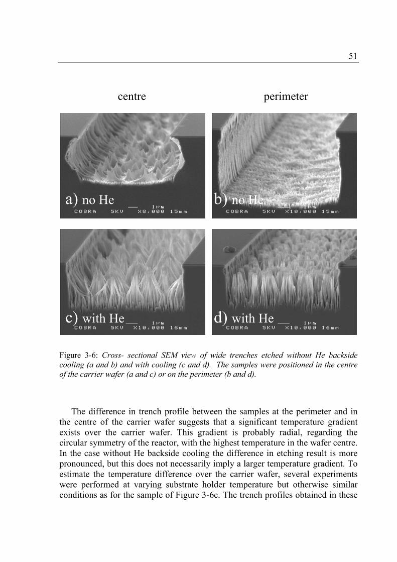
51
The difference in trench profile between the samples at the perimeter and in
the centre of the carrier wafer suggests that a significant temperature gradient exists over the carrier wafer. This gradient is probably radial, regarding the circular symmetry of the reactor, with the highest temperature in the wafer centre. In the case without He backside cooling the difference in etching result is more pronounced, but this does not necessarily imply a larger temperature gradient. To estimate the temperature difference over the carrier wafer, several experiments were performed at varying substrate holder temperature but otherwise similar conditions as for the sample of Figure 3-6c. The trench profiles obtained in these
centre perimeter
Figure 3-6: Cross- sectional SEM view of wide trenches etched without He backside cooling (a and b) and with cooling (c and d). The samples were positioned in the centre of the carrier wafer (a and c) or on the perimeter (b and d).
a) no He b) no He
c) with He d) with He
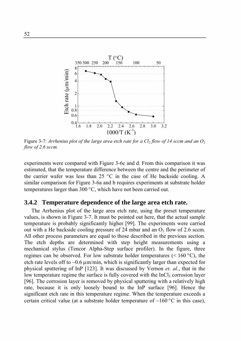
52
experiments were compared with Figure 3-6c and d. From this comparison it was estimated, that the temperature difference between the centre and the perimeter of the carrier wafer was less than 25 °C in the case of He backside cooling. A similar comparison for Figure 3-6a and b requires experiments at substrate holder temperatures larger than 300 °C, which have not been carried out.
3.4.2 Temperature dependence of the large area etch rate. The Arrhenius plot of the large area etch rate, using the preset temperature
values, is shown in Figure 3-7. It must be pointed out here, that the actual sample temperature is probably significantly higher [99]. The experiments were carried out with a He backside cooling pressure of 24 mbar and an O2 flow of 2.6 sccm. All other process parameters are equal to those described in the previous section. The etch depths are determined with step height measurements using a mechanical stylus (Tencor Alpha-Step surface profiler). In the figure, three regimes can be observed. For low substrate holder temperatures (< 160 °C), the etch rate levels off to ~0.6 µm/min, which is significantly larger than expected for physical sputtering of InP [123]. It was discussed by Vernon et. al., that in the low temperature regime the surface is fully covered with the InCl3 corrosion layer [96]. The corrosion layer is removed by physical sputtering with a relatively high rate, because it is only loosely bound to the InP surface [96]. Hence the significant etch rate in this temperature regime. When the temperature exceeds a certain critical value (at a substrate holder temperature of ~160 °C in this case),
1.6 1.8 2.0 2.2 2.4 2.6 2.8 3.0 3.20.4
0.60.8
1
2
4
68350 300 250 200 150 100 50
T (°C)Et
ch ra
te (µ
m/m
in)
1000/T (K-1) Figure 3-7: Arrhenius plot of the large area etch rate for a Cl2 flow of 14 sccm and an O2 flow of 2.6 sccm.
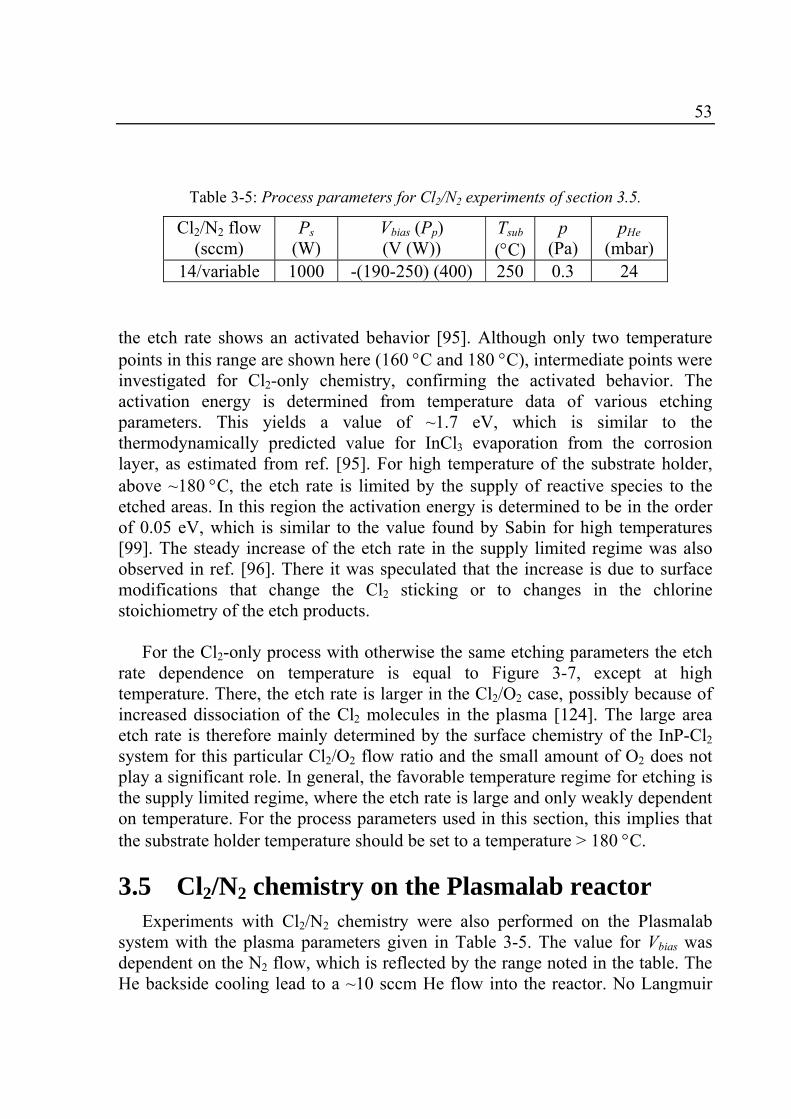
53
the etch rate shows an activated behavior [95]. Although only two temperature points in this range are shown here (160 °C and 180 °C), intermediate points were investigated for Cl2-only chemistry, confirming the activated behavior. The activation energy is determined from temperature data of various etching parameters. This yields a value of ~1.7 eV, which is similar to the thermodynamically predicted value for InCl3 evaporation from the corrosion layer, as estimated from ref. [95]. For high temperature of the substrate holder, above ~180 °C, the etch rate is limited by the supply of reactive species to the etched areas. In this region the activation energy is determined to be in the order of 0.05 eV, which is similar to the value found by Sabin for high temperatures [99]. The steady increase of the etch rate in the supply limited regime was also observed in ref. [96]. There it was speculated that the increase is due to surface modifications that change the Cl2 sticking or to changes in the chlorine stoichiometry of the etch products.
For the Cl2-only process with otherwise the same etching parameters the etch
rate dependence on temperature is equal to Figure 3-7, except at high temperature. There, the etch rate is larger in the Cl2/O2 case, possibly because of increased dissociation of the Cl2 molecules in the plasma [124]. The large area etch rate is therefore mainly determined by the surface chemistry of the InP-Cl2 system for this particular Cl2/O2 flow ratio and the small amount of O2 does not play a significant role. In general, the favorable temperature regime for etching is the supply limited regime, where the etch rate is large and only weakly dependent on temperature. For the process parameters used in this section, this implies that the substrate holder temperature should be set to a temperature > 180 °C.
3.5 Cl2/N2 chemistry on the Plasmalab reactor Experiments with Cl2/N2 chemistry were also performed on the Plasmalab
system with the plasma parameters given in Table 3-5. The value for Vbias was dependent on the N2 flow, which is reflected by the range noted in the table. The He backside cooling lead to a ~10 sccm He flow into the reactor. No Langmuir
Table 3-5: Process parameters for Cl2/N2 experiments of section 3.5.
Cl2/N2 flow (sccm)
Ps (W)
Vbias (Pp) (V (W))
Tsub
(°C)p
(Pa) pHe
(mbar) 14/variable 1000 -(190-250) (400) 250 0.3 24
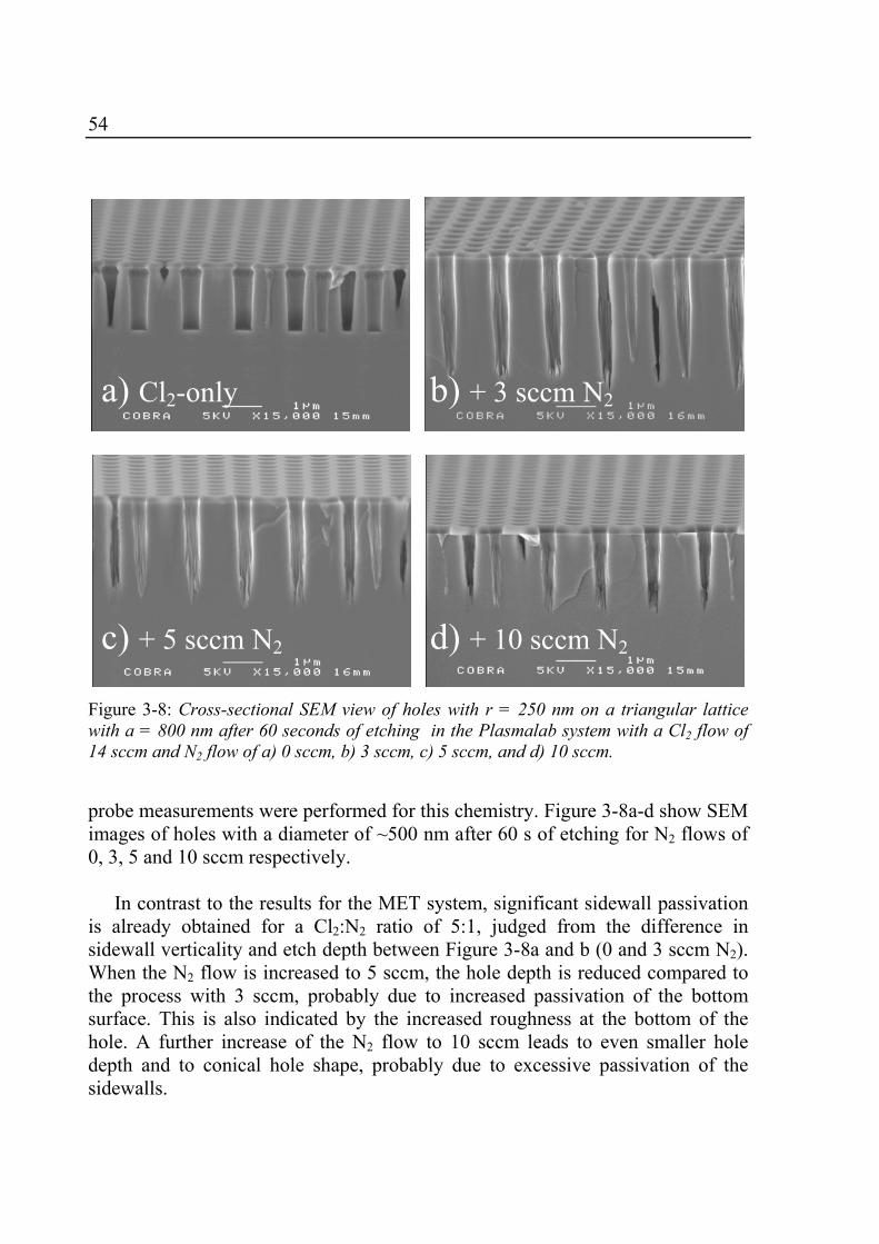
54
probe measurements were performed for this chemistry. Figure 3-8a-d show SEM images of holes with a diameter of ~500 nm after 60 s of etching for N2 flows of 0, 3, 5 and 10 sccm respectively.
In contrast to the results for the MET system, significant sidewall passivation
is already obtained for a Cl2:N2 ratio of 5:1, judged from the difference in sidewall verticality and etch depth between Figure 3-8a and b (0 and 3 sccm N2). When the N2 flow is increased to 5 sccm, the hole depth is reduced compared to the process with 3 sccm, probably due to increased passivation of the bottom surface. This is also indicated by the increased roughness at the bottom of the hole. A further increase of the N2 flow to 10 sccm leads to even smaller hole depth and to conical hole shape, probably due to excessive passivation of the sidewalls.
Figure 3-8: Cross-sectional SEM view of holes with r = 250 nm on a triangular lattice with a = 800 nm after 60 seconds of etching in the Plasmalab system with a Cl2 flow of 14 sccm and N2 flow of a) 0 sccm, b) 3 sccm, c) 5 sccm, and d) 10 sccm.
a) Cl2-only b) + 3 sccm N2
c) + 5 sccm N2 d) + 10 sccm N2
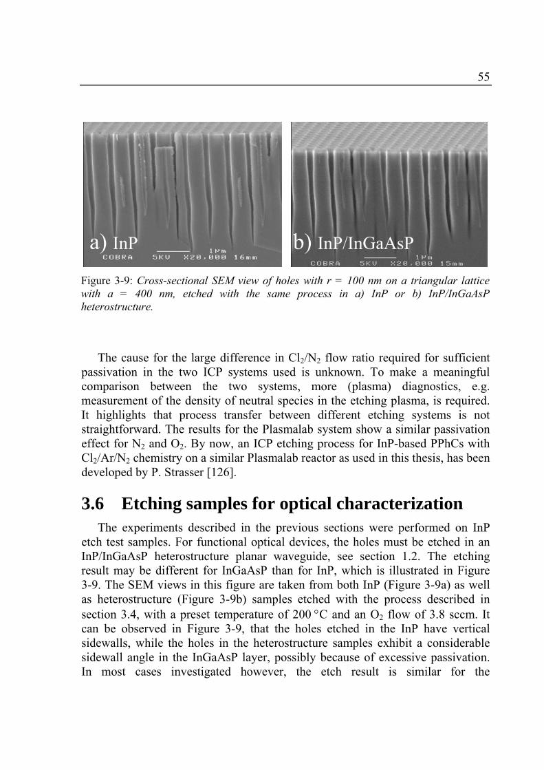
55
The cause for the large difference in Cl2/N2 flow ratio required for sufficient
passivation in the two ICP systems used is unknown. To make a meaningful comparison between the two systems, more (plasma) diagnostics, e.g. measurement of the density of neutral species in the etching plasma, is required. It highlights that process transfer between different etching systems is not straightforward. The results for the Plasmalab system show a similar passivation effect for N2 and O2. By now, an ICP etching process for InP-based PPhCs with Cl2/Ar/N2 chemistry on a similar Plasmalab reactor as used in this thesis, has been developed by P. Strasser [126].
3.6 Etching samples for optical characterization The experiments described in the previous sections were performed on InP
etch test samples. For functional optical devices, the holes must be etched in an InP/InGaAsP heterostructure planar waveguide, see section 1.2. The etching result may be different for InGaAsP than for InP, which is illustrated in Figure 3-9. The SEM views in this figure are taken from both InP (Figure 3-9a) as well as heterostructure (Figure 3-9b) samples etched with the process described in section 3.4, with a preset temperature of 200 °C and an O2 flow of 3.8 sccm. It can be observed in Figure 3-9, that the holes etched in the InP have vertical sidewalls, while the holes in the heterostructure samples exhibit a considerable sidewall angle in the InGaAsP layer, possibly because of excessive passivation. In most cases investigated however, the etch result is similar for the
Figure 3-9: Cross-sectional SEM view of holes with r = 100 nm on a triangular lattice with a = 400 nm, etched with the same process in a) InP or b) InP/InGaAsP heterostructure.
a) InP b) InP/InGaAsP
56
heterostructure and plain InP. If not so, a small adjustment of the process parameters is sufficient to correct for the different etching behavior. In the example of Figure 3-9, vertical sidewalls are obtained for the heterostructure sample by lowering the O2 flow to 2.6 sccm. This confirms the approach of process development using InP substrates and subsequent fine tuning of the process with (more expensive) heterostructure material.
For optical characterization, ridge waveguides and PPhC areas are
monolithically integrated and etched in a single process step. Therefore, the ICP process of choice is a compromise between the quality of the holes and that of the ridge. The sidewall passivation concept developed and described in this chapter
Cl2-only Cl2/O2
Figure 3-10: Cross-sectional SEM view of holes with r = 100 nm on a triangular lattice with a = 400 nm, etched with a Cl2 flow of 14 sccm and a) no O2 at 180 °C, b) 3.0 sccm O2 at 200 °C, c) no O2 at 250 °C, and d) 3.8 sccm O2 at 250 °C.
a) 180 °C b) 200 °C
c) 250 °C d) 250 °C
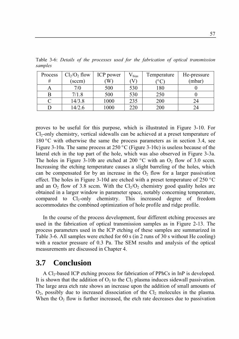
57
proves to be useful for this purpose, which is illustrated in Figure 3-10. For Cl2-only chemistry, vertical sidewalls can be achieved at a preset temperature of 180 °C with otherwise the same the process parameters as in section 3.4, see Figure 3-10a. The same process at 250 °C (Figure 3-10c) is useless because of the lateral etch in the top part of the hole, which was also observed in Figure 3-3a. The holes in Figure 3-10b are etched at 200 °C with an O2 flow of 3.0 sccm. Increasing the etching temperature causes a slight barreling of the holes, which can be compensated for by an increase in the O2 flow for a larger passivation effect. The holes in Figure 3-10d are etched with a preset temperature of 250 °C and an O2 flow of 3.8 sccm. With the Cl2/O2 chemistry good quality holes are obtained in a larger window in parameter space, notably concerning temperature, compared to Cl2-only chemistry. This increased degree of freedom accommodates the combined optimization of hole profile and ridge profile.
In the course of the process development, four different etching processes are
used in the fabrication of optical transmission samples as in Figure 2-13. The process parameters used in the ICP etching of these samples are summarized in Table 3-6. All samples were etched for 60 s (in 2 runs of 30 s without He cooling) with a reactor pressure of 0.3 Pa. The SEM results and analysis of the optical measurements are discussed in Chapter 4.
3.7 Conclusion A Cl2-based ICP etching process for fabrication of PPhCs in InP is developed.
It is shown that the addition of O2 to the Cl2 plasma induces sidewall passivation. The large area etch rate shows an increase upon the addition of small amounts of O2, possibly due to increased dissociation of the Cl2 molecules in the plasma. When the O2 flow is further increased, the etch rate decreases due to passivation
Table 3-6: Details of the processes used for the fabrication of optical transmission samples
Process #
Cl2/O2 flow (sccm)
ICP power (W)
Vbias (V)
Temperature (°C)
He-pressure (mbar)
A 7/0 500 530 180 0 B 7/1.8 500 530 250 0 C 14/3.8 1000 235 200 24 D 14/2.6 1000 220 200 24
58
of the surface. The depth of holes with r = 100 nm is independent of O2 flow in the flow regime investigated. Therefore, the etch depth is independent of aspect ratio for a specific Cl2/O2-ratio.
The temperature dependence of the large area etch rate reveals three etching
regimes in the temperature range investigated. For a substrate holder temperature (which is not equal to the temperature of the sample) below 160 °C, the etch rate levels off at 0.6 µm. In this regime the etching is most likely due to physical sputtering of an InCl3 corrosion layer that fully covers the InP surface. Above 160 °C, the InCl3 is enough volatile to evaporate from the surface and the etching proceeds with an activated dependence on temperature. For a substrate temperature larger than 180 °C, the etch rate is limited by the supply of reactive species to the etched areas. It is shown that He backside cooling reduces the heating of the carrier wafer induced by the ion bombardment, which allows for better control of the sample temperature.
Etching experiments with Cl2/N2 chemistry are performed in two different
reactors. Sidewall passivation can be achieved with N2 in both reactors, but at very different Cl2/N2 ratio. The reason for this is yet unknown. However it is shown for the Plasmalab reactor, that O2 and N2 have a similar passivation effect.
Holes with good quality (i.e. sufficiently deep and cylindrical) are obtained for
both a process with low ICP power (250 W) and high bias voltage (-640 V) and a process with high ICP power (1000 W) and relatively low bias voltage (-230 V). The processes developed for InP material may require some fine tuning for heterostructure samples, although in many cases the etching profiles are similar. It is shown that with Cl2/O2 chemistry, holes with good quality are obtained within a larger window in parameter space, notably concerning temperature, compared to Cl2-only chemistry. The application of the sidewall passivation concept to InP material thus accommodates the combined optimization of hole profile and ridge profile in etching of optical transmission samples.

59
60
Chapter 4 Optical characterization
Various methods are used to experimentally asses the optical properties of PPhCs. Frequently, the in plane optical transmission of PPhC structures, which can include (a combination of) defects, is measured for this purpose. This requires an incoming guided wave on one side- and collection of the transmission on the other side of the PhC. The incoming light arises either from excited nanostructures inside the waveguide core (ILS method, see section 1.3.2) or from an external source (end-fire method, see section 1.3.2). In the latter case, incoupling of the light in the waveguide core layer is mostly done by focusing at end facets, but also prism coupling [127] or integrated grating couplers [128] are used.
In the transmission measurements, additional information can be obtained by
imaging the light scattered upwards (out-of-plane) by the PPhC in the far field, see for instance [129]. A fundamentally different method is so-called near-field scanning optical microscopy (NSOM) or, equivalently, photon scanning tunneling microscopy, which is often used in combination with a transmission set-up. For a recent review on NSOM, see ref. [130]. The guided PhC modes are detected by coupling the evanescent field into a propagating wave inside an optical fiber probe, which has a subwavelength aperture (25-100 nm). The probe
61
is raster scanned over the sample surface, while keeping the distance to the surface constant at 5-50 nm, to obtain topological information as well. With NSOM the characteristics of PhC modes can be assessed with a spatial resolution << λ. With a heterodyne interferometric approach, this can even be done dynamically [131]. The latter has been performed for instance for fs-pulses [132] and low group velocity modes [49] in PhC line defects.
It is possible to obtain information on the band structure of a PPhC from
transmission measurements. This is done by analysis of the fine structure in the transmission bands that arises from interference of the Bloch modes between the PhC boundaries [101]. Alternatively, band structure information can be obtained from the angle dependent out-of-plane reflection spectrum [133]. The incoming light is coupled to a PPhC mode if the parallel components of the wave vectors match. For a specific input angle of the probe light with the sample surface this leads to resonances in the reflection spectrum at specific wavelengths. From these, the (ω, k)-pairs for the specific PhC modes can be deduced and the full band structure is obtained by scanning the input angle. This method only resolves the bands above the light line, as the ones below the light line cannot couple to free space modes.
Optical end-fire transmission measurements for PPhCs were first performed
by Krauss et. al. with a configuration similar to Figure 2-1, based on (Al)GaAs material [15]. They observed clear signatures of the photonic stop gaps with > 2 decades optical extinction in the gaps. This was reproduced by Chow et. al., who showed evidence of polarization conversion in the PhC due to the asymmetry of the vertical waveguide structure [103]. As the waveguide structure used for the PPhC in this thesis is symmetric, it induces no polarization conversion.
In the remainder of this chapter, the end-fire transmission measurements
performed are discussed in detail. The results are analyzed in the framework of the loss parameter model as discussed in sections 2.1.3 and 2.1.4, to assess the quality of the etched holes. This approach combines the advantages of the end-fire method (see section 1.3.2) with the versatility of the loss parameter model. In the course of the process development, several PPhCs with large differences in hole quality are produced. Four of these processes are evaluated here, and an unprecedented loss parameter range is observed.
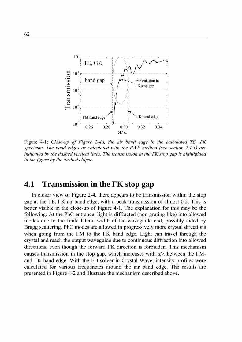
62
4.1 Transmission in the ΓK stop gap In closer view of Figure 2-4, there appears to be transmission within the stop
gap at the TE, ΓK air band edge, with a peak transmission of almost 0.2. This is better visible in the close-up of Figure 4-1. The explanation for this may be the following. At the PhC entrance, light is diffracted (non-grating like) into allowed modes due to the finite lateral width of the waveguide end, possibly aided by Bragg scattering. PhC modes are allowed in progressively more crystal directions when going from the ΓM to the ΓK band edge. Light can travel through the crystal and reach the output waveguide due to continuous diffraction into allowed directions, even though the forward ΓK direction is forbidden. This mechanism causes transmission in the stop gap, which increases with a/λ between the ΓM- and ΓK band edge. With the FD solver in Crystal Wave, intensity profiles were calculated for various frequencies around the air band edge. The results are presented in Figure 4-2 and illustrate the mechanism described above.
0.26 0.28 0.30 0.32 0.3410-4
10-3
10-2
10-1
100
transmission inΓK stop gap
ΓM band edge ΓK band edge
TE, GK T
rans
mis
sion
a/λ
band gap
Figure 4-1: Close-up of Figure 2-4a, the air band edge in the calculated TE, ΓK spectrum. The band edges as calculated with the PWE method (see section 2.1.1) are indicated by the dashed vertical lines. The transmission in the ΓK stop gap is highlighted in the figure by the dashed ellipse.
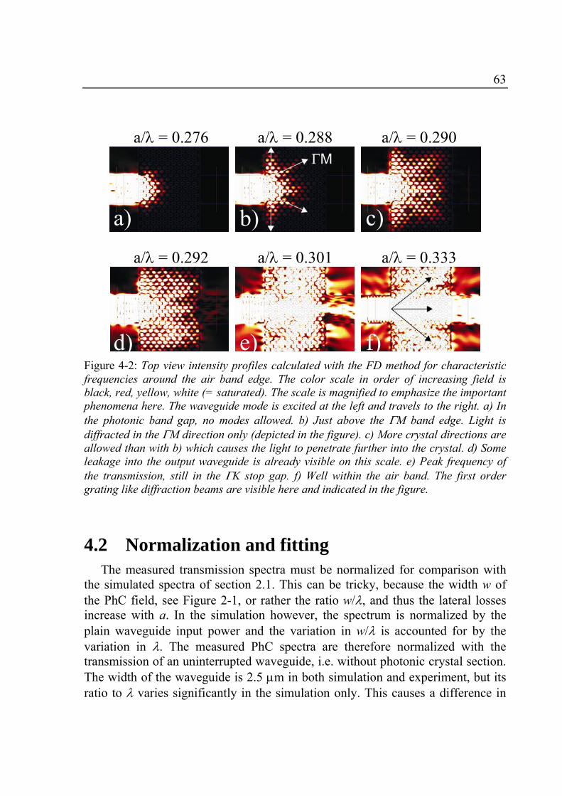
63
4.2 Normalization and fitting The measured transmission spectra must be normalized for comparison with
the simulated spectra of section 2.1. This can be tricky, because the width w of the PhC field, see Figure 2-1, or rather the ratio w/λ, and thus the lateral losses increase with a. In the simulation however, the spectrum is normalized by the plain waveguide input power and the variation in w/λ is accounted for by the variation in λ. The measured PhC spectra are therefore normalized with the transmission of an uninterrupted waveguide, i.e. without photonic crystal section. The width of the waveguide is 2.5 µm in both simulation and experiment, but its ratio to λ varies significantly in the simulation only. This causes a difference in
a/λ = 0.276 a/λ = 0.288 a/λ = 0.290
a/λ = 0.292 a/λ = 0.301 a/λ = 0.333
Figure 4-2: Top view intensity profiles calculated with the FD method for characteristic frequencies around the air band edge. The color scale in order of increasing field is black, red, yellow, white (= saturated). The scale is magnified to emphasize the important phenomena here. The waveguide mode is excited at the left and travels to the right. a) In the photonic band gap, no modes allowed. b) Just above the ΓM band edge. Light is diffracted in the ΓM direction only (depicted in the figure). c) More crystal directions are allowed than with b) which causes the light to penetrate further into the crystal. d) Some leakage into the output waveguide is already visible on this scale. e) Peak frequency of the transmission, still in the ΓK stop gap. f) Well within the air band. The first order grating like diffraction beams are visible here and indicated in the figure.
a)
f) e) d)
b) c)
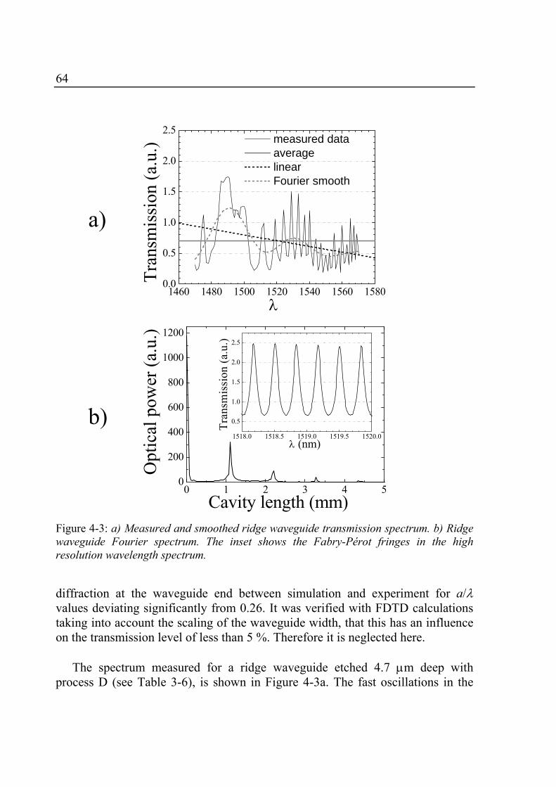
64
diffraction at the waveguide end between simulation and experiment for a/λ values deviating significantly from 0.26. It was verified with FDTD calculations taking into account the scaling of the waveguide width, that this has an influence on the transmission level of less than 5 %. Therefore it is neglected here.
The spectrum measured for a ridge waveguide etched 4.7 µm deep with
process D (see Table 3-6), is shown in Figure 4-3a. The fast oscillations in the
1460 1480 1500 1520 1540 1560 15800.0
0.5
1.0
1.5
2.0
2.5 measured data average linear Fourier smooth
Tran
smis
sion
(a.u
.)
λ
0 1 2 3 4 50
200
400
600
800
1000
1200
1518.0 1518.5 1519.0 1519.5 1520.0
0.5
1.0
1.5
2.0
2.5
Tran
smis
sion
(a.u
.)
λ (nm)
Opt
ical
pow
er (a
.u.)
Cavity length (mm) Figure 4-3: a) Measured and smoothed ridge waveguide transmission spectrum. b) Ridge waveguide Fourier spectrum. The inset shows the Fabry-Pérot fringes in the high resolution wavelength spectrum.
a)
b)
65
spectrum are of Fabry-Pérot type due to reflections between the end facets, cavity 6 in Figure 2-13. The Fourier transform of a spectral region limited to 5 nm to obtain sharp peaks is shown in Figure 4-3b. The corresponding wavelength spectrum was measured with 0.01 nm steps to resolve the higher harmonic peaks, and is shown in the inset of Figure 4-3b. The first Fourier peak appears at a cavity length of 1.1 mm, which is equal to the sample width. This peak therefore indeed represents the cavity that is formed by the end facets. The subsequent peaks are the higher harmonics at integer multiples of 1.1 mm. The waveguide propagation loss is calculated from the wavelength spectrum using the ratio of maximum and minimum transmission of the fringes (equation 5 in ref. [134]. The dielectric-air facet reflectance was calculated1 to be 0.33. A propagation loss of 2 dB/cm is deduced from the analysis, which is similar to the value found for ridge waveguides etched with an ICP process that was optimized for low waveguide losses [135].
The raw waveguide data is not to be used directly for normalization of the
PhC spectrum, because the interference of the respective Fabry-Pérot fringes may cause exaggeration of the oscillations in the normalized spectrum. To smooth the waveguide spectrum, three methods are considered here: the average value, a linear fit, or filtering out fast oscillations using the Fourier smoothing option in Origin2. Care must be taken in interpretation of the smoothed spectrum at the edges of the data range, because the smoothing algorithm may cause slight misinterpretation of the slope there. Instead of smoothing the data after the measurement, it is also possible to suppress the Fabry-Pérot oscillations in the measurement, e.g. by anti-reflection coating on the end facets or by spectral broadening of the tunable laser output.
1 Calculations performed for 3 µm high, 2.5 µm wide ridge with the vertical waveguide structure used in this work, by L. Augustin, Optoelectronic Devices (OED) group, faculty of Electrical Engineering, TU/e. 2 Software for graphical data representation. Reference Microcal Origin v7.0475.
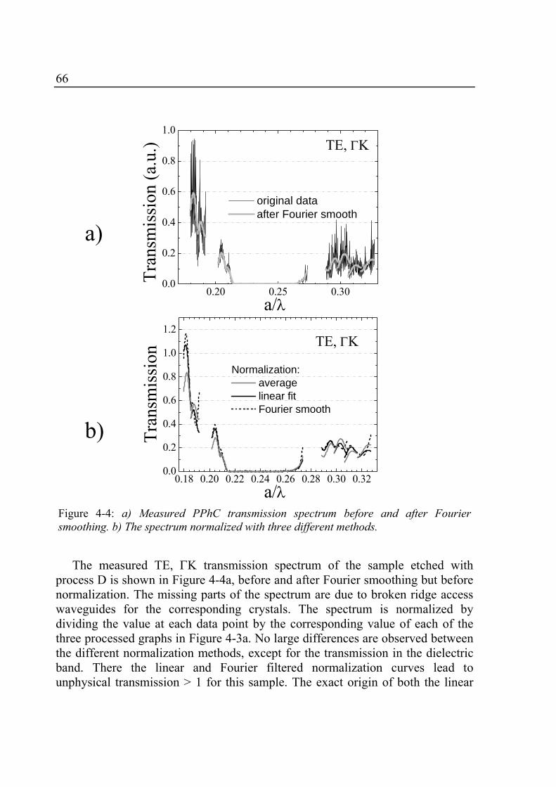
66
The measured TE, ΓK transmission spectrum of the sample etched with process D is shown in Figure 4-4a, before and after Fourier smoothing but before normalization. The missing parts of the spectrum are due to broken ridge access waveguides for the corresponding crystals. The spectrum is normalized by dividing the value at each data point by the corresponding value of each of the three processed graphs in Figure 4-3a. No large differences are observed between the different normalization methods, except for the transmission in the dielectric band. There the linear and Fourier filtered normalization curves lead to unphysical transmission > 1 for this sample. The exact origin of both the linear
0.20 0.25 0.300.0
0.2
0.4
0.6
0.8
1.0
original data after Fourier smooth
TE, ΓKTr
ansm
issi
on (a
.u.)
a/λ
0.18 0.20 0.22 0.24 0.26 0.28 0.30 0.320.0
0.2
0.4
0.6
0.8
1.0
1.2
Normalization: average linear fit Fourier smooth
TE, ΓK
Tra
nsm
issi
on
a/λ Figure 4-4: a) Measured PPhC transmission spectrum before and after Fourier smoothing. b) The spectrum normalized with three different methods.
a)
b)
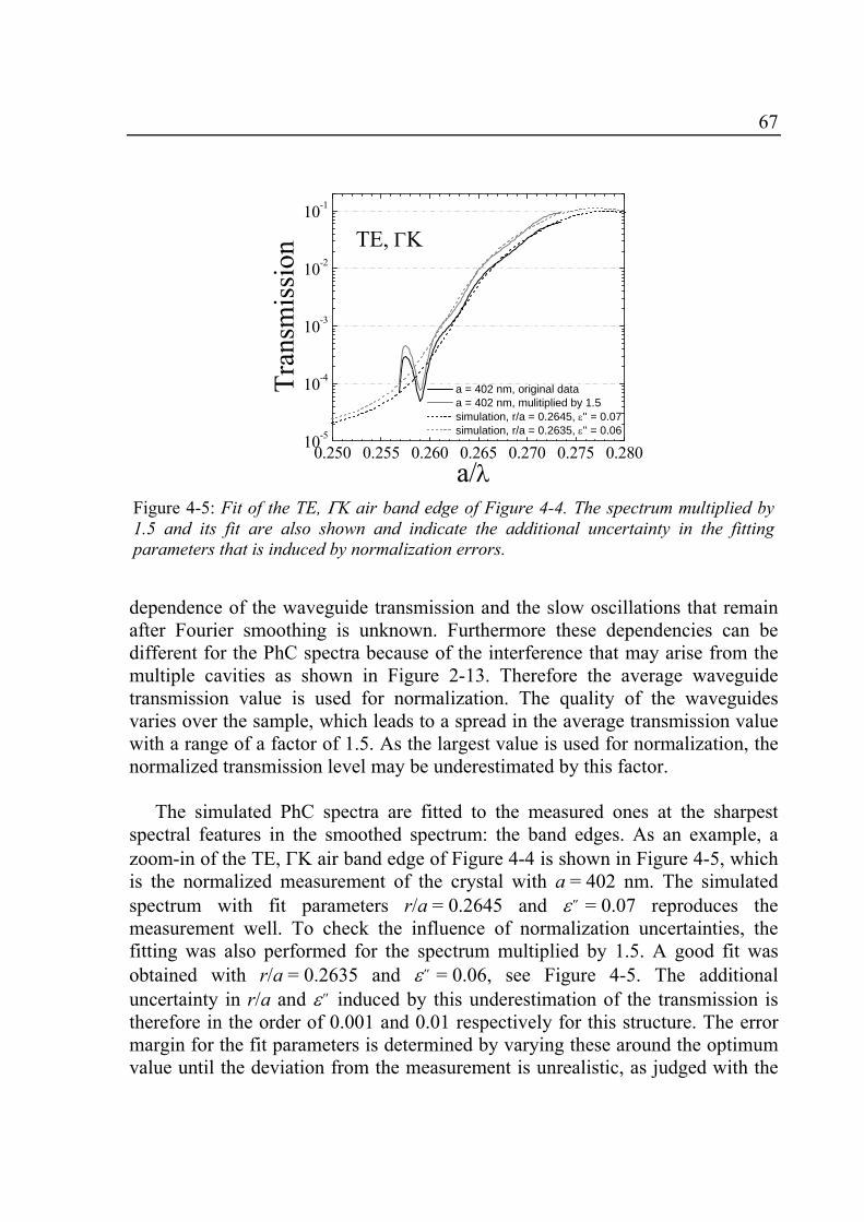
67
dependence of the waveguide transmission and the slow oscillations that remain after Fourier smoothing is unknown. Furthermore these dependencies can be different for the PhC spectra because of the interference that may arise from the multiple cavities as shown in Figure 2-13. Therefore the average waveguide transmission value is used for normalization. The quality of the waveguides varies over the sample, which leads to a spread in the average transmission value with a range of a factor of 1.5. As the largest value is used for normalization, the normalized transmission level may be underestimated by this factor.
The simulated PhC spectra are fitted to the measured ones at the sharpest
spectral features in the smoothed spectrum: the band edges. As an example, a zoom-in of the TE, ΓK air band edge of Figure 4-4 is shown in Figure 4-5, which is the normalized measurement of the crystal with a = 402 nm. The simulated spectrum with fit parameters r/a = 0.2645 and ε'' = 0.07 reproduces the measurement well. To check the influence of normalization uncertainties, the fitting was also performed for the spectrum multiplied by 1.5. A good fit was obtained with r/a = 0.2635 and ε'' = 0.06, see Figure 4-5. The additional uncertainty in r/a and ε'' induced by this underestimation of the transmission is therefore in the order of 0.001 and 0.01 respectively for this structure. The error margin for the fit parameters is determined by varying these around the optimum value until the deviation from the measurement is unrealistic, as judged with the
0.250 0.255 0.260 0.265 0.270 0.275 0.28010-5
10-4
10-3
10-2
10-1
a = 402 nm, original data a = 402 nm, mulitiplied by 1.5 simulation, r/a = 0.2645, ε'' = 0.07 simulation, r/a = 0.2635, ε'' = 0.06
TE, ΓK
Tra
nsm
issi
on
a/λ Figure 4-5: Fit of the TE, ΓK air band edge of Figure 4-4. The spectrum multiplied by 1.5 and its fit are also shown and indicate the additional uncertainty in the fitting parameters that is induced by normalization errors.
68
bare eye.
4.3 Results In Table 4-1, the basic characteristics of the samples evaluated are
summarized. All crystals were designed to have r/a = 0.30. Cross-sectional SEM views of the characteristic hole profile for these samples are shown in the following sections with the optical data. Also, the profile of a 10-20 µm wide trench is shown, indicating the quality of the ridge waveguides.
4.3.1 Conical holes with a sidewall angle of 3° and a lateral etch in the top part
Sample A1 was obtained from ICP etching process A, which is defined in Table 3-6. A heterostructure sample with test patterns was etched along with sample A. The cross-sectional SEM views of ~200 nm diameter holes and the wide trench are shown in Figure 4-6. The holes are conical from top to bottom, 2.2 µm deep and exhibit a 30 nm wide lateral etch in the top 300 nm. Because of the considerable sidewall angle of ~3°, the optical loss is expected to be high for
1 Original sample reference is MO139-S3B.
Table 4-1: Properties of the optical transmission samples.
Sample # (crystal
directions)
Lithotuning lattice constants (nm)
Hole depth (µm)
Hole shape
A (ΓK)
309, 325, 346, 361, 402, 446, 470, 496, 522, 551 2.2 conical (3°),
undercut (30 nm)
B (ΓK)
280, 293, 307, 321, 336, 352, 369, 386, 405, 424, 465, 486,
509, 533, 559, 585, 612 2.2 conical (1°),
undercut (40 nm)
C (ΓK and ΓM)
282, 299, 317, 337, 357, 379, 402, 427, 453, 481, 510, 541,
574, 609 3.4
cylindrical, constricted in core region
D (ΓK and ΓM)
250, 266, 282, 299, 317, 337, 357, 379, 402, 427, 453, 481,
510, 541, 574, 609 4.1 cylindrical
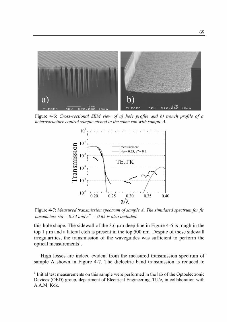
69
this hole shape. The sidewall of the 3.6 µm deep line in Figure 4-6 is rough in the top 1 µm and a lateral etch is present in the top 500 nm. Despite of these sidewall irregularities, the transmission of the waveguides was sufficient to perform the optical measurements1.
High losses are indeed evident from the measured transmission spectrum of
sample A shown in Figure 4-7. The dielectric band transmission is reduced to
1 Initial test measurements on this sample were performed in the lab of the Optoelectronic Devices (OED) group, department of Electrical Engineering, TU/e, in collaboration with A.A.M. Kok.
Figure 4-6: Cross-sectional SEM view of a) hole profile and b) trench profile of a heterostructure control sample etched in the same run with sample A.
0.20 0.25 0.30 0.35 0.4010-5
10-4
10-3
10-2
10-1
100
measurement r/a = 0.33, ε'' = 0.7
TE, ΓK
Tran
smis
sion
a/λ Figure 4-7: Measured transmission spectrum of sample A. The simulated spectrum for fit parameters r/a = 0.33 and ε'' = 0.65 is also included.
a) b)
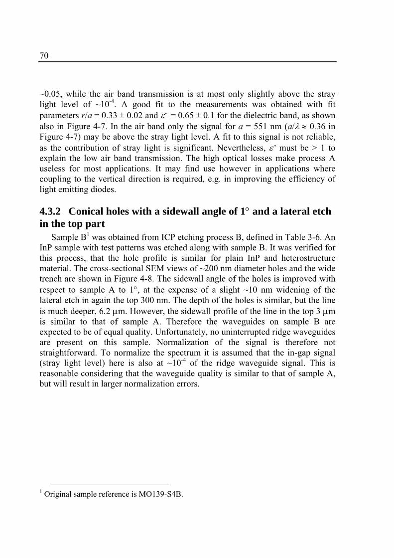
70
~0.05, while the air band transmission is at most only slightly above the stray light level of ~10-4. A good fit to the measurements was obtained with fit parameters r/a = 0.33 ± 0.02 and ε'' = 0.65 ± 0.1 for the dielectric band, as shown also in Figure 4-7. In the air band only the signal for a = 551 nm (a/λ ≈ 0.36 in Figure 4-7) may be above the stray light level. A fit to this signal is not reliable, as the contribution of stray light is significant. Nevertheless, ε'' must be > 1 to explain the low air band transmission. The high optical losses make process A useless for most applications. It may find use however in applications where coupling to the vertical direction is required, e.g. in improving the efficiency of light emitting diodes.
4.3.2 Conical holes with a sidewall angle of 1° and a lateral etch in the top part
Sample B1 was obtained from ICP etching process B, defined in Table 3-6. An InP sample with test patterns was etched along with sample B. It was verified for this process, that the hole profile is similar for plain InP and heterostructure material. The cross-sectional SEM views of ~200 nm diameter holes and the wide trench are shown in Figure 4-8. The sidewall angle of the holes is improved with respect to sample A to 1°, at the expense of a slight ~10 nm widening of the lateral etch in again the top 300 nm. The depth of the holes is similar, but the line is much deeper, 6.2 µm. However, the sidewall profile of the line in the top 3 µm is similar to that of sample A. Therefore the waveguides on sample B are expected to be of equal quality. Unfortunately, no uninterrupted ridge waveguides are present on this sample. Normalization of the signal is therefore not straightforward. To normalize the spectrum it is assumed that the in-gap signal (stray light level) here is also at ~10-4 of the ridge waveguide signal. This is reasonable considering that the waveguide quality is similar to that of sample A, but will result in larger normalization errors.
1 Original sample reference is MO139-S4B.
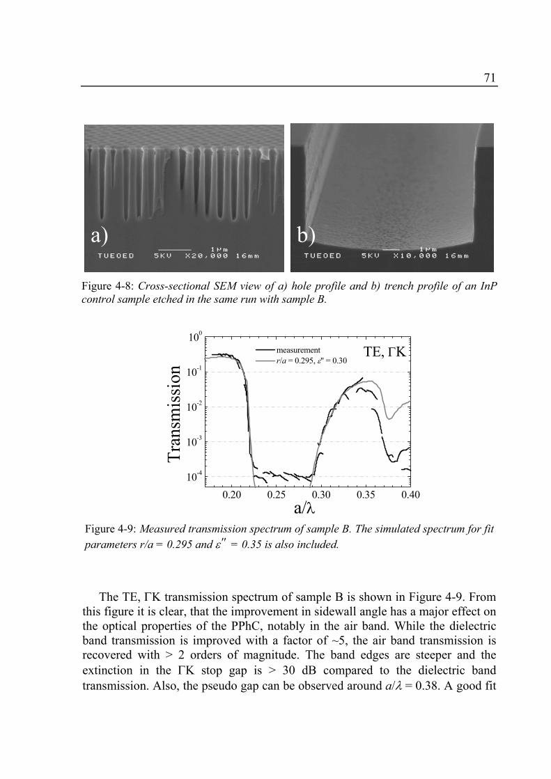
71
The TE, ΓK transmission spectrum of sample B is shown in Figure 4-9. From
this figure it is clear, that the improvement in sidewall angle has a major effect on the optical properties of the PPhC, notably in the air band. While the dielectric band transmission is improved with a factor of ~5, the air band transmission is recovered with > 2 orders of magnitude. The band edges are steeper and the extinction in the ΓK stop gap is > 30 dB compared to the dielectric band transmission. Also, the pseudo gap can be observed around a/λ = 0.38. A good fit
Figure 4-8: Cross-sectional SEM view of a) hole profile and b) trench profile of an InP control sample etched in the same run with sample B.
0.20 0.25 0.30 0.35 0.4010-4
10-3
10-2
10-1
100
measurement r/a = 0.295, ε'' = 0.30
TE, ΓK
Tran
smis
sion
a/λ
Figure 4-9: Measured transmission spectrum of sample B. The simulated spectrum for fit parameters r/a = 0.295 and ε'' = 0.35 is also included.
a) b)
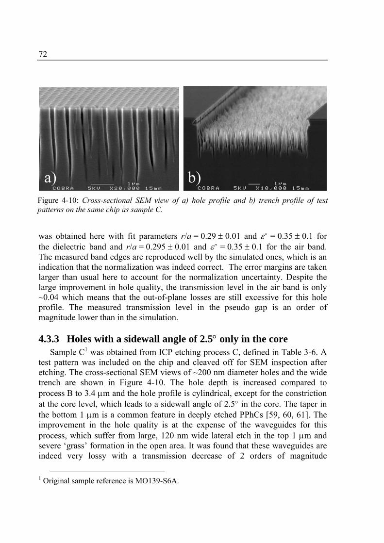
72
was obtained here with fit parameters r/a = 0.29 ± 0.01 and ε'' = 0.35 ± 0.1 for the dielectric band and r/a = 0.295 ± 0.01 and ε'' = 0.35 ± 0.1 for the air band. The measured band edges are reproduced well by the simulated ones, which is an indication that the normalization was indeed correct. The error margins are taken larger than usual here to account for the normalization uncertainty. Despite the large improvement in hole quality, the transmission level in the air band is only ~0.04 which means that the out-of-plane losses are still excessive for this hole profile. The measured transmission level in the pseudo gap is an order of magnitude lower than in the simulation.
4.3.3 Holes with a sidewall angle of 2.5° only in the core Sample C1 was obtained from ICP etching process C, defined in Table 3-6. A
test pattern was included on the chip and cleaved off for SEM inspection after etching. The cross-sectional SEM views of ~200 nm diameter holes and the wide trench are shown in Figure 4-10. The hole depth is increased compared to process B to 3.4 µm and the hole profile is cylindrical, except for the constriction at the core level, which leads to a sidewall angle of 2.5° in the core. The taper in the bottom 1 µm is a common feature in deeply etched PPhCs [59, 60, 61]. The improvement in the hole quality is at the expense of the waveguides for this process, which suffer from large, 120 nm wide lateral etch in the top 1 µm and severe ‘grass’ formation in the open area. It was found that these waveguides are indeed very lossy with a transmission decrease of 2 orders of magnitude
1 Original sample reference is MO139-S6A.
Figure 4-10: Cross-sectional SEM view of a) hole profile and b) trench profile of test patterns on the same chip as sample C.
a) b)
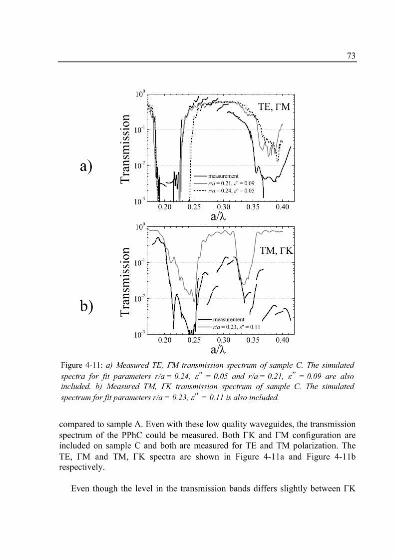
73
compared to sample A. Even with these low quality waveguides, the transmission spectrum of the PPhC could be measured. Both ΓK and ΓM configuration are included on sample C and both are measured for TE and TM polarization. The TE, ΓM and TM, ΓK spectra are shown in Figure 4-11a and Figure 4-11b respectively.
Even though the level in the transmission bands differs slightly between ΓK
0.20 0.25 0.30 0.35 0.4010-3
10-2
10-1
100
measurement r/a = 0.21, ε'' = 0.09 r/a = 0.24, ε'' = 0.05
TE, ΓM
Tran
smis
sion
a/λ
0.20 0.25 0.30 0.35 0.4010-3
10-2
10-1
100
measurement r/a = 0.23, ε'' = 0.11
TM, ΓK
Tran
smis
sion
a/λ
Figure 4-11: a) Measured TE, ΓM transmission spectrum of sample C. The simulated spectra for fit parameters r/a = 0.24, ε'' = 0.05 and r/a = 0.21, ε'' = 0.09 are also included. b) Measured TM, ΓK transmission spectrum of sample C. The simulated spectrum for fit parameters r/a = 0.23, ε'' = 0.11 is also included.
a)
b)
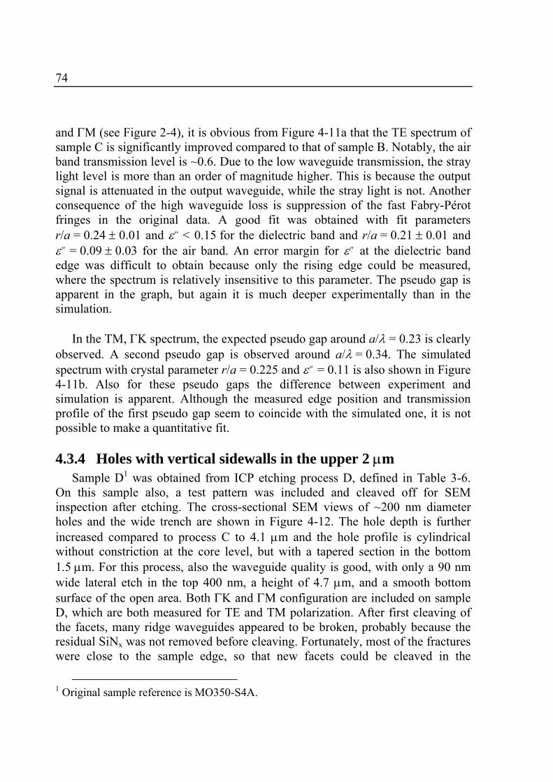
74
and ΓM (see Figure 2-4), it is obvious from Figure 4-11a that the TE spectrum of sample C is significantly improved compared to that of sample B. Notably, the air band transmission level is ~0.6. Due to the low waveguide transmission, the stray light level is more than an order of magnitude higher. This is because the output signal is attenuated in the output waveguide, while the stray light is not. Another consequence of the high waveguide loss is suppression of the fast Fabry-Pérot fringes in the original data. A good fit was obtained with fit parameters r/a = 0.24 ± 0.01 and ε'' < 0.15 for the dielectric band and r/a = 0.21 ± 0.01 and ε'' = 0.09 ± 0.03 for the air band. An error margin for ε'' at the dielectric band edge was difficult to obtain because only the rising edge could be measured, where the spectrum is relatively insensitive to this parameter. The pseudo gap is apparent in the graph, but again it is much deeper experimentally than in the simulation.
In the TM, ΓK spectrum, the expected pseudo gap around a/λ = 0.23 is clearly
observed. A second pseudo gap is observed around a/λ = 0.34. The simulated spectrum with crystal parameter r/a = 0.225 and ε'' = 0.11 is also shown in Figure 4-11b. Also for these pseudo gaps the difference between experiment and simulation is apparent. Although the measured edge position and transmission profile of the first pseudo gap seem to coincide with the simulated one, it is not possible to make a quantitative fit.
4.3.4 Holes with vertical sidewalls in the upper 2 µm Sample D1 was obtained from ICP etching process D, defined in Table 3-6.
On this sample also, a test pattern was included and cleaved off for SEM inspection after etching. The cross-sectional SEM views of ~200 nm diameter holes and the wide trench are shown in Figure 4-12. The hole depth is further increased compared to process C to 4.1 µm and the hole profile is cylindrical without constriction at the core level, but with a tapered section in the bottom 1.5 µm. For this process, also the waveguide quality is good, with only a 90 nm wide lateral etch in the top 400 nm, a height of 4.7 µm, and a smooth bottom surface of the open area. Both ΓK and ΓM configuration are included on sample D, which are both measured for TE and TM polarization. After first cleaving of the facets, many ridge waveguides appeared to be broken, probably because the residual SiNx was not removed before cleaving. Fortunately, most of the fractures were close to the sample edge, so that new facets could be cleaved in the
1 Original sample reference is MO350-S4A.
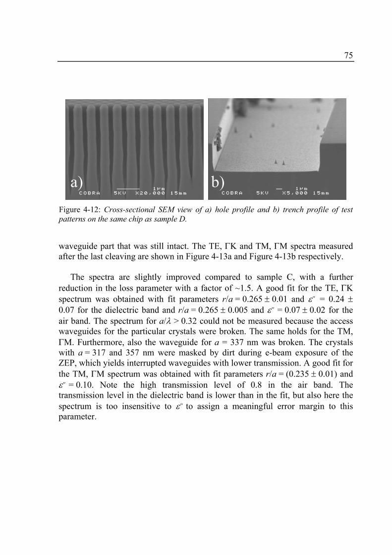
75
waveguide part that was still intact. The TE, ΓK and TM, ΓM spectra measured after the last cleaving are shown in Figure 4-13a and Figure 4-13b respectively.
The spectra are slightly improved compared to sample C, with a further
reduction in the loss parameter with a factor of ~1.5. A good fit for the TE, ΓK spectrum was obtained with fit parameters r/a = 0.265 ± 0.01 and ε'' = 0.24 ± 0.07 for the dielectric band and r/a = 0.265 ± 0.005 and ε'' = 0.07 ± 0.02 for the air band. The spectrum for a/λ > 0.32 could not be measured because the access waveguides for the particular crystals were broken. The same holds for the TM, ΓM. Furthermore, also the waveguide for a = 337 nm was broken. The crystals with a = 317 and 357 nm were masked by dirt during e-beam exposure of the ZEP, which yields interrupted waveguides with lower transmission. A good fit for the TM, ΓM spectrum was obtained with fit parameters r/a = (0.235 ± 0.01) and ε'' = 0.10. Note the high transmission level of 0.8 in the air band. The transmission level in the dielectric band is lower than in the fit, but also here the spectrum is too insensitive to ε'' to assign a meaningful error margin to this parameter.
Figure 4-12: Cross-sectional SEM view of a) hole profile and b) trench profile of test patterns on the same chip as sample D.
a) b)
76
4.4 Discussion A summary of the results is given in Table 4-2. Indicated are the lattice
constant for the crystal(s) under consideration, fit parameters r/a and ε'' , the calculated value for εint'' (see section 2.1.4) and εext'' as determined from εext'' = ε''
- εint'' . Because no reliable fit could be found for the measured TM, ΓK spectra,
0.20 0.25 0.30 0.3510-5
10-4
10-3
10-2
10-1
100
measurement r/a = 0.265, ε'' = 0.07 r/a = 0.265, ε'' = 0.24
TE, ΓKTr
ansm
issi
on
a/λ
0.15 0.20 0.25 0.30 0.3510-3
10-2
10-1
100
interrupted waveguides
measurement r/a = 0.235, ε'' 0.10
TM, ΓΜ
Tran
smis
sion
a/λ
Figure 4-13: a) Measured TE, ΓK transmission spectrum of sample D. The simulated spectra for fit parameters r/a = 0.265, ε'' = 0.24 and r/a = 0.265, ε'' = 0.07 are also included. b) Measured TM, ΓM transmission spectrum of sample D. The simulated spectrum for fit parameters r/a = 0.235, ε'' = 0.10 is also included.
a)
b)
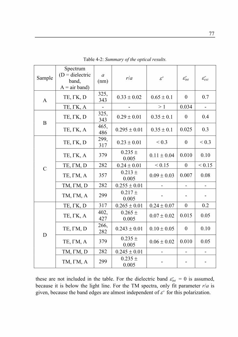
77
these are not included in the table. For the dielectric band εint'' = 0 is assumed, because it is below the light line. For the TM spectra, only fit parameter r/a is given, because the band edges are almost independent of ε'' for this polarization.
Table 4-2: Summary of the optical results.
Sample
Spectrum (D = dielectric
band, A = air band)
a (nm) r/a ε'' εint'' εext''
TE, ΓK, D 325, 343 0.33 ± 0.02 0.65 ± 0.1 0 0.7 A
TE, ΓK, A - - > 1 0.034 -
TE, ΓK, D 325, 343 0.29 ± 0.01 0.35 ± 0.1 0 0.4
B TE, ΓK, A 465,
486 0.295 ± 0.01 0.35 ± 0.1 0.025 0.3
TE, ΓK, D 299, 317 0.23 ± 0.01 < 0.3 0 < 0.3
TE, ΓK, A 379 0.235 ± 0.005 0.11 ± 0.04 0.010 0.10
TE, ΓM, D 282 0.24 ± 0.01 < 0.15 0 < 0.15
TE, ΓM, A 357 0.213 ± 0.005 0.09 ± 0.03 0.007 0.08
TM, ΓM, D 282 0.255 ± 0.01 - - -
C
TM, ΓM, A 299 0.217 ± 0.005 - - -
TE, ΓK, D 317 0.265 ± 0.01 0.24 ± 0.07 0 0.2
TE, ΓK, A 402, 427
0.265 ± 0.005 0.07 ± 0.02 0.015 0.05
TE, ΓM, D 266, 282 0.243 ± 0.01 0.10 ± 0.05 0 0.10
TE, ΓM, A 379 0.235 ± 0.005 0.06 ± 0.02 0.010 0.05
TM, ΓM, D 282 0.245 ± 0.01 - - -
D
TM, ΓM, A 299 0.235 ± 0.005 - - -
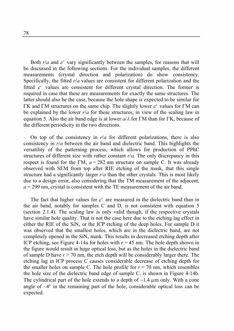
78
Both r/a and ε'' vary significantly between the samples, for reasons that will
be discussed in the following sections. For the individual samples, the different measurements (crystal direction and polarization) do show consistency. Specifically, the fitted r/a values are consistent for different polarization and the fitted ε'' values are consistent for different crystal direction. The former is required in case that these are measurements for exactly the same structures. The latter should also be the case, because the hole shape is expected to be similar for ΓK and ΓM structures on the same chip. The slightly lower ε'' values for ΓM can be explained by the lower r/a for these structures, in view of the scaling law in equation 5. Also the air band edge is at lower a/λ for ΓM than for ΓK, because of the different periodicity in the two directions.
On top of the consistency in r/a for different polarizations, there is also
consistency in r/a between the air band and dielectric band. This highlights the versatility of the patterning process, which allows for production of PPhC structures of different size with rather constant r/a. The only discrepancy in this respect is found for the ΓM, a = 282 nm structure on sample C. It was already observed with SEM from top after RIE etching of the mask, that this single structure had a significantly larger r/a than the other crystals. This is most likely due to a design error, also considering that the TM measurement of the adjacent, a = 299 nm, crystal is consistent with the TE measurement of the air band.
The fact that higher values for ε'' are measured in the dielectric band than in
the air band, notably for samples C and D, is not consistent with equation 5 (section 2.1.4). The scaling law is only valid though, if the respective crystals have similar hole quality. That is not the case here due to the etching lag effect in either the RIE of the SiNx or the ICP etching of the deep holes. For sample D it was observed that the smallest holes, which are in the dielectric band, are not completely opened in the SiNx mask. This results in decreased etching depth after ICP etching, see Figure 4-14a for holes with r = 45 nm. The hole depth shown in the figure would result in huge optical loss, but as the holes in the dielectric band of sample D have r > 70 nm, the etch depth will be considerably larger there. The etching lag in ICP process C causes considerable decrease of etching depth for the smaller holes on sample C. The hole profile for r = 70 nm, which resembles the hole size of the dielectric band edge of sample C, is shown in Figure 4-14b. The cylindrical part of the hole extends to a depth of ~1.4 µm only. With a cone angle of ~4° in the remaining part of the hole, considerable optical loss can be expected.
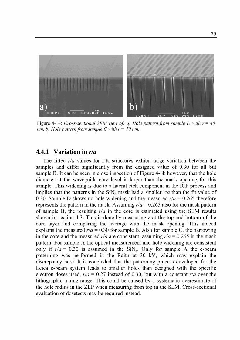
79
4.4.1 Variation in r/a The fitted r/a values for ΓK structures exhibit large variation between the
samples and differ significantly from the designed value of 0.30 for all but sample B. It can be seen in close inspection of Figure 4-8b however, that the hole diameter at the waveguide core level is larger than the mask opening for this sample. This widening is due to a lateral etch component in the ICP process and implies that the patterns in the SiNx mask had a smaller r/a than the fit value of 0.30. Sample D shows no hole widening and the measured r/a = 0.265 therefore represents the pattern in the mask. Assuming r/a = 0.265 also for the mask pattern of sample B, the resulting r/a in the core is estimated using the SEM results shown in section 4.3. This is done by measuring r at the top and bottom of the core layer and comparing the average with the mask opening. This indeed explains the measured r/a = 0.30 for sample B. Also for sample C, the narrowing in the core and the measured r/a are consistent, assuming r/a = 0.265 in the mask pattern. For sample A the optical measurement and hole widening are consistent only if r/a = 0.30 is assumed in the SiNx. Only for sample A the e-beam patterning was performed in the Raith at 30 kV, which may explain the discrepancy here. It is concluded that the patterning process developed for the Leica e-beam system leads to smaller holes than designed with the specific electron doses used, r/a = 0.27 instead of 0.30, but with a constant r/a over the lithographic tuning range. This could be caused by a systematic overestimate of the hole radius in the ZEP when measuring from top in the SEM. Cross-sectional evaluation of dosetests may be required instead.
Figure 4-14: Cross-sectional SEM view of: a) Hole pattern from sample D with r = 45 nm. b) Hole pattern from sample C with r = 70 nm.
a) b)
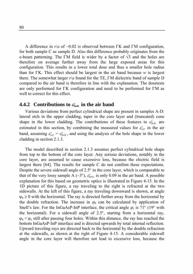
80
A difference in r/a of ~0.02 is observed between ΓK and ΓM configuration, for both sample C as sample D. Also this difference probably originates from the e-beam patterning. The ΓM field is wider by a factor of √3 and the holes are therefore on average further away from the large exposed areas for this configuration. This results in a lower total dose and thus a smaller hole radius than for ΓK. This effect should be largest in the air band because w is largest there. The somewhat larger r/a found for the TE, ΓM dielectric band of sample D compared to the air band is therefore in line with the explanation. The dosetests are only performed for ΓK configuration and need to be performed for ΓM as well to correct for this effect.
4.4.2 Contributions to εhole'' in the air band Various deviations from perfect cylindrical shape are present in samples A-D:
lateral etch in the upper cladding, taper in the core layer and (truncated) cone shape in the lower cladding. The contributions of these features to εhole'' are estimated in this section, by combining the measured values for εext'' in the air band, assuming εext'' = εhole'' , and using the analysis of the hole shape in the lower cladding in section 2.1.3.
The model described in section 2.1.3 assumes perfect cylindrical hole shape
from top to the bottom of the core layer. Any serious deviations, notably in the core layer, are assumed to cause excessive loss, because the electric field is largest there [64]. The results for sample C do not confirm these expectations. Despite the severe sidewall angle of 2.5° in the core layer, which is comparable to that of the very lossy sample A (~3°), εhole'' is only 0.09 in the air band. A possible explanation for this based on geometric optics is illustrated in Figure 4-15. In the 1D picture of this figure, a ray traveling to the right is refracted at the two sidewalls. At the left of this figure, a ray traveling downward is shown, at angle ϕh ≥ 0 with the horizontal. The ray is directed further away from the horizontal by the double refraction. The increase in ϕh can be calculated by application of Snell’s law. For the InGaAsP-InP interface, the critical angle ϕc is 71° (19° with the horizontal). For a sidewall angle of 2.5°, starting from a horizontal ray, ϕh < ϕc still after passing four holes. Within this distance, the ray has reached the bottom InGaAsP-InP interface and is directed upwards by total internal reflection. Upward traveling rays are directed back to the horizontal by the double refraction at the sidewalls, as shown at the right of Figure 4-15. A considerable sidewall angle in the core layer will therefore not lead to excessive loss, because the
81
refracted light is recaptured. The contribution to εhole'' of the lateral etch in the upper cladding can now be
estimated using the optical results for sample B and the discussion above. In view of the results for sample C, the small sidewall angle in the core would lead to a contribution << 0.1 to εhole'' for this sample. In the bottom cladding, the hole has truncated cone shape with h = 2.2 µm and β = 1°, with can be estimated from Figure 2-7 to contribute ~0.05 to εhole'' . Therefore it is concluded that the lateral etch in the upper cladding leads to εhole'' ≈ 0.3.
Sample A exhibits a similar lateral etch as sample B, hence it is assumed that
it contributes ~0.3 to εhole'' for this sample also. The hole profile in the core is similar to sample C, so this may add ~0.1 to εhole'' for sample A. The part of the hole in the lower cladding has simple cone shape with β = 3° so its contribution to εhole'' can be estimated from Figure 2-7 to be 0.3. These contributions add up to εhole'' = 0.7, which is equal to the measured value in the dielectric band. For these high values of ε'' and with n' fixed to 1 in the simulation it can be deduced from equation 2, that ε' < 0.9. It is therefore questionable if the perturbative approach and the scaling laws derived from it are still valid in this regime. Even if they were, simple application of the scaling law is not straightforward here, because the quality of the holes may differ for the dielectric band and the air band. Also, the uncertainties in εhole'' are high. A deviation of 1° in the sidewall angle in the lower cladding leads to a difference of 0.2 in εhole'' . For these reasons, a reliable
Figure 4-15: Light refracted in the core by holes with non-vertical sidewalls are recaptured in the core: geometric optics illustration for a sidewall angle of 3°.
82
quantitative comparison of sample A with the other samples is not possible. The fitted value of εhole'' ≈ 0.05 in the air band for sample D cannot be
explained from the tapered profile in the bottom part of the hole, judged from Figure 2-7. Most likely it is caused by the local fluctuations in hole radius and sidewall angle that are visible for the holes in Figure 4-12a, notably the slight widening just below the core. The loss parameter value found here is comparable to those reported for ICP etched PPhCs (ε'' = 0.056 [58]) and close to those reported for PPhCs etched with CAIBE (ε'' = 0.045 [136]) for the InP material system. This highlights the versatility of the Cl2/O2- chemistry used for the ICP etching, although the r/a value and the combination of hole shape and vertical waveguide structure must be taken into account for a precise comparison [136].
4.4.3 Pseudo gaps Pseudo gaps for different polarization and crystal direction are observed for
sample B, C and D. In all cases, they could not be accurately reproduced in the FDTD simulation, the measured transmission level being significantly lower. Recall that the cause of the pseudo gaps is the symmetry mismatch between the waveguide mode and the PhC mode. When the access waveguides are removed in the simulation and plane wave input is used, the simulated transmission level in the pseudo gap decreases with 2-3 orders of magnitude. The fundamental difference is that the symmetry mismatch is present along the entire input for plane wave excitation, while it is strictly valid only at the centerline of the waveguide in case of excitation with the eigenmode of a ridge waveguide. Coupling to the anti-symmetric PhC mode is possible, probably due to the significant field gradient towards the edges of the ridge. This could also explain the discrepancy between experiment and simulation because the under etch causes a difference between the two at the edge of the ridge. Experimentally the intensity may be lower at the waveguide edge, because the light is scattered away by the imperfections there. Consequently, the experimental transmission is lower than simulated. The decrease of the in gap transmission with frequency for TM, ΓK, was also observed in the similar measurements of ref. [15] and is reproduced in the simulation.
4.5 Conclusion End-fire transmission measurements are performed for both polarizations on
deeply etched InP-based PPhCs with different hole quality. 2D FDTD
83
calculations, in which optical losses are simulated by a fictitious absorption in the holes, are fit to the optical measurements using r/a and ε'' (the imaginary component of the dielectric constant in the holes) as free parameters.
For all samples, the r/a value found for the dielectric band is similar to that of
the air band. Also it was deduced from a comparison with SEM results that the pattern in the SiNx mask has r/a = 0.27 for all samples patterned with the Leica 5000 e-beam pattern generator. This indicates that the patterned r/a is rather constant over the lithographic tuning range and for different samples and highlights the reproducibility of the patterning process. The deviation from the design value of r/a = 0.30 may be due to a systematic overestimation of the hole radius in the SEM evaluation of EBL dosetests from top.
The out-of-plane losses induced by imperfect hole shape are evaluated for the
different samples using εhole'' as a figure of merit. This hole shape induced loss parameter is obtained from the measured ε'' and the calculated extrinsic loss parameter εint'' . The values for εhole'' found for the air band are consistent for the ΓK- and ΓM-oriented crystals on the same chip, which are expected to have similar hole shape. This indicates that the εhole'' values found are reliable. The εhole'' values for the dielectric band compared to the air band do not satisfy the usual scaling with r/a and a/λ. This is due to the lower quality of the holes with smaller r in the dielectric band, caused by the RIE-lag in either the mask opening or the ICP etching of the holes.
It was shown that a considerable sidewall of 2.5° in the core layer does not
lead to excessive losses, in contrast to the common belief that cylindrical hole shape in the core is imperative. Qualitatively, this is probably due to recapture of the refracted light in the core. Using this knowledge, the contribution to εhole'' of a ~40 nm wide lateral etch in the top 300 nm is estimated to be ~0.3. A value for εhole'' as low as 0.05 was found for the best quality PPhC. This is similar to values reported in the literature by other groups for deeply etched InP-based PPhCs.
Significant transmission within the ΓK stop gap was observed both in
simulation and experiment. It is shown that this is due to the finite width of the input waveguide, which causes diffraction into allowed crystal directions. Light can travel through the crystal by continuous diffraction into allowed directions and a significant part is captured by the output waveguide, even if the forward direction is forbidden.
84
Chapter 5 Filling the air holes
The functionality of PPhC structures is increased when their optical properties
are dynamically tunable by external means as heat and electric, magnetic or optical fields. In practice this can be achieved in semiconductor based PPhCs by adjusting the refractive index of either the high- or low index part, although tuning using micro-electro-mechanical systems [137], deformation [138, 139], or an atomic force microscope tip [140], is also reported. Tuning of PPhCs using the high index has been proposed [141, 142] and demonstrated [143], but the properties of this material are usually dictated by the (active) application. An attractive possibility is therefore infiltration of the air holes with an organic material that has a tunable refractive index. This allows for increased design freedom, because the properties of the semiconductor and the infill can be independently optimized for the application.
An important material class in this respect comprises liquid crystals (LCs), in
particular the nematic type, because these materials exhibit large birefringence; ∆n = 0.2-0.3 for a conventional LC like 5CB, but much higher values are also reported [144]. Since the first proposal of Busch and John [145], several tuning proposals and experiments and have been reported with 1D [146, 147, 148, 149],
85
2D [109, 150, 151, 152, 153, 154], 3D (see ref. 155 for an overview) and planar [71, 72, 73, 74, 75, 76] LC-infiltrated PhCs. Also, device proposals based on LC tuning have appeared in the literature [156, 157, 158, 159, 160], although the only experimental demonstration so far is the PhC laser of refs. [72, 73]. The tuning speed of LCs is limited to ms, down to µs for certain ferroelectric or polymer-dispersed LCs [161], because it relies on the physical reordering of molecules. This is sufficient for many applications, but higher speeds are required for e.g. signal modulation in the backbone of optical networks. Furthermore, the liquid state could prevent certain applications or limit the compatibility with other processing steps. Therefore also other materials, notably electro-optically active or optically non-linear (NLO) polymers must also be considered as tunable low-index material.
The possible tuning speed of NLO polymers is intrinsically high (< ps) [162].
The achievable ∆n is rather low however, so that cavities with considerable Q are probably required [149]. In a recent proposal, the Kerr-nonlinearity of a polymer infiltrated in a 1D PhC was used to realize a Q-switched laser [163]. Also, the filling of 2D PhC lasers with photoaddressable polymer has been proposed [73]. Apart from the active application, also the passive effect of the refractive index change has many applications. In contrast to membrane type structures [72], the infiltration of deeply etched photonic crystals is expected to increase the vertical confinement due to improved index guiding, which was used to decrease the diffraction loss of a 1D PhC laser [164]. Furthermore, it was recently shown that selective filling opens up a new way to create components like single mode waveguides, waveguide bends, crossings and splitters from “bulk” 2D PhCs [165, 166]. Although the latter two applications are also possible with LC filling, the solid polymer offers better mechanical stability of the devices. Also, after planarization of infiltrated structures, further polymer processing may be used to create extra functionality above the PhC.
5.1 Infiltration parameters A schematic cross-section of a fluid column in a cylinder with submicron
diameter is shown in Figure 5-1. For these dimensions the capillary action is dominant and the gravitational force is negligible [167]. The capillary pressure pcap thus provides the driving force for the liquid flow and is given by:
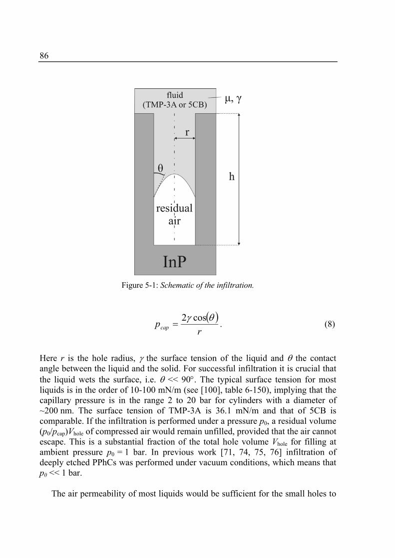
86
( )
rpcap
θγ cos2= . (8)
Here r is the hole radius, γ the surface tension of the liquid and θ the contact angle between the liquid and the solid. For successful infiltration it is crucial that the liquid wets the surface, i.e. θ << 90°. The typical surface tension for most liquids is in the order of 10-100 mN/m (see [100], table 6-150), implying that the capillary pressure is in the range 2 to 20 bar for cylinders with a diameter of ~200 nm. The surface tension of TMP-3A is 36.1 mN/m and that of 5CB is comparable. If the infiltration is performed under a pressure p0, a residual volume (p0/pcap)Vhole of compressed air would remain unfilled, provided that the air cannot escape. This is a substantial fraction of the total hole volume Vhole for filling at ambient pressure p0 = 1 bar. In previous work [71, 74, 75, 76] infiltration of deeply etched PPhCs was performed under vacuum conditions, which means that p0 << 1 bar.
The air permeability of most liquids would be sufficient for the small holes to
Figure 5-1: Schematic of the infiltration.
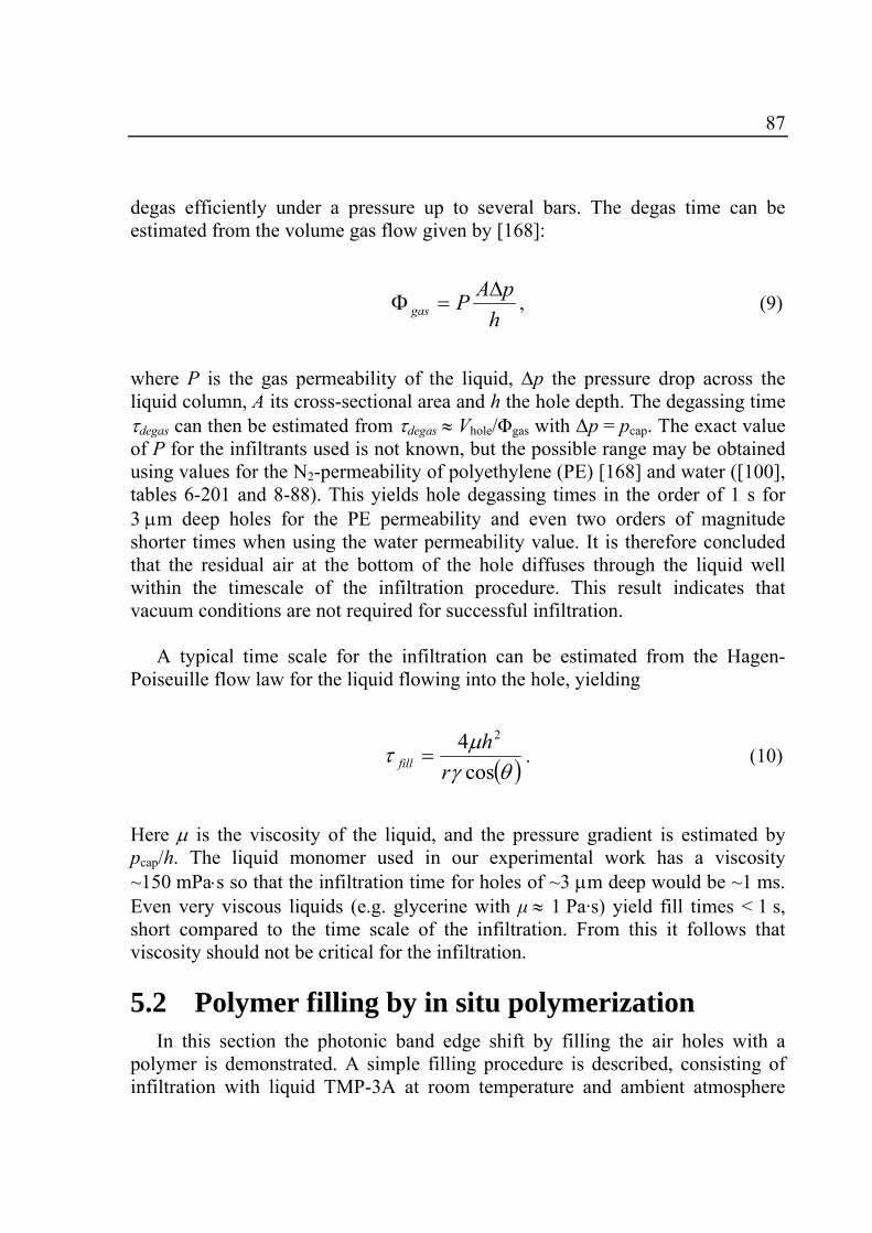
87
degas efficiently under a pressure up to several bars. The degas time can be estimated from the volume gas flow given by [168]:
h
pAPgas∆
=Φ , (9)
where P is the gas permeability of the liquid, ∆p the pressure drop across the liquid column, A its cross-sectional area and h the hole depth. The degassing time τdegas can then be estimated from τdegas ≈ Vhole/Φgas with ∆p = pcap. The exact value of P for the infiltrants used is not known, but the possible range may be obtained using values for the N2-permeability of polyethylene (PE) [168] and water ([100], tables 6-201 and 8-88). This yields hole degassing times in the order of 1 s for 3 µm deep holes for the PE permeability and even two orders of magnitude shorter times when using the water permeability value. It is therefore concluded that the residual air at the bottom of the hole diffuses through the liquid well within the timescale of the infiltration procedure. This result indicates that vacuum conditions are not required for successful infiltration.
A typical time scale for the infiltration can be estimated from the Hagen-
Poiseuille flow law for the liquid flowing into the hole, yielding
( )θγµτcos
4 2
rh
fill = . (10)
Here µ is the viscosity of the liquid, and the pressure gradient is estimated by pcap/h. The liquid monomer used in our experimental work has a viscosity ~150 mPa⋅s so that the infiltration time for holes of ~3 µm deep would be ~1 ms. Even very viscous liquids (e.g. glycerine with µ ≈ 1 Pa·s) yield fill times < 1 s, short compared to the time scale of the infiltration. From this it follows that viscosity should not be critical for the infiltration.
5.2 Polymer filling by in situ polymerization In this section the photonic band edge shift by filling the air holes with a
polymer is demonstrated. A simple filling procedure is described, consisting of infiltration with liquid TMP-3A at room temperature and ambient atmosphere
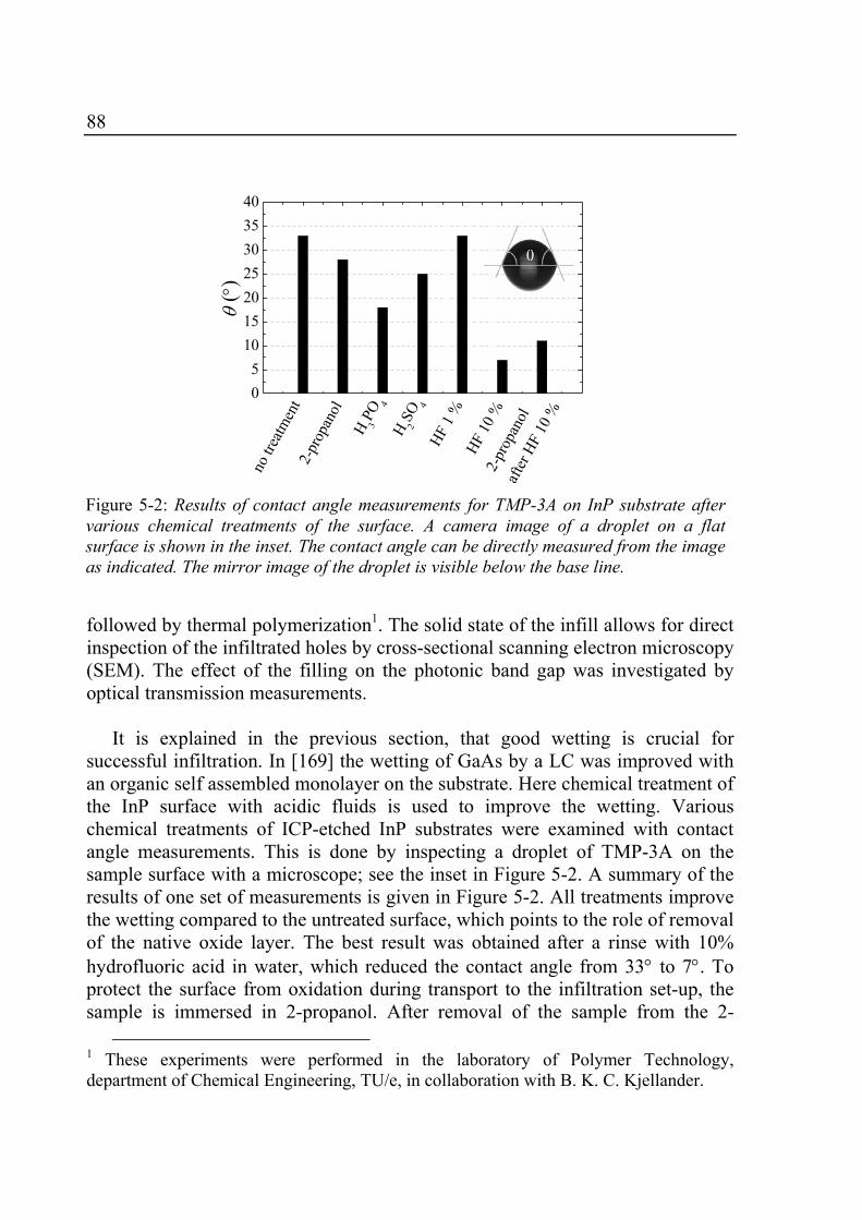
88
followed by thermal polymerization1. The solid state of the infill allows for direct inspection of the infiltrated holes by cross-sectional scanning electron microscopy (SEM). The effect of the filling on the photonic band gap was investigated by optical transmission measurements.
It is explained in the previous section, that good wetting is crucial for successful infiltration. In [169] the wetting of GaAs by a LC was improved with an organic self assembled monolayer on the substrate. Here chemical treatment of the InP surface with acidic fluids is used to improve the wetting. Various chemical treatments of ICP-etched InP substrates were examined with contact angle measurements. This is done by inspecting a droplet of TMP-3A on the sample surface with a microscope; see the inset in Figure 5-2. A summary of the results of one set of measurements is given in Figure 5-2. All treatments improve the wetting compared to the untreated surface, which points to the role of removal of the native oxide layer. The best result was obtained after a rinse with 10% hydrofluoric acid in water, which reduced the contact angle from 33° to 7°. To protect the surface from oxidation during transport to the infiltration set-up, the sample is immersed in 2-propanol. After removal of the sample from the 2-
1 These experiments were performed in the laboratory of Polymer Technology, department of Chemical Engineering, TU/e, in collaboration with B. K. C. Kjellander.
05
10152025303540
θ (°
)
2-pr
opan
olaf
ter H
F 10
%
HF 10
%
HF 1
%
H 2SO
4
H 3PO
4
2-pr
opan
ol
no tr
eatm
ent
Figure 5-2: Results of contact angle measurements for TMP-3A on InP substrate after various chemical treatments of the surface. A camera image of a droplet on a flat surface is shown in the inset. The contact angle can be directly measured from the image as indicated. The mirror image of the droplet is visible below the base line.
89
propanol and blow-dry of the surface, the measured contact angle is still 11°. The wetting depends on the exact chemical state of the surface and the ambient atmosphere. This causes a considerable spread in the measured contact angles over different sets of experiments. In a separate set, even a contact angle of 3° was measured after surface treatment with HF and 2-propanol.
After the surface preparation, a droplet of the liquid monomer is deposited
onto the sample to cover the hole pattern, either in vacuum (20 mbar) or ambient atmosphere, at room temperature. The thermal polymerization is performed on a hotplate under N2 flow, to minimize oxygen reaction with the radicals formed. To suppress formation of cracks in the polymer layer, the temperature is gradually increased from room temperature up to 50 oC, where polymerization is allowed for 10 minutes. The temperature is further increased to 70 oC in order to increase the mobility of the unreacted monomers and the sample was baked for 20 minutes at this temperature to complete the polymerization. The refractive index of the polymer was measured separately by spectroscopic ellipsometry on a layer that was spin-cast on a Si-substrate and subsequently polymerized. For wavelengths around 1550 nm the measured refractive index is 1.465 ± 0.005; the absorption in this wavelength region is negligible for our purpose.
Figure 5-3: Cross-sectional SEM-view of ~200 nm diameter holes filled with poly-TMP-3A, with infiltration at a pressure of a) 20 mbar and b) ambient atmosphere.
a) b)
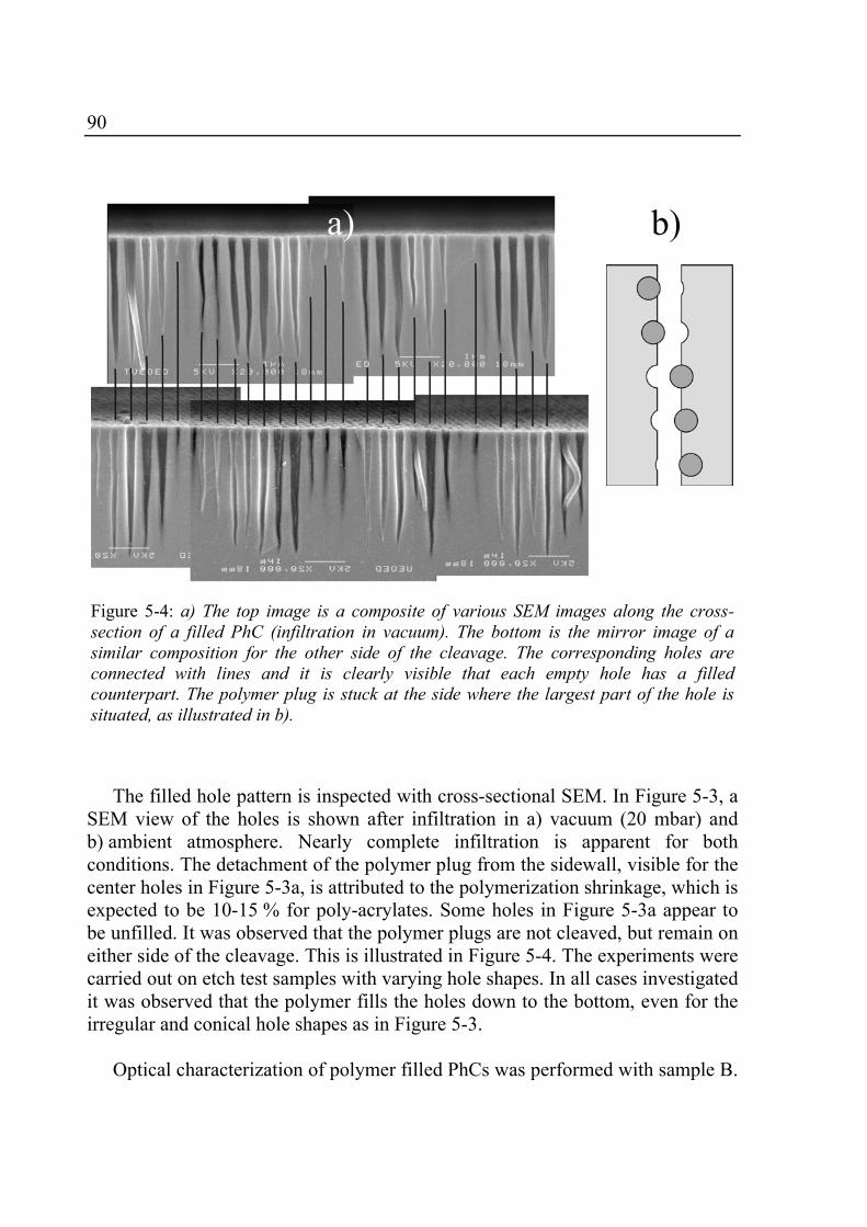
90
The filled hole pattern is inspected with cross-sectional SEM. In Figure 5-3, a
SEM view of the holes is shown after infiltration in a) vacuum (20 mbar) and b) ambient atmosphere. Nearly complete infiltration is apparent for both conditions. The detachment of the polymer plug from the sidewall, visible for the center holes in Figure 5-3a, is attributed to the polymerization shrinkage, which is expected to be 10-15 % for poly-acrylates. Some holes in Figure 5-3a appear to be unfilled. It was observed that the polymer plugs are not cleaved, but remain on either side of the cleavage. This is illustrated in Figure 5-4. The experiments were carried out on etch test samples with varying hole shapes. In all cases investigated it was observed that the polymer fills the holes down to the bottom, even for the irregular and conical hole shapes as in Figure 5-3.
Optical characterization of polymer filled PhCs was performed with sample B.
Figure 5-4: a) The top image is a composite of various SEM images along the cross-section of a filled PhC (infiltration in vacuum). The bottom is the mirror image of a similar composition for the other side of the cleavage. The corresponding holes are connected with lines and it is clearly visible that each empty hole has a filled counterpart. The polymer plug is stuck at the side where the largest part of the hole is situated, as illustrated in b).
a) b)
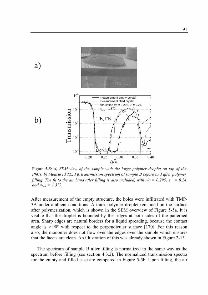
91
After measurement of the empty structure, the holes were infiltrated with TMP-3A under ambient conditions. A thick polymer droplet remained on the surface after polymerization, which is shown in the SEM overview of Figure 5-5a. It is visible that the droplet is bounded by the ridges at both sides of the patterned area. Sharp edges are natural borders for a liquid spreading, because the contact angle is > 90° with respect to the perpendicular surface [170]. For this reason also, the monomer does not flow over the edges over the sample which ensures that the facets are clean. An illustration of this was already shown in Figure 2-13.
The spectrum of sample B after filling is normalized in the same way as the
spectrum before filling (see section 4.3.2). The normalized transmission spectra for the empty and filled case are compared in Figure 5-5b. Upon filling, the air
0.20 0.25 0.30 0.35 0.4010-4
10-3
10-2
10-1
100
TE, ΓK
measurement empty crystal measurement filled crystal simulation r/a = 0.295, ε'' = 0.24,
nhole = 1.372
Tran
smis
sion
a/λ
Figure 5-5: a) SEM view of the sample with the large polymer droplet on top of the PhCs. b) Measured TE, ΓK transmission spectrum of sample B before and after polymer filling. The fit to the air band after filling is also included, with r/a = 0.295, ε'' = 0.24 and nhole = 1.372.
b)
a)
92
band edge exhibits a redshift of one third of the stop gap width, which is the optical evidence for hole filling under ambient conditions. No significant shift is observed for the dielectric band edge, because the electric field of the Bloch mode is located primarily in the semiconductor material [75, 150]. It was discussed in the previous chapter, that the r/a value of sample B is rather constant over the lithographic tuning range and it is therefore assumed to be 0.295 also for the air band edge of the filled sample. The filling efficiency η (volume of polymer plug divided by hole volume) is determined by fitting the air band edge to simulations with fit parameters ε'' and nhole, the latter being the average refractive index inside the hole. The filling efficiency is then calculated via η = (nhole-1)/(npolymer-1), where npolymer is the refractive index of the polymer. Holes with incomplete filling are thus approximated in the simulation by a uniform material with an average refractive index nhole = 1 + η(npolymer - 1). It has been verified with band structure calculations for a more realistic distribution of the refractive index, i.e. a polymer cylinder in the hole centre surrounded by a sheet of air, that this approximation is indeed valid here. The polymer filling reduces the average refraction angle at the semiconductor-hole interface (see Figure 4-15) and thus also the out-of-plane losses. This effect is not taken into account in the 2D simulation implicitly, so that the value of ε'' for the empty structure is no longer valid for the filled. A good fit to the measurements is obtained with ε'' = 0.24 ± 0.05 and nhole = 1.37 ± 0.05, leading to a filling efficiency of 0.8 ± 0.1. This number is consistent with complete infiltration of the holes followed by polymerization shrinkage of 10-15 %. The filling yields an important decrease of the loss parameter, from to 0.35 to 0.24, which leads to improvement of the air band transmission with a factor of > 2.
5.3 Polymer filling by solvent evaporation Polymer e-beam resists (EBRs) as PMMA and ZEP are usually deposited onto
a substrate by spincoating from solution. A solid polymer layer is then obtained by thermal evaporation of the solvent. In this section, a first experiment to fill the PPhC holes with EBR from solution is described. This would create interesting possibilities, because it can be expected that removal of the infill from selected individual holes is possible with a subsequent EBL step. Such a process could be used to fabricate devices as described in refs. [34] and [165] with the EBR fill itself, or using the structure as a template for further infiltration steps as in section 5.2. Repetition of the latter procedure could make the filling of adjacent holes with different materials possible, to create for instance the optimized waveguide crossing design of ref. [34]. If appropriate holes are filled with NLO polymer, the
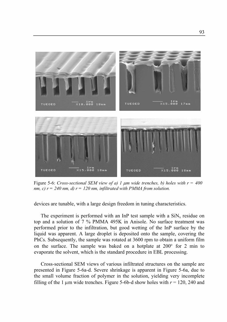
93
devices are tunable, with a large design freedom in tuning characteristics. The experiment is performed with an InP test sample with a SiNx residue on
top and a solution of 7 % PMMA 495K in Anisole. No surface treatment was performed prior to the infiltration, but good wetting of the InP surface by the liquid was apparent. A large droplet is deposited onto the sample, covering the PhCs. Subsequently, the sample was rotated at 3600 rpm to obtain a uniform film on the surface. The sample was baked on a hotplate at 200° for 2 min to evaporate the solvent, which is the standard procedure in EBL processing.
Cross-sectional SEM views of various infiltrated structures on the sample are
presented in Figure 5-6a-d. Severe shrinkage is apparent in Figure 5-6a, due to the small volume fraction of polymer in the solution, yielding very incomplete filling of the 1 µm wide trenches. Figure 5-6b-d show holes with r = 120, 240 and
Figure 5-6: Cross-sectional SEM view of a) 1 µm wide trenches, b) holes with r = 400 nm, c) r = 240 nm, d) r = 120 nm, infiltrated with PMMA from solution.
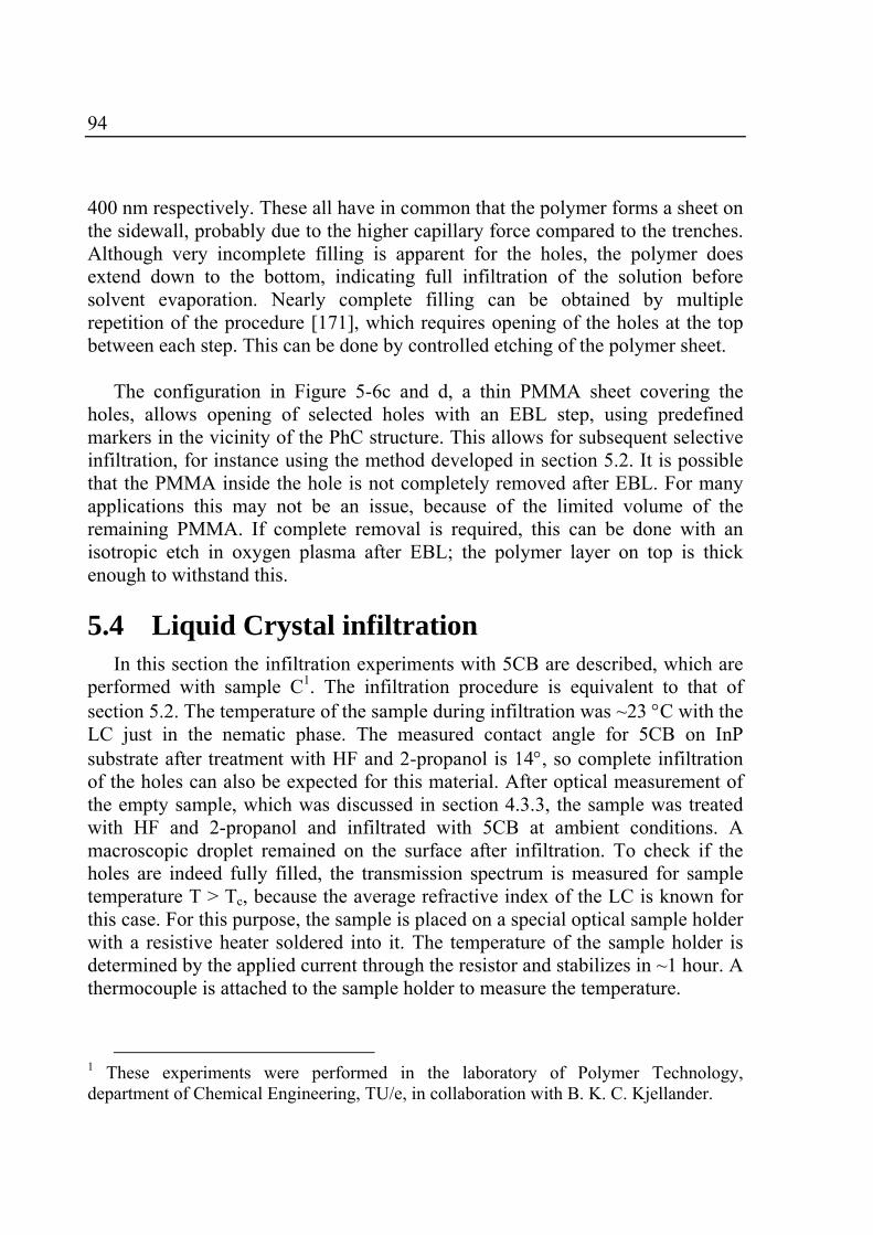
94
400 nm respectively. These all have in common that the polymer forms a sheet on the sidewall, probably due to the higher capillary force compared to the trenches. Although very incomplete filling is apparent for the holes, the polymer does extend down to the bottom, indicating full infiltration of the solution before solvent evaporation. Nearly complete filling can be obtained by multiple repetition of the procedure [171], which requires opening of the holes at the top between each step. This can be done by controlled etching of the polymer sheet.
The configuration in Figure 5-6c and d, a thin PMMA sheet covering the
holes, allows opening of selected holes with an EBL step, using predefined markers in the vicinity of the PhC structure. This allows for subsequent selective infiltration, for instance using the method developed in section 5.2. It is possible that the PMMA inside the hole is not completely removed after EBL. For many applications this may not be an issue, because of the limited volume of the remaining PMMA. If complete removal is required, this can be done with an isotropic etch in oxygen plasma after EBL; the polymer layer on top is thick enough to withstand this.
5.4 Liquid Crystal infiltration In this section the infiltration experiments with 5CB are described, which are
performed with sample C1. The infiltration procedure is equivalent to that of section 5.2. The temperature of the sample during infiltration was ~23 °C with the LC just in the nematic phase. The measured contact angle for 5CB on InP substrate after treatment with HF and 2-propanol is 14°, so complete infiltration of the holes can also be expected for this material. After optical measurement of the empty sample, which was discussed in section 4.3.3, the sample was treated with HF and 2-propanol and infiltrated with 5CB at ambient conditions. A macroscopic droplet remained on the surface after infiltration. To check if the holes are indeed fully filled, the transmission spectrum is measured for sample temperature T > Tc, because the average refractive index of the LC is known for this case. For this purpose, the sample is placed on a special optical sample holder with a resistive heater soldered into it. The temperature of the sample holder is determined by the applied current through the resistor and stabilizes in ~1 hour. A thermocouple is attached to the sample holder to measure the temperature.
1 These experiments were performed in the laboratory of Polymer Technology, department of Chemical Engineering, TU/e, in collaboration with B. K. C. Kjellander.
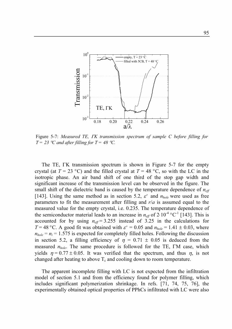
95
The TE, ΓK transmission spectrum is shown in Figure 5-7 for the empty
crystal (at T = 23 °C) and the filled crystal at T = 48 °C, so with the LC in the isotropic phase. An air band shift of one third of the stop gap width and significant increase of the transmission level can be observed in the figure. The small shift of the dielectric band is caused by the temperature dependence of neff [143]. Using the same method as in section 5.2, ε'' and nhole were used as free parameters to fit the measurement after filling and r/a is assumed equal to the measured value for the empty crystal, i.e. 0.235. The temperature dependence of the semiconductor material leads to an increase in neff of 2⋅10-4 °C-1 [143]. This is accounted for by using neff = 3.255 instead of 3.25 in the calculations for T = 48 °C. A good fit was obtained with ε'' = 0.05 and nhole = 1.41 ± 0.03, where nhole = ni = 1.575 is expected for completely filled holes. Following the discussion in section 5.2, a filling efficiency of η = 0.71 ± 0.05 is deduced from the measured nhole. The same procedure is followed for the TE, ΓM case, which yields η = 0.77 ± 0.05. It was verified that the spectrum, and thus η, is not changed after heating to above Tc and cooling down to room temperature.
The apparent incomplete filling with LC is not expected from the infiltration
model of section 5.1 and from the efficiency found for polymer filling, which includes significant polymerization shrinkage. In refs. [71, 74, 75, 76], the experimentally obtained optical properties of PPhCs infiltrated with LC were also
0.18 0.20 0.22 0.24 0.2610-3
10-2
10-1
100
TE, ΓΚ
empty, T = 23 °C filled with 5CB, T = 48 °C
Tran
smis
sion
a/λ
Figure 5-7: Measured TE, ΓK transmission spectrum of sample C before filling for T = 23 °C and after filling for T = 48 °C.
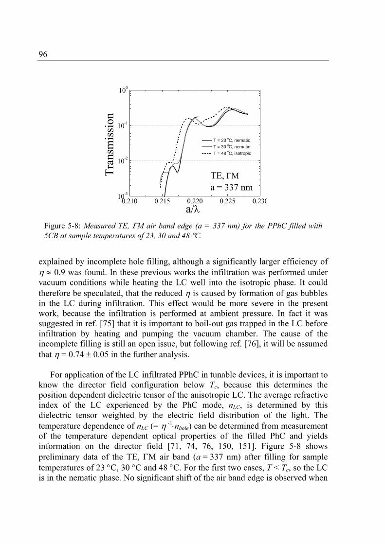
96
explained by incomplete hole filling, although a significantly larger efficiency of η ≈ 0.9 was found. In these previous works the infiltration was performed under vacuum conditions while heating the LC well into the isotropic phase. It could therefore be speculated, that the reduced η is caused by formation of gas bubbles in the LC during infiltration. This effect would be more severe in the present work, because the infiltration is performed at ambient pressure. In fact it was suggested in ref. [75] that it is important to boil-out gas trapped in the LC before infiltration by heating and pumping the vacuum chamber. The cause of the incomplete filling is still an open issue, but following ref. [76], it will be assumed that η = 0.74 ± 0.05 in the further analysis.
For application of the LC infiltrated PPhC in tunable devices, it is important to
know the director field configuration below Tc, because this determines the position dependent dielectric tensor of the anisotropic LC. The average refractive index of the LC experienced by the PhC mode, nLC, is determined by this dielectric tensor weighted by the electric field distribution of the light. The temperature dependence of nLC (= η -1⋅nhole) can be determined from measurement of the temperature dependent optical properties of the filled PhC and yields information on the director field [71, 74, 76, 150, 151]. Figure 5-8 shows preliminary data of the TE, ΓM air band (a = 337 nm) after filling for sample temperatures of 23 °C, 30 °C and 48 °C. For the first two cases, T < Tc, so the LC is in the nematic phase. No significant shift of the air band edge is observed when
0.210 0.215 0.220 0.225 0.23010-3
10-2
10-1
100
Tran
smis
sion
a/λ
TE, ΓΜa = 337 nm
T = 23 oC, nematic T = 30 oC, nematic T = 48 oC, isotropic
Figure 5-8: Measured TE, ΓM air band edge (a = 337 nm) for the PPhC filled with 5CB at sample temperatures of 23, 30 and 48 °C.
97
heating the sample from T = 23 °C, which is just above Tnc, to T = 30 °C. This indicates that the order parameter is constant at least in a certain temperature range above Tnc. A similar behavior was shown for the eutectic LC mixture E7 infiltrated in macroporous silicon in ref. [150]. When the temperature is further increased to 48 °C, so well above Tc, the air band exhibits a redshift of ∆a/λ = 0.001. It is calculated that part of this shift, ∆a/λ = 3⋅10-4, is induced by the increase in neff. The change in nLC due to the nematic-to-isotropic phase transition therefore contributes to the redshift with an amount of ∆a/λ = 7⋅10-4. The direction of the shift indicates that nLC < ni when the LC is in the nematic phase. This would rule out the PP configuration of the director field, see Figure 2-18, because for this configuration and TE polarized light nLC is expected to be approximately the in-plane average 1/2(no
2 + ne2 )1/2 (1.601 for 5CB), i.e. larger
than ni. Fitting of the air band for T < Tc yields nhole = 1.37 ± 0.03 for ΓK and
nhole = 1.41 ± 0.03 for ΓM for the LC in the nematic phase. Within the experimental uncertainties, these values are the same as found for the LC in the isotropic phase. Also, the temperature dependent measurements have not been done in sufficient detail to follow the exact temperature dependence of nhole. Therefore, no quantitative conclusions can be drawn on the absolute values of nLC that are deduced from nhole. Keeping this in mind, nLC, is determined to be 1.50 ± 0.04 for ΓK- and 1.55 ± 0.04 for ΓM-structures. These values are close to no, which would indicate that the mesogens are oriented primarily perpendicular to the plane. For AX director field and TE polarized light, nLC is simply no, but for ER configuration nLC is a complex average of the position dependent dielectric tensor. It was discussed in ref. [150], that the electric field of the air band PhC mode is located primarily in the center of the holes, where the mesogens are aligned along the hole axis for both AX and ER configuration. Therefore, it is in general not straightforward to distinguish between the two director fields with this type of measurements. In the present work in particular, the experimental uncertainties are too large for this purpose. A larger r/a would lead to larger shifts and a smaller error in nLC. It is expected that additional information can be obtained from measurements with TM polarized light [76].
Although the exact director field is not known, the thermal tuning range for
this PPhC infiltrated with 5CB is directly visible in Figure 5-8. The total corresponding wavelength shift is 7 nm, of which 5 nm due to the tuning of nLC. The total band edge shift leads to a factor of ~10 difference in transmission level
98
due to the exponential decrease at the air band edge. This is achieved by heating the sample from 30 °C to above 48 °C so a temperature change of 18 °C would be enough for 10 dB extinction of an optical signal. The thermal tuning range of the LC may be enhanced by increasing r/a or using LCs with larger birefringence.
5.5 Conclusion InP based deeply etched PPhCs have been filled with both polymer and liquid
crystal. An important step in the filling procedure is infiltration of the holes with a liquid, either the monomer as precursor for the polymer or the LC itself. It was estimated that the infiltration time is << 1 s. The entrapped air at the bottom of the hole is estimated to diffuse out through the liquid on a timescale < 1 s. From these estimations it is expected that the holes are fully infiltrated even at ambient conditions.
Polymer filling is obtained by thermal polymerization of the infiltrated
monomer, trimethylolpropane triacrylate. The filled PhCs were inspected with SEM and complete filling down to the bottom of the hole was observed, both for samples infiltrated in vacuum and in ambient atmosphere. With optical transmission measurements it was observed that the polymer filling induces a shift of the air band edge of one third of the stop gap width. From the fit of 2D FDTD simulations a filling efficiency of 0.8 ± 0.1 was deduced, proving nearly complete filling. The deviation from complete filling is caused by polymerization shrinkage, which is typically 10-15 % for polyacrylates.
Filling with polymer e-beam resist was investigated with a first experiment by
infiltration from solution and subsequent evaporation of the solvent. The low fraction of polymer in solution leads to very incomplete filling of the holes, order of 10 %. It was observed with SEM that the polymer is situated on the sidewall and that a sheet with a thickness of a few hundred nm covers the PhC. This may open the way to filling of selected holes by opening the sheet in defined areas with an EBL step and subsequent filling of the opened hole(s).
The PPhCs filled with the LC 4-pentyl-4-cyanobiphenyl were investigated
with optical transmission measurements. The air band shift due to the filling is again one third of the stop gap width. The 2D FDTD simulations fit to the measurement with the LC in the isotropic phase, yield a filling efficiency of 0.74 ± 0.05. This incomplete filling is not expected and requires further investigation. In the preliminary temperature dependent measurements

99
performed, the experimental uncertainties are too large to conclude on the director field configuration of the LC inside the holes. However, the experiments do show thermal shift of the air band of ∆λ = 7 nm, which is partly caused by the semiconductor (~2 nm) and partly by the LC (~5 nm).
100
Summary
The subject of this thesis is deeply etched planar photonic crystals (PPhCs) in InP material for eventual application in photonic integrated circuits. The PPhCs consist of a two-dimensional periodic pattern of holes etched through a standard InP/InGaAsP/InP planar waveguide layer stack. The periodic refractive index acts on light waves in a similar way as the periodic potential in a solid crystal acts on electron waves, yielding photonic band gaps. PPhCs with a photonic band gap centered at the telecom wavelength of 1550 nm are investigated in this thesis, which implies that the air holes have a diameter d of ~200 nm and are arranged in a (hexagonal) lattice with a lattice constant a of ~400 nm.
A Cl2-based inductively coupled plasma etching process is developed for
fabrication of the PPhCs, using a SiNx layer patterned with e-beam lithography and subsequent reactive ion etching as a mask. For low optical loss it is important that the etched holes exhibit vertical and straight sidewalls to a depth of at least 2 µm. The concept of sidewall passivation is exploited to promote this verticality. For this purpose, relatively small amounts of O2 or N2 are added to the Cl2 flow into the plasma. With a proper Cl2/O2 flow ratio, here ~14/3, good quality holes are obtained for a significantly larger window in parameter space, notably concerning sample temperature, than for Cl2-only chemistry. At this Cl2/O2 flow ratio, the temperature dependence of the large area etch rate is determined by the surface chemistry of the InP-Cl2 system. The sample temperature should therefore be raised sufficiently (typically > 200 °C) to reach the regime where the InCl3 corrosion layer formed evaporates from the etched surface. To improve the stability of the sample temperature, the heating by the ion bombardment must be compensated by cooling the carrier wafer with a He-gas backflow. With an optimized process, high aspect ratio holes with d = 200 nm are etched in 1 minute to a depth > 3.5 µm with vertical sidewalls in the upper 2 µm.
Optical characterization of the fabricated PPhCs is performed with an end-fire
technique. For this purpose, the hole-patterns are monolithically integrated with ridge waveguides in a transmission configuration and the samples are cleaved to obtain end facets. Light from a polarization controlled tunable diode laser (wavelength range 1470-1570 nm) is coupled into and out of the waveguides with microscope objectives. Transmission spectra were obtained on a normalized frequency scale by measurement of PPhCs with various a on the same chip. Photonic band gaps are clearly observed, with an extinction of >30 dB compared
101
to the transmission bands. It is observed that significant transmission is still possible when the forward direction is forbidden (i.e. the frequency of the incoming light is in the stop gap), probably by continuous diffraction into directions that are allowed. The measurements are compared to two-dimensional finite difference time domain calculations, in which the out-of-plane losses are simulated by an artificial absorption in the holes. The imaginary component of the dielectric constant that is related to this absorption, referred to as loss parameter ε'' , and the ratio of hole radius over lattice constant r/a are used as free parameters to fit the calculated spectra to the measured spectra. The fitted loss parameter is a figure of merit for the quality of the etched holes. Hole qualities resulting from four different etch processes are evaluated and loss parameters ranging from 0.7 down to 0.05 are obtained. An important conclusion is that a significant sidewall angle in the core of the planar waveguide does not lead to excessive losses, as long as the sidewalls are vertical in the claddings. Analysis of the fitted r/a values shows that the patterning process is reproducible.
The application area of PPhC structures will be greatly enhanced when their
optical properties are tunable. An attractive possibility to achieve the desired tuning is filling of the air holes with a material that has a tunable refractive index. Solid polymer fills are obtained by infiltration with a liquid monomer and subsequent in situ thermal polymerization. Infiltration of PPhCs with a liquid relies on the capillary forces in the holes. Complete filling is obtained even in ambient atmosphere, as long as the wetting of the InP by the liquid is good. Residual air under the fluid column disappears from the holes by diffusion through the liquid. It was observed with scanning electron microscopy that all holes are filled down the bottom, for infiltration both under vacuum conditions and in ambient atmosphere. Upon filling of the PPhC with a polymer, the measured air band edge exhibits a redshift, yielding a 30 % decrease of the stop gap. The filling degree is determined from fitting two-dimensional finite difference time domain calculations to the measured spectrum, using the refractive index in the hole and ε'' as free parameters. From this analysis, the filling degree is determined to be approximately 0.8, which is consistent with complete infiltration by the monomer followed by the expected 10-15 % polymerization shrinkage. Preliminary tuning experiments were performed with PPhCs infiltrated with liquid crystal. The sample was heated to above the nematic-to-isotropic phase transition temperature of the liquid crystal. This caused a wavelength shift of the photonic band edge with a magnitude of 7 nm, which is partly caused by refractive index change of the semiconductor (~2 nm) and partly by that of the liquid crystal (~5 nm).
102
Nederlandse samenvatting
Dit proefschrift gaat over diep geëtste planaire fotonische kristallen (PFKs) in InP materiaal voor uiteindelijke toepassing in fotonische geïntegreerde circuits. De PFKs bestaan uit een tweedimensionaal gatenpatroon, geëtst in een standaard InP/InGaAsP/InP planaire golfgeleider. Door de periodieke brekingsindex bezitten deze kristallen een zogenaamde fotonische ‘band gap’, analoog aan het bestaan van een elektronische ‘band gap’ in halfgeleiders. In dit proefschrift zijn PFKs onderzocht met een fotonische ‘band gap’ gecentreerd rond de telecom golflengte van 1550 nm, wat betekent dat de gaten een diameter d van ~200 nm hebben en zijn geordend in een (hexagonaal) rooster met een roosterconstante a van ~400 nm.
Een inductief gekoppeld plasma etsproces met reactief Cl2 is ontwikkeld voor
fabricage van de PFKs. Een SiNx-laag, gestructureerd met elektronstraal lithografie en daaropvolgend reactief ion etsen, is hierbij gebruikt als masker. Lage optische verliezen zijn alleen haalbaar als de zijwanden van de gaten recht en vertikaal zijn tot een diepte van tenminste 2 µm. Zijwandpassivatie is toegepast voor het bevorderen van de verticaliteit van de gaten. Voor dit doel zijn relatief kleine hoeveelheden O2 of N2 toegevoegd aan het Cl2-debiet in het plasma. Met de juiste Cl2/O2-debietverhouding, hier ~14/3, is de kwaliteit van de geëtste gaten goed in een groter deel van de ets parameterruimte, in het bijzonder wat betreft de temperatuur van het sample, vergeleken met puur Cl2 chemie. Voor deze Cl2/O2-debietverhouding is de temperatuursafhankelijkheid van de etssnelheid van grote vlakken bepaald door de oppervlaktechemie van het InP-Cl2 systeem. De temperatuur van het sample moet daarom voldoende hoog zijn (typisch > 200 °C) om de gevormde InCl3 corrosielaag te laten verdampen van het oppervlak. Om de stabiliteit van de temperatuur van het sample te verbeteren moet de verhitting door het ionenbombardement gecompenseerd worden door koeling van de sampledrager met He-gas aan de achterzijde. Met een geoptimaliseerd proces zijn gaten met d = 200 nm geëtst tot een diepte van 3.5 µm, met verticale zijwanden in de bovenste 2 µm.
Optische karakterisatie van de vervaardigde PFKs is gedaan met een
zogenoemde ‘end-fire’ techniek. Voor dit doel zijn de gatpatronen monolithisch geïntegreerd met golfgeleiders in een transmissie configuratie en zijn de samples gekliefd voor het verkrijgen van eindfacetten. Licht van een verstembare diode laser (golflengtebereik 1470-1570 nm) wordt in- en uit de golfgeleiders
103
gekoppeld met microscoopobjectieven. Transmissiespectra zijn verkregen op een genormeerde frequentieschaal door meting van PFKs met verschillende a op dezelfde chip. Fotonische ‘stop gaps’ zijn duidelijk zichtbaar, met een extinctie van > 30 dB vergeleken met de transmissiebanden. Significante transmissie is waargenomen voor de situatie waarbij de voorwaartse richting verboden is, oftewel in de ‘stop gap’ voor het inkomende licht. Dit is mogelijk, waarschijnlijk door continue diffractie in richtingen die wel zijn toegestaan. De metingen zijn vergeleken met tweedimensionale ‘finite difference time domain’ berekeningen, waarin de verliezen uit het vlak gesimuleerd zijn door een kunstmatige absorptie in de gaten. De imaginaire component van de diëlectrische constante die gerelateerd is aan deze absorptie, de zogenoemde verliesparameter ε'' , en de verhouding van de gatstraal tot de roosterconstante r/a zijn hierbij gebruikt als vrije parameters om de berekeningen overeen te laten komen met de experimenten. De aldus verkregen verliesparameter is een maat voor de kwaliteit van de gaten. Gatkwaliteiten resulterend van vier verschillende etsprocessen zijn geëvalueerd en verliesparameters variërend van 0.7 tot 0.05 zijn gevonden. Een belangrijke conclusie is dat een significante zijwandhoek in de kern van de planaire golfgeleider niet leidt tot excessieve verliezen, zo lang de zijwanden vertikaal zijn in de bekleding. Uit de analyse van de gevonden r/a waarden volgt dat het proces van de patroongeneratie reproduceerbaar is.
Verstembaarheid van de optische eigenschappen van PFKs zal het
toepassingsgebied van deze structuren aanzienlijk verruimen. Een aantrekkelijke mogelijkheid om de gewenste verstemming te bereiken is het vullen van de gaten met een materiaal dat een verstembare brekingsindex heeft. Vaste polymeervulling is verkregen door infiltratie met een vloeibare monomeer gevolgd door in situ thermische polymerisatie. De drijvende kracht voor infiltratie van PFKs is de capillaire werking van de vloeistof in de gaten. Complete vulling is verkregen zelfs in omgevingsatmosfeer, zolang de benatting van het InP door de vloeistof goed was. De overblijvende lucht onder de vloeistofkolom verdwijnt via diffusie door de vloeistof. Met elektronenmicroscopie is waargenomen dat de gaten tot op de bodem gevuld zijn, zowel onder vacuümomstandigheden als in omgevingsatmosfeer. Door de polymeervulling ondergaat de gemeten flank van de luchtband een roodverschuiving, die resulteert in een 30 % afname van de ‘stop gap’. De vulgraad is bepaald aan de hand van het aanpassen van tweedimensionale ‘finite difference time domain’ berekeningen aan de metingen, waarbij de brekingsindex in het gat en ε'' zijn gebruikt als vrije parameters. Uit deze analyse volgt een vulgraad van ongeveer 0.8, wat consistent is met volledige infiltratie door de monomeer gevolgd door de verwachte 10-15 %

104
polymerisatiekrimp. PFKs geïnfiltreerd met vloeibaar kristal zijn gebruikt voor eerste verstemmings experimenten. Het sample is verhit tot boven de nematisch-naar-isotroop fase overgangstemperatuur van het vloeibaar kristal. Dit veroorzaakte een golflengteverschuiving van de fotonische bandflank ter grootte van 7 nm, deels veroorzaakt door de verandering in brekingsindex van de halfgeleider (~2 nm) en deels door die van het vloeibaar kristal (~5 nm).

105
106
List of publications
Journal papers
R. van der Heijden, C. F. Carlström, J. A. P. Snijders, R. W. van der Heijden, F. Karouta, R . Nötzel and H. W. M. Salemink, B. K. C. Kjellander, C. W. M. Bastiaansen, D. J. Broer, and E. van der Drift, InP-based two-dimensional photonic crystals filled with polymers, Appl. Phys. Lett. 88, 161112 (2006).
C. F. Carlström, R. van der Heijden, F. Karouta, E. van der Drift, R. W. van der Heijden, and H. W. M. Salemink, Cl2/O2-inductively coupled plasma etching of deep hole-type photonic crystals in InP, J. Vac. Sci. Technol. B 24, L6 (2006).
Publication of the results in chapter 4 is in preparation. Conference papers Rob van der Heijden, Charlotte Kjellander, Carl-Fredrik Carlström, Juri Snijders, Harm Kicken, Rob W. van der Heijden, Cees Bastiaansen, Dick Broer, Fouad Karouta, Richard Nötzel, Emile van der Drift, and Huub Salemink, InP-based planar photonic crystals infiltrated with solid polymers and liquid crystals, Proc. SPIE 6322 (2006). Carl-Fredrik Carlström, Rob van der Heijden, Charlotte Kjellander, Rob W. van der Heijden, Cees Bastiaansen, Dick Broer, Fouad Karouta, Richard Nötzel, Emile van der Drift, and Huub Salemink, Deep hole InP photonic crystals infiltrated with solid polymers and liquid crystals, Proc. 28th International Conference on the Physics of Semiconductors, Vienna, Austria (2006). Rob van der Heijden, Charlotte Kjellander, Carl-Fredrik Carlström, Juri Snijders, Rob W. van der Heijden, Cees Bastiaansen, Dick Broer, Fouad Karouta, Richard Nötzel, Emile van der Drift, and Huub W.M. Salemink, Two-dimensional photonic crystals from semiconductor material with polymer filled holes, Proc. SPIE 6182 (2006).
107
R. van der Heijden, C.F. Carlström, E. van der Drift, R.W. van der Heijden, R. Nötzel, R. van Veldhoven, F. Karouta, H.W.M. Salemink, and A. Talneau, Cl2/O2- and Cl2/N2-based inductively coupled plasma etching of photonic crystals in InP: sidewall passivation, Proc. 17th Indium Phosphide and Related Materials Conference, Glasgow, Ireland (2005).
C. F. Carlström, R. van der Heijden, A. A. M. Kok, R.W van der Heijden, F. Karouta, J. J. G. M. van der Tol, R. Nötzel, P. J. van Veldhoven, and H.W.M. Salemink, Inductively coupled plasma etching of deep photonic crystal holes in InP using Cl2, Proc. 17th Indium Phosphide and Related Materials Conference, Glasgow, Ireland (2005).
Rob van der Heijden, Mischa S. P. Andriesse, Carl-Fredrik Carlström, Emile van der Drift, Erik-Jan Geluk, Rob W. van der Heijden, Fouad Karouta, Peter Nouwens, Y. Siang Oei, Tjibbe de Vries, and Huub W. M. Salemink, Deep dry etching process development for photonic crystals in InP-based planar waveguides, Proc. SPIE 5450, 523 (2004).
108
Dankwoord
Het promotieonderzoek en in het bijzonder het schrijven van een proefschrift is een grote inspanning. Een inspanning die ik zonder de, al dan niet expliciete, hulp van anderen nooit op deze manier had kunnen doen. Daarbij horen zeker ook de mensen van wie ik soms cruciale inzichten heb verworven via publicaties of discussies en de mensen in hun omgeving die dat weer mogelijk hebben gemaakt. De ruimte hier is te beperkt om al deze mensen met name te bedanken, maar ik wilde ze niet onvernoemd laten. Wel is er hier ruimte om de mensen in mijn omgeving te bedanken die veel voor mij en mijn promotieonderzoek betekend hebben. Ik heb sterk de behoefte om deze mensen in de schijnwerpers te zetten; daarom is het schrijven van een dankwoord ook zo leuk Ik kan en wil niet anders dan beginnen met promotor Huub Salemink, de man die het hele onderzoek mogelijk heeft gemaakt. Zijn inspanningen voor de (personele) groei van het project en het vertrouwen dat ik van hem heb gekregen zijn cruciaal geweest voor het slagen van mijn promotie. Cruciaal is ook de rol geweest van co-promotor en naamgenoot Rob van der Heijden als klankbord en mentor. Zijn fysisch inzicht en het daaruit voortkomende vermogen om met eenvoudige berekeningentjes zinvolle schattingen te maken blijven mij verbazen. Nog zo’n cruciaal persoon is Carl-Fredrik Carlström. Door zijn komst kwam de ontwikkeling van de technologie in een stroomversnelling en aan hem heb ik dan ook een groot deel van hoofdstuk 3 te danken. Bovendien is hij tot de verhuizing naar de D-vleugel een fijne kamergenoot geweest. Juri Snijders, eerste kamergenoot in D1.11 heeft als afstudeerder een groot deel van het werk van hoofdstuk 5 gedaan. Het doet me goed dat het project in de personen van promovendus en kamergenoot Harm Kicken en post-doc Christina Christova ook na mijn promotie een toekomst heeft. Ik zal het pepermuntjesritueel met Harm missen, misschien kan ik het een toekomstige kamergenoot aanleren. Afstudeerder Erik Roeling heeft zich de laatste maanden een waardevol kamergenoot getoond, alleen jammer dat hij geen pepermuntjes lust. Naast mijn kamergenoten hebben ook de groepsleden van PSN, voormalig HGF, me op verschillende manieren geholpen en bijgedragen aan een prettige werksfeer. Steun en toeverlaat van de groep Margriet van Doorne weet altijd de praktische (bureaucratische) zaken te regelen, biedt op zijn tijd een luisterend oor en is de motor van de sociale activiteiten. Van de promovendi wil ik graag ‘generatiegenoten’ Erik Bogaart, Twan van Lippen, Andrei Yakunin, Dilna Sreenivisan en Guido Quax noemen, we zaten tenslotte in hetzelfde schuitje. Het
109
weekje in Blaesheim met Dilna zal ik niet gauw vergeten. Twan heeft me vanaf de externe stage achtervolgd (of ik hem), ik ben benieuwd waar we na onze promotie terecht gaan komen. De technici in de groep zijn me, zonder uitzondering, behulpzaam geweest. Mede-Tilburger Peter Nouwens wil ik graag noemen vanwege zijn betrokkenheid bij het project. René van Veldhoven heeft de plakken gegroeid die zijn gebruikt voor de optische experimenten. In de eerste twee jaar van mijn promotie heb ik het grootste deel van de tijd doorgebracht in de Nanofacility groep van Emile van der Drift in Delft. Zijn kennis over de technologie en de beschikbaarheid van de cleanroom van DIMES hebben de ontwikkeling van het etsproces een vliegende start gegeven. Marc Zuiddam heeft me wegwijs gemaakt in de cleanroom. De hulp van Mischa Andriesse met de ICP is onmisbaar geweest. Ook Gilles Gobreau en Michiel Blauw mogen daarbij niet onvernoemd blijven. Verder hebben ook Arnold van Run, Anja van Langen, Bifeng Rong, Roel Mattern en Marco van der Krogt bijgedragen aan mijn werk in Delft. De Microsoft hall-of-shame van kamergenoot Roel zal me altijd bijblijven. Dit proefschrift is overigens geschreven in Word. Veel heb ik te danken aan de vele samenwerkingsverbanden met andere groepen. De samenwerking met Charlotte Kjellander en de discussies met Dick Broer en Cees Bastiaansen hebben het infiltratiewerk mogelijk gemaakt. The measurements at the optical set-up of Anne Talneau in Marcoussis have provided valuable experience. Rolando Ferrini provided his original Matlab files of the loss parameter model and the discussions with him have had an important influence on the optical analysis in this thesis. Pascale El-Kallassi has proven to be an excellent guide in Lausanne and an important supplier of arak. De wekelijkse meetings met OED’ers Jos van der Tol, Fouad Karouta, Siang Oei, Erik-Jan Geluk, Tjibbe de Vries, Kitty Sander en Els Kok wil ik hier ook noemen. De ‘klasjes’ met Els waren gezellig en leerzaam en zij heeft tevens geholpen bij de eerste metingen aan een optisch sample, die we in het lab van OED hebben mogen doen. ‘Golfgeleidergoeroe’ Luc Augustin heeft een aantal nuttige berekeningen voor me gedaan. Tot zover de mensen die inhoudelijk hebben bijgedragen aan dit proefschrift. Niet minder belangrijk is de rol van de mensen in mijn sociale leven. Om toch nog even op de TU/e te blijven, wil ik beginnen met de wekelijkse heldendaden met de zaalvoetballers van Bal op ’t Dak. Ik vind het bijzonder dat de vriendengroep van het Pauluslyceum nog steeds intact is. De stedentrips en het kerstdiner zijn jaarlijkse hoogtepunten. Ook de leden van volleybalvereniging Sarto in Tilburg,

110
met name die van het eerste herenteam, zorgen voor de nodige (sportieve) ontspanning. Dat geldt ook voor de leden van mijn familie, die ervoor zorgen dat ‘familieverplichtingen’ niet als een verplichting aanvoelen. Mijn ouders, Will en Hannie van der Heijden hebben in mijn leven, op alle mogelijke manieren, heel veel voor me betekend. Ik hoop dat de band met mijn broer en zus, Joep en Jeske van der Heijden, altijd zo zal blijven. Mijn schoonouders Gerard en Hetty Brugman en zwager Stephan Brugman hebben me altijd een welkom gevoel gegeven. Ik zou niet weten wat ik zou moeten zonder de onvoorwaardelijke steun en liefde van Krista van der Heijden-Brugman. Ik ben er trots op dat ik je nu ook officieel ‘mijn vrouw’ mag noemen. Tenslotte wil ik hier ons nog ongeboren kind noemen, dat ons nu al zoveel mooie momenten geschonken heeft. Allemaal, uit de grond van mijn hart: BEDANKT!
111
Curriculum Vitae
Rob van der Heijden Born on the 17th of January 1978 in Tilburg, The Netherlands. 1990-1996 Secundary Education: VWO, Pauluslyceum, Tilburg 1996-2002 Master Study in Applied Physics
Internal research project, faculty of Applied Physics, Eindhoven University of Technology: De Ranque-Hilsch wervelbuis. External research project: department of Electronic Materials Engineering, Australian National University, Canberra, Australia: Effect of dopants in the spin-on-glass layer on the band gap shift in GaAs/AlGaAs and InGaAs/AlGaAs intermixed quantum wells. Master project, faculty of Applied Physics, Eindhoven University of Technology: Modelling and fabrication of 2D photonic crystals in InP.
2002-2006 PhD project, faculty of Applied Physics, Eindhoven University of
Technology: InP-based planar photonic crystals: process development, characterization and infiltration.
112
References
[1] E. Yablonovitch, Phys. Rev. Lett. 58, 2059 (1987). [2] S. John, Phys. Rev. Lett. 58, 2486 (1987). [3] J. D. Joannopoulos, R. D. Meade, and J. N. Winn, Photonic crystals,
(Princeton University Press, 1995). [4] C. Kittel, Introduction to solid state physics, (John Wiley & Sons,
Seventh Edition 1999). [5] http://people.umass.edu/dinsmore/Phys850.html. [6] F. L. Pedrotti and L. S. Pedrotti, chapter 19 in Introduction to optics,
(Prentice-Hall International, 1993). [7] K. Iga, J. Select. Topics Quantum Electr. 6, 1201, (2000). [8] H. Kogelnik, and C. V. Shank, Appl. Phys. Lett. 18, 152 (1971). [9] E. Yablonovitch and T. J Gmitter, Phys. Rev. Lett. 63, 1950 (1989). [10] E. Yablonovitch, T. J. Gmitter, K. M. Leung Phys. Rev. Lett. 67, 2295
(1991). [11] S. Noda, K. Tomoda, N. Yamamoto and A. Chutinan, Science 289, 604
(2000). [12] V. L. Colvin, MRS-bulletin 26, 637 (2001). [13] C. López, Adv. Mater. 15, 1679 (2003). [14] A. C. Arsenault, T. J. Clark, G. von Freymann, L. Cademartiri, R.
Sapienza, J. Bertolotti, E. Vekris, S. Wong, V. Kitaev, I. Manners, R. Z. Wang, S. John, D. Wiersma, and G. A. Ozin, Nature materials 5, 179 (2006).
[15] T.F. Krauss, R.M. De La Rue and S. Brand, Nature 383, 699 (1996). [16] S. Y. Lin, E. Chow, S.G. Johnson, and J. D Joannopoulos, Opt. Lett. 25,
1297 (2000). [17] S. Olivier, H. Benisty, C. J. M. Smith, M. Rattier, C. Weisbuch, and T. F.
Krauss, Opt. and Quantum Electron. 34, 171 (2002). [18] M. Notomi, A. Shinya, S. Mitsugi, E. Kuramochi, and H. Y. Ryu, Opt.
Express 12, 1551 (2004). [19] S. J. McNab, and Yu. A. Vlasov, Optics Express 11, 2927 (2003). [20] M. V. Kotlyar, T. Karle, M. D. Settle, L. O’Faolain, and T. F. Krauss,
Appl. Phys. Lett. 84, 3588 (2004). [21] A. Mekis, J. C. Chen, I. Kurland, S. Fan, P. R. Villeneuve, and J. D.
Joannopoulos, Phys. Rev. Lett. 77, 3787 (1996).
113
[22] S. Y. Lin, E. Chow, V. Hietala, P. R. Villeneuve, and J. D. Joannopoulos,
Science 282, 274 (1998). [23] T. Baba, N. Fukaya, and J. Yonekura, Elctron. Lett. 35, 654 (1999). [24] M. Lončar, D. Nedeljković, T. Doll, J. Vučković, A. Scherer, and T. P.
Pearsall, Appl. Phys. Lett. 77, 1937 (2000). [25] E. Chow, S. Y. Lin, J. R. Wendt, S. G. Johnson, and J. D. Joannopoulos,
Opt. Lett. 26, 286 (2001). [26] A. Talneau, L. Le Gouezigou, N. Bouadma, M. Kafesaki, C. M.
Soukoulis, M. Agio, Appl. Phys. Lett. 80, 547 (2002). [27] Y. Sugimoto, N. Ikeda, N. Carlsson, K. Asakawa, N. Kawai, and K.
Inoue, Opt. Lett. 27, 388 (2002). [28] S. Boscolo, M. Midrio, and T. F. Krauss, Opt. Lett. 27, 1001 (2002). [29] S. Y. Lin, E. Chow, J. Bur, S. G. Johnson, and J.D. Joannopoulos, Opt.
Lett. 27, 1400 (2002). [30] R. Wilson, T. J. Karle, I. Moerman, and T.F. Krauss, J. Opt. A 5, S76
(2003). [31] L. H. Frandsen, P. I. Borel, Y. X. Zhuang, A. Harpøt, M. Thorhauge, W.
Bogaerts, P. Dumon, R. Baets, V. Wiaux, J. Wouters, and S. Beckx, Opt. Lett. 29, 1623 (2004).
[32] S. G. Johnson, C. Manolatou, S. Fan, P. R. Villeneuve, J. D. Joannopoulos, and H. A. Haus, Opt. Lett. 23, 1855 (1998).
[33] S. Lan, and H. Ishikawa, Opt. Lett. 27, 1567 (2002). [34] Y. Jiao, S. F. Mingaleev, M. Schillinger, D. A. B. Miller, S. Fan, and K.
Busch, IEEE Photon. Technol. Lett. 17, 1875 (2005). [35] S. Fan, P. R. Villeneuve, J. D. Joannopoulos, and H. A. Haus, Phys. Rev.
Lett. 80, 960 (1998). [36] M. Notomi, A. Shinya, S. Mitsugi, E. Kuramochi, and H-Y. Ryu, Opt.
Express 12, 1551 (2004). [37] S. Noda, A. Chutinan, and M. Imada, Nature 407, 608 (2000) [38] B-S. Song, T. Asano, Y. Akahane, Y. Tanaka, and S. Noda, J. Lightwave
Technol.23, 1449 (2005). [39] Y. Akahane, T. Asano, B-S. Song, and S. Noda, Nature 425, 944 (2003). [40] B-S. Song, S. Noda, T. Asano, and Y. Akahane, Nature Materials 4, 207
(2005). [41] E. Kuramochi, M. Notomi, S. Mitsugi, and T. Watanabe, Appl. Phys.
Lett. 88, 041112 (2006). [42] O. Painter, R. K. Lee, A. Scherer, A. Yariv, J. D. O’Brien, P. D. Dapkus,
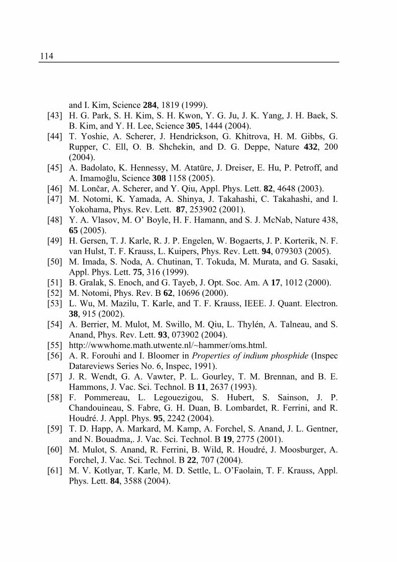
114
and I. Kim, Science 284, 1819 (1999).
[43] H. G. Park, S. H. Kim, S. H. Kwon, Y. G. Ju, J. K. Yang, J. H. Baek, S. B. Kim, and Y. H. Lee, Science 305, 1444 (2004).
[44] T. Yoshie, A. Scherer, J. Hendrickson, G. Khitrova, H. M. Gibbs, G. Rupper, C. Ell, O. B. Shchekin, and D. G. Deppe, Nature 432, 200 (2004).
[45] A. Badolato, K. Hennessy, M. Atatüre, J. Dreiser, E. Hu, P. Petroff, and A. Imamoğlu, Science 308 1158 (2005).
[46] M. Lončar, A. Scherer, and Y. Qiu, Appl. Phys. Lett. 82, 4648 (2003). [47] M. Notomi, K. Yamada, A. Shinya, J. Takahashi, C. Takahashi, and I.
Yokohama, Phys. Rev. Lett. 87, 253902 (2001). [48] Y. A. Vlasov, M. O’ Boyle, H. F. Hamann, and S. J. McNab, Nature 438,
65 (2005). [49] H. Gersen, T. J. Karle, R. J. P. Engelen, W. Bogaerts, J. P. Korterik, N. F.
van Hulst, T. F. Krauss, L. Kuipers, Phys. Rev. Lett. 94, 079303 (2005). [50] M. Imada, S. Noda, A. Chutinan, T. Tokuda, M. Murata, and G. Sasaki,
Appl. Phys. Lett. 75, 316 (1999). [51] B. Gralak, S. Enoch, and G. Tayeb, J. Opt. Soc. Am. A 17, 1012 (2000). [52] M. Notomi, Phys. Rev. B 62, 10696 (2000). [53] L. Wu, M. Mazilu, T. Karle, and T. F. Krauss, IEEE. J. Quant. Electron.
38, 915 (2002). [54] A. Berrier, M. Mulot, M. Swillo, M. Qiu, L. Thylén, A. Talneau, and S.
Anand, Phys. Rev. Lett. 93, 073902 (2004). [55] http://wwwhome.math.utwente.nl/~hammer/oms.html. [56] A. R. Forouhi and I. Bloomer in Properties of indium phosphide (Inspec
Datareviews Series No. 6, Inspec, 1991). [57] J. R. Wendt, G. A. Vawter, P. L. Gourley, T. M. Brennan, and B. E.
Hammons, J. Vac. Sci. Technol. B 11, 2637 (1993). [58] F. Pommereau, L. Legouezigou, S. Hubert, S. Sainson, J. P.
Chandouineau, S. Fabre, G. H. Duan, B. Lombardet, R. Ferrini, and R. Houdré. J. Appl. Phys. 95, 2242 (2004).
[59] T. D. Happ, A. Markard, M. Kamp, A. Forchel, S. Anand, J. L. Gentner, and N. Bouadma,. J. Vac. Sci. Technol. B 19, 2775 (2001).
[60] M. Mulot, S. Anand, R. Ferrini, B. Wild, R. Houdré, J. Moosburger, A. Forchel, J. Vac. Sci. Technol. B 22, 707 (2004).
[61] M. V. Kotlyar, T. Karle, M. D. Settle, L. O’Faolain, T. F. Krauss, Appl. Phys. Lett. 84, 3588 (2004).
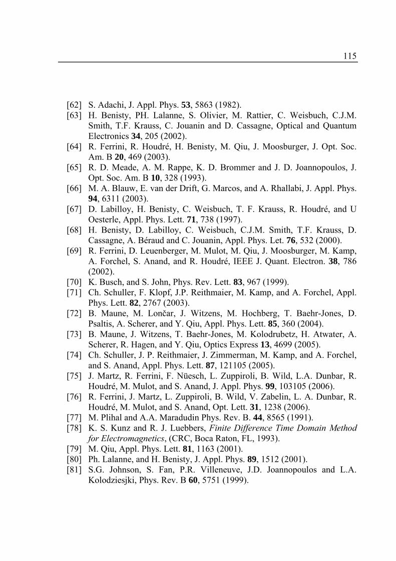
115
[62] S. Adachi, J. Appl. Phys. 53, 5863 (1982). [63] H. Benisty, PH. Lalanne, S. Olivier, M. Rattier, C. Weisbuch, C.J.M.
Smith, T.F. Krauss, C. Jouanin and D. Cassagne, Optical and Quantum Electronics 34, 205 (2002).
[64] R. Ferrini, R. Houdré, H. Benisty, M. Qiu, J. Moosburger, J. Opt. Soc. Am. B 20, 469 (2003).
[65] R. D. Meade, A. M. Rappe, K. D. Brommer and J. D. Joannopoulos, J. Opt. Soc. Am. B 10, 328 (1993).
[66] M. A. Blauw, E. van der Drift, G. Marcos, and A. Rhallabi, J. Appl. Phys. 94, 6311 (2003).
[67] D. Labilloy, H. Benisty, C. Weisbuch, T. F. Krauss, R. Houdré, and U Oesterle, Appl. Phys. Lett. 71, 738 (1997).
[68] H. Benisty, D. Labilloy, C. Weisbuch, C.J.M. Smith, T.F. Krauss, D. Cassagne, A. Béraud and C. Jouanin, Appl. Phys. Let. 76, 532 (2000).
[69] R. Ferrini, D. Leuenberger, M. Mulot, M. Qiu, J. Moosburger, M. Kamp, A. Forchel, S. Anand, and R. Houdré, IEEE J. Quant. Electron. 38, 786 (2002).
[70] K. Busch, and S. John, Phys. Rev. Lett. 83, 967 (1999). [71] Ch. Schuller, F. Klopf, J.P. Reithmaier, M. Kamp, and A. Forchel, Appl.
Phys. Lett. 82, 2767 (2003). [72] B. Maune, M. Lončar, J. Witzens, M. Hochberg, T. Baehr-Jones, D.
Psaltis, A. Scherer, and Y. Qiu, Appl. Phys. Lett. 85, 360 (2004). [73] B. Maune, J. Witzens, T. Baehr-Jones, M. Kolodrubetz, H. Atwater, A.
Scherer, R. Hagen, and Y. Qiu, Optics Express 13, 4699 (2005). [74] Ch. Schuller, J. P. Reithmaier, J. Zimmerman, M. Kamp, and A. Forchel,
and S. Anand, Appl. Phys. Lett. 87, 121105 (2005). [75] J. Martz, R. Ferrini, F. Nüesch, L. Zuppiroli, B. Wild, L.A. Dunbar, R.
Houdré, M. Mulot, and S. Anand, J. Appl. Phys. 99, 103105 (2006). [76] R. Ferrini, J. Martz, L. Zuppiroli, B. Wild, V. Zabelin, L. A. Dunbar, R.
Houdré, M. Mulot, and S. Anand, Opt. Lett. 31, 1238 (2006). [77] M. Plihal and A.A. Maradudin Phys. Rev. B. 44, 8565 (1991). [78] K. S. Kunz and R. J. Luebbers, Finite Difference Time Domain Method
for Electromagnetics, (CRC, Boca Raton, FL, 1993). [79] M. Qiu, Appl. Phys. Lett. 81, 1163 (2001). [80] Ph. Lalanne, and H. Benisty, J. Appl. Phys. 89, 1512 (2001). [81] S.G. Johnson, S. Fan, P.R. Villeneuve, J.D. Joannopoulos and L.A.
Kolodziesjki, Phys. Rev. B 60, 5751 (1999).
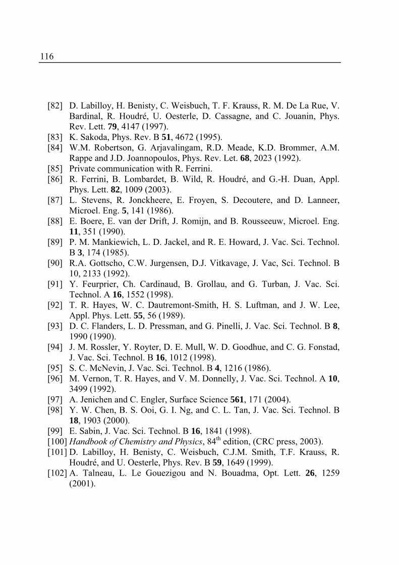
116
[82] D. Labilloy, H. Benisty, C. Weisbuch, T. F. Krauss, R. M. De La Rue, V.
Bardinal, R. Houdré, U. Oesterle, D. Cassagne, and C. Jouanin, Phys. Rev. Lett. 79, 4147 (1997).
[83] K. Sakoda, Phys. Rev. B 51, 4672 (1995). [84] W.M. Robertson, G. Arjavalingam, R.D. Meade, K.D. Brommer, A.M.
Rappe and J.D. Joannopoulos, Phys. Rev. Let. 68, 2023 (1992). [85] Private communication with R. Ferrini. [86] R. Ferrini, B. Lombardet, B. Wild, R. Houdré, and G.-H. Duan, Appl.
Phys. Lett. 82, 1009 (2003). [87] L. Stevens, R. Jonckheere, E. Froyen, S. Decoutere, and D. Lanneer,
Microel. Eng. 5, 141 (1986). [88] E. Boere, E. van der Drift, J. Romijn, and B. Rousseeuw, Microel. Eng.
11, 351 (1990). [89] P. M. Mankiewich, L. D. Jackel, and R. E. Howard, J. Vac. Sci. Technol.
B 3, 174 (1985). [90] R.A. Gottscho, C.W. Jurgensen, D.J. Vitkavage, J. Vac, Sci. Technol. B
10, 2133 (1992). [91] Y. Feurprier, Ch. Cardinaud, B. Grollau, and G. Turban, J. Vac. Sci.
Technol. A 16, 1552 (1998). [92] T. R. Hayes, W. C. Dautremont-Smith, H. S. Luftman, and J. W. Lee,
Appl. Phys. Lett. 55, 56 (1989). [93] D. C. Flanders, L. D. Pressman, and G. Pinelli, J. Vac. Sci. Technol. B 8,
1990 (1990). [94] J. M. Rossler, Y. Royter, D. E. Mull, W. D. Goodhue, and C. G. Fonstad,
J. Vac. Sci. Technol. B 16, 1012 (1998). [95] S. C. McNevin, J. Vac. Sci. Technol. B 4, 1216 (1986). [96] M. Vernon, T. R. Hayes, and V. M. Donnelly, J. Vac. Sci. Technol. A 10,
3499 (1992). [97] A. Jenichen and C. Engler, Surface Science 561, 171 (2004). [98] Y. W. Chen, B. S. Ooi, G. I. Ng, and C. L. Tan, J. Vac. Sci. Technol. B
18, 1903 (2000). [99] E. Sabin, J. Vac. Sci. Technol. B 16, 1841 (1998). [100] Handbook of Chemistry and Physics, 84th edition, (CRC press, 2003). [101] D. Labilloy, H. Benisty, C. Weisbuch, C.J.M. Smith, T.F. Krauss, R.
Houdré, and U. Oesterle, Phys. Rev. B 59, 1649 (1999). [102] A. Talneau, L. Le Gouezigou and N. Bouadma, Opt. Lett. 26, 1259
(2001).
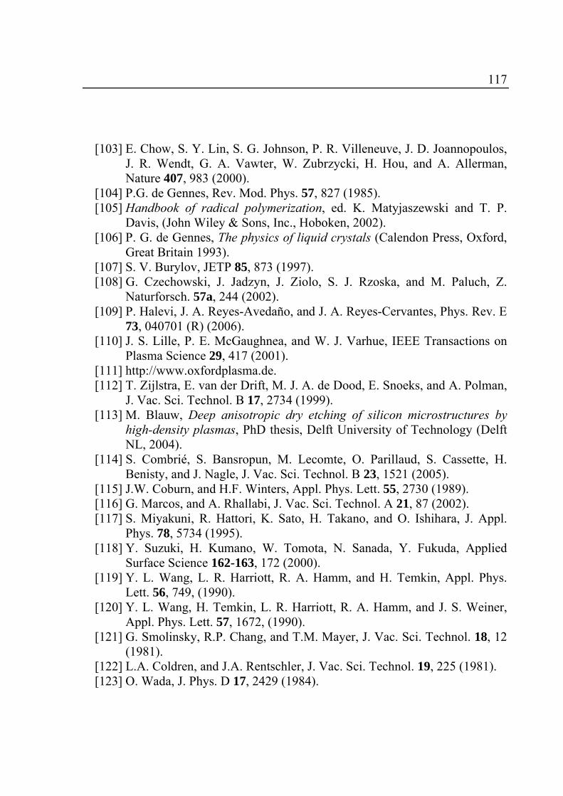
117
[103] E. Chow, S. Y. Lin, S. G. Johnson, P. R. Villeneuve, J. D. Joannopoulos,
J. R. Wendt, G. A. Vawter, W. Zubrzycki, H. Hou, and A. Allerman, Nature 407, 983 (2000).
[104] P.G. de Gennes, Rev. Mod. Phys. 57, 827 (1985). [105] Handbook of radical polymerization, ed. K. Matyjaszewski and T. P.
Davis, (John Wiley & Sons, Inc., Hoboken, 2002). [106] P. G. de Gennes, The physics of liquid crystals (Calendon Press, Oxford,
Great Britain 1993). [107] S. V. Burylov, JETP 85, 873 (1997). [108] G. Czechowski, J. Jadzyn, J. Ziolo, S. J. Rzoska, and M. Paluch, Z.
Naturforsch. 57a, 244 (2002). [109] P. Halevi, J. A. Reyes-Avedaño, and J. A. Reyes-Cervantes, Phys. Rev. E
73, 040701 (R) (2006). [110] J. S. Lille, P. E. McGaughnea, and W. J. Varhue, IEEE Transactions on
Plasma Science 29, 417 (2001). [111] http://www.oxfordplasma.de. [112] T. Zijlstra, E. van der Drift, M. J. A. de Dood, E. Snoeks, and A. Polman,
J. Vac. Sci. Technol. B 17, 2734 (1999). [113] M. Blauw, Deep anisotropic dry etching of silicon microstructures by
high-density plasmas, PhD thesis, Delft University of Technology (Delft NL, 2004).
[114] S. Combrié, S. Bansropun, M. Lecomte, O. Parillaud, S. Cassette, H. Benisty, and J. Nagle, J. Vac. Sci. Technol. B 23, 1521 (2005).
[115] J.W. Coburn, and H.F. Winters, Appl. Phys. Lett. 55, 2730 (1989). [116] G. Marcos, and A. Rhallabi, J. Vac. Sci. Technol. A 21, 87 (2002). [117] S. Miyakuni, R. Hattori, K. Sato, H. Takano, and O. Ishihara, J. Appl.
Phys. 78, 5734 (1995). [118] Y. Suzuki, H. Kumano, W. Tomota, N. Sanada, Y. Fukuda, Applied
Surface Science 162-163, 172 (2000). [119] Y. L. Wang, L. R. Harriott, R. A. Hamm, and H. Temkin, Appl. Phys.
Lett. 56, 749, (1990). [120] Y. L. Wang, H. Temkin, L. R. Harriott, R. A. Hamm, and J. S. Weiner,
Appl. Phys. Lett. 57, 1672, (1990). [121] G. Smolinsky, R.P. Chang, and T.M. Mayer, J. Vac. Sci. Technol. 18, 12
(1981). [122] L.A. Coldren, and J.A. Rentschler, J. Vac. Sci. Technol. 19, 225 (1981). [123] O. Wada, J. Phys. D 17, 2429 (1984).
118
[124] R.H. Burton, and G. Smolinsky, J. Electrochem. Soc. 129, 1599 (1982). [125] C. Youtsey, R. Grundbacher, R. Panepucci, I. Adesida, and C. Caneau, J.
Vac. Sci. Technol. B 12, 3317 (1994). [126] P. Strasser, R. Wüest, F. Robin, K. Rauscher, B. Wild, D. Erni, and H.
Jäckel, Proc. 17th Indium Phosphide and Related Materials Conference, Glasgow, Ireland (2005).
[127] C. Liguda, G. Böttger, A. Kuligk, R. Blum, M. Eich, H. Roth, J. Kunert, W. Morgenroth, H. Elsner, and H. G. Meyer, Appl. Phys. Lett. 78, 2434 (2001).
[128] W. Bogaerts, D. Taillaert, B. Luyssaert, P. Dumon, J. Van Campenhout, P. Bienstman, D. Van Thourhout, R. Baets, V. Wiaux, and S. Beckx, Opt. Express 12, 1583 (2004).
[129] N. Fukaya, D. Ohsaki, and T. Baba, Jpn. J. Appl Phys. 39, 2619 (2000). [130] S. I. Bozhevolnyi and L. Kuipers, Semicond. Sci. Technol. 21, R1 (2006). [131] M. L. M. Balistreri, J. P. Korterik, L. Kuipers, N. F. van Hulst, Phys.
Rev. Lett. 85, 294 (2000). [132] M. L. M. Balistreri, H. Gersen, J. P. Korterik, L. Kuipers, N. F. van
Hulst, Science 294, 1080 (2001). [133] V. N. Astratov, D. M. Whittaker, I. S. Culshaw, R. M. Stevenson, M. S.
Skolnick, T. F. Krauss, and R. M. De La Rue, Phys. Rev. B 60, R16255 (1999).
[134] G. Tittelbach, B. Richter, and W. Karthe, Pure Appl. Opt. 2, 683 (1993). [135] Y. C. Zhu, F. Karouta, E. J. Geluk, T. de Vries, J. J. G. M. v.d. Tol, J. J.
M. Binsma, and M. K. Smit, Proc. Symposium IEEE/LEOS Benelux Chapter, Enschede, The Netherlands, 81 (2003). Available at: http://www.leosbenelux.org.
[136] R. Ferrini, A. Berrier, L. A. Dunbar, R. Houdré, M. Mulot, S. Anand, S. de Rossi, and A. Talneau, Appl. Phys. Lett. 85, 3998 (2004).
[137] S. Iwamoto, S. Ishida, Y. Arakawa, M. Tokushima, A. Gomyo, H. Yamada, A. Higo, H. Toshiyoshi, and H. Fujita, Appl. Phys. Lett. 88, 011104 (2006).
[138] S. Jun and Y. S. Cho, Opt. Express 11, 2769 (2003). [139] W. Park, J. B. Lee, Appl. Phys. Lett. 84, 4845 (2004). [140] I. Märki, M. Salt, and H. P. Herzig, Opt. Express 7, 2970 (2006). [141] C. Kee, J. Kim, and H.Y. Park, Phys. Rev. B 61, 15523 (2000). [142] A. Figotin, and Y.A. Godin, Phys. Rev. B 57, 2841 (1998). [143] B. Wild, R. Ferrini, R. Houdré, M. Mulot, S. Anand, and C.J.M. Smith,
119
Appl. Phys. Lett. 84, 846 (2005).
[144] S. Gouza, C. H. Wen, S. T. Wu, N. Janarthanan, and C. S. Hsu, Jpn, J. Appl. Phys. 43 (Part 1), 7634 (2004).
[145] K. Busch, and S. John, Phys. Rev. Lett. 83, 967 (1999). [146] R. Ozaki, T. Matsui, M. Ozaki, and K. Yoshino, Appl. Phys.Lett. 82,
3593 (2003). [147] Y. K. Ha, Y. C. Yang, J. E. Kim, and H. Y. Park, Appl. Phys. Lett. 79, 15
(2001). [148] S. M. Weiss and P. M. Fauchet, Phys. Stat. Sol. a 197, 556 (2003). [149] S. M. Weiss, H. Ouyang, J. Zhang, and P. M. Fauchet, Opt. Express 13,
1090 (2005). [150] S. W. Leonard, J. P. Mondia, H. M. van Driel, O. Toader, S. John, K.
Busch, A. Birner, U. Gösele, and V. Lehmann, Phys. Rev. B 61, R2389 (2000).
[151] G. Mertens, T. Röder, H. Matthias, H. Marsmann, H.S.R. Kitzerow, S. Schweizer, C. Jamois, R.B. Wehrspohn, and M. Neubert, Appl. Phys. Lett. 83, 3036 (2003).
[152] M. Haurylau, S. P. Anderson, K. L. Marshall, and P. M. Fauchet, Appl. Phys. Lett. 88, 061103 (2006).
[153] M. Haurylau, A. R. Schroff, and P. M. Fauchet, Phys. Stat. Sol. a 202, 1477 (2005).
[154] N. Susa, Jpn. J. Appl. Phys. (Part 1) 39, 3466 (2000). [155] S. Gottardo, D.S. Wiersma, and W.V. Vos, Physica B 338, 143 (2003). [156] H. Takeda and K. Yoshino, Phys. Rev. B 67, 073106 (2003). [157] T. Yasuda, Y. Tsuji, and M. Koshiba, IEEE Photon. Technol. Lett. 17, 55
(2005). [158] G. Alagappan, X. W. Sun, M. B. Yu, P. Shum, and D. den Engelsen,
IEEE J. Quant. Electr. 42, 404 (2006). [159] G. Alagappan, X. W. Sun, P. Shum, and M. B. Yu, Opt. Lett. 31, 1109
(2006). [160] A. E. Miroshnichenko, I. Pinkevych, and Y. S. Kivshar, Opt. Express 14,
2839 (2006). [161] A. Clark, and S. T. Lagerwall, Appl. Phys. Lett. 36, 899 (1980). [162] Polymers for Photonics Applications II in Advances in Polymer Science,
Vol. 161, Ed. K.S. Lee (Springer-Verlag, Heidelberg, 2003). [163] M.B. Flynn, L. O’Faolain, and T.F. Krauss, J. Opt. Soc. Am. B 22, 792
(2005).

120
[164] M.M. Raj, S. Toyoshima, and S. Arai, Jpn. J. Appl. Phys 38, L811
(1999). [165] S. Mingaleev, M. Schillinger, D. Hermann, and K. Busch, Opt. Lett. 29,
2858 (2004). [166] Y. Jiao, M. Schillinger, D. A. B. Miller, S. Fan, and K. Busch, IEEE
Photon. Technol. Lett. 17, 1875 (2005). [167] K. Nielsen, D. Noordegraaf, T. Sørensen, A Bjarklev and T. P. Hansen, J.
Opt. A: Pure Appl. Opt. 7, L13 (2005). [168] A.F. Stancell, chapter 12 of Polymer Science and Materials, ed. A.V.
Tobolsky, and H.F. Mark (Wiley-Interscience, 1971). [169] J. Martz, L. Zuppiroli, and F. Nüesch, Langmuir 20, 11428 (2004). [170] P. G. de Gennes, Rev. Mod. Phys. 57, 827 (1985). [171] Private communication with S. Cheylan.


![Photonic Integration With Epitaxial III–V on Silicon...can be found in [3], and an excellent overview of Si3N4 versus SOI can be found in [5]. B. InP Photonic integration on InP,](https://img.pdfslide.us/doc/110x75/5ee10731ad6a402d666c0f57/photonic-integration-with-epitaxial-iiiav-on-silicon-can-be-found-in-3.jpg)