Embed Size (px)
Citation preview
University of Central Florida University of Central Florida
STARS STARS
Electronic Theses and Dissertations, 2004-2019
2011
Study Of Esd Effects On Rf Power Amplifiers Study Of Esd Effects On Rf Power Amplifiers
Raju, Divya Narasimha University of Central Florida
Part of the Electrical and Electronics Commons
Find similar works at: https://stars.library.ucf.edu/etd
University of Central Florida Libraries http://library.ucf.edu
This Masters Thesis (Open Access) is brought to you for free and open access by STARS. It has been accepted for
inclusion in Electronic Theses and Dissertations, 2004-2019 by an authorized administrator of STARS. For more
information, please contact [email protected].
STARS Citation STARS Citation Narasimha, Raju, Divya, "Study Of Esd Effects On Rf Power Amplifiers" (2011). Electronic Theses and Dissertations, 2004-2019. 2088. https://stars.library.ucf.edu/etd/2088
STUDY OF ESD EFFECTS ON RF POWER AMPLIFIERS
by
DIVYA NARASIMHA RAJU
B.S. Visvesvaraya Technological University, 2006
A thesis submitted in partial fulfillment of the requirements
for the degree of Master of Science
in the Department of Electrical Engineering and Computer Science
in the College of Engineering and Computer Science
at the University of Central Florida
Orlando, Florida
Spring Term
2011

ii
© 2011 Divya Narasimha Raju
iii
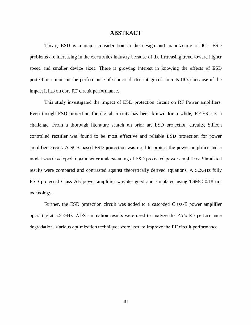
ABSTRACT
Today, ESD is a major consideration in the design and manufacture of ICs. ESD
problems are increasing in the electronics industry because of the increasing trend toward higher
speed and smaller device sizes. There is growing interest in knowing the effects of ESD
protection circuit on the performance of semiconductor integrated circuits (ICs) because of the
impact it has on core RF circuit performance.
This study investigated the impact of ESD protection circuit on RF Power amplifiers.
Even though ESD protection for digital circuits has been known for a while, RF-ESD is a
challenge. From a thorough literature search on prior art ESD protection circuits, Silicon
controlled rectifier was found to be most effective and reliable ESD protection for power
amplifier circuit. A SCR based ESD protection was used to protect the power amplifier and a
model was developed to gain better understanding of ESD protected power amplifiers. Simulated
results were compared and contrasted against theoretically derived equations. A 5.2GHz fully
ESD protected Class AB power amplifier was designed and simulated using TSMC 0.18 um
technology.
Further, the ESD protection circuit was added to a cascoded Class-E power amplifier
operating at 5.2 GHz. ADS simulation results were used to analyze the PA’s RF performance
degradation. Various optimization techniques were used to improve the RF circuit performance.

iv
Dedicated to My Father
v
ACKNOWLEDGMENTS
I would like to thank my advisor, Dr. Jiann S. Yuan, for his continuous commitment to
help and support me through my graduate career. I wish to express my sincerest gratitude to him
for providing me with timely guidance as well as the moral support and encouragement in the
research work. I am also thankful to Dr. Kalpathy Sundaram and Dr. Lee Chow for serving on
my committee.
I would also like to extend my thanks to my dear colleagues Karan Kutty, Shuyu Chen,
Yiheng Wang, Giji Skaria, Jason Steighner for their invaluable help during my research work. A
special thanks to Qiang cui for his valuable contribution that improved my work significantly.
My heartfelt thanks go out to my beloved mother Sarala, my brother Mukund and dear
friend Kiran for their constant support and Encouragement.
Finally, a special mention must be made to express my deepest gratitude to my husband
Narasimha Nagaiah, who supported me with his love for every moment during ups and downs of
this work.
vi
TABLE OF CONTENTS
LIST OF FIGURES ..................................................................................................................... viii
LIST OF TABLES .......................................................................................................................... x
LIST OF ACRONYMS AND ABBREVIATIONS ...................................................................... xi
CHAPTER ONE: INTRODUCTION ............................................................................................. 1
Need for ESD .............................................................................................................................. 1
RF-ESD ....................................................................................................................................... 2
Motivation ................................................................................................................................... 4
Goals and Outline ....................................................................................................................... 5
References ................................................................................................................................... 6
CHAPTER TWO: ELECTROSTATIC DISCHARGE .................................................................. 7
ESD Induced Failures ................................................................................................................. 8
ESD Test Models ...................................................................................................................... 10
ESD Protection Circuits ............................................................................................................ 12
CHAPTER THREE: SCR BASED ESD PROTECTION ............................................................ 15
ESD Protection Devices ............................................................................................................ 15
ESD Design Window ........................................................................................................... 16
Prior Art ESD Protection Devices ........................................................................................ 17
Why SCR? ............................................................................................................................ 18
Implementation of On-Chip ESD Protection ............................................................................ 19
I/O Pad ESD Protection ........................................................................................................ 23
Power Supply Clamp ............................................................................................................ 24
ESD Parasitics Modeling .......................................................................................................... 25
vii
References ................................................................................................................................. 28
CHAPTER FOUR: ESD PROTECTED POWER AMPLIFIERS................................................ 29
Modeling of Class-A Power Amplifier with ESD .................................................................... 31
Class-AB Power Amplifier with Full ESD protection .............................................................. 35
Simulation Results ................................................................................................................ 37
ESD Protected Class-E Power Amplifier ................................................................................. 40
Simulation Results ................................................................................................................ 44
References ................................................................................................................................. 45
CHAPTER FIVE: CONCLUSION............................................................................................... 46
CHAPTER SIX: FUTURE WORK .............................................................................................. 47
viii
LIST OF FIGURES
Figure 1.1: General overview of a transceiver circuit..................................................................... 2
Figure 1.2: RF-ESD design flow .................................................................................................... 4
Figure 2.1: Human body model circuit and corresponding waveform ......................................... 10
Figure 2.2: Machine Model circuit and corresponding waveform ............................................... 11
Figure 2.3: Charged Device Model circuit and corresponding waveform.................................... 12
Figure 2.4: (a) Low-C, (b) Impedance Cancellation and (c) Impedance Isolation based ESD
protection ...................................................................................................................................... 13
Figure 3.1: ESD design window ................................................................................................... 16
Figure 3.2: Basic structure of SCR and its equivalent circuit ....................................................... 18
Figure 3.3: ESD zapping modes (a) PS-mode, (b) NS-mode, (c) PD-mode and (d) ND-mode ... 21
Figure 3.4: Schematic Diagram of ESD protection for RF power amplifier ................................ 22
Figure 3.5: Cross-sectional view of MLSCR ................................................................................ 24
Figure 3.6: Cross-sectional view of HHSCR ................................................................................ 25
Figure 3.7: RC modeling of SCR device parasitics ...................................................................... 26
Figure 4.1: (a) Class-A power amplifier circuit, (b) Class-A PA with ESD protection circuit .... 31
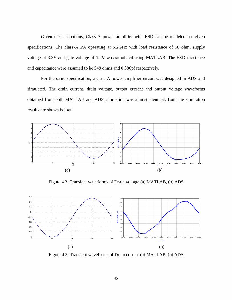
Figure 4.2: Transient waveforms of Drain voltage (a) MATLAB, (b) ADS ................................ 33
Figure 4.3: Transient waveforms of Drain current (a) MATLAB, (b) ADS ................................ 33
Figure 4.4: Transient waveforms of Output voltage (a) MATLAB, (b) ADS .............................. 34
Figure 4.5: Transient waveforms of Output current (a) MATLAB, (b) ADS .............................. 34
Figure 4.6: Transient waveforms of ESD Capacitance current (a) MATLAB, (b) ADS ............. 34
Figure 4.7: Complete circuit diagram of fully ESD protected Class-AB PA. .............................. 35
ix
Figure 4.8: Layout view of Class-AB PA with ESD protection. .................................................. 36
Figure 4.9: Gain and Output Power (a) Without ESD and (b) With ESD protection ................... 37
Figure 4.10: PAE (a) Without ESD and (b) With ESD protection ............................................... 37
Figure 4.11: Stability Factor (a) Without ESD and (b) With ESD protection .............................. 38
Figure 4.12: S21 (a) Without ESD and (b) With ESD protection ................................................ 38
Figure 4.13: S11 (a) Without ESD and (b) With ESD protection ................................................ 39
Figure 4.14: Basic Class-E power amplifier circuit ...................................................................... 41
Figure 4.15: ESD protected Class-E power Amplifier Circuit Diagram ...................................... 42
Figure 4.16: Effect of gate voltage on ESD protected class-E PA performance .......................... 43
Figure 4.17: Effect of load capacitance on ESD protected class-E PA performance ................... 44
x
LIST OF TABLES
Table 2.1: Example of Static Charge Generation ........................................................................... 8
Table 2.2: Sensitivity of Electronic Devices to Damage by ESD................................................... 8
Table 2.3: Comparison of ESD test models and parasitic components ........................................ 12
Table 3.1: Calculated parasitic Resistance and Capacitance values of RC model ....................... 27
Table 3.2: Comparison of S-parameters obtained from SCR device simulation and ADS
simulation of RC model ................................................................................................................ 27
Table 4.1: Comparison of RF circuit performance with and without ESD protection in this work
and reference [4] ........................................................................................................................... 40
Table 4.2: Comparison of RF performance of Class-E PA, before and after optimization. ......... 44
xi
LIST OF ACRONYMS AND ABBREVIATIONS
ADC Analog-to-Digital Converter
ADS Advanced Design System
CDM Charged Device Model
CMOS Complementary Metal Oxide Semiconductor
DAC Digital-to-Analog Converter
DE Drain Efficiency
ESD Electrostatic Discharge
GGNMOS Gate Grounded NMOS
HBM Human Body Model
HHSCR High Holding voltage SCR
IC Integrated Circuit
KVL Kirchhoff's Voltage Law
LNA Low-noise Amplifier
MM Machine Model
MLSCR Modified Lateral SCR
MOSFET Metal-Oxide Semiconductor Field Effect Transistor
NMOS n-Channel Metal Oxide Semiconductor
PA Power Amplifier
PAE Power Added Efficiency
RF Radio Frequency
RH Relative Humidity
SCR Silicon Controlled Rectifier

xii
TSMC Taiwan Semiconductor Manufacturing Company
1
CHAPTER ONE: INTRODUCTION
Wireless communication revolution is at its peak like never before and is evident from
the fast, compact and affordable smart phones available in market today. The growing
dependency on these devices has increased reliability concerns and thus constant effort has been
put to ensure all products are highly reliable and can withstand severe electrostatic discharges.
With the increasing speed and decreasing size of devices, there will always be new ESD related
concerns rising and more challenges to be faced.
Need for ESD
ESD has become the primary reliability concern in modern integrated circuits(IC). An IC
can be subjected to ESD zapping at various places, right from fabrication room to end-user.
Especially, thinner gate oxides and shallower diffusion junction increase the risk of ESD
damage. A 1999 study estimates that up to 30% of all CMOS failures can be attributed to ESD
damage and that ESD related damage has cost the IC industry billions of dollars [1], thus ESD
related concerns can no longer be ignored. Precautions have been taken to avoid any electrostatic
discharge during manufacturing process. However, for an IC to be reliable, it should be able to
handle the ESD stress at any point. Therefore, incorporation of ESD protection circuit in the
semiconductor chip is vital. The main focus is to identify the ESD susceptible devices and
protect them. Designers should also test and characterize their circuits to ensure that the IC’s are
immune to severe ESD events.
2
RF-ESD
ESD protection circuits have been intensely researched for a while now, especially for
Digital IC’s. Research shows that very reliable ESD protection circuits are available for Digital
IC’s like high speed interface circuits. As and when integration of RF circuits into CMOS IC’s
became familiar, an interesting yet very challenging field of research called “RF-ESD” was
introduced. Even though ESD protection circuit design was well known, RF-ESD has its own
concerns due to fact that addition of ESD protection circuit degrades RF circuit performance
significantly. Shown in Figure 1.1 is transceiver block diagram and it indicates that the two
blocks highly susceptible to ESD events are LNA and PA and hence needs to be protected.
Figure 1.1: General overview of a transceiver circuit
ESD protection circuit design principle for RF circuits is different from that of digital
circuitry. Figure 1.2 shows the RF-ESD circuit design flow. Some of the key concepts to be kept
in mind while designing RF-ESD are as follows. Firstly, the protection circuit for RF-ESD may
be a function of the application frequency. Below 1 GHz, a conventional digital ESD protection
BASEBAND
MODULE
DACFILTER
FILTER ADCFILTER
PA
LNA
ESD
ESD
LOCAL
OSCILLATOR
3
circuit can be used. Whereas, between 1GHz to 5 GHz, ESD versus RF optimization is required
and for 5GHz to 15GHz, RF-ESD co-design becomes mandatory. Secondly, Unlike in Digital
applications where the primary focus is on dc voltage shift and leakage, RF-ESD focuses on RF
circuit performance degradation. For example, when diode is used ESD protection in digital
circuits, the primary concern is differential voltage isolation whereas in case of RF-ESD, it will
be capacitive coupling and stability. Lastly, the distinction between RF-ESD design and Digital
ESD design is circuit failure evaluation. In digital ESD, dc leakage alone determines failure
criteria whereas RF-ESD requires evaluation of many parameters like RF parameters, dc
parameters and system level requirements [2].
4
Figure 1.2: RF-ESD design flow
Motivation
Development of high speed, high performance RF circuits make it highly sensitive and
susceptible to ESD stress, also due to downscaling of CMOS technology. This makes ESD
protection circuit most integral part of design and manufacture of reliable IC’s. In spite of
5
researching ESD protection circuits for a longtime, it is a continuous struggle to find optimum
solution which will have zero impact on RF core circuits. In an effort to achieve this, we have
designed an ESD protected power amplifiers which will be explained in detail in the following
chapters. Optimization of the circuit will aid in improving circuit performance, however
implementing an effective ESD protection without disturbing the core RF circuit performance is
nearly impossible for now.
Goals and Outline
The ultimate goal of this research is to study the impact of ESD protection circuit on the
RF power amplifiers by modeling, simulating and finally optimizing to reduce the performance
degradation. Designs are simulated and verified using MATLAB and ADS tools.
The Introduction in Chapter One has presented the importance of RF-ESD and key
concerns associated with RF-ESD. In Chapter Two, the fundamental of ESD and test models
such as HBM, MM are explained in brief. Chapter Three details the available device level
solution for ESD protection. Further, it will introduce the Modified Lateral SCR and High
Holding voltage SCR, the two devices used for ESD protection of RF power amplifiers as part of
this thesis, along with the reason why the SCR is chosen for ESD protection. Chapter Four will
discuss the basics of power amplifier design and explain the model derivation of the partially
protected Class-A PA using the analytical understanding backed by fundamental equations
describing circuit behavior. It also covers the design and simulation of fully ESD protected Class
AB power amplifier. This chapter also includes ESD protection for Switch mode Class E PA and
its optimization. The thesis finally concludes with Chapter Five and Chapter Six discussing the
conclusion and future work respectively.
6
References
[1] Wang, Albert Z H. On-Chip ESD Protection for Integrated Circuits, an IC Design
Perspective. Norwell, MA: Kluwer Academic Publishers, 2002
[2] Voldman, Steven H. ESD: RF Technology and Circuits. New York: Wiley, 2006
7
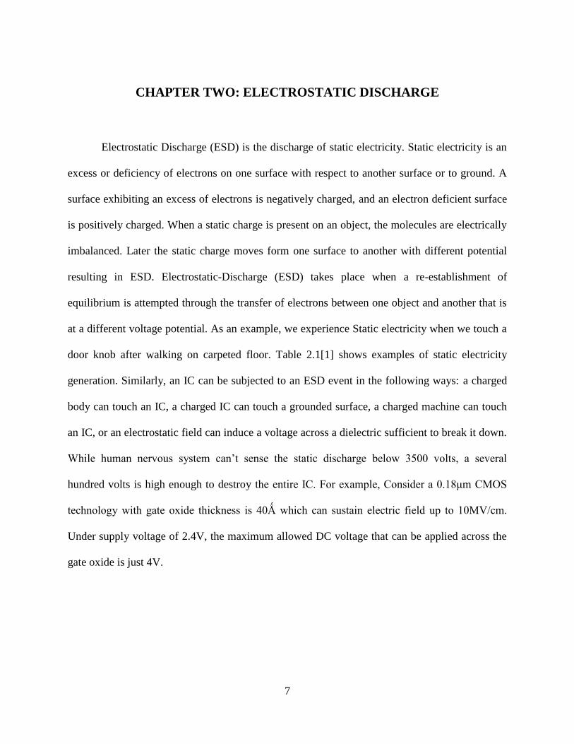
CHAPTER TWO: ELECTROSTATIC DISCHARGE
Electrostatic Discharge (ESD) is the discharge of static electricity. Static electricity is an
excess or deficiency of electrons on one surface with respect to another surface or to ground. A
surface exhibiting an excess of electrons is negatively charged, and an electron deficient surface
is positively charged. When a static charge is present on an object, the molecules are electrically
imbalanced. Later the static charge moves form one surface to another with different potential
resulting in ESD. Electrostatic-Discharge (ESD) takes place when a re-establishment of
equilibrium is attempted through the transfer of electrons between one object and another that is
at a different voltage potential. As an example, we experience Static electricity when we touch a
door knob after walking on carpeted floor. Table 2.1[1] shows examples of static electricity
generation. Similarly, an IC can be subjected to an ESD event in the following ways: a charged
body can touch an IC, a charged IC can touch a grounded surface, a charged machine can touch
an IC, or an electrostatic field can induce a voltage across a dielectric sufficient to break it down.
While human nervous system can’t sense the static discharge below 3500 volts, a several
hundred volts is high enough to destroy the entire IC. For example, Consider a 0.18μm CMOS
technology with gate oxide thickness is 40Ǻ which can sustain electric field up to 10MV/cm.
Under supply voltage of 2.4V, the maximum allowed DC voltage that can be applied across the
gate oxide is just 4V.
8
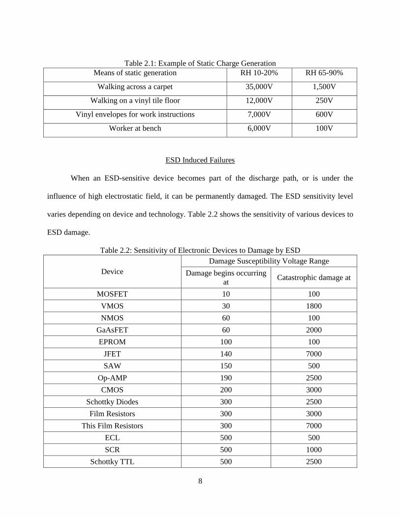
Table 2.1: Example of Static Charge Generation
Means of static generation RH 10-20% RH 65-90%
Walking across a carpet 35,000V 1,500V
Walking on a vinyl tile floor 12,000V 250V
Vinyl envelopes for work instructions 7,000V 600V
Worker at bench 6,000V 100V
ESD Induced Failures
When an ESD-sensitive device becomes part of the discharge path, or is under the
influence of high electrostatic field, it can be permanently damaged. The ESD sensitivity level
varies depending on device and technology. Table 2.2 shows the sensitivity of various devices to
ESD damage.
Table 2.2: Sensitivity of Electronic Devices to Damage by ESD
Device
Damage Susceptibility Voltage Range
Damage begins occurring
at Catastrophic damage at
MOSFET 10 100
VMOS 30 1800
NMOS 60 100
GaAsFET 60 2000
EPROM 100 100
JFET 140 7000
SAW 150 500
Op-AMP 190 2500
CMOS 200 3000
Schottky Diodes 300 2500
Film Resistors 300 3000
This Film Resistors 300 7000
ECL 500 500
SCR 500 1000
Schottky TTL 500 2500
9
Depending on how sensitive the device is, an ESD event can cause catastrophic/hard
failure or Latent/soft failure. Catastrophic failure is when the device stops functioning and has
been destroyed permanently. Where as in case of latent failure, the device seems to perform
normally but may not be reliable anymore. Some of ESD induced failures are:
1. Dielectric Breakdown: This is a predominant failure mechanism on MOS devices
when the voltage across the oxide exceeds the dielectric breakdown strength. This
failure mechanism is basically voltage dependent where the voltage must be high
enough to cause dielectric breakdown. As such, the thinner the oxide, the higher the
susceptibility to ESD.
2. Thermal Runaway (Second Breakdown): This failure mechanism results in junction
basically a power dependent failure mechanism; the ESD pulse shape, duration and
energy can produce power levels resulting in localized heating and eventually
junction melting, even though the voltage level is below that required to cause
dielectric breakdown.
3. Parametric Degradation: On precision, high speed ICs ESD can cause device
degradation, besides functional failures. This can impact electrical performance and
adversely affect device reliability. This degradation in device parametric performance
is far more difficult to pinpoint as an ESD related failure mode. It is also the least
understood among the failure modes. The extent of this degradation is dependent on
the number of ESD pulses and the level of damage sustained [2].
10
ESD Test Models
ESD can have serious detrimental effects on all semiconductor ICs and the system that
contains them. ESD events are by nature, unpredictable, a number of models have been
developed to characterize different ESD scenarios and events. These standard models help us to
enhance the quality and reliability of ICs by ensuring all devices employed have undergone
proper ESD design and testing, thereby minimizing the detrimental effects of ESD. Three major
test models are described below in detail.
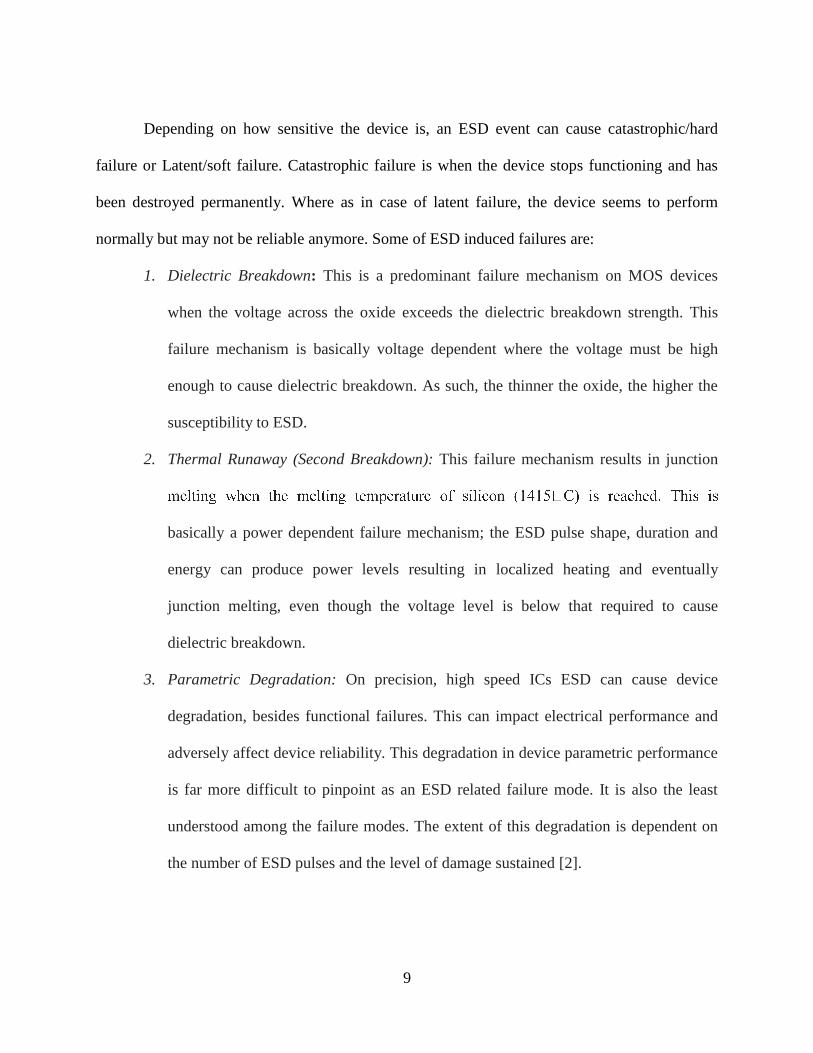
1. Human Body Model (HBM): This model represents the ESD event “Discharge to the
device”. In other words, when a charged human being touches the IC, there is direct
transfer of electrostatic charge from human body to the ESD sensitive device. The HBM
circuit model consists of capacitor which discharges through resistor and inductor. The
transient ESD pulse generated by this model has discharge current level of about 4A with
rise time of 10ns and discharge time of 150ns as shown in Figure 2.1.
Figure 2.1: Human body model circuit and corresponding waveform
VHBM
kV
RHBM
CHBM
LHBM
IC
11
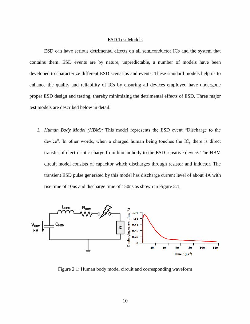
2. Machine Model (MM): Originated in Japan as a result of investigating worst-case
scenarios of the HBM, the Machine Model simulates the transient discharge of a charged
machine through the DUT and is represented by the lumped circuit shown in Figure
2.2. The MM is a damped sinusoidal oscillating current waveform, and the time to the
first current peak is typically 15ns with duration for the pulse of approximately 40ns.
Figure 2.2: Machine Model circuit and corresponding waveform
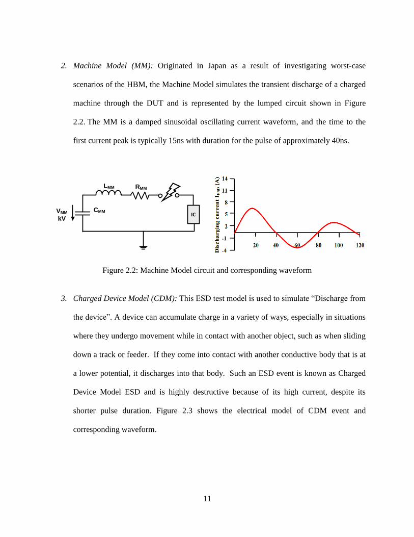
3. Charged Device Model (CDM): This ESD test model is used to simulate “Discharge from
the device”. A device can accumulate charge in a variety of ways, especially in situations
where they undergo movement while in contact with another object, such as when sliding
down a track or feeder. If they come into contact with another conductive body that is at
a lower potential, it discharges into that body. Such an ESD event is known as Charged
Device Model ESD and is highly destructive because of its high current, despite its
shorter pulse duration. Figure 2.3 shows the electrical model of CDM event and
corresponding waveform.
VMM
kV
RMM
CMM
LMM
IC
12
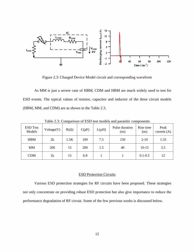
Figure 2.3: Charged Device Model circuit and corresponding waveform
As MM is just a severe case of HBM, CDM and HBM are much widely used to test for
ESD events. The typical values of resistor, capacitor and inductor of the three circuit models
(HBM, MM, and CDM) are as shown in the Table 2.3.
Table 2.3: Comparison of ESD test models and parasitic components
ESD Test
Models Voltage(V) R(Ω) C(pF) L(µH)
Pulse duration
(ns)
Rise time
(ns)
Peak
current (A)
HBM 2k 1.5K 100 7.5 150 2-10 1.33
MM 200 15 200 1.5 40 10-15 3.5
CDM 1k 15 6.8 1 1 0.1-0.5 12
ESD Protection Circuits
Various ESD protection strategies for RF circuits have been proposed. These strategies
not only concentrate on providing robust ESD protection but also give importance to reduce the
performance degradation of RF circuit. Some of the few previous works is discussed below.
RCDMLCDM
VCDM
kV
IC
CMM
ICDM
13
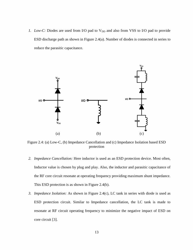
1. Low-C: Diodes are used from I/O pad to VDD and also from VSS to I/O pad to provide
ESD discharge path as shown in Figure 2.4(a). Number of diodes is connected in series to
reduce the parasitic capacitance.
(a) (b) (c)
Figure 2.4: (a) Low-C, (b) Impedance Cancellation and (c) Impedance Isolation based ESD
protection
2. Impedance Cancellation: Here inductor is used as an ESD protection device. Most often,
Inductor value is chosen by plug and play. Also, the inductor and parasitic capacitance of
the RF core circuit resonate at operating frequency providing maximum shunt impedance.
This ESD protection is as shown in Figure 2.4(b).
3. Impedance Isolation: As shown in Figure 2.4(c), LC tank in series with diode is used as
ESD protection circuit. Similar to Impedance cancellation, the LC tank is made to
resonate at RF circuit operating frequency to minimize the negative impact of ESD on
core circuit [3].
I/O
VDD
VSS
I/O I/O
VDD
14
References
[1] ESD Association. Fundamentals of Electrostatic Discharge-Part 1:An Introduction. August
2010, Rome, NY.
[2] Linear Technology. http://cds.linear.com/docs/quality/esdprotection.pdf. 2010.
[3] M.-D. Ker and Y.-W. Hsiao, “On-chip ESD protection strategies for RF circuits in CMOS
technology,” in Proceedings of the 8th International Conference on Solid-State and Integrated
Circuit Technology (ICSICT ’06), pp. 1680–1683.
[4] Amerasekera, Ajith and Duvvury, Charvaka. ESD in Silicon Integrated Circuits. West
Sussex: John Wiley & Sons, 2002.
15
CHAPTER THREE: SCR BASED ESD PROTECTION
Even though there are many ESD protection circuits readily available, ESD design
engineers face difficulty in finding a robust ESD protection circuit. Here, the main goal is not
only to achieve required level of protection but also minimize the impact it has on the core RFIC
performance. A conscious effort is needed to choose ESD protection unit with less parasitics,
smaller area and good ESD robustness. After intense study on various ESD protection devices
and circuits, Silicon controlled rectifier was found to be the promising candidate for ESD
protection of RF power amplifier. The following section defends why SCR was chosen and
further explains the on-chip ESD protection scheme in detail.
ESD Protection Devices
An ideal ESD protection device should be capable of providing a conductive path to
discharge the ESD current safely without disturbing the core circuit. The most important
properties an ideal ESD protection device must possess are described as follows. Firstly, the
device should be able to turn on instantaneously when ESD event occurs and should be in off
state during normal operation. It should also have zero resistance during ESD, in order to shunt
the ESD current as quickly as possible without any voltage drop. Secondly, in order to avoid the
unintentional triggering of the protection device, the sustaining voltage of the device must be
always greater than the supply voltage of the chip. Thirdly, the ideal device must be transparent
meaning should have no parasitics so that it will not interfere with core circuit performance.
Lastly, the ESD protection device must be reliable and should be capable of surviving the ESD
16
stress. It is also vital that the ESD protection device size is minimum, so that it does not increase
the overall chip area.
ESD Design Window
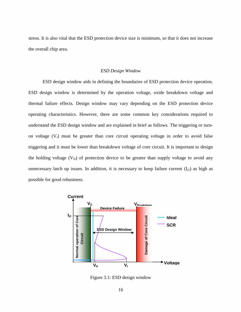
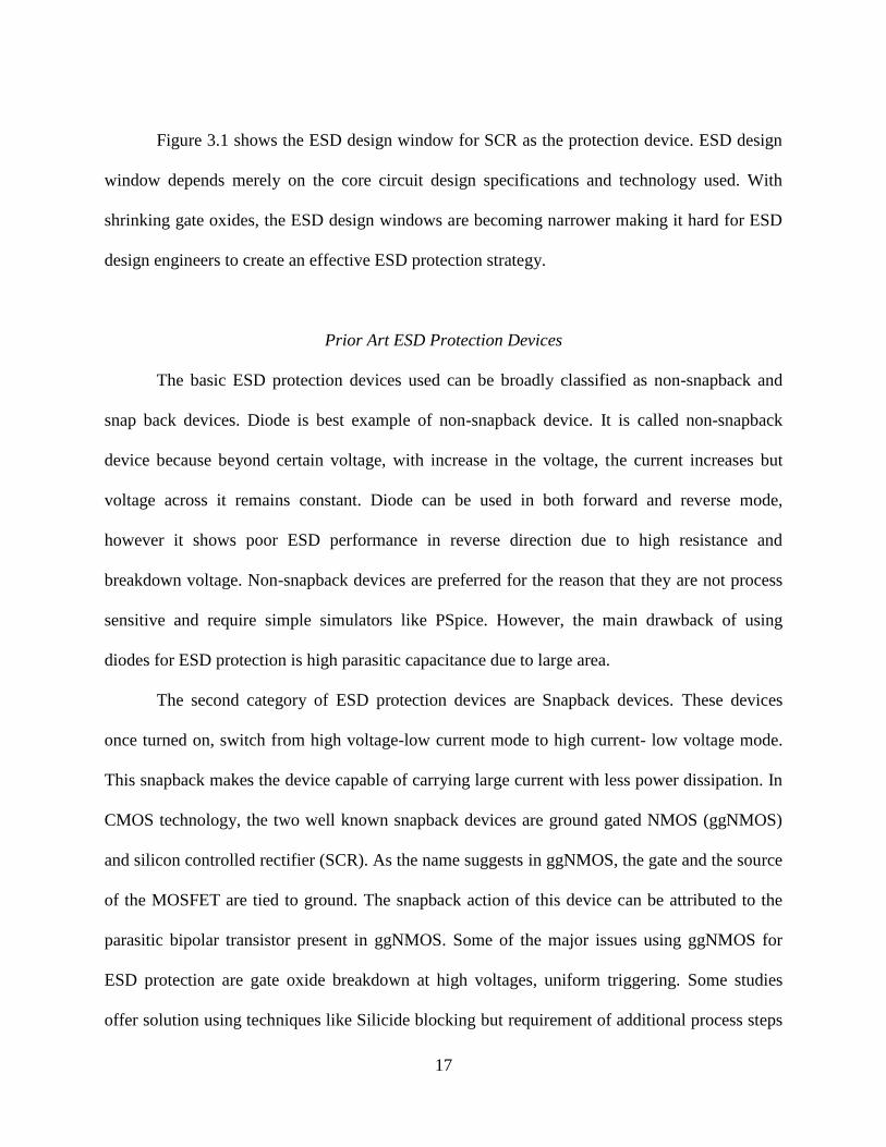
ESD design window aids in defining the boundaries of ESD protection device operation.
ESD design window is determined by the operation voltage, oxide breakdown voltage and
thermal failure effects. Design window may vary depending on the ESD protection device
operating characteristics. However, there are some common key considerations required to
understand the ESD design window and are explained in brief as follows. The triggering or turn-
on voltage (Vt) must be greater than core circuit operating voltage in order to avoid false
triggering and it must be lower than breakdown voltage of core circuit. It is important to design
the holding voltage (VH) of protection device to be greater than supply voltage to avoid any
unnecessary latch up issues. In addition, it is necessary to keep failure current (It2) as high as
possible for good robustness.
Figure 3.1: ESD design window
VD
D
VBreakdown
No
rma
l o
pe
rati
on
of
Co
re
C
ircu
it
Dam
ag
e o
f C
ore
Cir
cu
it
Current
Voltage VH Vt
ESD Design Window
It2
Device Failure
Ideal
SCR
17
Figure 3.1 shows the ESD design window for SCR as the protection device. ESD design
window depends merely on the core circuit design specifications and technology used. With
shrinking gate oxides, the ESD design windows are becoming narrower making it hard for ESD
design engineers to create an effective ESD protection strategy.
Prior Art ESD Protection Devices
The basic ESD protection devices used can be broadly classified as non-snapback and
snap back devices. Diode is best example of non-snapback device. It is called non-snapback
device because beyond certain voltage, with increase in the voltage, the current increases but
voltage across it remains constant. Diode can be used in both forward and reverse mode,
however it shows poor ESD performance in reverse direction due to high resistance and
breakdown voltage. Non-snapback devices are preferred for the reason that they are not process
sensitive and require simple simulators like PSpice. However, the main drawback of using
diodes for ESD protection is high parasitic capacitance due to large area.
The second category of ESD protection devices are Snapback devices. These devices
once turned on, switch from high voltage-low current mode to high current- low voltage mode.
This snapback makes the device capable of carrying large current with less power dissipation. In
CMOS technology, the two well known snapback devices are ground gated NMOS (ggNMOS)
and silicon controlled rectifier (SCR). As the name suggests in ggNMOS, the gate and the source
of the MOSFET are tied to ground. The snapback action of this device can be attributed to the
parasitic bipolar transistor present in ggNMOS. Some of the major issues using ggNMOS for
ESD protection are gate oxide breakdown at high voltages, uniform triggering. Some studies
offer solution using techniques like Silicide blocking but requirement of additional process steps
18
makes it expensive. SCR is another snapback device and has become the favorite choice among
ESD designers. While diode and ggNMOS are unidirectional devices (not ESD robust in reverse
direction), SCR can conduct ESD current efficiently in both directions. SCR is discussed in
detail in the following section, along with the reason why it has been chosen for ESD protection
of power amplifiers.
Why SCR?
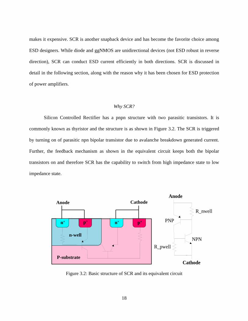
Silicon Controlled Rectifier has a pnpn structure with two parasitic transistors. It is
commonly known as thyristor and the structure is as shown in Figure 3.2. The SCR is triggered
by turning on of parasitic npn bipolar transistor due to avalanche breakdown generated current.
Further, the feedback mechanism as shown in the equivalent circuit keeps both the bipolar
transistors on and therefore SCR has the capability to switch from high impedance state to low
impedance state.
Figure 3.2: Basic structure of SCR and its equivalent circuit
P-substrate
n-well
n+ p+ n+ p+
Anode Cathode
Anode
Cathode
R_pwell
R_nwell
NPN
PNP
19
SCR can conduct very high current with very low on resistance mainly due to its almost
ideal conductivity modulation profile. SCR provides full voltage swing, meaning it can
efficiently discharge ESD current in both directions. In addition to it, it has low parasitic
capacitance, higher It2 and smaller area makes it a favorable choice for ESD protection.
However, it has some issues like the higher first breakdown voltage and lower holding voltage
(causes latch up) which has to be resolved. Literature search reveal various modified SCR’s
which tackle these shortcomings to some extent making SCR most preferred ESD protection
device.
There are few previous research papers which have presented ESD protection for power
amplifiers. Reference [1] and [2] uses inductance in parallel at the PA output stage. Inductance
discharges ESD current acting as short circuit during ESD event and acts as open circuit during
RF circuit operation. However, the main drawback of this technique is large area occupied by
inductor. Reference [3] uses waffle-structured SCR for major ESD current between output pad
and VSS and also for power clamp circuit. This protection circuit uses additional RC triggering
circuit for SCR. The ESD protection technique presented in this paper provides high ESD
robustness, protecting PA from ESD events in all directions (PS, NS, PD and ND). However, the
main drawback is that the output swing (range) is limited by the diodes present between output
pad and VDD (VO < VDD× 2 ×Von).
Implementation of On-Chip ESD Protection
The basic idea behind on-chip ESD protection for CMOS IC’s is to provide a highly
conductive ESD current discharge path without disturbing the core circuit. Here, the concept of
ESD protection for RFIC’s is explained with reference to RF power amplifiers, which is the main
20
goal of this thesis. ESD events occur between two pins at different potential. To protect the core
RF circuit from being destroyed by ESD event, we need to provide a safe low impedance path
for ESD current to discharge. Therefore, it is important to first identify the ESD sensitive
pins/ports and then implement a protection circuit for it.
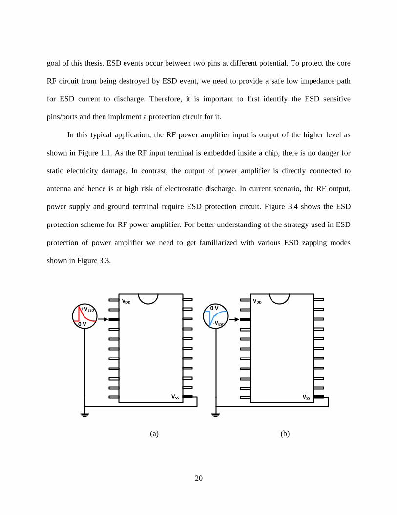
In this typical application, the RF power amplifier input is output of the higher level as
shown in Figure 1.1. As the RF input terminal is embedded inside a chip, there is no danger for
static electricity damage. In contrast, the output of power amplifier is directly connected to
antenna and hence is at high risk of electrostatic discharge. In current scenario, the RF output,
power supply and ground terminal require ESD protection circuit. Figure 3.4 shows the ESD
protection scheme for RF power amplifier. For better understanding of the strategy used in ESD
protection of power amplifier we need to get familiarized with various ESD zapping modes
shown in Figure 3.3.
(a) (b)
+VESD
0 V
VDD
VSS
-VESD
0 VVDD
VSS
21
(c) (d)
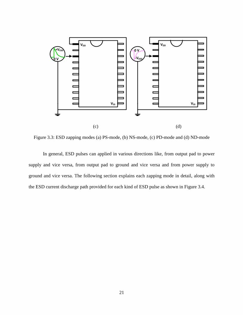
Figure 3.3: ESD zapping modes (a) PS-mode, (b) NS-mode, (c) PD-mode and (d) ND-mode
In general, ESD pulses can applied in various directions like, from output pad to power
supply and vice versa, from output pad to ground and vice versa and from power supply to
ground and vice versa. The following section explains each zapping mode in detail, along with
the ESD current discharge path provided for each kind of ESD pulse as shown in Figure 3.4.
+VESD
0 V
VDD
VSS
-VESD
0 V
VDD
VSS
22
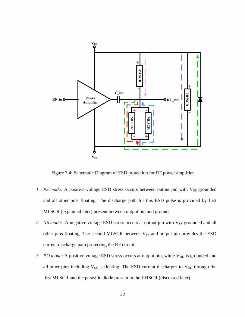
Figure 3.4: Schematic Diagram of ESD protection for RF power amplifier
1. PS mode: A positive voltage ESD stress occurs between output pin with VSS grounded
and all other pins floating. The discharge path for this ESD pulse is provided by first
MLSCR (explained later) present between output pin and ground.
2. NS mode: A negative voltage ESD stress occurs at output pin with VSS grounded and all
other pins floating. The second MLSCR between VSS and output pin provides the ESD
current discharge path protecting the RF circuit.
3. PD mode: A positive voltage ESD stress occurs at output pin, while VDD is grounded and
all other pins including VSS is floating. The ESD current discharges to VDD through the
first MLSCR and the parasitic diode present in the HHSCR (discussed later).
HH
SC
R
RF_outPower
AmplifierRF_in
VSS
VDD
ML
SC
R
ML
SC
R
ML
SC
RC_iso
+
+
- +
-
+
-
-
23
4. ND mode: A negative ESD stress occurs between output pin and grounded VDD while rest
of the pins including VSS is floating. Here, the transient ESD current is discharged by
third MLSCR present between VDD and output pin.
5. DS mode: The discharge path between VDD and VSS is provided by HHSCR, thereby
achieving the complete ESD protection of RF circuit.
The isolation capacitance seen in Figure 3.14 between PA and protection circuit acts as a
decoupling capacitor. A higher ESD voltage may be induced by current conduction via SCR and
this overshooting voltage may be greater than drain breakdown voltage. Therefore, isolation
capacitance is needed to block any direct connection between RF PA and ESD protection circuit.
I/O Pad ESD Protection
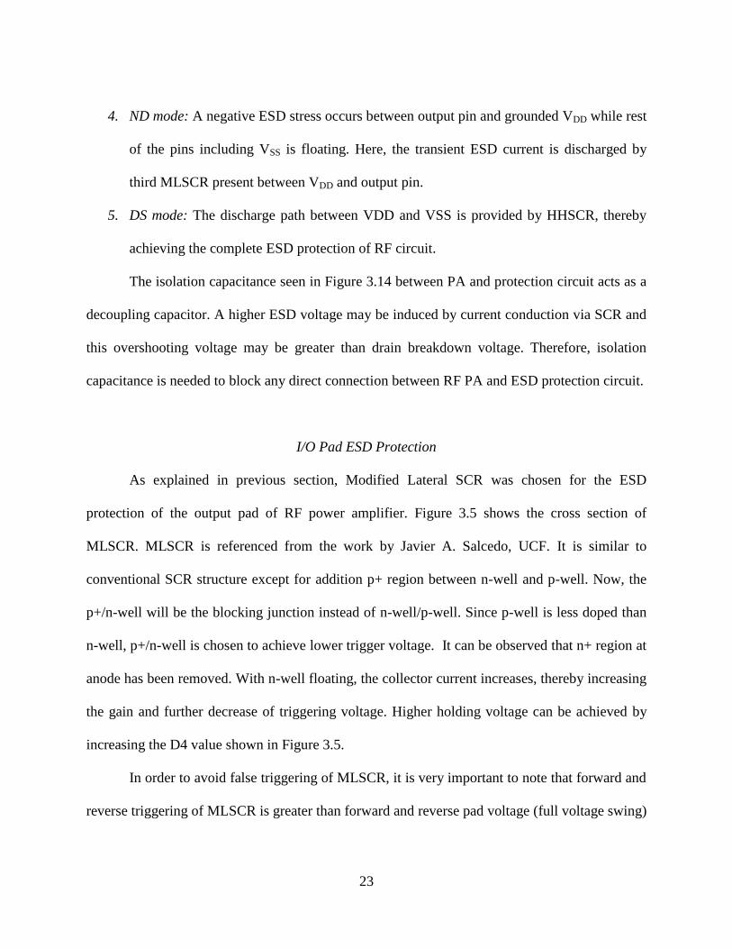
As explained in previous section, Modified Lateral SCR was chosen for the ESD
protection of the output pad of RF power amplifier. Figure 3.5 shows the cross section of
MLSCR. MLSCR is referenced from the work by Javier A. Salcedo, UCF. It is similar to
conventional SCR structure except for addition p+ region between n-well and p-well. Now, the
p+/n-well will be the blocking junction instead of n-well/p-well. Since p-well is less doped than
n-well, p+/n-well is chosen to achieve lower trigger voltage. It can be observed that n+ region at
anode has been removed. With n-well floating, the collector current increases, thereby increasing
the gain and further decrease of triggering voltage. Higher holding voltage can be achieved by
increasing the D4 value shown in Figure 3.5.
In order to avoid false triggering of MLSCR, it is very important to note that forward and
reverse triggering of MLSCR is greater than forward and reverse pad voltage (full voltage swing)
24
but should be less than secondary breakdown voltage. However, the holding voltage can be less
than output pad voltage as the current at the pad is lower and cannot sustain latch-up.
Figure 3.5: Cross-sectional view of MLSCR
The device size required to carry ESD current is dependent on test model. For HBM ESD
level of 2 kV, . With RHBM= 1.5kΩ, RON<<RHBM and therefore It2=
1.33A. Knowing that the current carrying capability of SCR is approximately, 70mA/µm, we can
easily calculate the required device size. Here, each MLSCR has 4 fingers, 50µm each and thus
can carry worst case ESD current of 14A providing protection for HBM level of 21kV.
Power Supply Clamp
SCR chosen for power clamp needs to have higher holding voltage due to two reasons:
(1) Due to lower holding voltage, SCR can be triggered during normal operation and (2) Once
the SCR discharges ESD current it should turn off, but this may not happen if holding voltage is
lower than supply voltage. Therefore, to avoid latch up problem, holding voltage
25
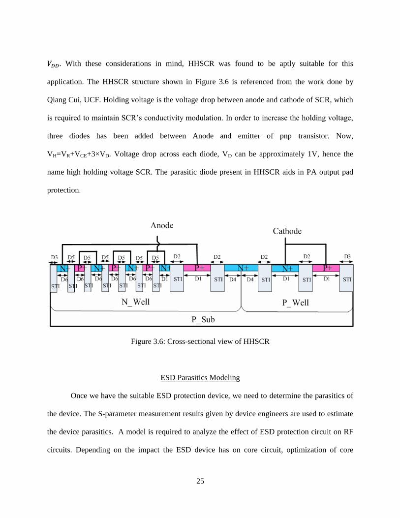
With these considerations in mind, HHSCR was found to be aptly suitable for this
application. The HHSCR structure shown in Figure 3.6 is referenced from the work done by
Qiang Cui, UCF. Holding voltage is the voltage drop between anode and cathode of SCR, which
is required to maintain SCR’s conductivity modulation. In order to increase the holding voltage,
three diodes has been added between Anode and emitter of pnp transistor. Now,
VH=VR+VCE+3×VD. Voltage drop across each diode, VD can be approximately 1V, hence the
name high holding voltage SCR. The parasitic diode present in HHSCR aids in PA output pad
protection.
Figure 3.6: Cross-sectional view of HHSCR
ESD Parasitics Modeling
Once we have the suitable ESD protection device, we need to determine the parasitics of
the device. The S-parameter measurement results given by device engineers are used to estimate
the device parasitics. A model is required to analyze the effect of ESD protection circuit on RF
circuits. Depending on the impact the ESD device has on core circuit, optimization of core
26
circuit can be done to improve the results. Further, using this model the transient analysis can be
performed to verify the HBM ESD robustness.
Figure 3.7: RC modeling of SCR device parasitics
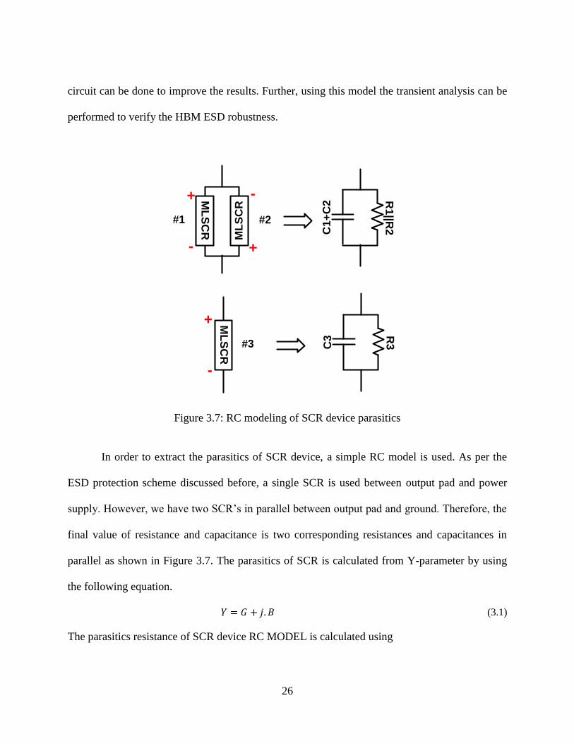
In order to extract the parasitics of SCR device, a simple RC model is used. As per the
ESD protection scheme discussed before, a single SCR is used between output pad and power
supply. However, we have two SCR’s in parallel between output pad and ground. Therefore, the
final value of resistance and capacitance is two corresponding resistances and capacitances in
parallel as shown in Figure 3.7. The parasitics of SCR is calculated from Y-parameter by using
the following equation.
(3.1)
The parasitics resistance of SCR device RC MODEL is calculated using
ML
SC
R
ML
SC
R
#1 #2
+
+-
-
C1+
C2
R1
||R2
ML
SC
R#3
+
-
C3
R3
27
(3.2)
The parasitic capacitance is extracted by using the following equation at frequency of 5.2GHz.
(3.3)
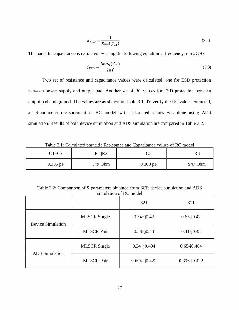
Two set of resistance and capacitance values were calculated, one for ESD protection
between power supply and output pad. Another set of RC values for ESD protection between
output pad and ground. The values are as shown in Table 3.1. To verify the RC values extracted,
an S-parameter measurement of RC model with calculated values was done using ADS
simulation. Results of both device simulation and ADS simulation are compared in Table 3.2.
Table 3.1: Calculated parasitic Resistance and Capacitance values of RC model
C1+C2 R1||R2 C3 R3
0.386 pF 549 Ohm 0.208 pF 947 Ohm
Table 3.2: Comparison of S-parameters obtained from SCR device simulation and ADS
simulation of RC model
S21 S11
Device Simulation
MLSCR Single 0.34+j0.42 0.65-j0.42
MLSCR Pair 0.58+j0.43 0.41-j0.43
ADS Simulation
MLSCR Single 0.34+j0.404 0.65-j0.404
MLSCR Pair 0.604+j0.422 0.396-j0.422
28
References
[1] S. Yu-Da, H. Bo-Shih, and K. Ming-Dou, "CMOS Power Amplifier with ESD Protection
Design Merged in Matching Network," in Electronics, Circuits and Systems, 2007. ICECS 2007.
14th IEEE International Conference on, 2007, pp. 825-828.
[2] S. Thijs, K. Raczkowski, D. Linten, M. Scholz, A. Griffoni, and G. Groeseneken, "CDM and
HBM analysis of ESD protected 60 GHz power amplifier in 45 nm low-power digital CMOS," in
EOS/ESD Symposium, 2009 31st, 2009, pp. 1-5.
[3] K. Ming-Dou, L. Chun-Yu, and M. Guo-Xuan, "ESD protection design for fully integrated
CMOS RF power amplifiers with waffle-structured SCR," in Circuits and Systems, 2008. ISCAS
2008. IEEE International Symposium on, 2008, pp. 1292-1295.
29
CHAPTER FOUR: ESD PROTECTED POWER AMPLIFIERS
Power Amplifier (PA) is an important candidate of the wireless transceiver. The RF
power amplifier is used to amplify the RF signal being transmitted to an adequate power level
such that it can propagate over a required distance through the wireless channel. In order to meet
the growing demands of low cost, low power and high capacity, CMOS process technology is
being widely used to implement RF-PA. In general, there is tradeoff between characteristics like
amplifier’s linearity and efficiency. Improving amplifier’s linearity will degrade its efficiency.
The standard industry defined metrics are used to characterize the performance of a PA.
Various metrics that are briefly explained in the following section help us evaluate how
efficiently the PA can amplify the signal with minimum distortion.
1. Output Power: The output power of an RF power amplifier is defined as the total power
of the RF signal delivered by the power amplifier to the load. For Sinusoidal signal, the
output power is given by
(4.1)
2. Efficiency: Power amplifier efficiency is a metric that indicates how efficiently power
drawn from the supply is converted to RF power delivered to the load [1]. Higher
efficiency means less power loss in the amplifier. Three most commonly equations used
to determine PA efficiency are:
(4.2)
30
(4.3)
(4.4)
Where, gives the total DC power drawn from the supply, Pin is the power
amplifier input power and PO is the output power of the amplifier.
3. Power Gain: The power Gain of an amplifier is the ratio of the output power to its input
power and is given by,
(4.5)
4. Linearity: Linear amplification is required when the signal contains both amplitude and
phase modulation. Linearity ensures that the original information is preserved and can be
later detected without any error. Depending on the application, Linearity can be
quantified using several different techniques such as Intermodulation distortion,1-dB
compression point or third-order Intercept point (IP3).
In general, there is a tradeoff between these characteristics like improving amplifier’s
linearity will degrade its efficiency.
Power Amplifier Classification/classes: Power amplifiers can be broadly classified into
current-mode Amplifiers and switching-mode Amplifiers, based on how the active device
behaves. Current-mode amplifiers, also called as transconductance PA, make use of the active
device as a transconductor. In this category, the active device acts as a voltage-controlled current
source, meaning its output current is controlled by its input voltage. While switching PA, uses
the active device as a switch to modulate the output voltage or current. Current-mode PAs
31
include classes A, AB, B, and C depending on the conduction angle. On the other hand,
switching amplifiers are divided into classes D, E and F.
Modeling of Class-A Power Amplifier with ESD
Class-A power amplifier is a linear amplifier, where the amplified output voltage is exact
replica of input voltage. Figure 4.1(a) shows a basic class-A power amplifier [2]. It consists of a
transistor as an amplifying device, RF choke, coupling capacitor and a parallel resonant circuit.
The transistor is used as a dependent current source and conducts all the time with conduction
angle 360°. At operating frequency, parallel resonant circuit at the load, filters out the harmonics
and reduces distortion due to large signal operation [2].
Figure 4.1: (a) Class-A power amplifier circuit, (b) Class-A PA with ESD protection circuit
In class-A power amplifier, the transistor is operating in active region, with gate to source
voltage greater than threshold voltage of the transistor. The Class-A power amplifier with ESD
shown in Figure 4.1(b) can be modeled with the following equations.
LD
vDS
Vgs
VGS
VDD
L C
Cc
R
IDD
io
iD
LD
vDS
Vgs
VGS
VDD
Cc
IDD
iD
L C R
io
CESD
RESD
Reff
iCesd
32
The drain current of Class-A power amplifier is given by,
(4.6)
where is the bias current and is the peak sinusoidal current.
is given by the drain current of an n-channel MOSFET
(4.7)
where is the electron mobility in the channel.
is the oxide capacitance and is given by
is the channel Width and is the channel width.
is the gate to source voltage
is the threshold voltage.
The drain voltage at the resonant frequency of the parallel resonant circuit is
(4.8)
where is the dc supply voltage and . Note that is the effective load
resistance, given by and in parallel.
An ideal parallel- resonant circuit L-C presents an infinite reactance at the resonant
frequency . By applying KCL, the ouput current at the resonant frequency is
(4.9)
(4.10)
The current through the ESD capacitor is
(4.11)
Finally, the output voltage at the resonant frequency is
(4.12)
33
Given these equations, Class-A power amplifier with ESD can be modeled for given
specifications. The class-A PA operating at 5.2GHz with load resistance of 50 ohm, supply
voltage of 3.3V and gate voltage of 1.2V was simulated using MATLAB. The ESD resistance
and capacitance were assumed to be 549 ohms and 0.386pf respectively.
For the same specification, a class-A power amplifier circuit was designed in ADS and
simulated. The drain current, drain voltage, output current and output voltage waveforms
obtained from both MATLAB and ADS simulation was almost identical. Both the simulation
results are shown below.
(a) (b)
Figure 4.2: Transient waveforms of Drain voltage (a) MATLAB, (b) ADS
Figure 4.3: Transient waveforms of Drain current (a) MATLAB, (b) ADS
99.080 99.099 99.119 99.138 99.158 99.177 99.197 99.216 99.23699.060 99.255
20
40
60
80
100
120
140
160
0
180
time, nsec
TR
AN
.ID
SM
1.i,
mA
(a) (b)
34
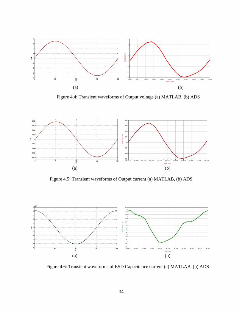
Figure 4.4: Transient waveforms of Output voltage (a) MATLAB, (b) ADS
(a) (b)
Figure 4.5: Transient waveforms of Output current (a) MATLAB, (b) ADS
(a) (b)
Figure 4.6: Transient waveforms of ESD Capacitance current (a) MATLAB, (b) ADS
99.070 99.089 99.109 99.128 99.148 99.167 99.187 99.206 99.22699.050 99.245
-2
-1
0
1
2
3
-3
4
time, nsec
TR
AN
.Vo
ut,
V
(a) (b)
99.070 99.089 99.109 99.128 99.148 99.167 99.187 99.206 99.22699.050 99.245
-40
-20
-0
20
40
60
-60
80
time, nsec
TR
AN
.Iou
t.i,
mA
99.070 99.089 99.109 99.128 99.148 99.167 99.187 99.206 99.22699.050 99.245
-50
-40
-30
-20
-10
0
10
20
30
40
-60
50
time, nsec
TR
AN
.Ies
dC.i,
uA
35
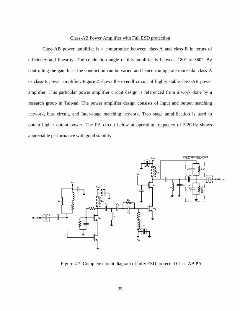
Class-AB Power Amplifier with Full ESD protection
Class-AB power amplifier is a compromise between class-A and class-B in terms of
efficiency and linearity. The conduction angle of this amplifier is between 180° to 360°. By
controlling the gate bias, the conduction can be varied and hence can operate more like class-A
or class-B power amplifier. Figure 2 shows the overall circuit of highly stable class-AB power
amplifier. This particular power amplifier circuit design is referenced from a work done by a
research group in Taiwan. The power amplifier design consists of Input and output matching
network, bias circuit, and Inter-stage matching network. Two stage amplification is used to
obtain higher output power. The PA circuit below at operating frequency of 5.2GHz shows
appreciable performance with good stability.
LD1
VG1
M1
M2
LG1R2
C2
Li
Ci2Ci1
LG2
VDD
VG2
VDD
LD2
M3
VDD
RF_in
LO
Cin
C0
RF_out
C_iso
R3
R1
||R2
C3
C1
+C
2
ESD Protection Circuit
Figure 4.7: Complete circuit diagram of fully ESD protected Class-AB PA.
36
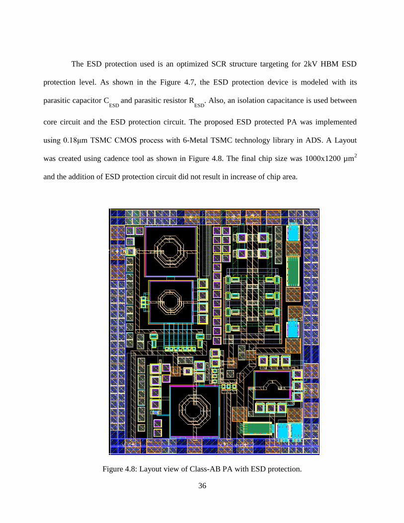
The ESD protection used is an optimized SCR structure targeting for 2kV HBM ESD
protection level. As shown in the Figure 4.7, the ESD protection device is modeled with its
parasitic capacitor CESD
and parasitic resistor RESD
. Also, an isolation capacitance is used between
core circuit and the ESD protection circuit. The proposed ESD protected PA was implemented
using 0.18μm TSMC CMOS process with 6-Metal TSMC technology library in ADS. A Layout
was created using cadence tool as shown in Figure 4.8. The final chip size was 1000x1200 µm2
and the addition of ESD protection circuit did not result in increase of chip area.
Figure 4.8: Layout view of Class-AB PA with ESD protection.
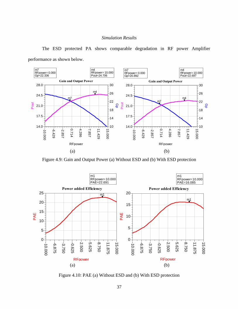
37
Simulation Results
The ESD protected PA shows comparable degradation in RF power Amplifier
performance as shown below.
Figure 4.9: Gain and Output Power (a) Without ESD and (b) With ESD protection
Figure 4.10: PAE (a) Without ESD and (b) With ESD protection
-6.4
29
-2.8
57
0.7
14
4.2
86
7.8
57
11
.42
9
-10
.00
0
15
.00
0
17.5
21.0
24.5
14.0
28.0
14
18
22
26
10
30
RFpower
Gp
0.00022.336
m7
Po
ut
10.00024.706
m4
Gain and Output Power
m7RFpower=Gp=22.336
0.000m4RFpower=Pout=24.706
10.000
-6.4
29
-2.8
57
0.7
14
4.2
86
7.8
57
11
.42
9
-10
.00
0
15
.00
0
17.5
21.0
24.5
14.0
28.0
14
18
22
26
10
30
RFpower
Gp
0.00020.892
m7
Po
ut
Readout
m4
Gain and Output Power
m7RFpower=Gp=20.892
0.000m4RFpower=Pout=22.697
10.000
-6.8
75
-3.7
50
-0.6
25
2.5
00
5.6
25
8.7
50
11
.87
5
-10
.00
0
15
.00
0
5
10
15
20
0
25
RFpower
PA
E
Readout
m1
Power added Efficiency
m1RFpower=PAE=22.691
10.000
-6.8
75
-3.7
50
-0.6
25
2.5
00
5.6
25
8.7
50
11
.87
5
-10
.00
0
15
.00
0
5
10
15
0
20
RFpower
PA
E
Readout
m1
Power added Efficiency
m1RFpower=PAE=16.085
10.000
(a) (b)
(a) (b)
38
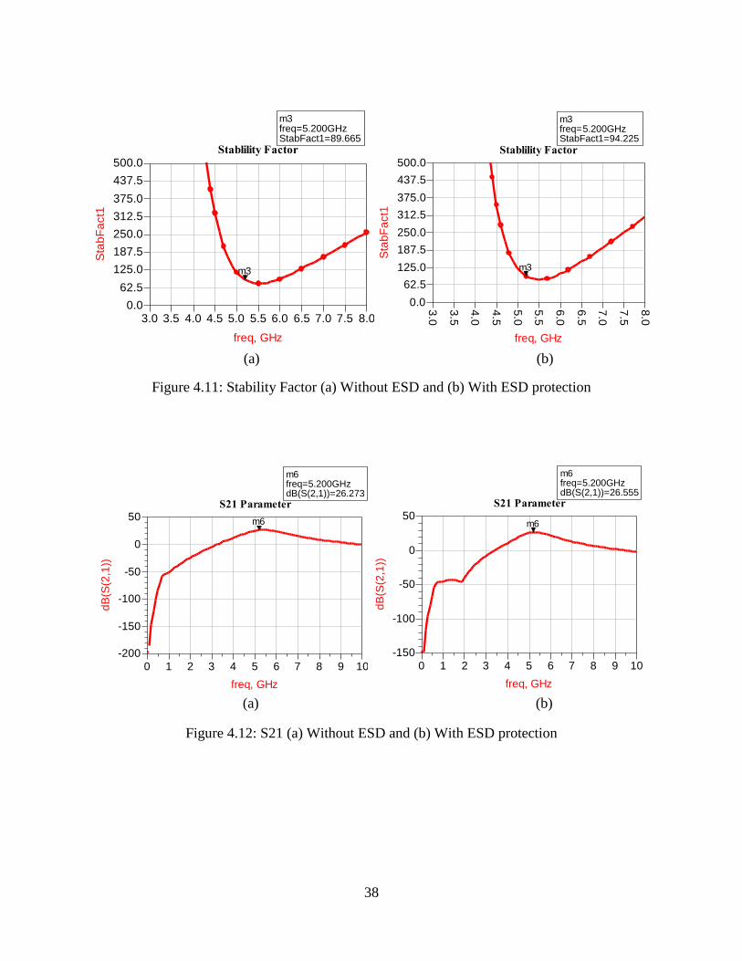
Figure 4.11: Stability Factor (a) Without ESD and (b) With ESD protection
Figure 4.12: S21 (a) Without ESD and (b) With ESD protection
3.5 4.0 4.5 5.0 5.5 6.0 6.5 7.0 7.53.0 8.0
62.5
125.0
187.5
250.0
312.5
375.0
437.5
0.0
500.0
freq, GHz
Sta
bF
act1
Readout
m3
Stablility Factor
m3freq=StabFact1=89.665
5.200GHz
3.5
4.0
4.5
5.0
5.5
6.0
6.5
7.0
7.5
3.0
8.0
62.5
125.0
187.5
250.0
312.5
375.0
437.5
0.0
500.0
freq, GHz
Sta
bF
act1
Readout
m3
Stablility Factor
m3freq=StabFact1=94.225
5.200GHz
1 2 3 4 5 6 7 8 90 10
-150
-100
-50
0
-200
50
freq, GHz
dB
(S(2
,1))
5.200G26.27
m6
S21 Parameter
m6freq=dB(S(2,1))=26.273
5.200GHz
1 2 3 4 5 6 7 8 90 10
-100
-50
0
-150
50
freq, GHz
dB
(S(2
,1))
Readout
m6
S21 Parameter
m6freq=dB(S(2,1))=26.555
5.200GHz
(a) (b)
(a) (b)
39
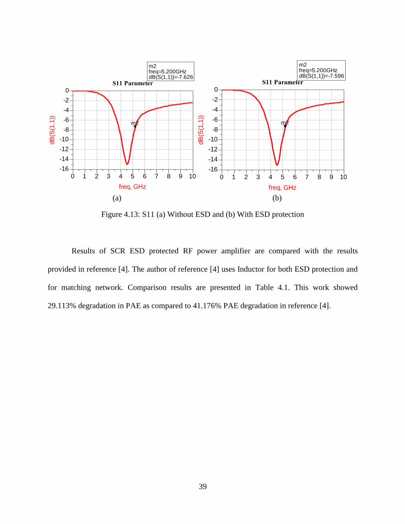
Figure 4.13: S11 (a) Without ESD and (b) With ESD protection
Results of SCR ESD protected RF power amplifier are compared with the results
provided in reference [4]. The author of reference [4] uses Inductor for both ESD protection and
for matching network. Comparison results are presented in Table 4.1. This work showed
29.113% degradation in PAE as compared to 41.176% PAE degradation in reference [4].
1 2 3 4 5 6 7 8 90 10
-14
-12
-10
-8
-6
-4
-2
-16
0
freq, GHz
dB
(S(1
,1))
Readout
m2
S11 Parameter
m2freq=dB(S(1,1))=-7.626
5.200GHz
1 2 3 4 5 6 7 8 90 10
-14
-12
-10
-8
-6
-4
-2
-16
0
freq, GHz
dB
(S(1
,1))
Readout
m2
S11 Parameter
m2freq=dB(S(1,1))=-7.596
5.200GHz
(a) (b)
40
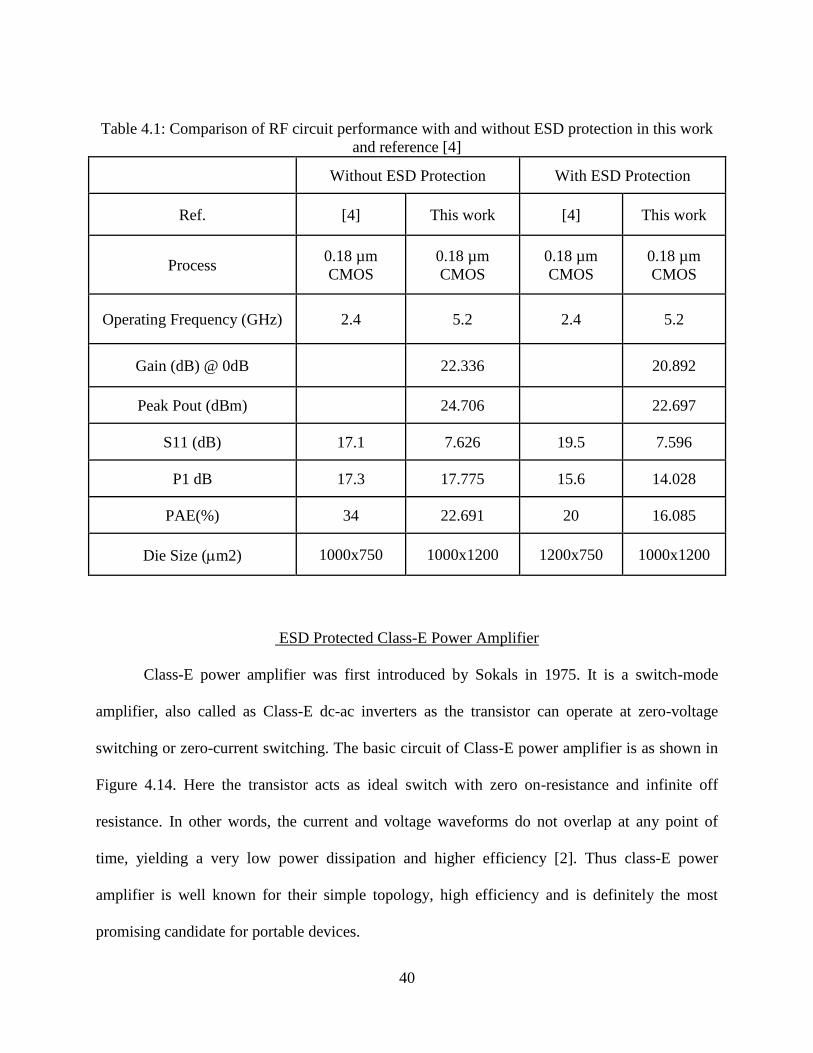
Table 4.1: Comparison of RF circuit performance with and without ESD protection in this work
and reference [4]
Without ESD Protection With ESD Protection
Ref. [4] This work [4] This work
Process 0.18 µm
CMOS
0.18 µm
CMOS
0.18 µm
CMOS
0.18 µm
CMOS
Operating Frequency (GHz) 2.4 5.2 2.4 5.2
Gain (dB) @ 0dB
22.336
20.892
Peak Pout (dBm)
24.706
22.697
S11 (dB) 17.1 7.626 19.5 7.596
P1 dB 17.3 17.775 15.6 14.028
PAE(%) 34 22.691 20 16.085
Die Size (m2) 1000x750 1000x1200 1200x750 1000x1200
ESD Protected Class-E Power Amplifier
Class-E power amplifier was first introduced by Sokals in 1975. It is a switch-mode
amplifier, also called as Class-E dc-ac inverters as the transistor can operate at zero-voltage
switching or zero-current switching. The basic circuit of Class-E power amplifier is as shown in
Figure 4.14. Here the transistor acts as ideal switch with zero on-resistance and infinite off
resistance. In other words, the current and voltage waveforms do not overlap at any point of
time, yielding a very low power dissipation and higher efficiency [2]. Thus class-E power
amplifier is well known for their simple topology, high efficiency and is definitely the most
promising candidate for portable devices.
41
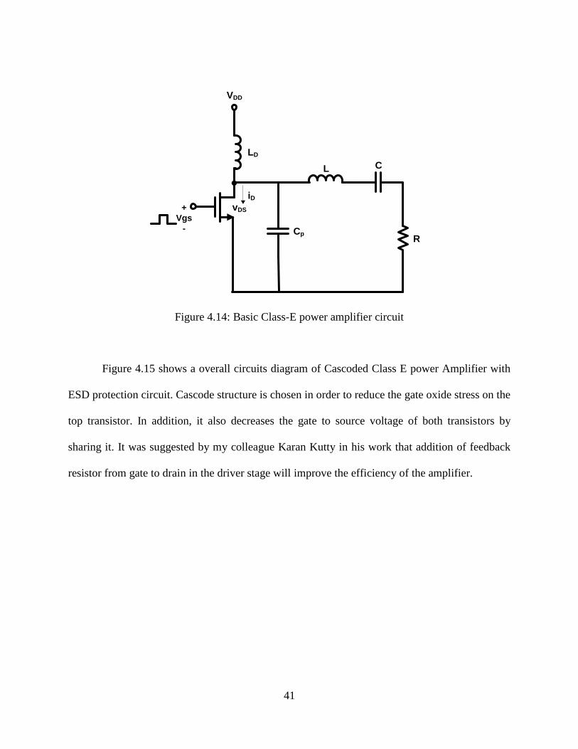
Figure 4.14: Basic Class-E power amplifier circuit
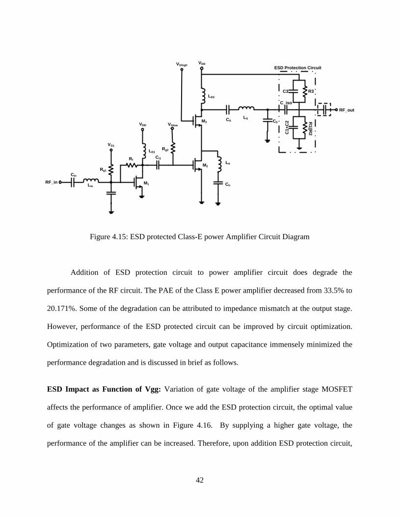
Figure 4.15 shows a overall circuits diagram of Cascoded Class E power Amplifier with
ESD protection circuit. Cascode structure is chosen in order to reduce the gate oxide stress on the
top transistor. In addition, it also decreases the gate to source voltage of both transistors by
sharing it. It was suggested by my colleague Karan Kutty in his work that addition of feedback
resistor from gate to drain in the driver stage will improve the efficiency of the amplifier.
LD
vDS
VDD
R
iD
CL
Cp
+
Vgs
-
42
Figure 4.15: ESD protected Class-E power Amplifier Circuit Diagram
Addition of ESD protection circuit to power amplifier circuit does degrade the
performance of the RF circuit. The PAE of the Class E power amplifier decreased from 33.5% to
20.171%. Some of the degradation can be attributed to impedance mismatch at the output stage.
However, performance of the ESD protected circuit can be improved by circuit optimization.
Optimization of two parameters, gate voltage and output capacitance immensely minimized the
performance degradation and is discussed in brief as follows.
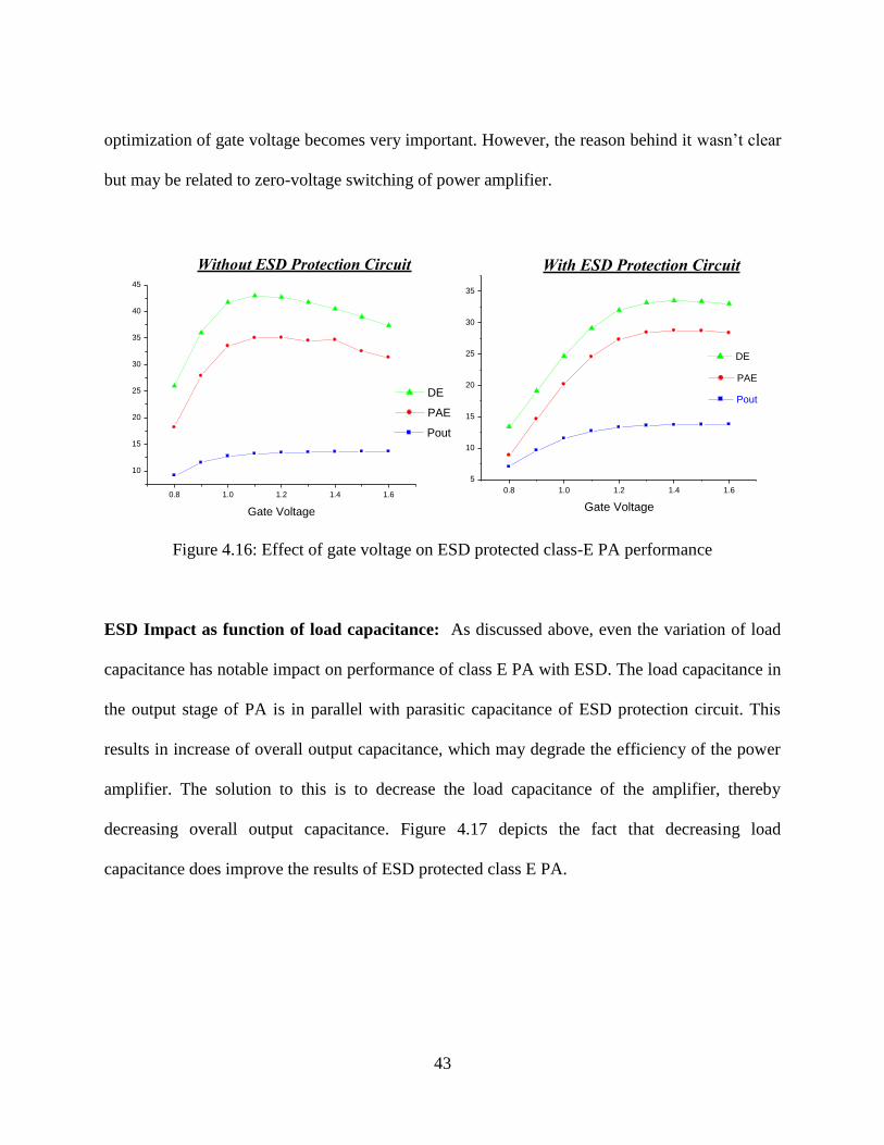
ESD Impact as Function of Vgg: Variation of gate voltage of the amplifier stage MOSFET
affects the performance of amplifier. Once we add the ESD protection circuit, the optimal value
of gate voltage changes as shown in Figure 4.16. By supplying a higher gate voltage, the
performance of the amplifier can be increased. Therefore, upon addition ESD protection circuit,
C0
RF_out
C_iso
R3R
1||R
2C3
C1+
C2
ESD Protection Circuit
M2Ltr
LS
RF_in
Cin
Lin
VG1
LD1
M1
Ci1
VDD VGlow
LD2
VGhigh
M3
VDD
Ctr
CS
Rf
Rg1
Rg2
43
optimization of gate voltage becomes very important. However, the reason behind it wasn’t clear
but may be related to zero-voltage switching of power amplifier.
Figure 4.16: Effect of gate voltage on ESD protected class-E PA performance
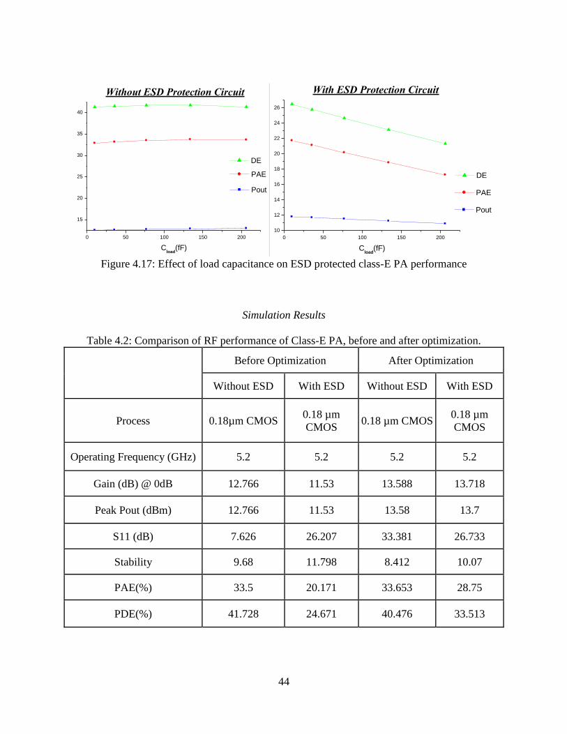
ESD Impact as function of load capacitance: As discussed above, even the variation of load
capacitance has notable impact on performance of class E PA with ESD. The load capacitance in
the output stage of PA is in parallel with parasitic capacitance of ESD protection circuit. This
results in increase of overall output capacitance, which may degrade the efficiency of the power
amplifier. The solution to this is to decrease the load capacitance of the amplifier, thereby
decreasing overall output capacitance. Figure 4.17 depicts the fact that decreasing load
capacitance does improve the results of ESD protected class E PA.
0.8 1.0 1.2 1.4 1.6
10
15
20
25
30
35
40
45
Without ESD Protection Circuit
DE
PAE
Gate Voltage
Pout
0.8 1.0 1.2 1.4 1.6
5
10
15
20
25
30
35
With ESD Protection Circuit
DE
PAE
Gate Voltage
Pout
44
Figure 4.17: Effect of load capacitance on ESD protected class-E PA performance
Simulation Results
Table 4.2: Comparison of RF performance of Class-E PA, before and after optimization.
Before Optimization After Optimization
Without ESD With ESD Without ESD With ESD
Process 0.18µm CMOS 0.18 µm
CMOS 0.18 µm CMOS
0.18 µm
CMOS
Operating Frequency (GHz) 5.2 5.2 5.2 5.2
Gain (dB) @ 0dB 12.766 11.53 13.588 13.718
Peak Pout (dBm) 12.766 11.53 13.58 13.7
S11 (dB) 7.626 26.207 33.381 26.733
Stability 9.68 11.798 8.412 10.07
PAE(%) 33.5 20.171 33.653 28.75
PDE(%) 41.728 24.671 40.476 33.513
0 50 100 150 200
15
20
25
30
35
40
Pout
PAE
Without ESD Protection Circuit
Cload
(fF)
DE
0 50 100 150 200
10
12
14
16
18
20
22
24
26
With ESD Protection Circuit
DE
PAE
Cload
(fF)
Pout
45
References
[1] Shirvani, Alireza and Wooley, Bruce A. Design and Control of RF Power Amplifiers.
Kluwer Academic Publishers, 2003.
[2] Kazimierczuk, Marian K. RF Power Amplifiers. West Sussex: John Wiley & Sons, 2008.
[3] Grebennikov, Andrei. RF and Microwave Power Amplifier Design. McGraw-Hill, 2005
[4] S. Yu-Da, H. Bo-Shih, and K. Ming-Dou, "CMOS Power Amplifier with ESD Protection
Design Merged in Matching Network," in Electronics, Circuits and Systems, 14th IEEE
International Conference on, 2007, pp. 825-828
46
CHAPTER FIVE: CONCLUSION
The preliminary research began with in-depth understanding of various existing ESD
protection methods. Later, we implemented already existing ESD protected LNA to study the
ESD impact on LNA circuit performance. In the process, the studies revealed that not much
research has been done towards ESD protection of RF power amplifiers as compared to LNA.
The ESD robustness and the RF circuit performance degradation of all available ESD protection
technique was evaluated using RF power amplifier circuit and the results were compared.
As high speed CMOS technologies require ESD protection with high protection level and
low parasitics, SCR was found to be ideal choice. SCR offers highest ESD protection level per
unit area with low parasitics and smaller area. The modified SCR’s with low triggering voltage
for I/O protection and with high holding voltage for supply clamp was chosen for ESD
protection of RF power amplifiers. Analytical equations were derived from the ESD protected
linear power amplifier model. The numerically solved MATLAB results agreed with the ADS
simulated results. Further, a complete ESD protection was implemented to Class-AB power
amplifier and circuit simulations were performed using the calculated RC model of SCR.
Comparison of PA performance with and without ESD helped in evaluation of ESD effect on RF
power amplifiers.
Additionally, the SCR based ESD protection circuit was added to switch-mode Class-E
power amplifier. Even though there was considerable degradation in class-E PA performance,
the circuit optimization improved the power amplifier results significantly.
47
CHAPTER SIX: FUTURE WORK
The most significant part of ESD design is testing the ESD protected circuit. The fully
protected class-AB power amplifier has to be commercially fabricated and tested with 2kV HBM
pulse. The chip can also be used to measure the complete RF circuit performance. The analytical
equations derived for ESD protected linear power amplifier model can be used to as base to
derive the same for Class-E power amplifier. This model will aid in further optimization of the
PA circuit to decrease the ESD circuit impact on amplifier’s performance. Lastly, the ESD
protected power amplifier can also be tested for Machine Model ESD robustness.