Embed Size (px)
Citation preview
FACULDADE DE ENGENHARIA DA UNIVERSIDADE DO PORTO
Study and implementation of optimizedsolutions for re-configurable logic over
ASIC design flow
Ricardo Azevedo Araújo
FOR JURY EVALUATION
Mestrado Integrado em Engenharia Electrotécnica e de Computadores
Supervisor: Prof. João Canas Ferreira
Second Advisor: Eng. Luis Cruz
July 28, 2018

c© Ricardo Azevedo Araújo, 2018
Resumo
Os ASICs são circuitos integrados projetados para um uso específico e geralmente implementadosusando um fluxo de projeto baseado em standard-cell. Esse fluxo de design geralmente requervalidação extensiva antes da fabricação, mas com a procura atual por ciclos de desenvolvimentomais rápidos, uma grande parte dos testes de interoperabilidade de testes é executada em silícioreal. Devido à lógica fixa do circuito final, é impossível realizar pequenas atualizações do projeto.
O desenvolvimento de um chip usando esse método requer muito tempo e impõe custos sub-stanciais, já que um conjunto único de máscaras é necessário para ser produzido cada vez queum protótipo é fabricado. Apesar dos testes intensos, os problemas podem ser descobertos apóso tapeout devido a depuração de laboratório ou verificação contínua. Como resultado, um novoprojeto é realizado para resolver o problema e um novo protótipo é necessário para testar o novochip. Como um novo conjunto de máscaras é necessário, o custo de produção aumenta. Se o chippuder ser produzido usando lógica programável e erros inesperados aparecerem durante o teste,os designers podem corrigi-lo, o que impede o descarte de chips. Um dos exemplos é a nova ondade FPGAs rápidos que permitiram testar alguns dos códigos ASIC antes de iniciar a produção demáscaras, embora exista sempre uma pequena parte do design que, devido à natureza específicadas freqüências operacionais, requer implementação em tempo real na Silício para a prototipagem.
O objetivo deste trabalho de dissertação, como proposto pela Synopsys, é pesquisar maneiraspelas quais módulos específicos de um projeto ASIC são substituídos por uma lógica reconfig-urável implementada com um subconjunto limitado de standard-cell. O uso será direcionado paraa lógica de controlo, que normalmente possui requisitos de frequência mais baixos do que o dat-apath. O trabalho concentrou-se num fluxo que minimiza o envolvimento do designer de ASICRTL e atende aos requisitos de verificação.
O resultado desta tese é um fluxo de projeto que é capaz de traduzir uma representação es-tática de uma determinada RTL em uma reconfigurável que suporta mudanças pós-fabricação paradebugging. Para criar o circuito reconfigurável, é utilizada uma arquitectura baseada em termosde produto (PTB). Essa arquitetura tem um conjunto de planos de porta AND programáveis quese conectam a um conjunto de planos de porta OR programáveis e a saída do circuito é a saída dasportas OR. Tem a característica de ser mais simples e, portanto, menor em termos de área para pro-jetos mais compactos do que uma arquitetura baseada em LUT, já que requer menos mecanismode roteamento. No entanto, é mais limitado em termos de funcionalidade.
Para converter o ASIC em um dispositivo programável capaz de debugging pós-fabricaçãousando esta arquitetura, três soluções foram estudadas e testadas: uma solução totalmente re-configurável capaz de qualquer alteração (sem entradas adicionais, saídas ou aumentando muitoa complexidade do projeto), um solução parcialmente reconfigurável onde alguns módulos sãodeixados com lógica fixa e uma solução alternativa onde pequenos módulos programáveis são cri-ados separadamente capazes de substituir qualquer saída única. Dos três, o único que deu bonsresultados em termos de áreas foi a terceira solução.
i

ii
Abstract
ASICs are integrated circuits designed for a specific use and usually implemented using a standard-cell based design flow. This design flow often requires extensive validation prior to fabrication,but with the current demand for faster turn-around development cycles a big portion of the testsinteroperability tests is performed in actual silicon. Due to the fixed logic functionality of the finalcircuit it is impossible to perform small updates of the design.
The development of a chip using this method requires a lot of time and imposes substantialcosts, as a unique mask set is needed to be produced each time a prototype is fabricated. De-spite the intense testing, problems can be discovered after tapeout due to lab debug or continuousverification. As a result a new design is undertaken to resolve the problem and a new prototypeis needed to test the new chip. As a new mask set is needed, the production cost rises. If thechip could be produced using programmable logic and unexpected errors appears during testing,developers can debug and correct them on the field which prevents chip disposal. One of the ex-amples is the new wave of fast FPGAs that have allowed testing some of the ASIC code beforegoing into mask production, although there is always a small portion of the design that due to thespecific nature of the operating frequencies requires implementation in actual Silicon to enableprototyping.
The objective of this dissertion work, as proposed by Synopsys, is to research ways by whichspecific modules of an ASIC design are replaced by reconfigurable logic implemented with alimited sub-set of standard cells. The usage will be targeted to control logic, which has typicallylower frequency requirements than datapath. The work focused on a flow that minimizes theinvolvement of the ASIC RTL designer and complies with the verification requirements.
The result of this dissertion is a design flow which is capable of translating a static representa-tion of a given RTL into a reconfigurable one that supports post-fabrication changes for debuging.To create the reconfigurable circuit, a Product Term Based (PTB) architecture is used. This ar-chitecture has a set of programmable AND gate planes that link to a set of programmable ORgate planes and the output of the circuit is the output of the OR gates. It has the characteristic ofbeing simpler and therefore smaller for more compact designs than a LUT-based architeture as itrequires less routing mechanism. However it is more limited in terms of functinality.
To convert the ASIC into a programmable device capable of post-fabrication debuging usingthis architecture, three solutions were studied and tested: a fully reconfigurable solution capable ofany change (without aditional inputs, outputs or greatly increasing the complexity of the design),a partially reconfigurable solution where some modules are left with fixed logic and an alternativesolution where small programmable modules are created separately capable of overriding anysingle output. Of the three the only one that gave good results in terms of areas was the thirdsolution.
iii

iv
Contents
1 Introduction 11.1 Context . . . . . . . . . . . . . . . . . . . . . . . . . . . . . . . . . . . . . . . 11.2 Motivation . . . . . . . . . . . . . . . . . . . . . . . . . . . . . . . . . . . . . . 11.3 Objective of the thesis . . . . . . . . . . . . . . . . . . . . . . . . . . . . . . . . 21.4 Approach to the problem . . . . . . . . . . . . . . . . . . . . . . . . . . . . . . 21.5 Structure . . . . . . . . . . . . . . . . . . . . . . . . . . . . . . . . . . . . . . . 3
2 Background Knowledge and Literature Review 52.1 Introduction . . . . . . . . . . . . . . . . . . . . . . . . . . . . . . . . . . . . . 52.2 Application-Specific Integrated Circuits (ASIC) . . . . . . . . . . . . . . . . . . 6
2.2.1 ASIC design flow . . . . . . . . . . . . . . . . . . . . . . . . . . . . . . 62.3 Field Programmable Gate Array (FPGA) . . . . . . . . . . . . . . . . . . . . . 7
2.3.1 FPGA Architecture . . . . . . . . . . . . . . . . . . . . . . . . . . . . . 82.3.2 Look-up Table . . . . . . . . . . . . . . . . . . . . . . . . . . . . . . . 92.3.3 FPGA Design Flow . . . . . . . . . . . . . . . . . . . . . . . . . . . . . 9
2.4 Standard-Cell-based programmable logic core . . . . . . . . . . . . . . . . . . . 102.5 Programmable Logic Array . . . . . . . . . . . . . . . . . . . . . . . . . . . . . 12
2.5.1 ABC . . . . . . . . . . . . . . . . . . . . . . . . . . . . . . . . . . . . 132.5.2 Inputs and ABC commands . . . . . . . . . . . . . . . . . . . . . . . . 142.5.3 File output . . . . . . . . . . . . . . . . . . . . . . . . . . . . . . . . . 15
2.6 Conclusion . . . . . . . . . . . . . . . . . . . . . . . . . . . . . . . . . . . . . 16
3 Description of the Proposed Programmable Architecture 173.1 Introduction . . . . . . . . . . . . . . . . . . . . . . . . . . . . . . . . . . . . . 173.2 Architecture description . . . . . . . . . . . . . . . . . . . . . . . . . . . . . . . 18
3.2.1 Product Term Based Architecture . . . . . . . . . . . . . . . . . . . . . 193.2.2 Routing mechanisms and bitstream generation . . . . . . . . . . . . . . 20
3.3 Reconfigurable PTB improvements for specific circuits . . . . . . . . . . . . . . 223.3.1 Case 1: Only take sequential logic of the design into account . . . . . . . 233.3.2 Case 2: Only take combinational logic of the design into account . . . . . 233.3.3 Case 3: Module in the design has registers as outputs and its functionality
does not change . . . . . . . . . . . . . . . . . . . . . . . . . . . . . . . 233.3.4 Case 4: Module in the design has registers as outputs and but its inputs do
not change . . . . . . . . . . . . . . . . . . . . . . . . . . . . . . . . . 243.3.5 Case 5: Module in the design has extra inputs or outputs which could be
used in the future . . . . . . . . . . . . . . . . . . . . . . . . . . . . . . 243.3.6 Alternative: Create a separate module which overrides the outputs of the
ASIC . . . . . . . . . . . . . . . . . . . . . . . . . . . . . . . . . . . . 25
v
vi CONTENTS
3.4 Conclusions . . . . . . . . . . . . . . . . . . . . . . . . . . . . . . . . . . . . . 25
4 Design Flow Description 274.1 Introduction . . . . . . . . . . . . . . . . . . . . . . . . . . . . . . . . . . . . . 274.2 Verilog to PLA . . . . . . . . . . . . . . . . . . . . . . . . . . . . . . . . . . . 284.3 Circuit generation program . . . . . . . . . . . . . . . . . . . . . . . . . . . . . 29
4.3.1 Reconfigurable matrix creation . . . . . . . . . . . . . . . . . . . . . . . 294.3.2 Netlist generation . . . . . . . . . . . . . . . . . . . . . . . . . . . . . . 304.3.3 Bitstream generation . . . . . . . . . . . . . . . . . . . . . . . . . . . . 324.3.4 Verification of generated circuit . . . . . . . . . . . . . . . . . . . . . . 324.3.5 Inputs and Outputs . . . . . . . . . . . . . . . . . . . . . . . . . . . . . 33
4.4 Reconfiguration of the generated module . . . . . . . . . . . . . . . . . . . . . . 334.5 Conclusions . . . . . . . . . . . . . . . . . . . . . . . . . . . . . . . . . . . . . 34
5 Support tools used in the design flow 355.1 RTL parser . . . . . . . . . . . . . . . . . . . . . . . . . . . . . . . . . . . . . 355.2 Design Compiler . . . . . . . . . . . . . . . . . . . . . . . . . . . . . . . . . . 355.3 GTECH parser . . . . . . . . . . . . . . . . . . . . . . . . . . . . . . . . . . . 365.4 ODIN II . . . . . . . . . . . . . . . . . . . . . . . . . . . . . . . . . . . . . . . 365.5 Formality . . . . . . . . . . . . . . . . . . . . . . . . . . . . . . . . . . . . . . 37
5.5.1 TCL cript . . . . . . . . . . . . . . . . . . . . . . . . . . . . . . . . . . 375.5.2 Verification process . . . . . . . . . . . . . . . . . . . . . . . . . . . . . 38
6 Implementation and Results 396.1 Programmable Device Flow . . . . . . . . . . . . . . . . . . . . . . . . . . . . 39
6.1.1 ABC . . . . . . . . . . . . . . . . . . . . . . . . . . . . . . . . . . . . 406.1.2 Netlist generation . . . . . . . . . . . . . . . . . . . . . . . . . . . . . . 41
6.2 Device Reconfiguration . . . . . . . . . . . . . . . . . . . . . . . . . . . . . . . 426.3 Results and analysis . . . . . . . . . . . . . . . . . . . . . . . . . . . . . . . . . 43
6.3.1 Preliminary results . . . . . . . . . . . . . . . . . . . . . . . . . . . . . 436.3.2 Fully reconfigurable approach . . . . . . . . . . . . . . . . . . . . . . . 446.3.3 Partially reconfigurable approach . . . . . . . . . . . . . . . . . . . . . 456.3.4 Alternative approach . . . . . . . . . . . . . . . . . . . . . . . . . . . . 476.3.5 Conclusion . . . . . . . . . . . . . . . . . . . . . . . . . . . . . . . . . 50
7 Conclusions and Future work 53
A Design flow example 57A.1 Work directory . . . . . . . . . . . . . . . . . . . . . . . . . . . . . . . . . . . 57A.2 Running the design flow script . . . . . . . . . . . . . . . . . . . . . . . . . . . 58A.3 Programmable matrix generation . . . . . . . . . . . . . . . . . . . . . . . . . . 58
A.3.1 Fully reconfigurable . . . . . . . . . . . . . . . . . . . . . . . . . . . . 58A.3.2 Partially reconfigurable . . . . . . . . . . . . . . . . . . . . . . . . . . . 59A.3.3 Alternative . . . . . . . . . . . . . . . . . . . . . . . . . . . . . . . . . 59
A.4 Ful synthesis process . . . . . . . . . . . . . . . . . . . . . . . . . . . . . . . . 60
References 61
List of Figures
2.1 ASIC design flow . . . . . . . . . . . . . . . . . . . . . . . . . . . . . . . . . . 62.2 FPGA architecture . . . . . . . . . . . . . . . . . . . . . . . . . . . . . . . . . 82.3 Basic FPGA logic Element and logic cluster . . . . . . . . . . . . . . . . . . . . 92.4 Purpose Flow . . . . . . . . . . . . . . . . . . . . . . . . . . . . . . . . . . . . 102.5 Architeture overview . . . . . . . . . . . . . . . . . . . . . . . . . . . . . . . . 112.6 Programmable Logic Array . . . . . . . . . . . . . . . . . . . . . . . . . . . . . 122.7 AIG example . . . . . . . . . . . . . . . . . . . . . . . . . . . . . . . . . . . . 132.8 Pre-computed AIGs . . . . . . . . . . . . . . . . . . . . . . . . . . . . . . . . . 132.9 Simple AIG rewriting . . . . . . . . . . . . . . . . . . . . . . . . . . . . . . . . 142.10 Refactoring . . . . . . . . . . . . . . . . . . . . . . . . . . . . . . . . . . . . . 142.11 PLA example . . . . . . . . . . . . . . . . . . . . . . . . . . . . . . . . . . . . 15
3.1 Two possible aproach to create a better optimized reconfigurable circuit . . . . . 173.2 Programmable architecture (combinational logic only) . . . . . . . . . . . . . . 193.3 Programmable architecture . . . . . . . . . . . . . . . . . . . . . . . . . . . . . 203.4 Configuration plane and AND plane of a simple case . . . . . . . . . . . . . . . 213.6 Case 1 . . . . . . . . . . . . . . . . . . . . . . . . . . . . . . . . . . . . . . . . 233.7 Case 2 . . . . . . . . . . . . . . . . . . . . . . . . . . . . . . . . . . . . . . . . 233.8 Case 3 . . . . . . . . . . . . . . . . . . . . . . . . . . . . . . . . . . . . . . . . 243.9 Case 4 . . . . . . . . . . . . . . . . . . . . . . . . . . . . . . . . . . . . . . . . 243.10 Case 5 . . . . . . . . . . . . . . . . . . . . . . . . . . . . . . . . . . . . . . . . 253.11 Case 6 . . . . . . . . . . . . . . . . . . . . . . . . . . . . . . . . . . . . . . . . 25
4.1 Flows created . . . . . . . . . . . . . . . . . . . . . . . . . . . . . . . . . . . . 274.2 Verilog to PLA . . . . . . . . . . . . . . . . . . . . . . . . . . . . . . . . . . . 284.3 PLA format example . . . . . . . . . . . . . . . . . . . . . . . . . . . . . . . . 294.4 Static to fully reconfigurable conversion . . . . . . . . . . . . . . . . . . . . . . 304.5 Targeted reconfigurability . . . . . . . . . . . . . . . . . . . . . . . . . . . . . . 304.6 Netlist generation algorithm . . . . . . . . . . . . . . . . . . . . . . . . . . . . 314.7 Algoritms used for AND and OR plane . . . . . . . . . . . . . . . . . . . . . . 314.8 Bitstream algorithm . . . . . . . . . . . . . . . . . . . . . . . . . . . . . . . . . 324.9 verification . . . . . . . . . . . . . . . . . . . . . . . . . . . . . . . . . . . . . 334.10 Configuration of generated module flow . . . . . . . . . . . . . . . . . . . . . . 34
5.1 Design Compiler uses . . . . . . . . . . . . . . . . . . . . . . . . . . . . . . . . 36
6.1 Circuit to netlist conversion . . . . . . . . . . . . . . . . . . . . . . . . . . . . . 416.2 Cases for partial reconfiguration . . . . . . . . . . . . . . . . . . . . . . . . . . 466.3 Design is synthesized normally alongside a small reconfigurable module . . . . . 47
vii

viii LIST OF FIGURES
7.1 Routing between PTBs . . . . . . . . . . . . . . . . . . . . . . . . . . . . . . . 547.2 Output override has different optimized modules . . . . . . . . . . . . . . . . . 55
A.1 Work directory of the proposed design flow . . . . . . . . . . . . . . . . . . . . 57
List of Tables
4.1 Inputs and outputs of the Verilog to PLA phase . . . . . . . . . . . . . . . . . . 294.2 Reconfigurable connection to bitstream conversion . . . . . . . . . . . . . . . . 324.3 Inputs and outputs of the Netlist generation phase . . . . . . . . . . . . . . . . . 33
6.1 ABC aliases . . . . . . . . . . . . . . . . . . . . . . . . . . . . . . . . . . . . . 406.2 Impact on logic levels of the different aliases . . . . . . . . . . . . . . . . . . . 406.3 Circuit size in terms of logic levels, inputs, outputs and flip-flops . . . . . . . . . 436.4 Area comparison between original ASIC and the programmable circuit . . . . . . 446.5 Area and flip-flop increase broken down into different categories . . . . . . . . . 446.6 Data arrival time comparison for each test circuit . . . . . . . . . . . . . . . . . 456.7 Power comparisom between original ASIC and the programmable circuit . . . . 456.8 Power increase broken down into different categories . . . . . . . . . . . . . . . 456.9 Flip-flop count comparison . . . . . . . . . . . . . . . . . . . . . . . . . . . . . 466.10 Flip-flop count comparison . . . . . . . . . . . . . . . . . . . . . . . . . . . . . 466.11 Circuit size in terms of logic levels, inputs, outputs and flip-flops . . . . . . . . . 486.12 Area comparison between the different cases . . . . . . . . . . . . . . . . . . . . 486.13 Ratio between the two output and one output case broken down by categories . . 496.14 Data arrival time comparison for each test circuit . . . . . . . . . . . . . . . . . 496.15 Power consuption . . . . . . . . . . . . . . . . . . . . . . . . . . . . . . . . . . 506.16 Circuit size in terms of logic levels, inputs, outputs and flip-flops . . . . . . . . . 50
ix

x LIST OF TABLES

Abbreviations and Symbols
ASIC Application-Specific Integrated CircuitFPGA Field Programmable Gate ArrayPTB Product-Term based BlockBLIF Berkeley Logic Interchange FormatPLA Programmable Logic ArrayRTL Register Transfer LevelSOC System-On-a-ChipCAD Computer Aided DeviceLUT Look-Up TableAIG And-Inverter GraphDAG Directed Acyclic GraphHDL Hardware Description LanguageTCL Tool Command Language
xi

Chapter 1
Introduction
1.1 Context
ASICs are integrated circuits designed for a specific use and usually built using a standard-cell
based design flow. This design flow often requires extensive validation prior to fabrication, but
with the current demand for faster turn-around development cycles, a big portion of the interoper-
ability tests is performed on actual silicon. Due to the fixed logic nature of the final circuit, it is
impossible to perform small updates of the design to make corrections to the functionality.
1.2 Motivation
Nowadays, the development of an ASIC using this method requires a lot of time and imposes
substantial costs, as a unique mask set is needed to be produced each time a prototype is fabricated.
Despite intense testing, corner cases can be discovered after tapeout due to lab debug or continuous
verification. As a result, a new design is undertaken to resolve the problem and a new prototype
is needed to test the new chip. As a new mask set is needed, the production costs rise. If the chip
is produced using programmable logic and unexpected errors appears during testing, developers
can debug and correct it in the field, preventing chip disposal. One of the examples of this is the
new wave of fast FPGAs that have allowed testing some of the ASIC code before going into mask
production, although there is always a small portion of the design that due to the specific nature of
the operating frequencies requires implementation in actual Silicon to enable prototyping.
The biggest semiconductor manufacturers are already trying to combine processors with re-
configurable logic – as can be seen from the Altera acquisition by Intel. However, not all products
can benefit from a dedicated FPGA development team. The previous trials with re-configurable
logic following an ASIC flow showed a gate count increase in the order of 100x and to make
such solutions viable the re-configurable logic shall represent an increase in the gate count when
compared with ASIC traditional implementation in the order of 10x.
1
2 Introduction
1.3 Objective of the thesis
The intent of this thesis, as proposed by Synopsys, is to develop a process by which specific
circuits of an ASIC are replaced by reconfigurable logic using a limited sub-set of technology
standard cells. The usage will be targeted to control logic, which has typically lower frequency
requirements. The work focuses on a flow that minimizes the involvement of the ASIC RTL
designer and comply with the verification needs concerning name mapping between original RTL
and the produced circuit. During the development of the new flow, other works on the subject, such
as the one done in a previous dissertion[14] also developed at Synopsys, have been considered.
The result of this thesis is a design flow which is capable of translating a static representation
of a given RTL into a reconfigurable one that supports post-fabrication changes for debuging. To
create the reconfigurable circuit, a Product Term Based (PTB) architecture is used. This architec-
ture has a set of programmable AND gate planes that link to a set of programmable OR gate planes
and the output of the circuit is the output of the OR gates. It has the characteristic of being simpler
and therefore smaller for more compact designs than a LUT-based architeture as it requires less
routing mechanism. However it is more limited in terms of functinality.
To convert the ASIC into a programmable device capable of post-fabrication debuging using
this architecture, three solutions were studied and tested: a fully reconfigurable solution capable of
any change (without aditional inputs, outputs or greatly increasing the complexity of the design),
a partially reconfigurable solution where some modules are left with fixed logic and an alternative
solution where small programmable modules are created separately capable of overriding any
single output. Of the three the only one that gave good results in terms of areas was the third
solution. Both the first and the second solution had areas that, while in some situations better than
in [14], were still not feasible, with the second solution requiring more reasearch into the matter
which was not possible in the timescale of this dissertion. The third solution was more inline with
what it is required of programmable devices embedded in ASICs, limited in terms functionality
but have enough capacity to correct local errors in the design.
1.4 Approach to the problem
The work done in this thesis has 3 major aspects: the implementation of the reconfigurable ar-
chitecture, the design of the flow that creates the architecture and finally the evaluation of the use
cases which the architecture can be optimized into.
The architecture proposed must be easily resizable so that when the circuit design is divided
in smaller sections it is possible to create a smaller versions of the architecture to target a specific
portion.
The design flow, besides implementing the architecture developed, must fit easily in a normal
ASIC flow and be flexible enough to allow new use cases of targeted reconfigurability to be added
with ease.

1.5 Structure 3
Finally the most important part of this work will be to find ways to reduce the reconfigurable
section by studying specific cases (example: combinational logic of the design does not change;
inputs of a certain module stay the same) and developing solutions which target those cases indi-
vidually.
1.5 Structure
The structure of the report is as follows:
• Chapter 2 — Contains information related to ASIC and FPGA design flows to better
understand the context in which the thesis has been developed and references relevant ar-
chitectures considered in this thesis;
• Chapter 3 — Describes the architecture used to solve the problem presented in the intro-
duction;
• Chapter 4 — Explains how that architecture is implemented in the work enviroment (de-
sign flow);
• Chapter 5 — Enumerates the support tools used in the design flow;
• Chapter 6 — Provides more detail about the implementation process and presents the
results of the thesis;
• Chapter 7 — Completes the dissertion by discussing the work done and possible future
developments;

4 Introduction
Chapter 2
Background Knowledge and LiteratureReview
2.1 Introduction
With the growing complexity of digital and analog technologies, hardware designers have started
to delegate parts of the design of their circuit to key partners. These partners design and validate
the contracted component, such as embedded memories and microprocessors, according to the
specifications and then sell them as Intellectual Property (IP) to the interested party. These com-
ponents, along with many others, is then integrated in the final product. By doing this the designer
can focus on higher-level issues such as the interfaces and placement of individual components
without dealing with the internal IP core. This design methodology of integrating various parts
fabricated separately, either internally or externally, in a single chip is called System-On-a-Chip
(SOC) development.
However, one of the difficulties in creating large chips is that problems arise from signal in-
teroperability, generated from interconnection between different IP cores with different modes of
operation and control signals. Debugging an integrated circuit after fabrication can be challenging
as there is very limited controllability and disposal of the chip will result in the production cycle
being redone.
This problem is more prevalent in the design flow used by IP companies to produce applica-
tion specific integrated circuits (ASIC), where the circuit is designed and optimized for a specific
purpose but leaves no room for post-fabrication modifications. An alternative to this would be to
use a fully reprogrammable device like an FPGA but that would significantly increase the area and
power consumption needed and reduce the speed of the overall circuit. Still the post-fabrication
flexibility that FPGAs offer is something that has become of more interest as production time and
prices increase.
So, a new solution has emerged where fixed logic blocks is combined with programmable
logic cores. These programmable cores would be placed in key areas where issues may arise, and
if an error was detected post-fabrication, it can be rectified.
5
6 Background Knowledge and Literature Review
2.2 Application-Specific Integrated Circuits (ASIC)
The first topic on creating IP and SoC is to explain the various approaches available to the devel-
oper to create a device.
One of the most used is the ASIC flow, which generates integrated chips that are customized
for a particular usage. Due to high production costs, an ASIC usually is a targeted to a very high
volume production.
In standard cell approach to ASICs, a library containing a list of cells that implement logic
functions such as AND, OR and inverters is used for building the final circuit. These cells are
fixed logic and so is the circuit that they form. So a circuit that implements something as an AND
between two inputs would be synthesized as an AND gate instead of a general purpose circuit
programed to do that function. A fully fixed digital logic design does not allow a designer to
reprogram the digital core and the need to make a simple update leads to the creation of another
chip. However it does allow the implementation of a digital core that is more efficient in the three
main aspects (area, delay and power) since it does not have the added flip-flops necessary for
configuration.
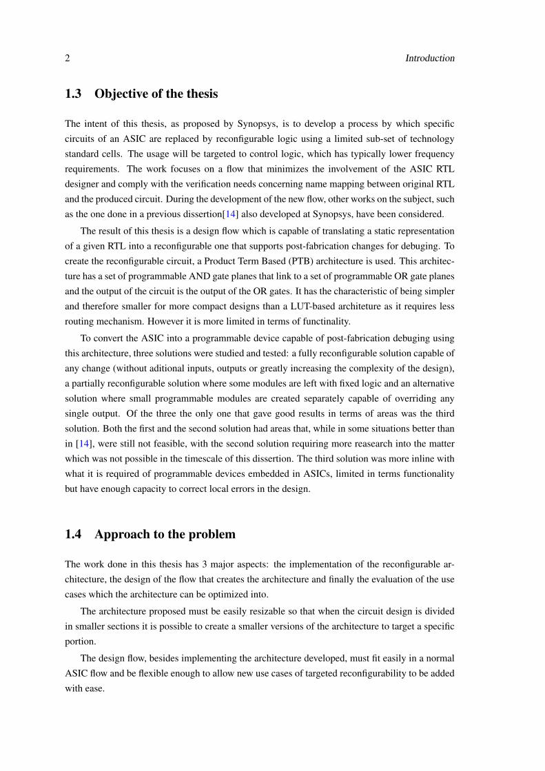
2.2.1 ASIC design flow
An ASIC designer, in standard cell approach, needs to follow a design flow. One common example
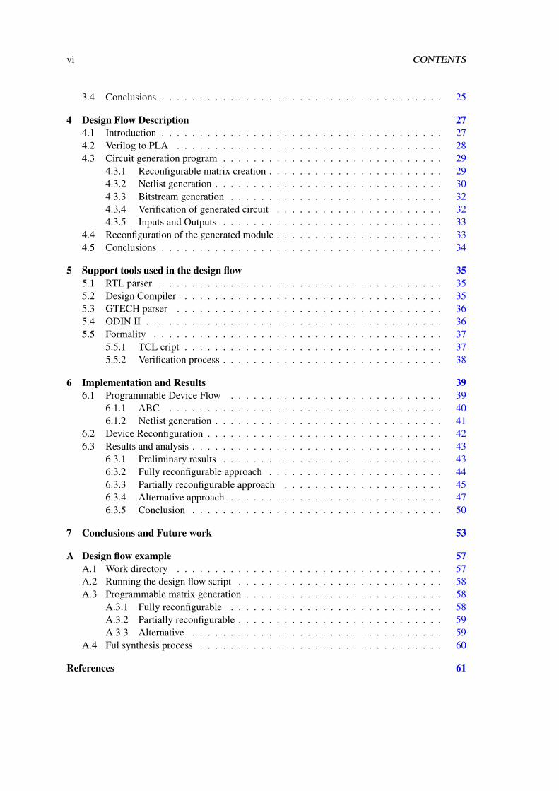
of a design flow can be found in figure 2.1 from [12].
Figure 2.1: ASIC design flow [12]
Overall there are 6 steps composing the ASIC design flow:
• Design entry: The designer will need to provide the description of the circuit at the Register
Transfer Level, in a hardware description language like Verilog, or a schematic entry, for a
standard cell design or full-custom respectively;
2.3 Field Programmable Gate Array (FPGA) 7
• Synthesis: After the HDL (Hardware Description Language) file is synthesized in a synthe-
sis tool, like Synopsys Design Compiler, a netlist is produced as a result with a description
of the logic cells and their connections;
• System partitioning: The netlist that resulted from the previous step is divided into small
parts if the design is large. After those steps, the designer needs to to a post-layout simula-
tion to check if the result from the synthesis is working as intended;
• Floorplanning: The design of the physical part starts with the arrangement of the cells in
the chip;
• Placement: The placement of each block in the chip is determined;
• Routing: The routing that creates the needed interconnections in the chip;
After this, the chip is ready to be produced by providing the tapeout to a foundry.
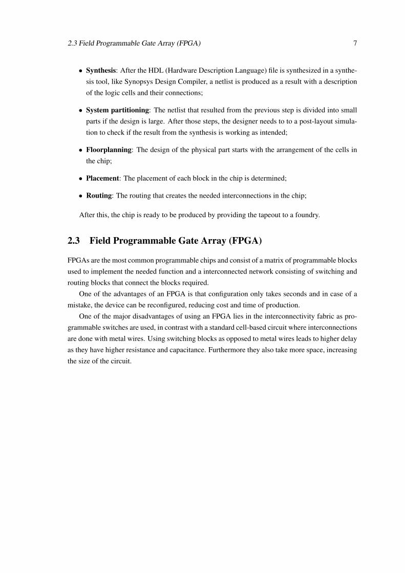
2.3 Field Programmable Gate Array (FPGA)
FPGAs are the most common programmable chips and consist of a matrix of programmable blocks
used to implement the needed function and a interconnected network consisting of switching and
routing blocks that connect the blocks required.
One of the advantages of an FPGA is that configuration only takes seconds and in case of a
mistake, the device can be reconfigured, reducing cost and time of production.
One of the major disadvantages of using an FPGA lies in the interconnectivity fabric as pro-
grammable switches are used, in contrast with a standard cell-based circuit where interconnections
are done with metal wires. Using switching blocks as opposed to metal wires leads to higher delay
as they have higher resistance and capacitance. Furthermore they also take more space, increasing
the size of the circuit.
8 Background Knowledge and Literature Review
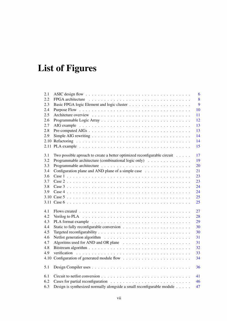
2.3.1 FPGA Architecture
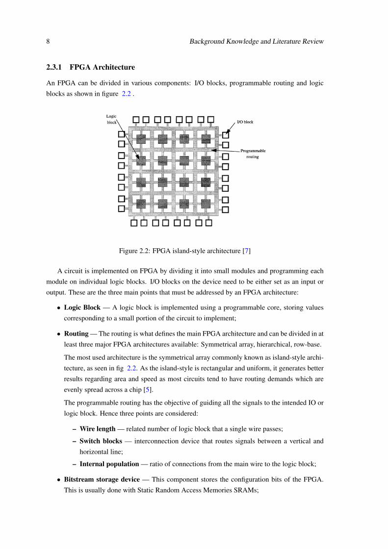
An FPGA can be divided in various components: I/O blocks, programmable routing and logic
blocks as shown in figure 2.2 .
Figure 2.2: FPGA island-style architecture [7]
A circuit is implemented on FPGA by dividing it into small modules and programming each
module on individual logic blocks. I/O blocks on the device need to be either set as an input or
output. These are the three main points that must be addressed by an FPGA architecture:
• Logic Block — A logic block is implemented using a programmable core, storing values
corresponding to a small portion of the circuit to implement;
• Routing — The routing is what defines the main FPGA architecture and can be divided in at
least three major FPGA architectures available: Symmetrical array, hierarchical, row-base.
The most used architecture is the symmetrical array commonly known as island-style archi-
tecture, as seen in fig 2.2. As the island-style is rectangular and uniform, it generates better
results regarding area and speed as most circuits tend to have routing demands which are
evenly spread across a chip [5].
The programmable routing has the objective of guiding all the signals to the intended IO or
logic block. Hence three points are considered:
– Wire length — related number of logic block that a single wire passes;
– Switch blocks — interconnection device that routes signals between a vertical and
horizontal line;
– Internal population — ratio of connections from the main wire to the logic block;
• Bitstream storage device — This component stores the configuration bits of the FPGA.
This is usually done with Static Random Access Memories SRAMs;
2.3 Field Programmable Gate Array (FPGA) 9
2.3.2 Look-up Table
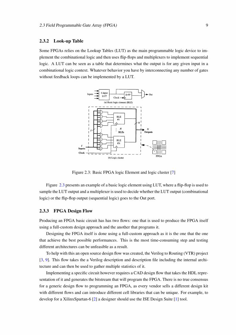
Some FPGAs relies on the Lookup Tables (LUT) as the main programmable logic device to im-
plement the combinational logic and then uses flip-flops and multiplexers to implement sequential
logic. A LUT can be seen as a table that determines what the output is for any given input in a
combinational logic context. Whatever behavior you have by interconnecting any number of gates
without feedback loops can be implemented by a LUT.
Figure 2.3: Basic FPGA logic Element and logic cluster [7]
Figure 2.3 presents an example of a basic logic element using LUT, where a flip-flop is used to
sample the LUT output and a multiplexer is used to decide whether the LUT output (combinational
logic) or the flip-flop output (sequential logic) goes to the Out port.
2.3.3 FPGA Design Flow
Producing an FPGA basic circuit has has two flows: one that is used to produce the FPGA itself
using a full-custom design approach and the another that programs it.
Designing the FPGA itself is done using a full-custom approach as it is the one that the one
that achieve the best possible performances. This is the most time-consuming step and testing
different architectures can be unfeasible as a result.
To help with this an open source design flow was created, the Verilog to Routing (VTR) project
[3, 9]. This flow takes the a Verilog description and description file including the internal archi-
tecture and can then be used to gather multiple statistics of it.
Implementing a specific circuit however requires a CAD design flow that takes the HDL repre-
sentation of it and generates the bitstream that will program the FPGA. There is no true consensus
for a generic design flow to programming an FPGA, as every vendor sells a different design kit
with different flows and can introduce different cell libraries that can be unique. For example, to
develop for a XilinxSpartan-6 [2] a designer should use the ISE Design Suite [1] tool.
10 Background Knowledge and Literature Review
2.4 Standard-Cell-based programmable logic core
Until now most of the microelectronics industry has been dominated by the two methods of circuit
design where the circuit is either completly reconfgurable, like FPGA, or optimized and static
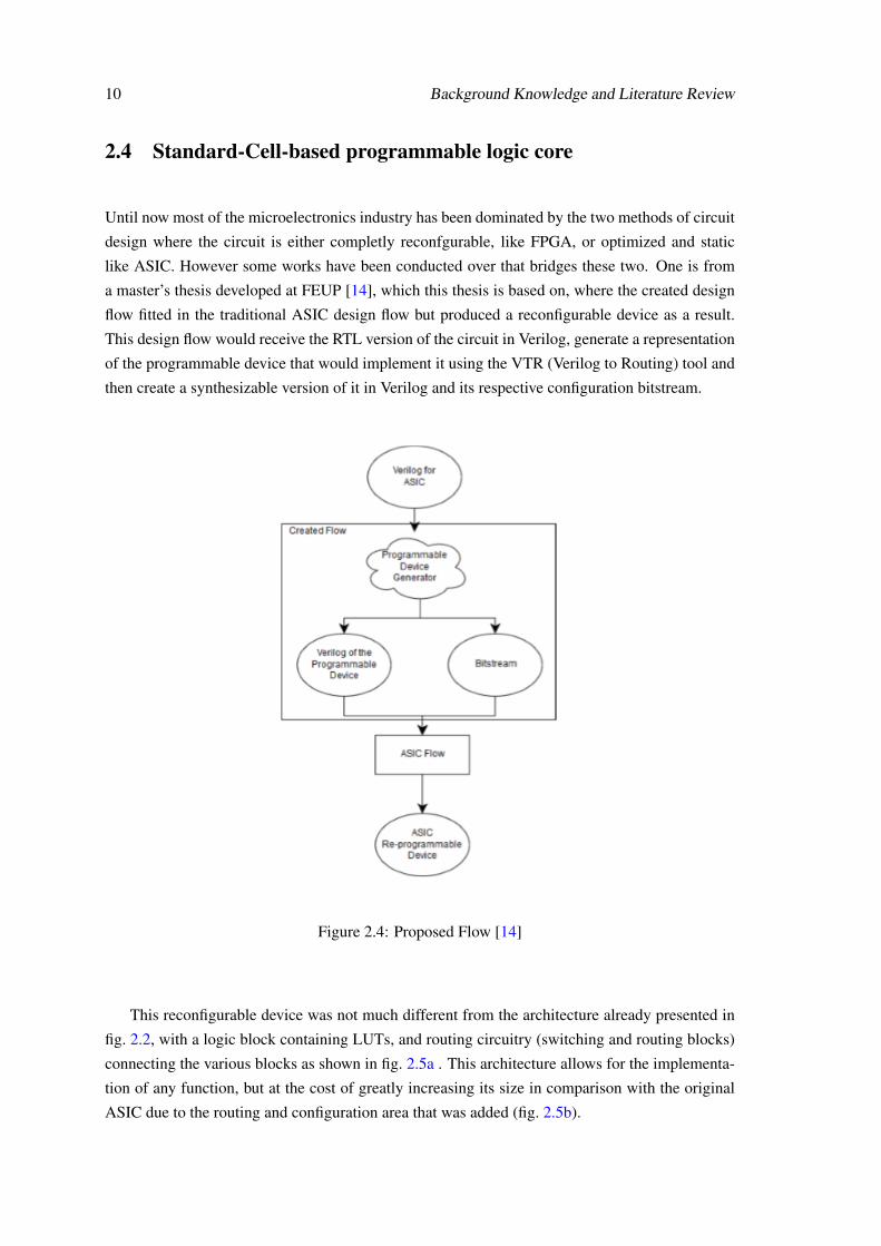
like ASIC. However some works have been conducted over that bridges these two. One is from
a master’s thesis developed at FEUP [14], which this thesis is based on, where the created design
flow fitted in the traditional ASIC design flow but produced a reconfigurable device as a result.
This design flow would receive the RTL version of the circuit in Verilog, generate a representation
of the programmable device that would implement it using the VTR (Verilog to Routing) tool and
then create a synthesizable version of it in Verilog and its respective configuration bitstream.
Figure 2.4: Proposed Flow [14]
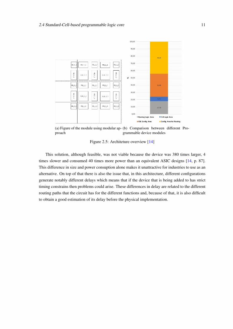
This reconfigurable device was not much different from the architecture already presented in
fig. 2.2, with a logic block containing LUTs, and routing circuitry (switching and routing blocks)
connecting the various blocks as shown in fig. 2.5a . This architecture allows for the implementa-
tion of any function, but at the cost of greatly increasing its size in comparison with the original
ASIC due to the routing and configuration area that was added (fig. 2.5b).
2.4 Standard-Cell-based programmable logic core 11
(a) Figure of the module using modular ap-proach
(b) Comparison between different Pro-grammable device modules
Figure 2.5: Architeture overview [14]
This solution, although feasible, was not viable because the device was 380 times larger, 4
times slower and consumed 40 times more power than an equivalent ASIC designs [14, p. 87].
This difference in size and power consuption alone makes it unattractive for industries to use as an
alternative. On top of that there is also the issue that, in this architecture, different configurations
generate notably different delays which means that if the device that is being added to has strict
timing constrains then problems could arise. These differences in delay are related to the different
routing paths that the circuit has for the different functions and, because of that, it is also difficult
to obtain a good estimation of its delay before the physical implementation.
12 Background Knowledge and Literature Review
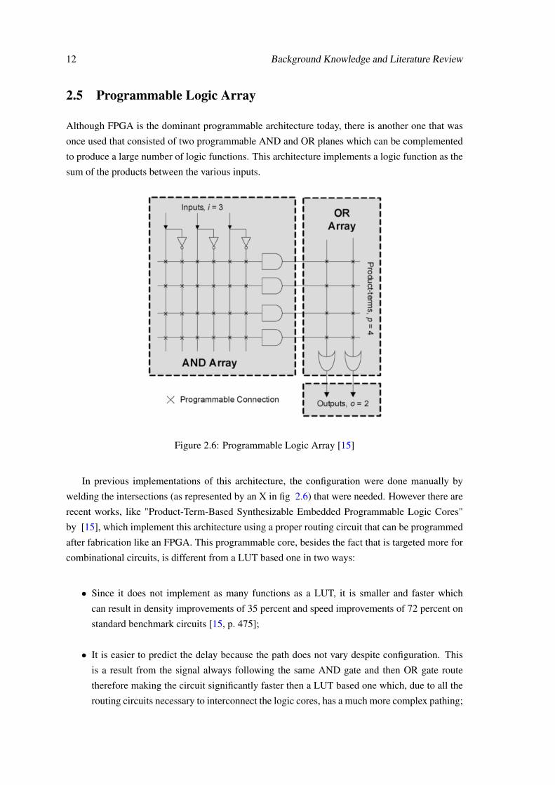
2.5 Programmable Logic Array
Although FPGA is the dominant programmable architecture today, there is another one that was
once used that consisted of two programmable AND and OR planes which can be complemented
to produce a large number of logic functions. This architecture implements a logic function as the
sum of the products between the various inputs.
Figure 2.6: Programmable Logic Array [15]
In previous implementations of this architecture, the configuration were done manually by
welding the intersections (as represented by an X in fig 2.6) that were needed. However there are
recent works, like "Product-Term-Based Synthesizable Embedded Programmable Logic Cores"
by [15], which implement this architecture using a proper routing circuit that can be programmed
after fabrication like an FPGA. This programmable core, besides the fact that is targeted more for
combinational circuits, is different from a LUT based one in two ways:
• Since it does not implement as many functions as a LUT, it is smaller and faster which
can result in density improvements of 35 percent and speed improvements of 72 percent on
standard benchmark circuits [15, p. 475];
• It is easier to predict the delay because the path does not vary despite configuration. This
is a result from the signal always following the same AND gate and then OR gate route
therefore making the circuit significantly faster then a LUT based one which, due to all the
routing circuits necessary to interconnect the logic cores, has a much more complex pathing;
2.5 Programmable Logic Array 13
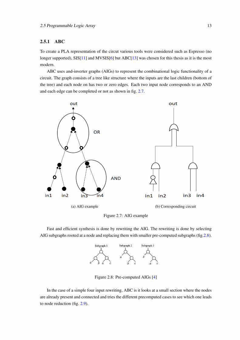
2.5.1 ABC
To create a PLA representation of the circut various tools were considered such as Espresso (no
longer supported), SIS[11] and MVSIS[6] but ABC[13] was chosen for this thesis as it is the most
modern.
ABC uses and-inverter graphs (AIGs) to represent the combinational logic functionality of a
circuit. The graph consists of a tree like structure where the inputs are the last children (bottom of
the tree) and each node on has two or zero edges. Each two input node corresponds to an AND
and each edge can be completed or not as shown in fig. 2.7.
(a) AIG example (b) Corresponding circuit
Figure 2.7: AIG example
Fast and efficient synthesis is done by rewriting the AIG. The rewriting is done by selecting
AIG subgraphs rooted at a node and replacing them with smaller pre-computed subgraphs (fig.2.8).
Figure 2.8: Pre-computed AIGs [4]
In the case of a simple four input rewriting, ABC is it looks at a small section where the nodes
are already present and connected and tries the different precomputed cases to see which one leads
to node reduction (fig. 2.9).
14 Background Knowledge and Literature Review
Figure 2.9: Simple AIG rewriting [4]
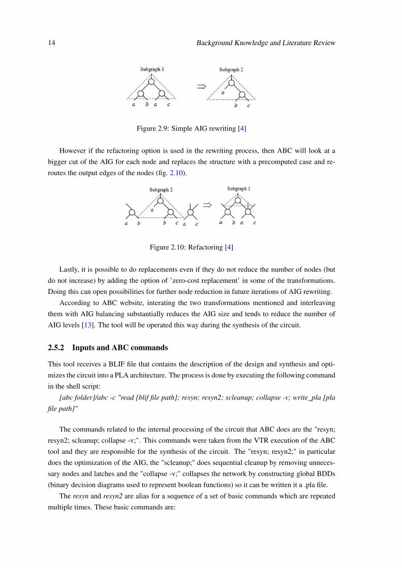
However if the refactoring option is used in the rewriting process, then ABC will look at a
bigger cut of the AIG for each node and replaces the structure with a precomputed case and re-
routes the output edges of the nodes (fig. 2.10).
Figure 2.10: Refactoring [4]
Lastly, it is possible to do replacements even if they do not reduce the number of nodes (but
do not increase) by adding the option of ’zero-cost replacement’ in some of the transformations.
Doing this can open possibilities for further node reduction in future iterations of AIG rewriting.
According to ABC website, interating the two transformations mentioned and interleaving
them with AIG balancing substantially reduces the AIG size and tends to reduce the number of
AIG levels [13]. The tool will be operated this way during the synthesis of the circuit.
2.5.2 Inputs and ABC commands
This tool receives a BLIF file that contains the description of the design and synthesis and opti-
mizes the circuit into a PLA architecture. The process is done by executing the following command
in the shell script:
[abc folder]/abc -c "read [blif file path]; resyn; resyn2; scleanup; collapse -v; write_pla [pla
file path]"
The commands related to the internal processing of the circuit that ABC does are the "resyn;
resyn2; scleanup; collapse -v;". This commands were taken from the VTR execution of the ABC
tool and they are responsible for the synthesis of the circuit. The "resyn; resyn2;" in particular
does the optimization of the AIG, the "scleanup;" does sequential cleanup by removing unneces-
sary nodes and latches and the "collapse -v;" collapses the network by constructing global BDDs
(binary decision diagrams used to represent boolean functions) so it can be written it a .pla file.
The resyn and resyn2 are alias for a sequence of a set of basic commands which are repeated
multiple times. These basic commands are:
2.5 Programmable Logic Array 15
• balance(’b’) — which involves the creation of an equivalent AIG having minimum delay;
• refactor(’r’ or ’rz’) — which attempts to reduce the number of nodes and logic levels by
colapsing and refactoring of logic cones;
• rewrite(’rw’ or ’rwz’) — which attempts to reduce the number of nodes and logic levels
by doing DAG-aware rewriting of the AIG;
In the case of resyn, for example, the sequence goes like "b; rw; rwz; b; rwz; b", which attempts
to perform logic level reduction followed by minimum delay optimization. The rwz and rz com-
mands add the zero-cost replacements option to the refactor and rewrite opperations, meaning that
they reshape the structure even if it does not reduce its size. This reshaping can create logic shar-
ing sections that were not there before, openning possibilites for optimization in future rewriting
iterations. It is possible, however, that using these commands may not be the most efficient way
of processing the network for the PLA, but, nonetheless, they were the basis of how this tools was
used.
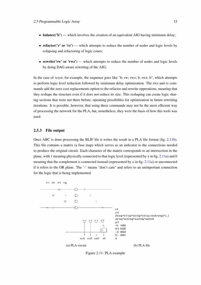
2.5.3 File output
Once ABC is done processing the BLIF file it writes the result in a PLA file format (fig. 2.11b).
This file contains a matrix (a fuse map) which serves as an indicator to the connections needed
to produce the original circuit. Each character of the matrix corresponds to an intersection in the
plane, with 1 meaning physically connected to that logic level (represented by x in fig. 2.11a) and 0
meaning that the complement is connected instead (represented by o in fig. 2.11a) or unconnected
if it refers to the OR plane. The ’-’ means "don’t care" and refers to an unimportant connection
for the logic that is being implemented.
(a) PLA circuit (b) PLA file
Figure 2.11: PLA example
16 Background Knowledge and Literature Review
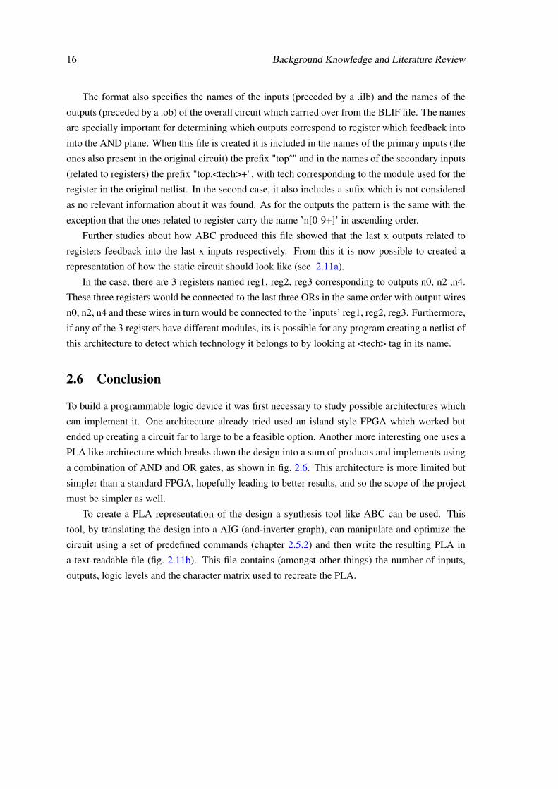
The format also specifies the names of the inputs (preceded by a .ilb) and the names of the
outputs (preceded by a .ob) of the overall circuit which carried over from the BLIF file. The names
are specially important for determining which outputs correspond to register which feedback into
into the AND plane. When this file is created it is included in the names of the primary inputs (the
ones also present in the original circuit) the prefix "topˆ" and in the names of the secondary inputs
(related to registers) the prefix "top.<tech>+", with tech corresponding to the module used for the
register in the original netlist. In the second case, it also includes a sufix which is not considered
as no relevant information about it was found. As for the outputs the pattern is the same with the
exception that the ones related to register carry the name ’n[0-9+]’ in ascending order.
Further studies about how ABC produced this file showed that the last x outputs related to
registers feedback into the last x inputs respectively. From this it is now possible to created a
representation of how the static circuit should look like (see 2.11a).
In the case, there are 3 registers named reg1, reg2, reg3 corresponding to outputs n0, n2 ,n4.
These three registers would be connected to the last three ORs in the same order with output wires
n0, n2, n4 and these wires in turn would be connected to the ’inputs’ reg1, reg2, reg3. Furthermore,
if any of the 3 registers have different modules, its is possible for any program creating a netlist of
this architecture to detect which technology it belongs to by looking at <tech> tag in its name.
2.6 Conclusion
To build a programmable logic device it was first necessary to study possible architectures which
can implement it. One architecture already tried used an island style FPGA which worked but
ended up creating a circuit far to large to be a feasible option. Another more interesting one uses a
PLA like architecture which breaks down the design into a sum of products and implements using
a combination of AND and OR gates, as shown in fig. 2.6. This architecture is more limited but
simpler than a standard FPGA, hopefully leading to better results, and so the scope of the project
must be simpler as well.
To create a PLA representation of the design a synthesis tool like ABC can be used. This
tool, by translating the design into a AIG (and-inverter graph), can manipulate and optimize the
circuit using a set of predefined commands (chapter 2.5.2) and then write the resulting PLA in
a text-readable file (fig. 2.11b). This file contains (amongst other things) the number of inputs,
outputs, logic levels and the character matrix used to recreate the PLA.
Chapter 3
Description of the ProposedProgrammable Architecture
3.1 Introduction
Building the architecture required the creation of the logic circuit that that implements it. However,
simply creating a fully reconfigurable circuit that replaces the original ASIC will just lead to the
same problems as other attempts at replacing reconfigurable with fixed logic such as very high
area due to the added flip-flops for bitstream and the routing circuits [14]. To mitigate the effects
that the added circuitry has on delay, power and area the implementation process must create a
circuit whose programmability is limited to small changes in the logic.
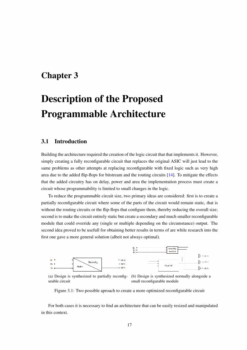
To reduce the programmable circuit size, two primary ideas are considered: first is to create a
partially reconfigurable circuit where some of the parts of the circuit would remain static, that is
without the routing circuits or the flip-flops that configure them, thereby reducing the overall size;
second is to make the circuit entirely static but create a secondary and much smaller reconfigurable
module that could override any (single or multiple depending on the circumstance) output. The
second idea proved to be usefull for obtaining better results in terms of are while research into the
first one gave a more general solution (albeit not always optimal).
(a) Design is synthesized to partially reconfig-urable circuit
(b) Design is synthesized normally alongside asmall reconfigurable module
Figure 3.1: Two possible aproach to create a more optimized reconfigurable circuit
For both cases it is necessary to find an architecture that can be easily resized and manipulated
in this context.
17

18 Description of the Proposed Programmable Architecture
3.2 Architecture description
The implementation done in [14] used LUT as the programable core in combination with a flip-flop
and a multiplexer to form the block that was going to replace the targeted circuit. The first issue
with it is that it implements more than it is necessary (the LUT could perform any combinational
operation) and, therefore, makes the circuit much bigger and slower than accepted. The second
issue is that it is difficult to create a partial reconfigurable version of it because there is no way to
ensure that certain cores will maintain the same functions after a reconfiguration. So, two options
were considered:
• Focus on optimizing the already working architecture by making more efficient (smaller,
faster and less energy consuming) and fixing issues that arose during development but were
not completely or optimally removed;
• Try a different architecture, such as the Product Term Based Architecture which would be
more limited and simpler, but have better prospects in terms of area versus speed and the
impact any sort of reconfiguration will be relatively easy to predict;
In the end option 2 was decided as the best course of action.
3.2 Architecture description 19
3.2.1 Product Term Based Architecture
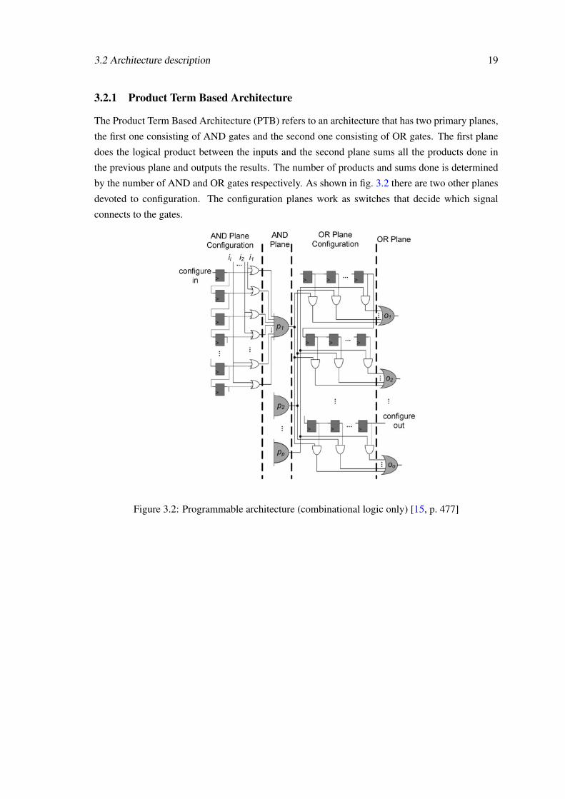
The Product Term Based Architecture (PTB) refers to an architecture that has two primary planes,
the first one consisting of AND gates and the second one consisting of OR gates. The first plane
does the logical product between the inputs and the second plane sums all the products done in
the previous plane and outputs the results. The number of products and sums done is determined
by the number of AND and OR gates respectively. As shown in fig. 3.2 there are two other planes
devoted to configuration. The configuration planes work as switches that decide which signal
connects to the gates.
Figure 3.2: Programmable architecture (combinational logic only) [15, p. 477]
20 Description of the Proposed Programmable Architecture
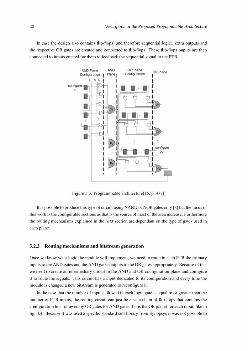
In case the design also contains flip-flops (and therefore sequential logic), extra outputs and
the respective OR gates are created and connected to flip-flops. These flip-flops ouputs are then
connected to inputs created for them to feedback the sequential signal to the PTB.
Figure 3.3: Programmable architecture[15, p. 477]
It is possible to produce this type of circuit using NAND or NOR gates only [8] but the focus of
this work is the configurable sections as that is the source of most of the area increase. Furthermore
the routing mechanisms explained in the next section are dependant on the type of gates used in
each plane.
3.2.2 Routing mechanisms and bitstream generation
Once we know what logic the module will implement, we need to route in each PTB the primary
inputs to the AND gates and the AND gates outputs to the OR gates appropriately. Because of that
we need to create an intermediary circuit in the AND and OR configuration plane and configure
it to route the signals. This circuit has a input dedicated to its configuration and every time the
module is changed a new bitstream is generated to reconfigure it.
In the case that the number of inputs allowed in each logic gate is equal to or greater than the
number of PTB inputs, the routing circuit can just be a scan chain of flip-flops that contains the
configuration bits followed by OR gates (or AND gates if it is the OR plane) for each input, like in
fig. 3.4. Because it was used a specific standard cell library from Synopsys it was not possible to
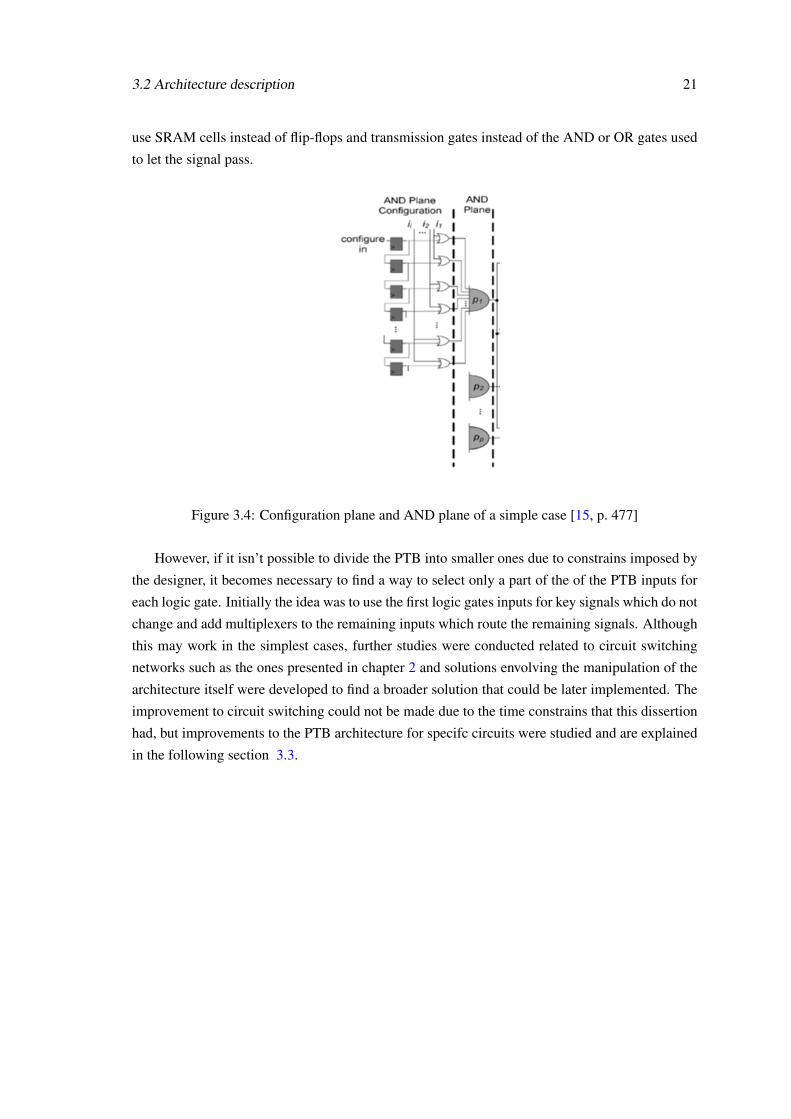
3.2 Architecture description 21
use SRAM cells instead of flip-flops and transmission gates instead of the AND or OR gates used
to let the signal pass.
Figure 3.4: Configuration plane and AND plane of a simple case [15, p. 477]
However, if it isn’t possible to divide the PTB into smaller ones due to constrains imposed by
the designer, it becomes necessary to find a way to select only a part of the of the PTB inputs for
each logic gate. Initially the idea was to use the first logic gates inputs for key signals which do not
change and add multiplexers to the remaining inputs which route the remaining signals. Although
this may work in the simplest cases, further studies were conducted related to circuit switching
networks such as the ones presented in chapter 2 and solutions envolving the manipulation of the
architecture itself were developed to find a broader solution that could be later implemented. The
improvement to circuit switching could not be made due to the time constrains that this dissertion
had, but improvements to the PTB architecture for specifc circuits were studied and are explained
in the following section 3.3.
22 Description of the Proposed Programmable Architecture
3.3 Reconfigurable PTB improvements for specific circuits
One of the issues with reconfigurable circuits is that they impose a cost in terms of area due to
the number of flip-flops necessary to hold the bitstream. Furthermore the reconfigurable circuits
sometimes also has to take into account any unused inputs which could be considered after fabri-
cation. As a result, 5 cases where optimizations could occur in relation to the fully reconfigurable
case and an alternative use of the programmable architecture were studied.
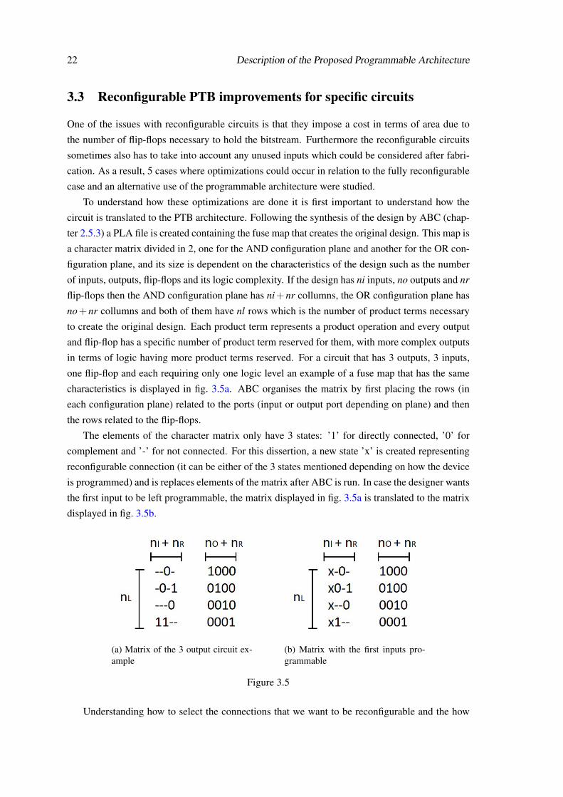
To understand how these optimizations are done it is first important to understand how the
circuit is translated to the PTB architecture. Following the synthesis of the design by ABC (chap-
ter 2.5.3) a PLA file is created containing the fuse map that creates the original design. This map is
a character matrix divided in 2, one for the AND configuration plane and another for the OR con-
figuration plane, and its size is dependent on the characteristics of the design such as the number
of inputs, outputs, flip-flops and its logic complexity. If the design has ni inputs, no outputs and nr
flip-flops then the AND configuration plane has ni+nr collumns, the OR configuration plane has
no+nr collumns and both of them have nl rows which is the number of product terms necessary
to create the original design. Each product term represents a product operation and every output
and flip-flop has a specific number of product term reserved for them, with more complex outputs
in terms of logic having more product terms reserved. For a circuit that has 3 outputs, 3 inputs,
one flip-flop and each requiring only one logic level an example of a fuse map that has the same
characteristics is displayed in fig. 3.5a. ABC organises the matrix by first placing the rows (in
each configuration plane) related to the ports (input or output port depending on plane) and then
the rows related to the flip-flops.
The elements of the character matrix only have 3 states: ’1’ for directly connected, ’0’ for
complement and ’-’ for not connected. For this dissertion, a new state ’x’ is created representing
reconfigurable connection (it can be either of the 3 states mentioned depending on how the device
is programmed) and is replaces elements of the matrix after ABC is run. In case the designer wants
the first input to be left programmable, the matrix displayed in fig. 3.5a is translated to the matrix
displayed in fig. 3.5b.
(a) Matrix of the 3 output circuit ex-ample
(b) Matrix with the first inputs pro-grammable
Figure 3.5
Understanding how to select the connections that we want to be reconfigurable and the how
3.3 Reconfigurable PTB improvements for specific circuits 23
the fuse map is built, by knowing where the inputs, outputs and flip-flop are connected, it is then
possible to define cases where optimizations to the reconfigurable circuit can be made.
3.3.1 Case 1: Only take sequential logic of the design into account
The first case explored was the one where the combinational logic between the inputs and reg-
isters, registers and outputs or between inputs and outputs is removed. This effectively made
the sequential logic (the logic that gets transferred between registers) the only relevant part to be
reconfigurable. To create this scenario it was removed from the reconfigurable section the nLO
product terms that did not feed into the flip-flops and all the rows related to the inputs and outputs
in the AND and OR plane respectively.
(a) Example (b) Resulting optimization
Figure 3.6: Case 1
3.3.2 Case 2: Only take combinational logic of the design into account
The second case relates to the opposite, where the logic between registers is left out and the purely
combinational part of the circuit is left flexible. To create this scenario all connections targeted in
the previous case are removed from the reconfigurable section.
(a) Example (b) Resulting optimization
Figure 3.7: Case 2
3.3.3 Case 3: Module in the design has registers as outputs and its functionalitydoes not change
In case there is a certain module (ex: memory module) whose functionality does not change but its
inputs might then its possible to identify the columns in the second plane that belong to flip-flops
in that module and leave it out of the reconfiguration section and only let the inputs change in the
first plane.
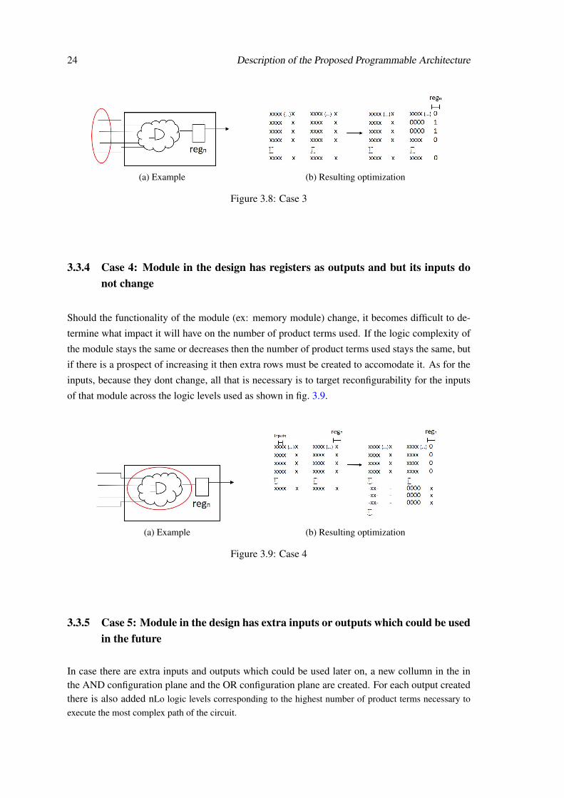
24 Description of the Proposed Programmable Architecture
(a) Example (b) Resulting optimization
Figure 3.8: Case 3
3.3.4 Case 4: Module in the design has registers as outputs and but its inputs donot change
Should the functionality of the module (ex: memory module) change, it becomes difficult to de-
termine what impact it will have on the number of product terms used. If the logic complexity of
the module stays the same or decreases then the number of product terms used stays the same, but
if there is a prospect of increasing it then extra rows must be created to accomodate it. As for the
inputs, because they dont change, all that is necessary is to target reconfigurability for the inputs
of that module across the logic levels used as shown in fig. 3.9.
(a) Example (b) Resulting optimization
Figure 3.9: Case 4
3.3.5 Case 5: Module in the design has extra inputs or outputs which could be usedin the future
In case there are extra inputs and outputs which could be used later on, a new collumn in the inthe AND configuration plane and the OR configuration plane are created. For each output createdthere is also added nLo logic levels corresponding to the highest number of product terms necessary toexecute the most complex path of the circuit.
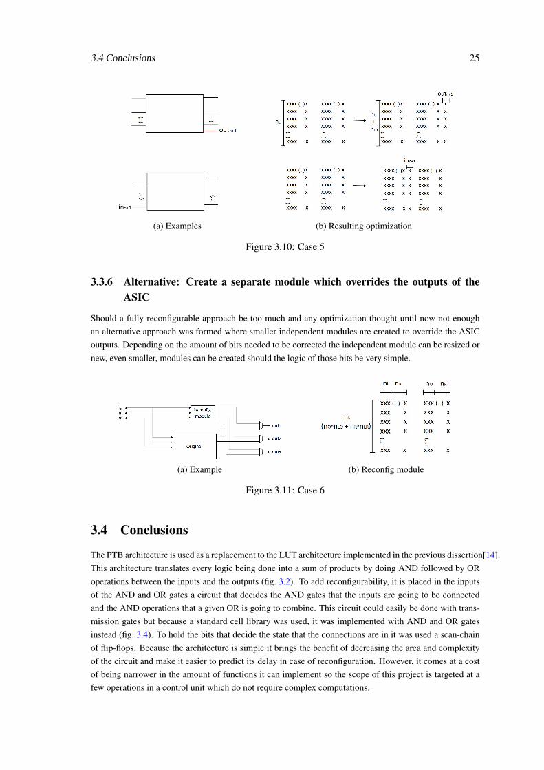
3.4 Conclusions 25
(a) Examples (b) Resulting optimization
Figure 3.10: Case 5
3.3.6 Alternative: Create a separate module which overrides the outputs of theASIC
Should a fully reconfigurable approach be too much and any optimization thought until now not enoughan alternative approach was formed where smaller independent modules are created to override the ASICoutputs. Depending on the amount of bits needed to be corrected the independent module can be resized ornew, even smaller, modules can be created should the logic of those bits be very simple.
(a) Example (b) Reconfig module
Figure 3.11: Case 6
3.4 Conclusions
The PTB architecture is used as a replacement to the LUT architecture implemented in the previous dissertion[14].This architecture translates every logic being done into a sum of products by doing AND followed by ORoperations between the inputs and the outputs (fig. 3.2). To add reconfigurability, it is placed in the inputsof the AND and OR gates a circuit that decides the AND gates that the inputs are going to be connectedand the AND operations that a given OR is going to combine. This circuit could easily be done with trans-mission gates but because a standard cell library was used, it was implemented with AND and OR gatesinstead (fig. 3.4). To hold the bits that decide the state that the connections are in it was used a scan-chainof flip-flops. Because the architecture is simple it brings the benefit of decreasing the area and complexityof the circuit and make it easier to predict its delay in case of reconfiguration. However, it comes at a costof being narrower in the amount of functions it can implement so the scope of this project is targeted at afew operations in a control unit which do not require complex computations.

26 Description of the Proposed Programmable Architecture
During the work of the dissertion this arcitecture is just not implemented by translating the design intoPTB circuit and then making all its componentes programmable (fully reconfigurable approach). Becausethere is the need to reduce the number of flip-flops to the minimum two other approaches to the implemen-tation process were created, one is to create a partially reconfigurable circuit where some of the parts of thecircuit would remain static, that is without the routing circuits or the flip-flops that configure them, therebyreducing the overall size and another is to make the circuit entirely static but create a secondary and muchsmaller reconfigurable module that could override any (single or multiple depending on the circumstance)output. These three approaches will eventually be covered in chapter 6.3
Chapter 4
Design Flow Description
4.1 Introduction
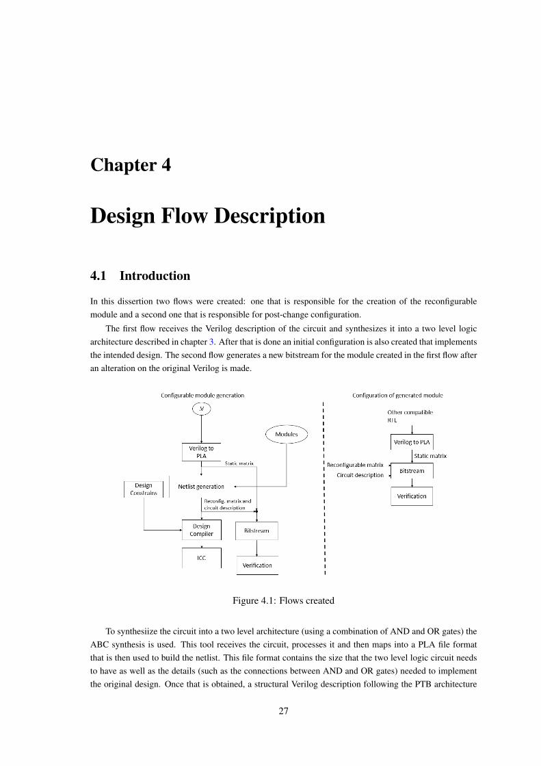
In this dissertion two flows were created: one that is responsible for the creation of the reconfigurablemodule and a second one that is responsible for post-change configuration.
The first flow receives the Verilog description of the circuit and synthesizes it into a two level logicarchitecture described in chapter 3. After that is done an initial configuration is also created that implementsthe intended design. The second flow generates a new bitstream for the module created in the first flow afteran alteration on the original Verilog is made.
Figure 4.1: Flows created
To synthesiize the circuit into a two level architecture (using a combination of AND and OR gates) theABC synthesis is used. This tool receives the circuit, processes it and then maps into a PLA file formatthat is then used to build the netlist. This file format contains the size that the two level logic circuit needsto have as well as the details (such as the connections between AND and OR gates) needed to implementthe original design. Once that is obtained, a structural Verilog description following the PTB architecture
27
28 Design Flow Description
is created, serving as the netlist. This architecture will contain routing mechanisms, such as the scan chainas shown in the example 3.2, that decide which input connects to certain AND gates and will be thetarget of the bitstream that is generated. Finaly, after we have a valid Verilog description, the flow willcontinue similarly to the ASIC with the synthesis of the device being done using the Design Compiler andthe physical implementation using IC Compiler, both provided by Synopsys.
4.2 Verilog to PLA
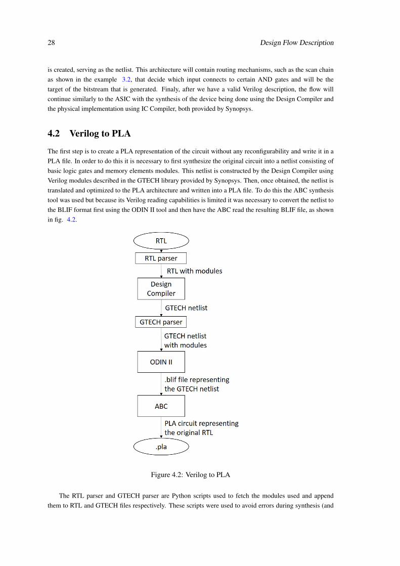
The first step is to create a PLA representation of the circuit without any reconfigurability and write it in aPLA file. In order to do this it is necessary to first synthesize the original circuit into a netlist consisting ofbasic logic gates and memory elements modules. This netlist is constructed by the Design Compiler usingVerilog modules described in the GTECH library provided by Synopsys. Then, once obtained, the netlist istranslated and optimized to the PLA architecture and written into a PLA file. To do this the ABC synthesistool was used but because its Verilog reading capabilities is limited it was necessary to convert the netlist tothe BLIF format first using the ODIN II tool and then have the ABC read the resulting BLIF file, as shownin fig. 4.2.
Figure 4.2: Verilog to PLA
The RTL parser and GTECH parser are Python scripts used to fetch the modules used and appendthem to RTL and GTECH files respectively. These scripts were used to avoid errors during synthesis (and

4.3 Circuit generation program 29
later during verification) in case the tools could find the modules referenced within the main project. TheGTECH parser is the same python script used in Valverde’s dissertion for the same purpose.
Table 4.1: Inputs and outputs of the Verilog to PLA phase
Inputs OutputsRTL to be synthesized GTECH netlist
BLIF file translated from the netlistPLA representation of the design
4.3 Circuit generation program
After the PLA file is created the next step is to interpret it and generate a Verilog netlist from it. For thispurpose, a python program was created, which reads the PLA file, create an abstract representation of areconfigurable PLA in the form of a character matrix and finally writes the Verilog netlist representing thereconfigurable circuit.
4.3.1 Reconfigurable matrix creation
The PLA file contains input and output names as well as a character matrix defining the internal structureof the PLA. This matrix can be divided in 2, one for the AND configuration plane and one for the ORconfiguration plane, and it tells where the inputs and outputs are going to be placed and how the logic gatesare connected internally.
Figure 4.3: PLA format example
This matrix represents the circuit in a static PTB, that is without scan-chain to configure it or any routingor input selection machanisms, and it is through the manipulation of this matrix that the optimization andeffiency of the circuit can be achieved.
The reconfigurable circuit can be optimized by narrowing the scope at which the configuration will beapplied and the efficiency can be improved by eliminating redundant configurations. Both of these weredone by selecting positions in the matrix and replacing the character in that position with the character ’x’ asa way for the program that generates the circuit to, later on, recognize which connections are reconfigurable
30 Design Flow Description
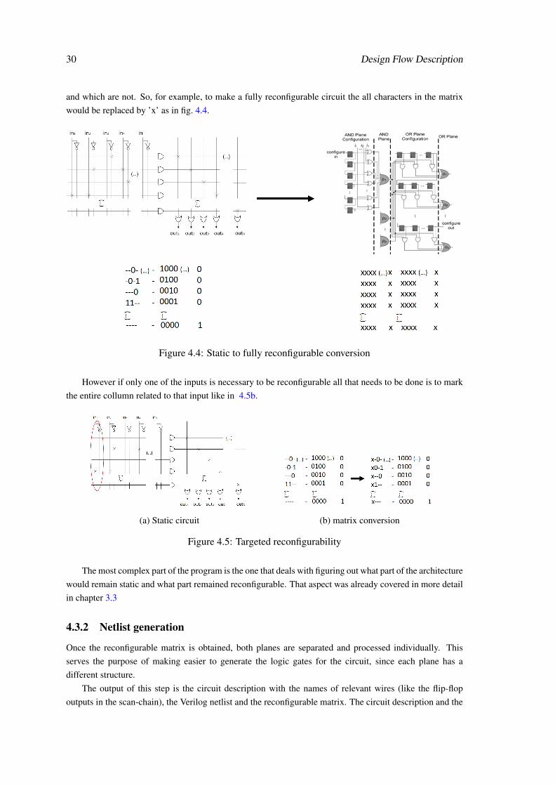
and which are not. So, for example, to make a fully reconfigurable circuit the all characters in the matrixwould be replaced by ’x’ as in fig. 4.4.
Figure 4.4: Static to fully reconfigurable conversion
However if only one of the inputs is necessary to be reconfigurable all that needs to be done is to markthe entire collumn related to that input like in 4.5b.
(a) Static circuit (b) matrix conversion
Figure 4.5: Targeted reconfigurability
The most complex part of the program is the one that deals with figuring out what part of the architecturewould remain static and what part remained reconfigurable. That aspect was already covered in more detailin chapter 3.3
4.3.2 Netlist generation
Once the reconfigurable matrix is obtained, both planes are separated and processed individually. Thisserves the purpose of making easier to generate the logic gates for the circuit, since each plane has adifferent structure.
The output of this step is the circuit description with the names of relevant wires (like the flip-flopoutputs in the scan-chain), the Verilog netlist and the reconfigurable matrix. The circuit description and the
4.3 Circuit generation program 31
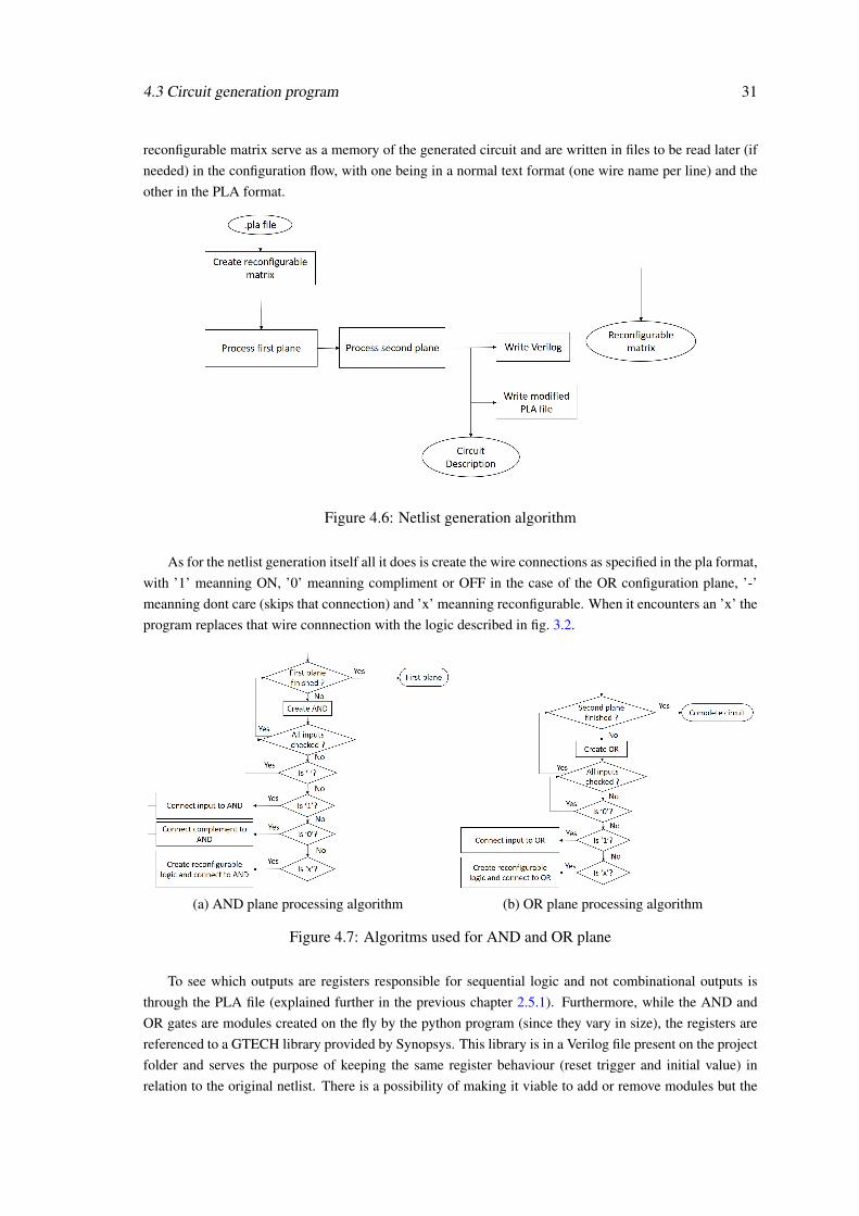
reconfigurable matrix serve as a memory of the generated circuit and are written in files to be read later (ifneeded) in the configuration flow, with one being in a normal text format (one wire name per line) and theother in the PLA format.
Figure 4.6: Netlist generation algorithm
As for the netlist generation itself all it does is create the wire connections as specified in the pla format,with ’1’ meanning ON, ’0’ meanning compliment or OFF in the case of the OR configuration plane, ’-’meanning dont care (skips that connection) and ’x’ meanning reconfigurable. When it encounters an ’x’ theprogram replaces that wire connnection with the logic described in fig. 3.2.
(a) AND plane processing algorithm (b) OR plane processing algorithm
Figure 4.7: Algoritms used for AND and OR plane
To see which outputs are registers responsible for sequential logic and not combinational outputs isthrough the PLA file (explained further in the previous chapter 2.5.1). Furthermore, while the AND andOR gates are modules created on the fly by the python program (since they vary in size), the registers arereferenced to a GTECH library provided by Synopsys. This library is in a Verilog file present on the projectfolder and serves the purpose of keeping the same register behaviour (reset trigger and initial value) inrelation to the original netlist. There is a possibility of making it viable to add or remove modules but the
32 Design Flow Description
program responsible for the netlist foscused only on the GTECH modules provided as it was easier for theexamples tested.
4.3.3 Bitstream generation
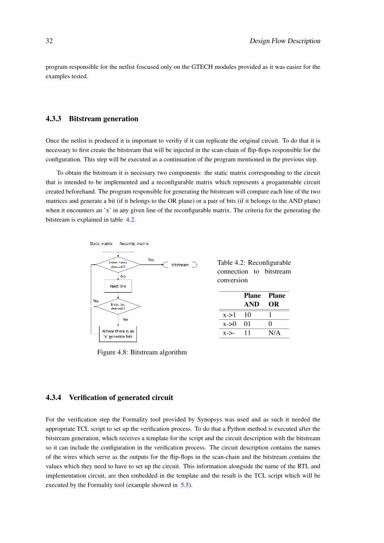
Once the netlist is produced it is important to verifiy if it can replicate the original circuit. To do that it isnecessary to first create the bitstream that will be injected in the scan-chain of flip-flops responsible for theconfiguration. This step will be executed as a continuation of the program mentioned in the previous step.
To obtain the bitstream it is necessary two components: the static matrix corresponding to the circuitthat is intended to be implemented and a reconfigurable matrix which represents a progammable circuitcreated beforehand. The program responsible for generating the bitstream will compare each line of the twomatrices and generate a bit (if it belongs to the OR plane) or a pair of bits (if it belongs to the AND plane)when it encounters an ’x’ in any given line of the reconfigurable matrix. The criteria for the generating thebitstream is explained in table 4.2.
Figure 4.8: Bitstream algorithm
Table 4.2: Reconfigurableconnection to bitstreamconversion
Plane PlaneAND OR
x->1 10 1x->0 01 0x->- 11 N/A
4.3.4 Verification of generated circuit
For the verification step the Formality tool provided by Synopsys was used and as such it needed theappropriate TCL script to set up the verification process. To do that a Python method is executed after thebitstream generation, which receives a template for the script and the circuit description with the bitstreamso it can include the configuration in the verification process. The circuit description contains the namesof the wires which serve as the outputs for the flip-flops in the scan-chain and the bitstream contains thevalues which they need to have to set up the circuit. This information alongside the name of the RTL andimplementation circuit, are then embedded in the template and the result is the TCL script which will beexecuted by the Formality tool (example showed in 5.5).
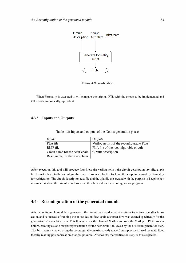
4.4 Reconfiguration of the generated module 33
Figure 4.9: verification
When Formality is executed it will compare the original RTL with the circuit to be implemented andtell if both are logically equivalent.
4.3.5 Inputs and Outputs
Table 4.3: Inputs and outputs of the Netlist generation phase
Inputs OutputsPLA file Verilog netlist of the reconfigurable PLABLIF file PLA file of the reconfigurable circuitClock name for the scan-chain Circuit descriptionReset name for the scan-chain
After execution this tool will produce four files: the verilog netlist, the circuit description text file, a .plafile format related to the reconfigurable matrix produced by this tool and the script to be used by Formalityfor verification. The circuit description text file and the .pla file are created with the purpose of keeping keyinformation about the circuit stored so it can then be used for the reconfiguration program.
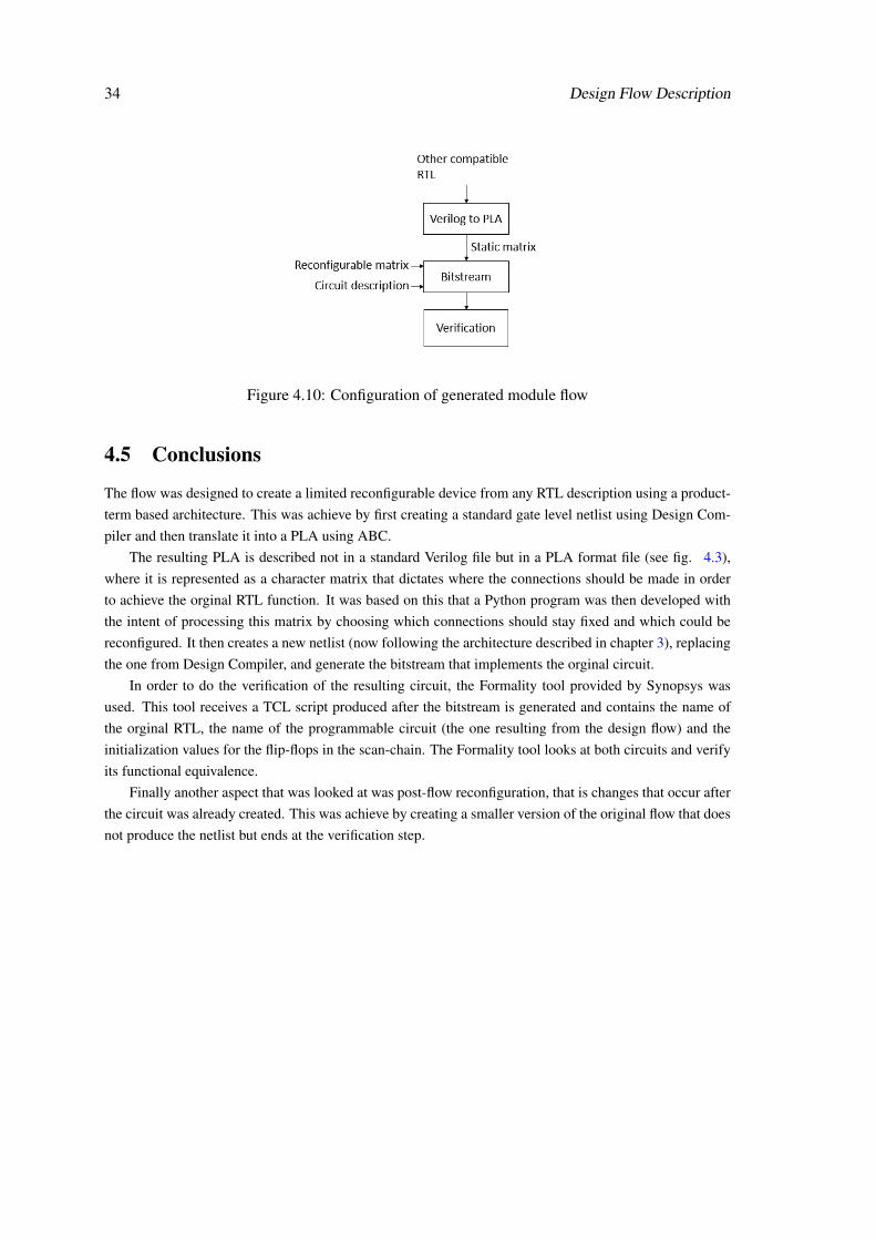
4.4 Reconfiguration of the generated module
After a configurable module is generated, the circuit may need small alterations to its function after fabri-cation and so instead of running the entire design flow again a shorter flow was created specifically for thegeneration of a new bitstream. This flow receives the changed Verilog and runs the Verilog to PLA processbefore, creating a static matrix representation for the new circuit, followed by the bitstream generation step.This bitstream is created using the reconfigurable matrix already made from a previous run of the main flow,thereby making post fabrication changes possible. Afterwards, the verification step, runs as expected.
34 Design Flow Description
Figure 4.10: Configuration of generated module flow
4.5 Conclusions
The flow was designed to create a limited reconfigurable device from any RTL description using a product-term based architecture. This was achieve by first creating a standard gate level netlist using Design Com-piler and then translate it into a PLA using ABC.
The resulting PLA is described not in a standard Verilog file but in a PLA format file (see fig. 4.3),where it is represented as a character matrix that dictates where the connections should be made in orderto achieve the orginal RTL function. It was based on this that a Python program was then developed withthe intent of processing this matrix by choosing which connections should stay fixed and which could bereconfigured. It then creates a new netlist (now following the architecture described in chapter 3), replacingthe one from Design Compiler, and generate the bitstream that implements the orginal circuit.
In order to do the verification of the resulting circuit, the Formality tool provided by Synopsys wasused. This tool receives a TCL script produced after the bitstream is generated and contains the name ofthe orginal RTL, the name of the programmable circuit (the one resulting from the design flow) and theinitialization values for the flip-flops in the scan-chain. The Formality tool looks at both circuits and verifyits functional equivalence.
Finally another aspect that was looked at was post-flow reconfiguration, that is changes that occur afterthe circuit was already created. This was achieve by creating a smaller version of the original flow that doesnot produce the netlist but ends at the verification step.
Chapter 5
Support tools used in the design flow
5.1 RTL parser
Some models provided by Synopsys for experimentation contained includes and other models not declaredwithin the RTL file and as such it needed to be referenced in the Design Compiler script for synthesis.However because the problem persisted in other tools (such as Formality in the verification step) and inorder to fix that issue it required knowledge in how to do the scripts for these tools, it was decided insteadto develop a Python script that searched all the modules and appended them to the orginal RTL. This RTLwould then be copied to a folder within the Design Compiler working directory for synthesis and later onfor reference in the verification process.
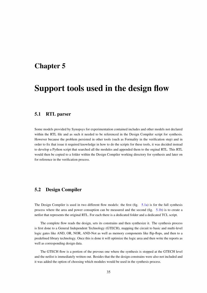
5.2 Design Compiler
The Design Compiler is used in two different flow models: the first (fig. 5.1a) is for the full synthesisprocess where the area and power consuption can be measured and the second (fig. 5.1b) is to create anetlist that represents the original RTL. For each there is a dedicated folder and a dedicated TCL script.
The complete flow reads the design, sets its constrains and then synthesize it. The synthesis processis first done to a General Independent Technology (GTECH), mapping the circuit to basic and multi-levellogic gates like AND, OR, NOR, AND-Not as well as memory components like flip-flops, and then to apredefined library technology. Once this is done it will optimize the logic area and then write the reports aswell as corresponding design data.
The GTECH flow is a portion of the prevous one where the synthesis is stopped at the GTECH leveland the netlist is immediately written out. Besides that the the design constrains were also not included andit was added the option of choosing which modules would be used in the synthesis process.
35
36 Support tools used in the design flow
(a) Complete synthesis (b) GTECH synthesis
Figure 5.1: Design Compiler uses
5.3 GTECH parser
Once the GTECH netlist is obtained from the Design Compiler a similar process to the RTL parser is donefor ODINII, where the GTECH modules referenced but not declared were appended to the end of the netlist.The result is then copied to a directory for ODINII to process.
The script used for this step was the same as the one used by Valverde in his thesis [14, p. 38].
5.4 ODIN II
Following the netlist generation by the Design Compiler it is then necessary to use ABC for the PLAconversion. However because ABC can not read the verilog directly it needs a blif converter first. For thatpurpose ODIN II was used as an intermediary verilog to blif converter by executing it with the following command:
[ODIN II folder]/odin.exe -V [target verilog file path] -o [resulting blif file path]
One of the most important construct a mapped BLIF file relates are flip-flops. To declare one the BLIFfile should include the .latch model as displayed:
.latch [input] [output] [type] [control] [init-val]
As can be seen only inputs, outputs and clock signal are declared but not the reset. This is because theBLIF file cannot express asynchronous reset so a signal must be predefined to all flip-flops related to thesequential part of the architecture before the flow is run.
5.5 Formality 37
5.5 Formality
To verify if the circuit generated is equivalent to the original RTL a verification tool had to be used. At firstit was considered using a custom-made testbench, however since Synopsys provided the Formality tool forverification and testbenchs for large projects can end up being flawed and/or too slow, the latter option waschosen instead.
5.5.1 TCL cript
When Formality runs it does so with the aid of a TCL script. This script contains declaration and initializa-tion of basic internal variables used by the tool,such as the the design name and the RTL path, as well thesequence of commands to be executed. For example the basic script should look like this:
#VARIABLE DECLARATIONS#set design [top level design name]set rtl_path .̈.rtl_v¨set rtl_list $̈{rtl_path}convert_to_gtech¨ (This variable is the path to the rtl which was/will be synthesizedto a GTECH netlist by Design Compiler;see 5.1 for clarification)
#SETUP INFORMATION#set_svf .$design.svf"report_guidance -to ./${design}_report_guidance.svf"
#REFERENCE DESIGN#read_verilog -r "$rtl_list" (Sets the container r to the original RTL)set_top r:WORK${design}
#IMPLEMENTATION DESIGN#read_verilog -i "[path of the synthesized design]" (Sets the container i to the synthesized design)set_top i:WORK${design}
#RUN MATCH#match
#RUN VERIFY#verifyreport_failling_points
exit
After it starts the verification process the Formality will not guess which state the flip-flops in the scan-chain will be in and will assume it is part of the internal logic. As such it needed to be included in the scriptwhich value theses flip-flops would take by giving its wire output the ’1’ or ’0’ value. This was done bywriting the following command for each wire before the "RUN MATCH" phase is run:
set_constant i:WORK${design}[wire name] [bit value] -type net

38 Support tools used in the design flow
5.5.2 Verification process
The verification process itself consists of comparing the combinational (by analysing the immediate resultfrom a set of inputs) and sequential behaviour (by analysing the evolution of the internal state) betweenthe two verilogs and then indicating ,if there is something wrong, which outputs and registers are not beingproperly implemented.
Chapter 6
Implementation and Results
In the previous chapter the tools and methods used to implement this solution were explained. First, theprogrammable architecture that produces the intended logic was explained in chapter 3. This architectureis based on a Programmable Logic Array architecture that replaces the physical connections with a config-urable circuit. Then in chapter 4 a design flow was described that receives a RTL description of the designwritten in Verilog and creates a netlist whose circuit follows that architecture. The design flow requiredcustom-made tools (mostly Python programs and Bash scripts) as well as external tools such as SynopsysDesign Compiler, for full and partial synthesis, and ABC, for the PLA creation, both of which were de-scribed in chapter 5. Once everything was set-up, the tool flow were used to create the device, verify itand then obtain information about the area, timing and power. This chapter will describe in more detail thesteps taken to implement the flow and analysis of results.
6.1 Programmable Device Flow
The approach done to create the programmable device was to design a process by which the designer givesthe RTL to implement and then the netlist is created. This netlist is then copied to the folder where thefull synthesis and pyhsical implementation of the device occurs. To do this, a Bash script was created thatexecutes the steps in the following order:
#DEFINE CLOCK AND RESET NAMES FOR SCAN-CHAIN FLIP-FLOPS#se restName = "pgr_clk"set clkName = "pgr_rst"
#PARSE VERILOG#python parseVerilog.py rtl_v/ ${projectFile}.v [directory1]/convert_to_gtech.v
#RUN DESIGN COMPILER#dc_shell -f gtech_dc.tcl
#PARSE GTECH NETLIST#python2 pyparse_hier.py [directory1]/hier.tmp gtech_lib.pg.v [directory2]/gtech_parse.lib
#EXECUTE ODIN II#odin_II.exe -V [directory1]/${projectFile}_gtech.v -o [directory2]/${projectFile}.blif
39
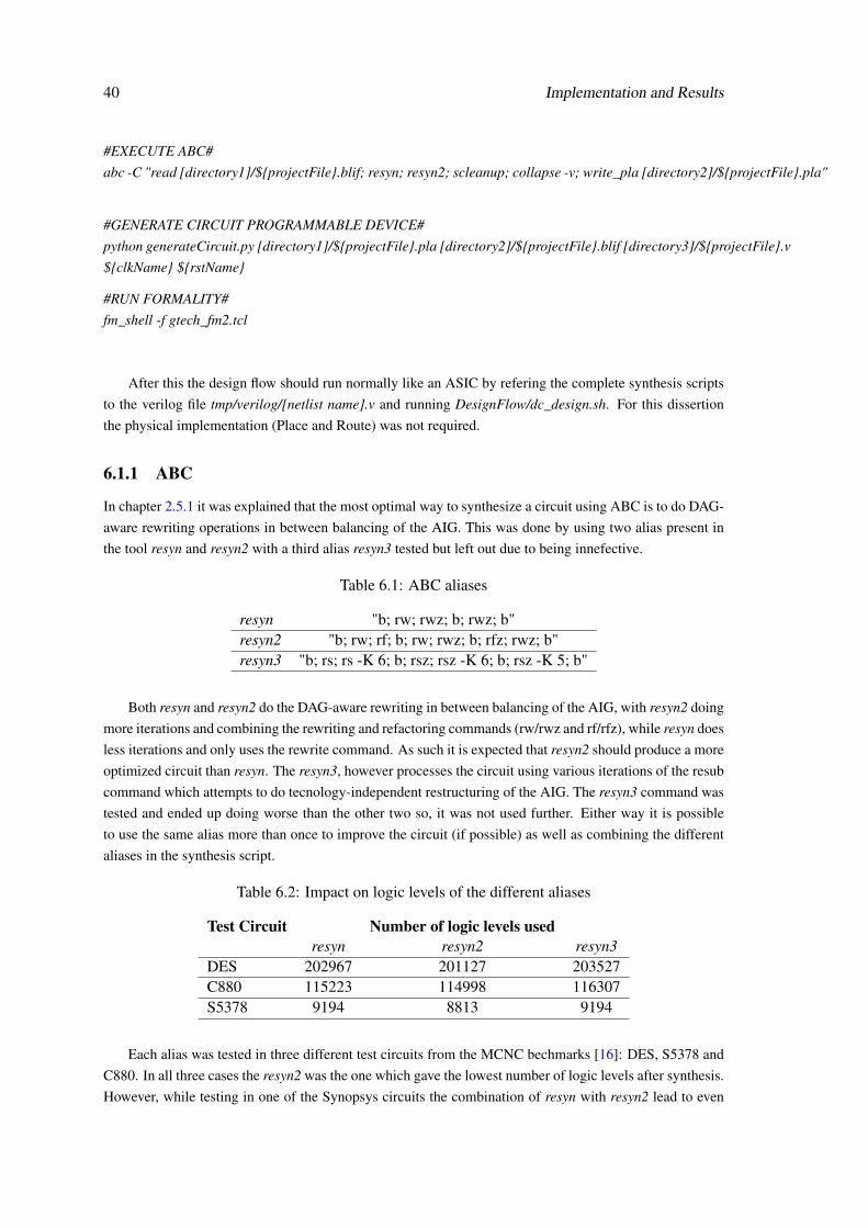
40 Implementation and Results
#EXECUTE ABC#abc -C "read [directory1]/${projectFile}.blif; resyn; resyn2; scleanup; collapse -v; write_pla [directory2]/${projectFile}.pla"
#GENERATE CIRCUIT PROGRAMMABLE DEVICE#python generateCircuit.py [directory1]/${projectFile}.pla [directory2]/${projectFile}.blif [directory3]/${projectFile}.v${clkName} ${rstName}
#RUN FORMALITY#fm_shell -f gtech_fm2.tcl
After this the design flow should run normally like an ASIC by refering the complete synthesis scriptsto the verilog file tmp/verilog/[netlist name].v and running DesignFlow/dc_design.sh. For this dissertionthe physical implementation (Place and Route) was not required.
6.1.1 ABC
In chapter 2.5.1 it was explained that the most optimal way to synthesize a circuit using ABC is to do DAG-aware rewriting operations in between balancing of the AIG. This was done by using two alias present inthe tool resyn and resyn2 with a third alias resyn3 tested but left out due to being innefective.
Table 6.1: ABC aliases
resyn "b; rw; rwz; b; rwz; b"resyn2 "b; rw; rf; b; rw; rwz; b; rfz; rwz; b"resyn3 "b; rs; rs -K 6; b; rsz; rsz -K 6; b; rsz -K 5; b"
Both resyn and resyn2 do the DAG-aware rewriting in between balancing of the AIG, with resyn2 doingmore iterations and combining the rewriting and refactoring commands (rw/rwz and rf/rfz), while resyn doesless iterations and only uses the rewrite command. As such it is expected that resyn2 should produce a moreoptimized circuit than resyn. The resyn3, however processes the circuit using various iterations of the resubcommand which attempts to do tecnology-independent restructuring of the AIG. The resyn3 command wastested and ended up doing worse than the other two so, it was not used further. Either way it is possibleto use the same alias more than once to improve the circuit (if possible) as well as combining the differentaliases in the synthesis script.
Table 6.2: Impact on logic levels of the different aliases
Test Circuit Number of logic levels usedresyn resyn2 resyn3
DES 202967 201127 203527C880 115223 114998 116307S5378 9194 8813 9194
Each alias was tested in three different test circuits from the MCNC bechmarks [16]: DES, S5378 andC880. In all three cases the resyn2 was the one which gave the lowest number of logic levels after synthesis.However, while testing in one of the Synopsys circuits the combination of resyn with resyn2 lead to even
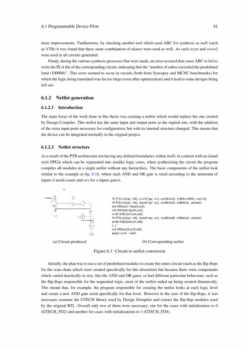
6.1 Programmable Device Flow 41
more improvements. Furthermore, by checking another tool which used ABC for synthesis as well (suchas VTR) it was found that these same combination of aliases were used as well. As such resyn and resyn2were used in all circuits generated.
Finaly, during the various synthesis processes that were made, an error occured that cause ABC to fail towrite the PLA file of the corresponding circuit, indicating that the "number of cubes exceeded the predefinedlimit (100000)". This error seemed to occur in circuits (both from Synospsy and MCNC benchmarks) forwhich the logic being translated was far too large (even after optimization) and it lead to some designs beingleft out.
6.1.2 Netlist generation
6.1.2.1 Introduction
The main focus of the work done in this thesis was creating a netlist which would replace the one createdby Design Compiler. This netlist has the same input and output ports as the orginal one, with the additionof the extra input ports necessary for configuration, but with its internal structure changed. This means thatthe device can be integrated normally in the original project.
6.1.2.2 Netlist structure
As a result of the PTB architecture not having any defined boundaries within itself, in contrast with an islandstyle FPGA which can be segmented into smaller logic cores, when synthesizing the circuit the programcompiles all modules in a single netlist without any hierarchies. The basic components of the netlist looksimilar to the example in fig. 6.1b, where each AND and OR gate is sized according to the ammount ofinputs it needs (andx and orx for x inputs gates).
(a) Circuit produced (b) Corresponding netlist
Figure 6.1: Circuit to netlist conversion
Initially, the plan was to use a set of predefined modules to create the entire circuit (such as the flip-flopsfor the scan-chain which were created specifically for this dissertion) but because there were componentswhich varied drastically in size, like the AND and OR gates, or had different particular behaviour, such asthe flip-flops responsible for the sequential logic, most of the netlist ended up being created dinamically.This meant that, for example, the program responsible for creating the netlist looks at each logic leveland create a new AND gate sized specifically for that level. However in the case of the flip-flops, it wasnecessary examine the GTECH library used by Design Dompiler and extract the flip-flop modules usedby the original RTL. Overall only two of them were necessary, one for the cases with initialization to 0(GTECH_FD2) and another for cases with initializations to 1 (GTECH_FD4).
42 Implementation and Results
6.1.2.3 Design issues
One of the problems encountered when synthesising designs from Synopsys was that the clocks and resetsof flip-flops were not always consistent. This meant that instead of having the clock and reset name bepassed as an argument for the script, a method was developed within the netlist program that could searchand find their soure. For this both the BLIF file generated by ODIN II and the GTECH netlist were essentialto fix the problem.
When it came to finding the clock all it needed to do was to look at the BLIF file and for every flip-flopdeclared (in the name of latch for this format) there was the corresponding clock signal [10]:
.latch <input> <output> [<type> <clk_name>] [<init-val>]
However for the reset signal it was necessary to search for the entire GTECH netlist to find the reset signalfor every flip-flop. Still for the cases where either the clocks or the resets had internal logic which generatedthem the issue still remained but because they demanded so much resources and effort to find a solution(such as searching the entire logic within the GETCH netlist and porting to the new netlist) it was eventuallyleft out for future work.
6.2 Device Reconfiguration
In case a modification is made to the design, it becomes necessary to verify if the programmable device iscan be used to implement it. For that a new PLA matrix is genererated for the modified circuit and matchedwith the one corresponding to the programmable module. To do that, a Python program was developed thattakes both matrices, generate the bitstream necessary to implement the modified design and run Formalityfor formal verification. If either the bitstream generation failed (due to incompatibilities in size or logic outof reach) or the procedure failed, then the design and the circuit are deemed incompatible. The script usedto implement this process assumes the modified RTL to be in the same directory as the orignal and the samename with a _modi f ed attached at the end.
#PARSE VERILOG#python parseVerilog.py rtl_v/ ${projectFile}_modified.v [directory1]/convert_to_gtech.v
#RUN DESIGN COMPILER#dc_shell -f gtech_dc.tcl
#PARSE GTECH NETLIST#python2 pyparse_hier.py [directory1]/hier.tmp gtech_lib.pg.v [directory2]/gtech_parse.lib
#EXECUTE ODIN II#odin_II.exe -V [directory1]/${projectFile}_modified_gtech.v -o [directory2]/${projectFile}_modified.blif
#EXECUTE ABC#abc -C "read [directory1]/${projectFile}_modified.blif; resyn; resyn2; scleanup; collapse -v; write_pla[directory2]/${projectFile}_modified.pla"
#GENERATE BITSTREAM#python generateBitstream.py [directory1]/${projectFile}_modified.pla [directory2]/${projectFile}.pla
#RUN FORMALITY#fm_shell -f gtech_fm2.tcl
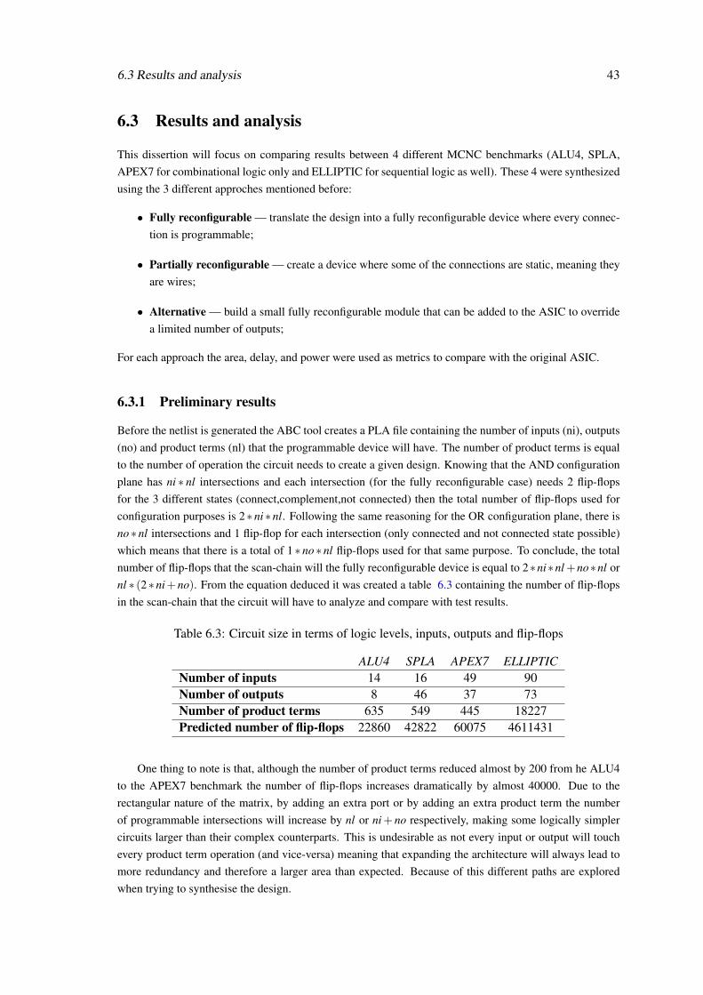
6.3 Results and analysis 43
6.3 Results and analysis
This dissertion will focus on comparing results between 4 different MCNC benchmarks (ALU4, SPLA,APEX7 for combinational logic only and ELLIPTIC for sequential logic as well). These 4 were synthesizedusing the 3 different approches mentioned before:
• Fully reconfigurable — translate the design into a fully reconfigurable device where every connec-tion is programmable;
• Partially reconfigurable — create a device where some of the connections are static, meaning theyare wires;
• Alternative — build a small fully reconfigurable module that can be added to the ASIC to overridea limited number of outputs;
For each approach the area, delay, and power were used as metrics to compare with the original ASIC.
6.3.1 Preliminary results
Before the netlist is generated the ABC tool creates a PLA file containing the number of inputs (ni), outputs(no) and product terms (nl) that the programmable device will have. The number of product terms is equalto the number of operation the circuit needs to create a given design. Knowing that the AND configurationplane has ni ∗ nl intersections and each intersection (for the fully reconfigurable case) needs 2 flip-flopsfor the 3 different states (connect,complement,not connected) then the total number of flip-flops used forconfiguration purposes is 2∗ni∗nl. Following the same reasoning for the OR configuration plane, there isno∗nl intersections and 1 flip-flop for each intersection (only connected and not connected state possible)which means that there is a total of 1∗no∗nl flip-flops used for that same purpose. To conclude, the totalnumber of flip-flops that the scan-chain will the fully reconfigurable device is equal to 2∗ni∗nl+no∗nl ornl ∗ (2∗ni+no). From the equation deduced it was created a table 6.3 containing the number of flip-flopsin the scan-chain that the circuit will have to analyze and compare with test results.
Table 6.3: Circuit size in terms of logic levels, inputs, outputs and flip-flops
ALU4 SPLA APEX7 ELLIPTICNumber of inputs 14 16 49 90Number of outputs 8 46 37 73Number of product terms 635 549 445 18227Predicted number of flip-flops 22860 42822 60075 4611431
One thing to note is that, although the number of product terms reduced almost by 200 from he ALU4to the APEX7 benchmark the number of flip-flops increases dramatically by almost 40000. Due to therectangular nature of the matrix, by adding an extra port or by adding an extra product term the numberof programmable intersections will increase by nl or ni+ no respectively, making some logically simplercircuits larger than their complex counterparts. This is undesirable as not every input or output will touchevery product term operation (and vice-versa) meaning that expanding the architecture will always lead tomore redundancy and therefore a larger area than expected. Because of this different paths are exploredwhen trying to synthesise the design.
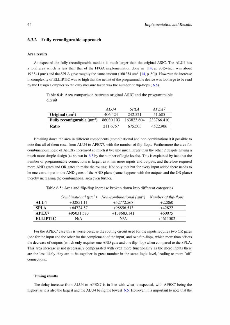
44 Implementation and Results
6.3.2 Fully reconfigurable approach
Area results
As expected the fully reconfigurable module is much larger than the original ASIC. The ALU4 hasa total area which is less than that of the FPGA implementation done in [14, p. 80](which was about192541 µm2) and the SPLA gave roughly the same amount (160254 µm2 [14, p. 80]). However the increasein complexity of ELLIPTIC was so high that the netlist of the programmable device was too large to be readby the Design Compiler so the only measure taken was the number of flip-flops ( 6.5).
Table 6.4: Area comparison between original ASIC and the programmablecircuit
ALU4 SPLA APEX7Original (µm2) 406.424 242.521 51.685Fully reconfigurable (µm2) 86030.103 163823.604 233766.410Ratio 211.6757 675.503 4522.906
Breaking down the area in different components (combinational and non-combinational) it possible tonote that all of them rose, from ALU4 to APEX7, with the number of flip-flops. Furthermore the area forcombinational logic of APEX7 increased so much it became much larger than the other 2 despite having amuch more simple design (as shown in 6.3 by the number of logic levels). This is explained by fact that thenumber of programmable connections is larger, as it has more inputs and outputs, and therefore requiredmore AND gates and OR gates to make the routing. Not only that but for every input added there needs tobe one extra input in the AND gates of the AND plane (same happens with the outputs and the OR plane)thereby increasing the combinational area even further.
Table 6.5: Area and flip-flop increase broken down into different categories
Combinational (µm2) Non-combinational (µm2) Number of flip-flopsALU4 +32851.11 +52772.568 +22860SPLA +64724.57 +98856.513 +42822APEX7 +95031.583 +138683.141 +60075ELLIPTIC N/A N/A +4611502
For the APEX7 case this is worse because the routing circuit used for the inputs requires two OR gates(one for the input and the other for the complement of the input) and two flip-flops, which more than offsetsthe decrease of outputs (which only requires one AND gate and one flip-flop) when compared to the SPLA.This area increase is not necessarily compensated with even more functionality as the more inputs thereare the less likely they are to be together in great number in the same logic level, leading to more ’off’connections.
Timing results
The delay increase from ALU4 to APEX7 is in line with what is expected, with APEX7 being thehighest as it is also the largest and the ALU4 being the lowest 6.6. However, it is important to note that the
6.3 Results and analysis 45
increase in delay is not as marked as the increase in area due to the fact that the routing circuit is the samefor every device independent of size with the major change happening in the AND plane or the OR plane.In this case the change in input/output number leads to different gate size to accomodate it, which in turnchanges the delay in that plane.
Table 6.6: Data arrival time comparison for each test cir-cuit
ALU4 SPLA APEX7Original (ns) 0.46 0.34 0.19Fully reconfigurable (ns) 1.84 2.30 2.86Ratio 4.00 6.76 250.53
As for the ratio between the original and the fully reconfigurable circuit, it is explained by the overheadadded to the routing plus the gate size increase in the AND/OR plane which increases delay significantly.
Power consumption
As expected, the power consumption of the electrical circuits increases in relation to its size. This isreflected by the extra internal power consuption from the added flip-flops as well as the leakage from thecircuitry added for routing.
Table 6.7: Power comparisom between original ASIC and the pro-grammable circuit
ALU4 SPLA APEX7Original (mW) 0.237 0.125 2.600e-2Fully reconfigurable (mW) 37.098 72.409 116.306Ratio 156.532 579.272 4473.308
Table 6.8: Power increase broken down into different categories
Internal (mW) Switching (mW) Leakage (mW)ALU4 +8.910 +7.4626 +20.409SPLA +19.692 +12.423 +40.169APEX7 +34.268 +24.493 +57.531
6.3.3 Partially reconfigurable approach
To create partial reconfigurability two main situations were considered: one were logic between register wasthe target of recofiguration and another where the all the logic was considered instead (see fig. 6.2). Verify-ing these two cases could prove that it is possible to differenciate the sequential part from the combinationalpart in the architecture which can allow for other, more local, optimizations.
46 Implementation and Results
(a) Case1 (sequential logic only) (b) Case2 (combinational logic only)
Figure 6.2: Cases for partial reconfiguration
Experiments
To verify if these two cases hold true, two experiments were built for a Synopsys design. One wouldconsist of a simple input wire swap before it goes into a register module and another consisting of the samebut with register output wires instead.
Table 6.9: Flip-flop count comparison
Experiment ResultSwap circuit input in register modules Input wires swapped position in the AND configuration
planes for that case specifically; Input state swappedrows in the PLA matrix;
Swap circuit outputs in register modules Resulting circuit is equivalent to doing the wire swapp;Overall shuffle of the entire PLA matrix, where input wiresmay swapp collumns or rows can change positions as well;
The case 2 was easy to prove and yielded satisfactory results. However changing the internal sequentiallogic (even if it is just wire placements) caused ABC to create completly different matrices, even though theresulting change to reconfigurable module is simple. Most of the changes that ABC makes for the secondexperiment are within reach of case 1 but the bitstream generation process needs to take into account thedifferent order at which it needs to make the bitstream (result of column swaps).
Flip-flop count
After the experiments were made, both cases of partial reconfigurability were aplied to the ELLIPTICbenchmark and the results of the flip-flop count were measured (the modules created for the ELLIPTICbenchmark could not be synthesized as was explained in 6.3.2) and compared to the fully-reconfigurableconterpart. The ratio for both cases went from about 25% to 75% for the designs tested at Synopsys as welland it depended on the wheight that the sequential logic had on overall design.
Table 6.10: Flip-flop count comparison
ELLIPTICFully reconfig 4611502Case1/fully reconfig ratio 0.842Case2/fully reconfig ratio 0.158
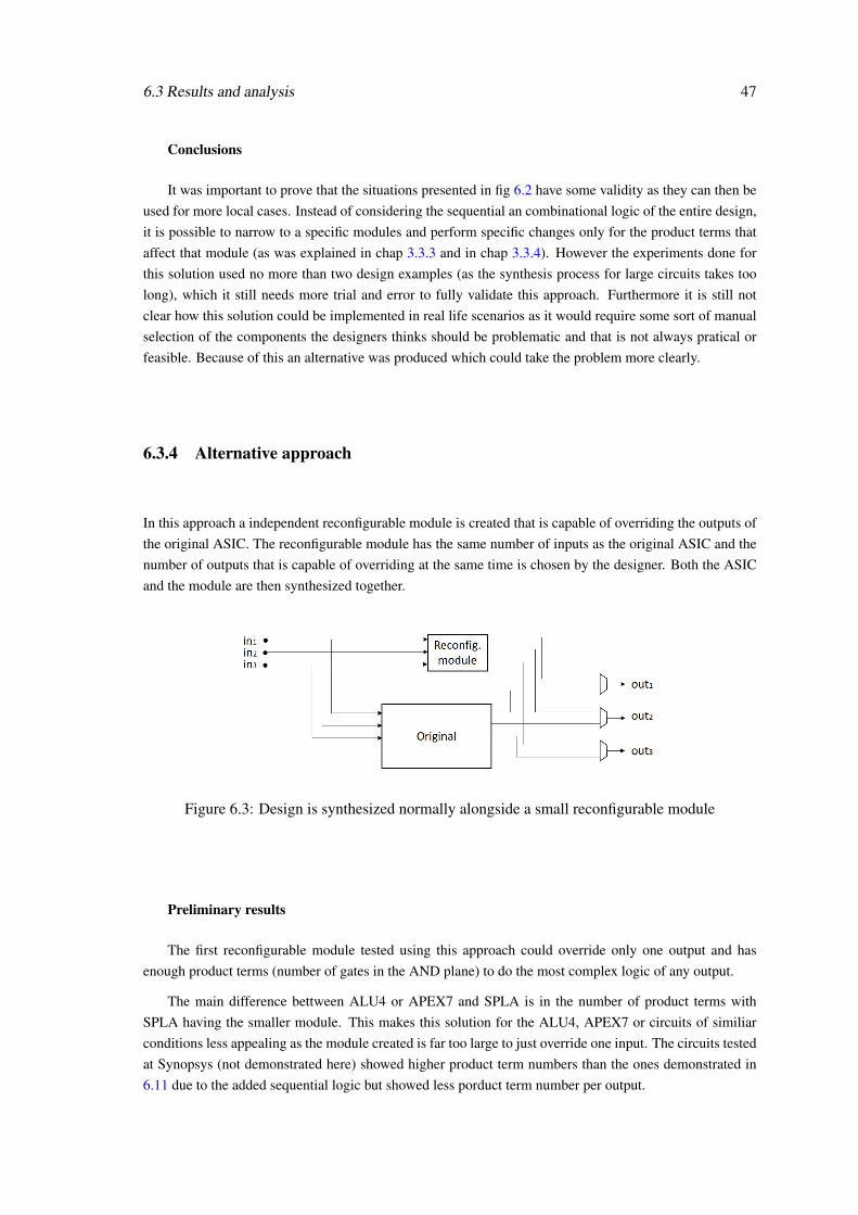
6.3 Results and analysis 47
Conclusions
It was important to prove that the situations presented in fig 6.2 have some validity as they can then beused for more local cases. Instead of considering the sequential an combinational logic of the entire design,it is possible to narrow to a specific modules and perform specific changes only for the product terms thataffect that module (as was explained in chap 3.3.3 and in chap 3.3.4). However the experiments done forthis solution used no more than two design examples (as the synthesis process for large circuits takes toolong), which it still needs more trial and error to fully validate this approach. Furthermore it is still notclear how this solution could be implemented in real life scenarios as it would require some sort of manualselection of the components the designers thinks should be problematic and that is not always pratical orfeasible. Because of this an alternative was produced which could take the problem more clearly.
6.3.4 Alternative approach
In this approach a independent reconfigurable module is created that is capable of overriding the outputs ofthe original ASIC. The reconfigurable module has the same number of inputs as the original ASIC and thenumber of outputs that is capable of overriding at the same time is chosen by the designer. Both the ASICand the module are then synthesized together.
Figure 6.3: Design is synthesized normally alongside a small reconfigurable module
Preliminary results
The first reconfigurable module tested using this approach could override only one output and hasenough product terms (number of gates in the AND plane) to do the most complex logic of any output.
The main difference bettween ALU4 or APEX7 and SPLA is in the number of product terms withSPLA having the smaller module. This makes this solution for the ALU4, APEX7 or circuits of similiarconditions less appealing as the module created is far too large to just override one input. The circuits testedat Synopsys (not demonstrated here) showed higher product term numbers than the ones demonstrated in6.11 due to the added sequential logic but showed less porduct term number per output.
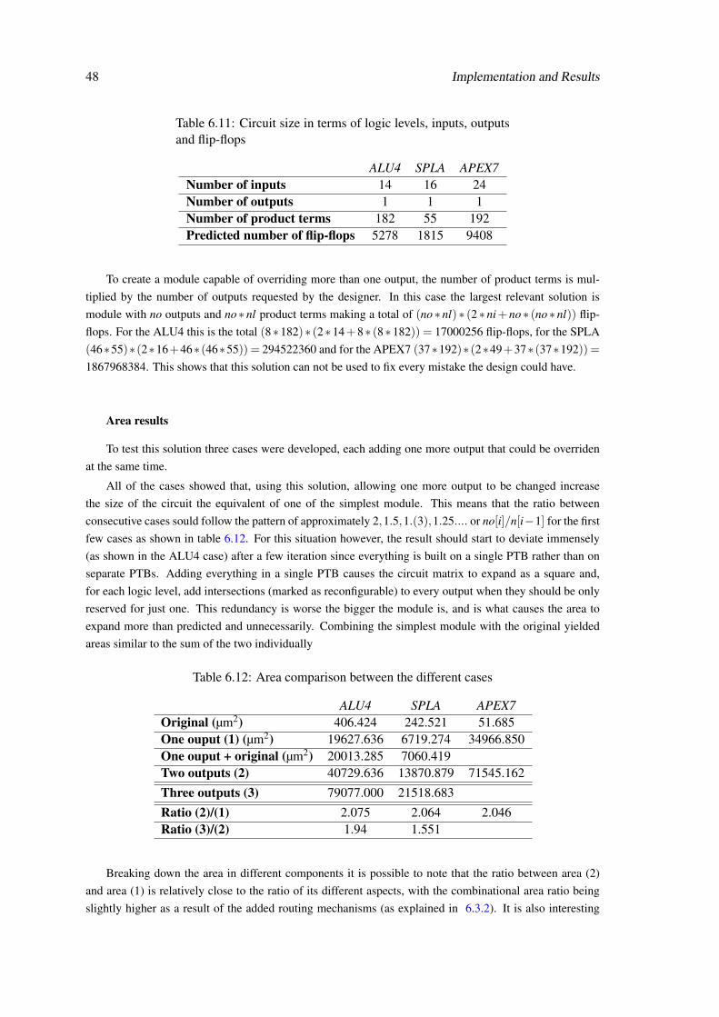
48 Implementation and Results
Table 6.11: Circuit size in terms of logic levels, inputs, outputsand flip-flops
ALU4 SPLA APEX7Number of inputs 14 16 24Number of outputs 1 1 1Number of product terms 182 55 192Predicted number of flip-flops 5278 1815 9408
To create a module capable of overriding more than one output, the number of product terms is mul-tiplied by the number of outputs requested by the designer. In this case the largest relevant solution ismodule with no outputs and no∗nl product terms making a total of (no∗nl)∗ (2∗ni+no∗ (no∗nl)) flip-flops. For the ALU4 this is the total (8∗182)∗ (2∗14+8∗ (8∗182)) = 17000256 flip-flops, for the SPLA(46∗55)∗(2∗16+46∗(46∗55)) = 294522360 and for the APEX7 (37∗192)∗(2∗49+37∗(37∗192)) =1867968384. This shows that this solution can not be used to fix every mistake the design could have.
Area results
To test this solution three cases were developed, each adding one more output that could be overridenat the same time.
All of the cases showed that, using this solution, allowing one more output to be changed increasethe size of the circuit the equivalent of one of the simplest module. This means that the ratio betweenconsecutive cases sould follow the pattern of approximately 2,1.5,1.(3),1.25.... or no[i]/n[i−1] for the firstfew cases as shown in table 6.12. For this situation however, the result should start to deviate immensely(as shown in the ALU4 case) after a few iteration since everything is built on a single PTB rather than onseparate PTBs. Adding everything in a single PTB causes the circuit matrix to expand as a square and,for each logic level, add intersections (marked as reconfigurable) to every output when they should be onlyreserved for just one. This redundancy is worse the bigger the module is, and is what causes the area toexpand more than predicted and unnecessarily. Combining the simplest module with the original yieldedareas similar to the sum of the two individually
Table 6.12: Area comparison between the different cases
ALU4 SPLA APEX7Original (µm2) 406.424 242.521 51.685One ouput (1) (µm2) 19627.636 6719.274 34966.850One ouput + original (µm2) 20013.285 7060.419Two outputs (2) 40729.636 13870.879 71545.162Three outputs (3) 79077.000 21518.683Ratio (2)/(1) 2.075 2.064 2.046Ratio (3)/(2) 1.94 1.551
Breaking down the area in different components it is possible to note that the ratio between area (2)and area (1) is relatively close to the ratio of its different aspects, with the combinational area ratio beingslightly higher as a result of the added routing mechanisms (as explained in 6.3.2). It is also interesting
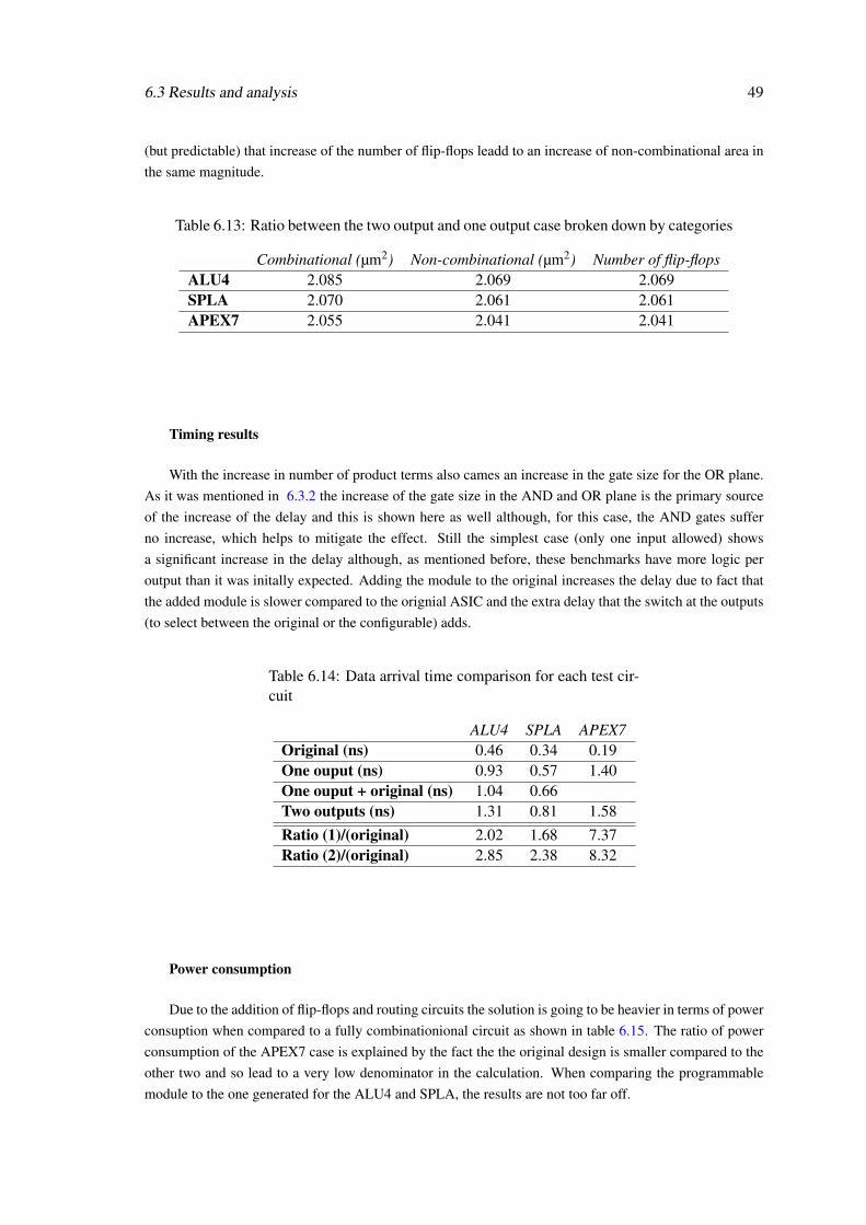
6.3 Results and analysis 49
(but predictable) that increase of the number of flip-flops leadd to an increase of non-combinational area inthe same magnitude.
Table 6.13: Ratio between the two output and one output case broken down by categories
Combinational (µm2) Non-combinational (µm2) Number of flip-flopsALU4 2.085 2.069 2.069SPLA 2.070 2.061 2.061APEX7 2.055 2.041 2.041
Timing results
With the increase in number of product terms also cames an increase in the gate size for the OR plane.As it was mentioned in 6.3.2 the increase of the gate size in the AND and OR plane is the primary sourceof the increase of the delay and this is shown here as well although, for this case, the AND gates sufferno increase, which helps to mitigate the effect. Still the simplest case (only one input allowed) showsa significant increase in the delay although, as mentioned before, these benchmarks have more logic peroutput than it was initally expected. Adding the module to the original increases the delay due to fact thatthe added module is slower compared to the orignial ASIC and the extra delay that the switch at the outputs(to select between the original or the configurable) adds.
Table 6.14: Data arrival time comparison for each test cir-cuit
ALU4 SPLA APEX7Original (ns) 0.46 0.34 0.19One ouput (ns) 0.93 0.57 1.40One ouput + original (ns) 1.04 0.66Two outputs (ns) 1.31 0.81 1.58Ratio (1)/(original) 2.02 1.68 7.37Ratio (2)/(original) 2.85 2.38 8.32
Power consumption
Due to the addition of flip-flops and routing circuits the solution is going to be heavier in terms of powerconsuption when compared to a fully combinationional circuit as shown in table 6.15. The ratio of powerconsumption of the APEX7 case is explained by the fact the the original design is smaller compared to theother two and so lead to a very low denominator in the calculation. When comparing the programmablemodule to the one generated for the ALU4 and SPLA, the results are not too far off.
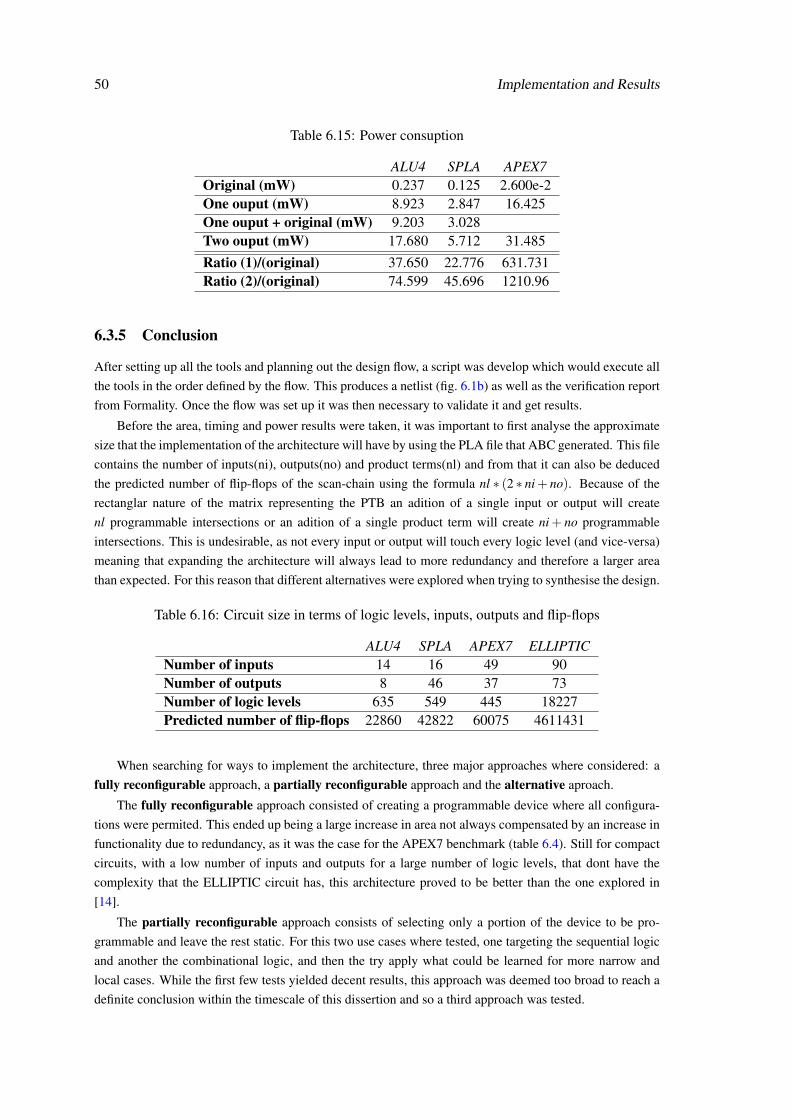
50 Implementation and Results
Table 6.15: Power consuption
ALU4 SPLA APEX7Original (mW) 0.237 0.125 2.600e-2One ouput (mW) 8.923 2.847 16.425One ouput + original (mW) 9.203 3.028Two ouput (mW) 17.680 5.712 31.485Ratio (1)/(original) 37.650 22.776 631.731Ratio (2)/(original) 74.599 45.696 1210.96
6.3.5 Conclusion
After setting up all the tools and planning out the design flow, a script was develop which would execute allthe tools in the order defined by the flow. This produces a netlist (fig. 6.1b) as well as the verification reportfrom Formality. Once the flow was set up it was then necessary to validate it and get results.
Before the area, timing and power results were taken, it was important to first analyse the approximatesize that the implementation of the architecture will have by using the PLA file that ABC generated. This filecontains the number of inputs(ni), outputs(no) and product terms(nl) and from that it can also be deducedthe predicted number of flip-flops of the scan-chain using the formula nl ∗ (2 ∗ ni+ no). Because of therectanglar nature of the matrix representing the PTB an adition of a single input or output will createnl programmable intersections or an adition of a single product term will create ni+ no programmableintersections. This is undesirable, as not every input or output will touch every logic level (and vice-versa)meaning that expanding the architecture will always lead to more redundancy and therefore a larger areathan expected. For this reason that different alternatives were explored when trying to synthesise the design.
Table 6.16: Circuit size in terms of logic levels, inputs, outputs and flip-flops
ALU4 SPLA APEX7 ELLIPTICNumber of inputs 14 16 49 90Number of outputs 8 46 37 73Number of logic levels 635 549 445 18227Predicted number of flip-flops 22860 42822 60075 4611431
When searching for ways to implement the architecture, three major approaches where considered: afully reconfigurable approach, a partially reconfigurable approach and the alternative aproach.
The fully reconfigurable approach consisted of creating a programmable device where all configura-tions were permited. This ended up being a large increase in area not always compensated by an increase infunctionality due to redundancy, as it was the case for the APEX7 benchmark (table 6.4). Still for compactcircuits, with a low number of inputs and outputs for a large number of logic levels, that dont have thecomplexity that the ELLIPTIC circuit has, this architecture proved to be better than the one explored in[14].
The partially reconfigurable approach consists of selecting only a portion of the device to be pro-grammable and leave the rest static. For this two use cases where tested, one targeting the sequential logicand another the combinational logic, and then the try apply what could be learned for more narrow andlocal cases. While the first few tests yielded decent results, this approach was deemed too broad to reach adefinite conclusion within the timescale of this dissertion and so a third approach was tested.

6.3 Results and analysis 51
The alternative and final approach involved a more simple case where a module would be created ca-pable of overriding one of more outputs (depending on necessity), which could be latter added to an ASIC.These modules had large (though more acceptable) area, but in part due to the fact that the benchmarksthat were tested on also had a lot of logic per output. However, even for sequential circuits that had moreacceptable number of product terms (like the ones tested at Synopsys), the modules ended up being of thesame size or bigger due to the added sequential logic. Despite this the solution shows more promise, as it ismore viable than the other two and more clear in its implementation with the cost-benefit better understood.That being said, in this solution the architecture used was not optimized (by removing unecessary configu-rations) nor was it tested in architectures that have less redundant configurations than the PTB, which couldhave made the results better.

52 Implementation and Results
Chapter 7
Conclusions and Future work
In this dissertion had the goal of creating a design flow where a programmable architecture that could beimplemented in a ASIC design while allowing optimizations to be done to that architecture so that it couldtarget more specific cases.
For that, chapter 2 started by introducing both the standard ASIC flow and programmable architecturesuch as FPGAs. The ASIC flow provided a basis by which the design flow could be developed upon whilethe study of programmable devices served the purpose of understanding which architecture would be mostsuited for the problem. The island style FPGA with LUT had already been developed before in [14] andit lead to area results which were unsuited for real-life cases so another more simple architecture followingthe PLA structure was adopted instead.
Once the base of the programmable architecture was decided chapter 3 focused on developing it. Inthis chapter the most important aspects decided were the routing used for the AND and OR inputs and theuse cases where the architecture could be changed to achieve a more narrow purpose and therefore consumeless area.
The chapters 4 and 5 described the design flow and the support tools used to implement it respectively.The design flow follows the standard synthesis followed by the physical implementation with the addedbitstream generation step before verification. It was constructed with the intent of the core components(the ones built for this thesis) being easily replaceable with those of a normal ASIC design and vice-versa.Furthermore it was also to facilitate introduction of different approaches to the architecture implementation.
Finaly chapters 6 explains leftover details of the implementation, such as the script used to executeall the tools, design issues or how the netlist was produced, and exposes the results of the experimentsmade. When searching for ways to implement the architecture 3 major approaches where considered: afully reconfigurable approach, a partially reconfigurable approach and the alternative aproach. Thefully reconfigurable device generated using the PTB architecture showed areas below or closer to the onesfrom "Automatic implementation of a re-configurable logic over ASIC design flow" [14] but for circuitswith more with more complex logic it gave far worse results comparatively. Either way ratios that surpass200 are unthinkable for real world circuits and so of all the 3 approaches the third was more viable as it hada more reasonable area while the second one was difficult to implement.
Still there aspects not corrected in the architecture and the design flow and experiments not made dueto time constrains such as:
53
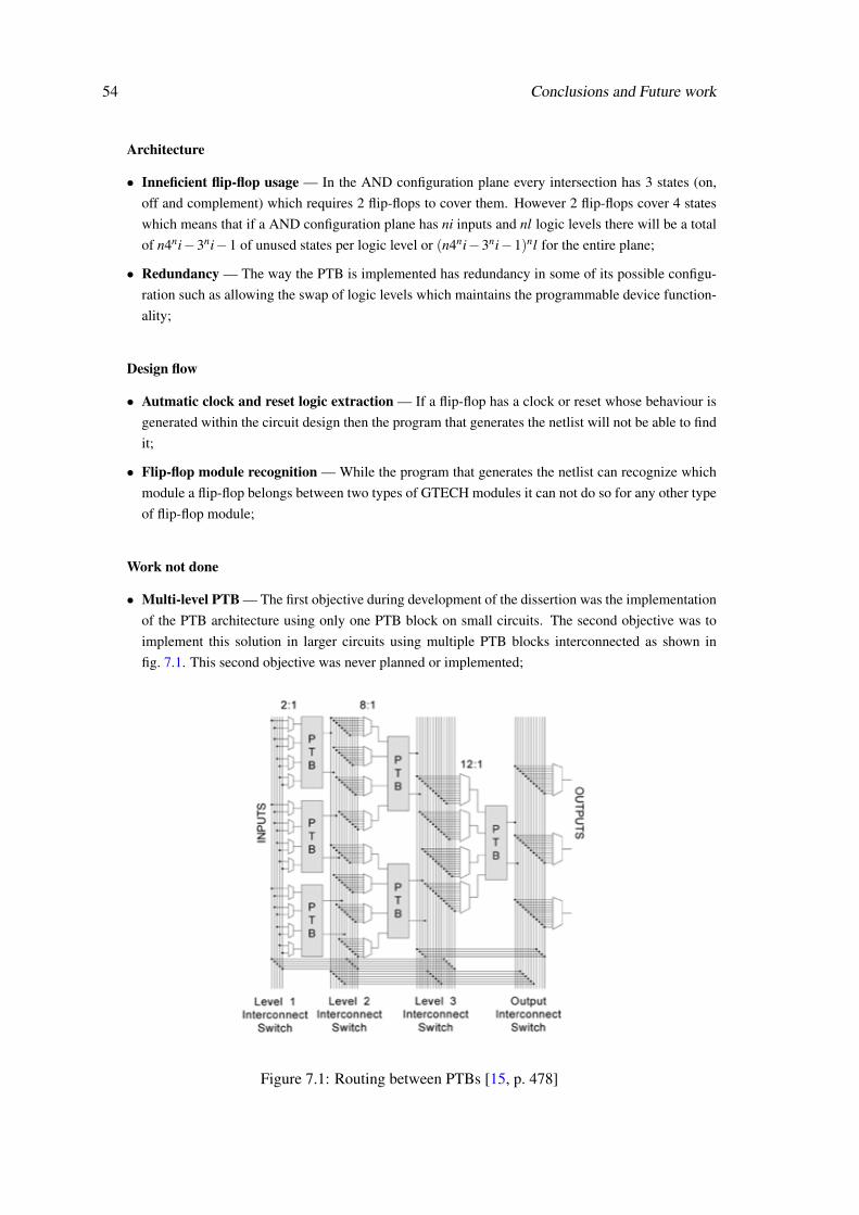
54 Conclusions and Future work
Architecture
• Inneficient flip-flop usage — In the AND configuration plane every intersection has 3 states (on,off and complement) which requires 2 flip-flops to cover them. However 2 flip-flops cover 4 stateswhich means that if a AND configuration plane has ni inputs and nl logic levels there will be a totalof n4ni−3ni−1 of unused states per logic level or (n4ni−3ni−1)nl for the entire plane;
• Redundancy — The way the PTB is implemented has redundancy in some of its possible configu-ration such as allowing the swap of logic levels which maintains the programmable device function-ality;
Design flow
• Autmatic clock and reset logic extraction — If a flip-flop has a clock or reset whose behaviour isgenerated within the circuit design then the program that generates the netlist will not be able to findit;
• Flip-flop module recognition — While the program that generates the netlist can recognize whichmodule a flip-flop belongs between two types of GTECH modules it can not do so for any other typeof flip-flop module;
Work not done
• Multi-level PTB — The first objective during development of the dissertion was the implementationof the PTB architecture using only one PTB block on small circuits. The second objective was toimplement this solution in larger circuits using multiple PTB blocks interconnected as shown infig. 7.1. This second objective was never planned or implemented;
Figure 7.1: Routing between PTBs [15, p. 478]
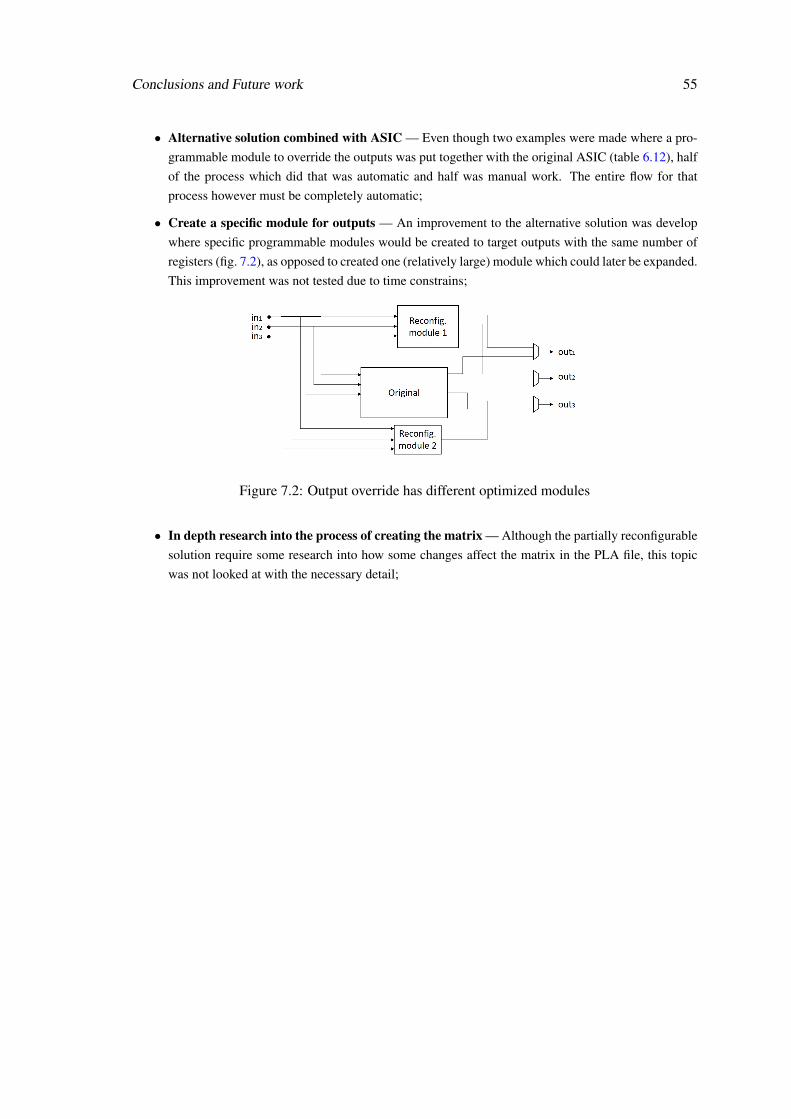
Conclusions and Future work 55
• Alternative solution combined with ASIC — Even though two examples were made where a pro-grammable module to override the outputs was put together with the original ASIC (table 6.12), halfof the process which did that was automatic and half was manual work. The entire flow for thatprocess however must be completely automatic;
• Create a specific module for outputs — An improvement to the alternative solution was developwhere specific programmable modules would be created to target outputs with the same number ofregisters (fig. 7.2), as opposed to created one (relatively large) module which could later be expanded.This improvement was not tested due to time constrains;
Figure 7.2: Output override has different optimized modules
• In depth research into the process of creating the matrix — Although the partially reconfigurablesolution require some research into how some changes affect the matrix in the PLA file, this topicwas not looked at with the necessary detail;

56 Conclusions and Future work
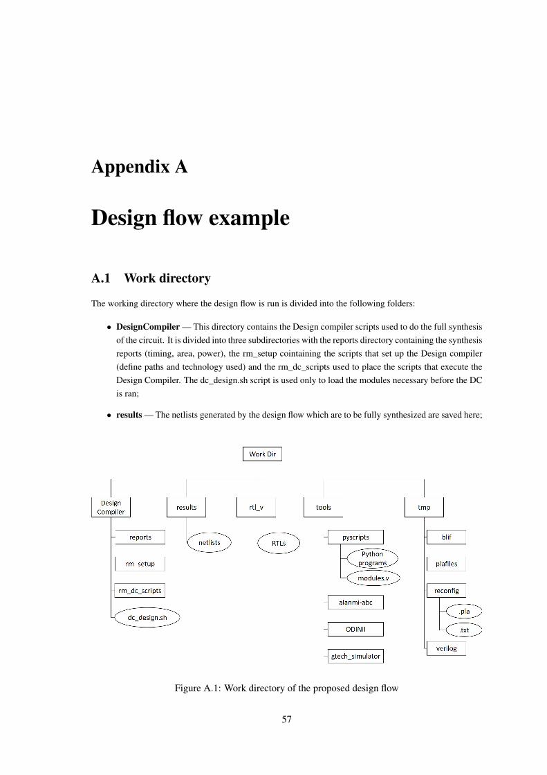
Appendix A
Design flow example
A.1 Work directory
The working directory where the design flow is run is divided into the following folders:
• DesignCompiler — This directory contains the Design compiler scripts used to do the full synthesisof the circuit. It is divided into three subdirectories with the reports directory containing the synthesisreports (timing, area, power), the rm_setup cointaining the scripts that set up the Design compiler(define paths and technology used) and the rm_dc_scripts used to place the scripts that execute theDesign Compiler. The dc_design.sh script is used only to load the modules necessary before the DCis ran;
• results — The netlists generated by the design flow which are to be fully synthesized are saved here;
Figure A.1: Work directory of the proposed design flow
57
58 Design flow example
• rtl_v — The RTLs to be processed by the design flow are placed in this folder;
• tools — Every tool used has its own folder placed in this directory. A directory similiar to theDesignCompiler was placed here but modified to generate a GTECH netlist instead of doing a fullsynthesis pocedure;
• tmp — For every file generated by the design flow (pla, blif and verilog files) has its own folder here.The circuit description (in txt format) and the reconfigurable PLA (in pla format) generated by theflow are placed in the reconfig directory;
A.2 Running the design flow script
The script used to run the flow takes in as arguments the RTL directory and name separately and producesthe netlist as well suplementary files for the reconfiguration phase. To run the main flow the syntax is asfollows:
. / d e s i g n f l o w . sh < d i r e c t o r y > <RTL name>
In case the designer wants verify if a modification made is compatible with the circuit previouslygenerated it needs to change the name of the new RTL to <original RTL name>_modified.v and run thescript configflow.sh in the same way as the designflow.sh
A.3 Programmable matrix generation
At some point in the flow a PLA matrix is generated which is then used to create the programmable device.However before the netlist of the device is built the matrix must undergo a process that translate from a staticto a reconfigurable representation. As was explained in chapter 4 this consists of replacing the elementsof the matrix with an ’x’ in the intersections that were deemed useful to be reconfigured, or ,in specialcases, resizing the matrix to fit more narrow purposes. The decisions that determine where that happensare dependent on the approach taken (fully reconfigurable, partially reconfigurable or alternative). The nextsubsections are dedicated to explaining the coding behind these appraoches.
A.3.1 Fully reconfigurable
In case the circuit is to be fully reconfigurable the matrix representing it is replaced by one where eachelement is open to all three states (1,0 and ’-’) or, in other words, has the state ’x’. This is done bycreating a method that receives any given plane (AND configuration plane or OR configuration plane) anda genericVector (whose values are either ’x’ or ’-’) that replaces each row, changing the values of the rowelements to ’x’ except the ones not covered by the vector. To create a fully reconfigurable matrix the vectorgiven needs to only have the ’x’ state in each of its elements.
def g e n e r a t e C o n f i g u r a t i o n M a t r i x ( p lane , g e n e r i c V e c t o r ) :c o n f i g u r a t i o n M a t r i x = [ ]f o r l i n e in p l a n e :
l i n e = l i s t ( l i n e )f o r n , e l e m e n t in enumerate ( g e n e r i c V e c t o r ) :
i f e l e m e n t == ’ x ’ :
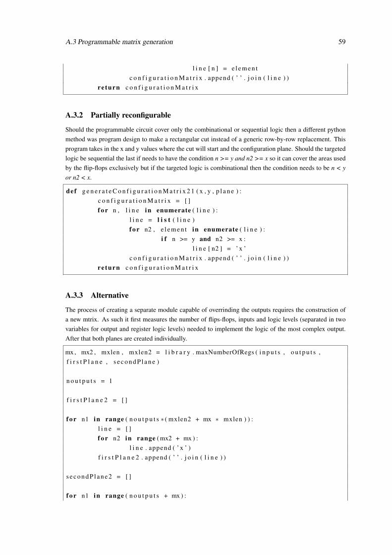
A.3 Programmable matrix generation 59
l i n e [ n ] = e l e m e n tc o n f i g u r a t i o n M a t r i x . append ( ’ ’ . j o i n ( l i n e ) )
re turn c o n f i g u r a t i o n M a t r i x
A.3.2 Partially reconfigurable
Should the programmable circuit cover only the combinational or sequential logic then a different pythonmethod was program design to make a rectangular cut instead of a generic row-by-row replacement. Thisprogram takes in the x and y values where the cut will start and the configuration plane. Should the targetedlogic be sequential the last if needs to have the condition n >= y and n2 >= x so it can cover the areas usedby the flip-flops exclusively but if the targeted logic is combinational then the condition needs to be n < yor n2 < x.
def g e n e r a t e C o n f i g u r a t i o n M a t r i x 2 1 ( x , y , p l a n e ) :c o n f i g u r a t i o n M a t r i x = [ ]f o r n , l i n e in enumerate ( l i n e ) :
l i n e = l i s t ( l i n e )f o r n2 , e l e m e n t in enumerate ( l i n e ) :
i f n >= y and n2 >= x :l i n e [ n2 ] = ’ x ’
c o n f i g u r a t i o n M a t r i x . append ( ’ ’ . j o i n ( l i n e ) )re turn c o n f i g u r a t i o n M a t r i x
A.3.3 Alternative
The process of creating a separate module capable of overrinding the outputs requires the construction ofa new mtrix. As such it first measures the number of flips-flops, inputs and logic levels (separated in twovariables for output and register logic levels) needed to implement the logic of the most complex output.After that both planes are created individually.
mx , mx2 , mxlen , mxlen2 = l i b r a r y . maxNumberOfRegs ( i n p u t s , o u t p u t s ,f i r s t P l a n e , s e c o n d P l a n e )
n o u t p u t s = 1
f i r s t P l a n e 2 = [ ]
f o r n1 in range ( n o u t p u t s ∗ ( mxlen2 + mx ∗ mxlen ) ) :l i n e = [ ]f o r n2 in range ( mx2 + mx ) :
l i n e . append ( ’ x ’ )f i r s t P l a n e 2 . append ( ’ ’ . j o i n ( l i n e ) )
s e c o n d P l a n e 2 = [ ]
f o r n1 in range ( n o u t p u t s + mx ) :
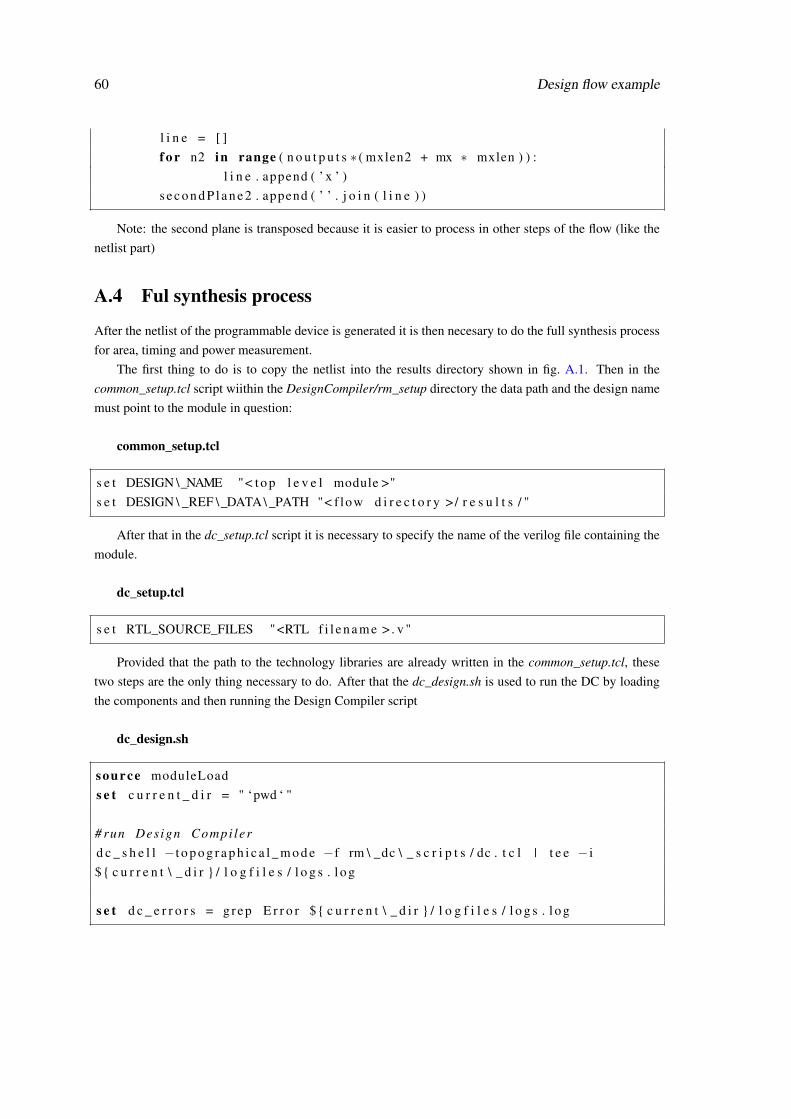
60 Design flow example
l i n e = [ ]f o r n2 in range ( n o u t p u t s ∗ ( mxlen2 + mx ∗ mxlen ) ) :
l i n e . append ( ’ x ’ )s e c o n d P l a n e 2 . append ( ’ ’ . j o i n ( l i n e ) )
Note: the second plane is transposed because it is easier to process in other steps of the flow (like thenetlist part)
A.4 Ful synthesis process
After the netlist of the programmable device is generated it is then necesary to do the full synthesis processfor area, timing and power measurement.
The first thing to do is to copy the netlist into the results directory shown in fig. A.1. Then in thecommon_setup.tcl script wiithin the DesignCompiler/rm_setup directory the data path and the design namemust point to the module in question:
common_setup.tcl
s e t DESIGN \_NAME "< t o p l e v e l module >"s e t DESIGN \ _REF \_DATA\ _PATH "< f low d i r e c t o r y > / r e s u l t s / "
After that in the dc_setup.tcl script it is necessary to specify the name of the verilog file containing themodule.
dc_setup.tcl
s e t RTL_SOURCE_FILES "<RTL f i l e n a m e > . v "
Provided that the path to the technology libraries are already written in the common_setup.tcl, thesetwo steps are the only thing necessary to do. After that the dc_design.sh is used to run the DC by loadingthe components and then running the Design Compiler script
dc_design.sh
source moduleLoads e t c u r r e n t _ d i r = " ‘pwd ‘ "
# run Design Compi lerd c _ s h e l l −t o p o g r a p h i c a l _ m o d e −f rm \ _dc \ _ s c r i p t s / dc . t c l | t e e − i${ c u r r e n t \ _ d i r } / l o g f i l e s / l o g s . l o g
s e t d c _ e r r o r s = g rep E r r o r ${ c u r r e n t \ _ d i r } / l o g f i l e s / l o g s . l o g
References
[1] Ise design suite tool. https://www.xilinx.com/support/documentation/sw_manuals/xilinx14_7/irn.pdf. Accessed: 2018-01-30.
[2] Spartan-6 fpga. https://www.xilinx.com/support/documentation/data_sheets/ds160.pdf. Accessed: 2018-01-30.
[3] Verilog to routing. https://docs.verilogtorouting.org/en/latest/, November 1997.Open source tools for FPGA architecture and CAD research.
[4] Robert Brayton Alan Mishchenko, Satrajit Chatterjee. DAG-Aware AIG Rewriting: a fresh look atcombinational logic synthesis. In Design Automation Conference, July 2006.
[5] Vaughn Betz, Jonathan Rose, and Alexander Marquardt. Architecture and cad for deepsubmicronfpgas. December 2012.
[6] MVSIS Group. MVSIS: Logic Synthesis and Verification. https://ptolemy.berkeley.edu/projects/embedded/mvsis/.
[7] Abbas El Gamal Jonathan Rose and Alberto Sangiovanni-Vicentelli. Architecture of field-programmable gate arrays. In Proceedings of the IEEE, pages 1013–1029, 1993.
[8] Chong Ming Lin. Pla design in nand structure. IEEE Transactions on Very Large Scale Integration(VLSI) Systems, pages 474–488, may 2006.
[9] Jason Luu, Jeff Goeders, Michael Wainberg, Andrew Somerville, Thien Yu, Konstantin Nasartschuk,Miad Nasr, Sen Wang, Tim Liu, Norrudin Ahmed, Kenneth B. Kent, Jason Anderson, Jonathan Rose,and Vaughn Betz. VTR 7.0: Next Generation Architecture and CAD System for FPGAs. ACM Trans.Reconfigurable Technol. Syst, pages 7(2):6:1–6:30, June 2004.
[10] University of California. Berkeley Logic Interchange Format (BLIF). https://www.cse.iitb.ac.in/~supratik/courses/cs226/spr16/blif.pdf, 07 1992.
[11] Ellen M. Sentovich, Kanwar Jit Singh, Luciano Lavagno, Cho Moon, Rajeev Murgai, Alexander Sal-danha, Hamid Savoj, Paul R. Stephan, Robert K. Brayton, and Albeno Sangiovanni-Vincentelli. SIS:A System for Sequential Circuit Synthesis. Technical report, Department of Electrical Engineeringand Computer Science, University of California, 05 1992.
[12] Michael John Sebastian Smith. Application-specific integrated circuits. Addison-Wesley Professionaland 1 edition, 1997.
[13] Berkeley Logic Synthesis and Verification Group. ABC: A System for Sequential Synthesis andVerification. http://people.eecs.berkeley.edu/~alanmi/abc/, 03 2018.
[14] José Delfim Ribeiro Valverde. Automatic implementation of a re-configurable logic over ASIC designflow, July 2017. master’s thesis, Faculdade de Engenharia e Universidade do Porto.
[15] Andy Yan and Steven J. E. Wilton. Product-term-based synthesizable embedded programmable logiccores. IEEE Transactions on Very Large Scale Integration (VLSI) Systems, pages 474–488, may 2006.
[16] Saeyang Yang. Logic synthesis and optimization benchmarks user guide version 3.0. MicroelectronicsCenter of North Carolina (MCNC), 1991.
61


![An Area Optimized Implementation of AES S-Box Based on ... · multiplication is optimized by CSE algorithm. The implementation of S-Box proposed in [7] has the smallest area [4]](https://img.pdfslide.us/doc/110x75/5ede6350ad6a402d6669b5bf/an-area-optimized-implementation-of-aes-s-box-based-on-multiplication-is-optimized.jpg)