Embed Size (px)
Citation preview
AC 2010-1449: STUDENT-CREATED LABORATORY EXERCISES FOR ADIGITAL SYSTEMS DESIGN COURSE USING HDL AND PLDS
Daniel McCarthy, University of WyomingDaniel D. McCarthy, M.S.E.E., was a graduate student in the Department of Electrical andComputer Engineering at the University of Wyoming, Laramie, WY, from which he receivedboth the BS in Computer Engineering and the MSEE degrees. He is a member of Tau Beta Pi andMortar Board.
Cameron Wright, University of WyomingCameron H. G. Wright, Ph.D, P.E., is an Associate Professor in the Department of Electrical andComputer Engineering at the University of Wyoming, Laramie, WY. He was formerly Professorand Deputy Department Head of the Electrical Engineerng Deparment at the U.S. Air ForceAcademy. His research interests include signal and image processing, real-time embeddedcomputer systems, biomedical instrumentation, and engineering education, and is the author orco-author of over 180 publications including papers, books, and book chapters. He is a member ofASEE, IEEE, SPIE, NSPE, BMES, Tau Beta Pi, and Eta Kappa Nu; he is an active ABETevaluator and NCEES exam committee member. E-mail: [email protected]
Steven Barrett, University of WyomingSteven F. Barrett, Ph.D., P.E. received the BS Electronic Engineering Technology from theUniversity of Nebraska at Omaha in 1979, the M.E.E.E. from the University of Idaho at Moscowin 1986, and the Ph.D. from The University of Texas at Austin in 1993. He was formally anactive duty faculty member at the United States Air Force Academy, Colorado and is now anAssociate Professor of Electrical and Computer Engineering, University of Wyoming. He is amember of IEEE (senior) and Tau Beta Pi (chief faculty advisor). His research interests includedigital and analog image processing, computer-assisted laser surgery, and embedded controllersystems. He is a registered Professional Engineer in Wyoming and Colorado. He co-wrote withDr. Daniel Pack five textbooks on microcontrollers and embedded systems. In 2004, Barrett wasnamed “Wyoming Professor of the Year” by the Carnegie Foundation for the Advancement ofTeaching and in 2008 was the recipient of the National Society of Professional Engineers (NSPE)Professional Engineers in Higher Education, Engineering Education Excellence Award.
Jerry Hamann, University of WyomingJerry C. Hamann received the B.S. in Electrical Engineering with a Bioengineering Option fromthe University of Wyoming in 1984. He then worked for the Loveland Instrument Division ofHewlett-Packard before returning to the University of Wyoming to complete the M.S. inElectrical Engineering in 1988. Sharing time as a lecturer and National Science FoundationGraduate Fellow, he completed the Ph.D. in Electrical Engineering at the University of Wisconsinin 1993. As a faculty member at the University of Wyoming since 1993, Jerry has pursuedresearch interests in applied robotics and control, signal processing, and higher education teachingand learning. He directed the University of Wyoming Hewlett Foundation Engineering Schools ofthe West Initiative until 2008, which is focused upon enhancing the recruitment, retention andquality of undergraduate engineering students. He now serves as Head, Department of ComputerScience.
© American Society for Engineering Education, 2010
Page 15.1115.1
Student-Created Laboratory Exercises for the Digital
Systems Design Course Using HDL and PLDs
Abstract
The concepts presented in an introductory digital systems design lecture are often difficult
for students to comprehend fully. In order to aid in this understanding, laboratory exercises
are often assigned in order to reinforce the concepts introduced in lecture. These lab exercises
also expose students to hardware, software, and hardware description languages used by indus-
try professionals. We have been experimenting with a new paradigm for lab exercise creation,
whereby previous students of a course are recruited to create new lab exercises for the course, a
method we call “By Students, For Students” that we have tested with several different courses.
This paper describes the result of applying this paradigm to a four semester hour introductory
digital systems design course typically taken by sophomore electrical engineering and com-
puter engineering majors. The lab exercises involve considerable use of programmable logic
and the Verilog hardware description language (HDL). Interestingly, the student-created lab
exercises tended to be more challenging than the previous set of faculty-created lab exercises.
1 Introduction
The concepts presented in a digital systems design lecture may be difficult for some undergraduate
students to fully grasp. In order to aid in students’ understanding, laboratory exercises are often
used in conjunction with traditional lectures to present tough concepts in an electrical engineering
courses like digital systems design.1–5
We have been experimenting with a new paradigm for lab exercise creation, whereby previous
students of a course are recruited to create new lab exercises for the course, a method we call “By
Students, For Students” that we have tested with several different courses. This paper describes
the lab exercises that resulted from applying this paradigm to a four semester hour introductory
digital systems design course (EE2390) typically taken by sophomore electrical engineering and
computer engineering majors. The course includes hands-on use of Xilinx’s professional-grade
electronic design automation (EDA) software, Xilinx CPLDs, Atmel PLDs, and even one lab exer-
cise using discrete logic chips. Most lab exercises involve considerable use of the Verilog hardware
description language (HDL). Interestingly, the student-created lab exercises for EE2390 tended to
be more challenging than the previous set of faculty-created lab exercises. Feedback from gradu-
ate student Teaching Assistants (TAs) who taught both versions of the lab exercises confirms the
efficacy of the student-created content.
Page 15.1115.2
EE2390 is a four credit hour course offered during the Spring and Fall semesters at the University
of Wyoming. It has a prerequisite of Calculus II and is designed to be taken during a student’s
sophomore year. The course is taught using the fourth edition of Digital Design by M. M. Mano
and M. D. Ciletti.6 The core topics covered in this course are:
• binary logic,
• digital logic gates,
• reduction of Boolean expressions,
• combinational logic design,
• SSI, MSI, LSI combinational logic ICs,
• flip-flops,
• synchronous and asynchronous sequential systems,
• MSI and LSI sequential system ICs, and
• algorithmic state machines.
The lab exercises for EE2390 are used to supplement the various concepts covered in lecture.
Throughout the semester, many of the core topics covered in lecture are also covered in lab to
improve the students’ comprehension. However, improved understanding of lecture concepts is
not the only purpose for the lab exercises in EE2390. These lab exercises also expose students to
hardware, software and hardware description languages used by industry professionals.6–8 Some
of these include:
• Verilog hardware description language,
• Xilinx electronic design automation (EDA) software,
• Xilinx 95108 CPLD,
• CUPL hardware description language,
• Atmel WinCUPL software, and
• Atmel ATF22V10 PLD.
The primary reason for creating a new set of lab exercises for EE2390 was to “push” the students
to a higher level of understanding. The previous version of the lab exercises was created when
a previous edition of the text book was used; in that edition the coverage of Verilog was not
as extensive nor were there as many examples as in the latest edition. With the new textbook
edition and a more thorough coverage of using HDL with programmable logic in class came the
opportunity to challenge the students a bit more. However, a student’s perspective about how much
is too much of a challenge can be invaluable. This is part of the benefit of the “By Students, For
Students” method. Previous students of some course, who are usually by now graduate students,
are recruited to create new lab exercises for that course using their student perspective as a form
of insight that many professors have long forgotten. We have successfully used this approach with
several undergraduate courses.
Page 15.1115.3
2 Laboratory Setup
Each lab section for EE2390 takes place in the digital lab at the University of Wyoming. Students
attend one two hour lab section per week for 13 weeks out of the semester. When completing lab
exercises, students work in groups of two. Although the students are working collaboratively to
finish the in-lab portion of the lab exercises, each student is responsible for his/her own work and
their own lab notebook.
2.1 Laboratory Equipment
The digital lab at the University of Wyoming is equipped with all the necessary lab equipment,
hardware, and software for students to complete the assigned lab exercises. This includes:
• PCs running the Windows operating system,
• Elenco Model XK-550 (prototype board) Trainers,
• logic analyzers,
• oscilloscopes,
• multimeters,
• external power supplies,
• Xilinx’s 95108 CPLDs on custom PCBs,
• Atmel’s ATF22V10CQZ PLDs in DIP packaging,
• individual logic gate in DIP packaging,
• seven segment LEDs,
• ten segment bar graph LEDs,
• Xilinx ISE 10.1 software,
• ModelSim XE III/Starter 6.3c software, and
• Atmel WinCupl software.
2.2 Laboratory Manual
At the start of the semester each student is required to purchase a lab manual for EE2390.9 This
lab manual consists of:
• laboratory notebook procedures,
• pre-lab instructions for each lab,
• in-lab instructions for each lab,
• instructions on how to use all required software,
Page 15.1115.4
• information on the custom PCBs that interface with the Xilinx 95108 CPLDs,
• a datasheet for the Atmel ATF22V10CQZ PLD, and
• datasheets for all individual logic gate chips.
2.3 Laboratory Quizes
At the beginning of every lab section, students are given a quiz over the material covered in the
previous week’s lab. These quizzes are only a few questions in length and designed to be completed
in ten minutes or less.
2.4 Students’ Laboratory Notebook
At the beginning of the semester, each student is required to purchase a blank lab notebook. The
purpose of these notebooks is to get the students into the habit of keeping a valid lab notebook
whenever they are doing applicable engineering work. The requirements for these notebooks are
set forth in the beginning of the lab manual along with some generic guidelines as to what the
students should be including in their notebook. The first couple of labs also instruct the students
on exactly what should be placed into their lab notebooks. However, during the later labs, the
student is responsible for including the proper information in the lab notebook. At the beginning
of each lab, students submit these notebooks to the lab TA for grading. The TA grades the previous
week’s lab as well as the pre-lab exercises for the current week. In addition to the weekly grading
of the notebooks, a final grade is given to each student’s notebook at the end of semester by the
course professor.
3 Description of New Lab Exercises
3.1 Lab 1: Binary Arithmetic
3.1.1 Key Concepts
The key concepts addressed in this lab are:
• converting between the binary, hexadecimal, and decimal number systems;
• addition and subtraction of unsigned and signed 2’s complement numbers along with over-
flow detection;
• an introduction to the Xilinx and ModelSim software packages; and
• the simulation of a design using Xilinx and ModelSim software.
3.1.2 Pre-Lab Exercises
This pre-lab requires students to complete the addition and subtraction exercises shown in Table 1.
Students must use the binary number system in order to complete the operations and then convert
Page 15.1115.5
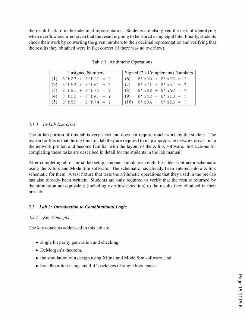
the result back to its hexadecimal representation. Students are also given the task of identifying
when overflow occurred given that the result is going to be stored using eight bits. Finally, students
check their work by converting the given numbers to their decimal representation and verifying that
the results they obtained were in fact correct (if there was no overflow).
Table 1: Arithmetic Operations
Unsigned Numbers Signed (2’s Complement) Numbers
(1) 8’h23 + 8’hCF = ? (6) 8’hDD + 8’hEE = ?
(2) 8’hA2 + 8’h61 = ? (7) 8’h71 + 8’h54 = ?
(3) 8’h81 + 8’h7D = ? (8) 8’h9E + 8’hAC = ?
(4) 8’hC0 - 8’hAF = ? (9) 8’h4E - 8’h1B = ?
(5) 8’h59 - 8’h74 = ? (10) 8’h8A - 8’h5B = ?
3.1.3 In-Lab Exercises
The in-lab portion of this lab is very short and does not require much work by the student. The
reason for this is that during this first lab they are required to map appropriate network drives, map
the network printer, and become familiar with the layout of the Xilinx software. Instructions for
completing these tasks are described in detail for the students in the lab manual.
After completing all of initial lab setup, students simulate an eight bit adder subtractor schematic
using the Xilinx and ModelSim software. The schematic has already been entered into a Xilinx
schematic for them. A test fixture that tests the arithmetic operations that they used in the pre-lab
has also already been written. Students are only required to verify that the results returned by
the simulation are equivalent (including overflow detection) to the results they obtained in their
pre-lab.
3.2 Lab 2: Introduction to Combinational Logic
3.2.1 Key Concepts
The key concepts addressed in this lab are:
• single bit parity generation and checking,
• DeMorgan’s theorem,
• the simulation of a design using Xilinx and ModelSim software, and
• breadboarding using small IC packages of single logic gates.
Page 15.1115.6
3.2.2 Pre-Lab Exercises
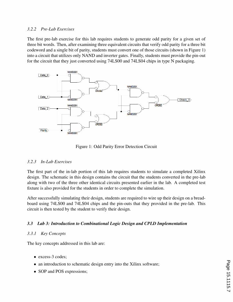
The first pre-lab exercise for this lab requires students to generate odd parity for a given set of
three bit words. Then, after examining three equivalent circuits that verify odd parity for a three bit
codeword and a single bit of parity, students must convert one of those circuits (shown in Figure 1)
into a circuit that utilizes only NAND and inverter gates. Finally, students must provide the pin-out
for the circuit that they just converted using 74LS00 and 74LS04 chips in type N packaging.
Figure 1: Odd Parity Error Detection Circuit
3.2.3 In-Lab Exercises
The first part of the in-lab portion of this lab requires students to simulate a completed Xilinx
design. The schematic in this design contains the circuit that the students converted in the pre-lab
along with two of the three other identical circuits presented earlier in the lab. A completed test
fixture is also provided for the students in order to complete the simulation.
After successfully simulating their design, students are required to wire up their design on a bread-
board using 74LS00 and 74LS04 chips and the pin-outs that they provided in the pre-lab. This
circuit is then tested by the student to verify their design.
3.3 Lab 3: Introduction to Combinational Logic Design and CPLD Implementation
3.3.1 Key Concepts
The key concepts addressed in this lab are:
• excess-3 codes;
• an introduction to schematic design entry into the Xilinx software;
• SOP and POS expressions;
Page 15.1115.7
• simplifying boolean expressions using Karnaugh maps (optional); and
• the entry, simulation, and hardware implementation of a design using Xilinx and ModelSim
software.
3.3.2 Pre-Lab Exercises
Given a list of valid excess-3 codes, the student’s first task is to write a truth table for a signal that
indicates an invalid codeword. Students must then write the canonical sum-of-products (SOP) and
product-of-sums (POS) expressions for their error signal. Optionally, students can also attempt
to reduce either of these expressions using Karnaugh maps. Finally, students must sketch circuit
diagrams for their SOP and POS expressions.
3.3.3 In-Lab Exercises
For this lab, a Xilinx skeleton project is provided to the students. This skeleton project contains
an unfinished schematic with only inputs and outputs drawn, a completed test fixture, and correct
pin assignments for the 95108 CPLD. The first in-lab task is for the students to enter either their
SOP or POS circuits into the Xilinx schematic editor. Since this is the first time that the students
will actually use the schematic editor, a short introduction to this portion of the Xilinx software
is provided. After successfully entering their schematic, students must simulate their design using
the provided test fixture. Finally, they synthesize their design and download it to a CPLD where
they can test their design in hardware.
3.4 Lab 4: Multiple Output Combinational Logic Design with PLD Implementation
3.4.1 Key Concepts
The key concepts addressed in this lab are:
• an introduction to the CUPL hardware description language,
• Gray code,
• simplifying boolean expressions using Karnaugh maps,
• the entry and hardware implementation of a design using Atmel’s WinCUPL software.
3.4.2 Pre-Lab Exercises
The first task for the pre-lab is to complete a truth table which converts a BCD codeword to a Gray
code codeword. Students then have to reduce each of the output expressions (one for each bit of
the Gray code) using Karnaugh maps. After a brief introduction to CUPL, students are also tasked
with writing two CUPL source files that describe the BCD to Gray code converter. One of the
source files uses reduced Boolean expressions and the other uses a truth table approach. It should
Page 15.1115.8
also be noted that sample CUPL files are provided that implement the solution to Lab 3 (but not
this Lab 4 exercise) using reduced Boolean expressions and the truth table approach.
The CUPL language, along with the Atmel ATF22V10 PLD, are introduced in this lab in order to
show students an alternative to the larger and more expensive CPLDs and FPGAs. In some cases,
the “higher end” programmable logic devices such as CPLDs and FPGAs may be needed to obtain
a working design, but sometimes a smaller and cheaper solution is appropriate. This lab explains
this to students and gives them some experience using the smaller and cheaper 22V10 PLD.
3.4.3 In-Lab Exercises
The first in-lab task for the students is to properly set up a WinCUPL project. After completing
this, students copy their source code file into the project and compile it. They then load their design
onto the ATF22V10CQZ PLD using a dedicated computer in the lab. This design is then tested for
correct operation.
3.5 Lab 5: Multiple Output Combinational Logic Design with Verilog Implementation
3.5.1 Key Concepts
The key concepts addressed in this lab are:
• an introduction to programming paradigms of Verilog (gate level, dataflow, and behavioral);
• the use of a seven-segment LED displays;
• simplifying boolean expressions using Karnaugh maps; and
• the entry, simulation, and hardware implementation of a design using Xilinx and ModelSim
software.
3.5.2 Pre-Lab Exercises
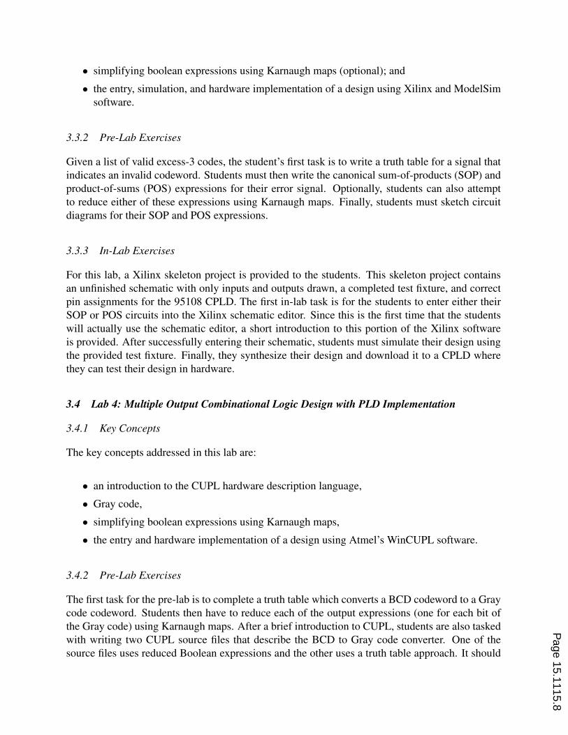
After being given a brief introduction to the three styles of Verilog coding (which is in addition to
similar coverage in lecture), the students complete a truth table describing the active low Boolean
functions for driving all the segments of a seven-segment display in the manner shown in Figure 2.
The input for this truth table is a single four-bit codeword. Students are then tasked to reduce each
of the segment driver expressions using Karnaugh maps. Finally, students write a Verilog module
that implements their seven-segment driver logic.
3.5.3 In-Lab Exercises
The first thing students do when they get to lab is to enter their Verilog module into a skeleton
project that has been preconfigured with a test fixture (that will test the students’ seven-segment
driver logic), correct pin assignments, and a top-level schematic. Students then simulate their
Page 15.1115.9
Figure 2: Desired Hexadecimal Digit Encodings for Seven-Segment Displays
design using the provided test fixture, synthesize it, and download it to the CPLD for hardware
testing.
3.6 Lab 6: Combinational Logic Design with a Decoder
3.6.1 Key Concepts
The key concepts addressed in this lab are:
• incorporating previously defined logic circuits into a larger design;
• the use of a ten-segment LED bar graph; and
• the entry, simulation, and hardware implementation of a design using Xilinx and ModelSim
software.
3.6.2 Pre-Lab Exercises
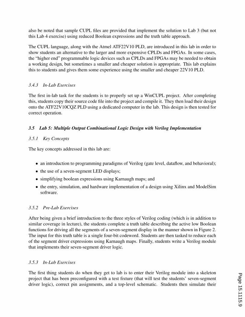
First, students are provided with the truth table for driving a ten-segment bar graph (shown in
Figure 3) using a four-bit codeword. Then, students are instructed to incorporate a 3-to-8 decoder
into a combinational logic design that satisfies the truth table. Because the decoder only has eight
outputs, students also have to come up with additional logic to generate the other two outputs.
����� �����
Figure 3: Ten-Segment LED Bar-Graph
3.6.3 In-Lab Exercises
As was the case with the previous labs, a skeleton project with a test fixture (for testing the students
ten-segment bar graph), correct pin assignments, and a top-level schematic is provided for the
students to use. Thus, their first task is to enter their bar graph design into the provided schematic
file. Students then simulate their design using the provided test fixture, synthesize it, and download
it to the CPLD for hardware testing.
Page 15.1115.10
3.7 Lab 7: Hierarchical Combinational Logic Design
3.7.1 Key Concepts
The key concepts addressed in this lab are:
• hierarchical design techniques;
• the reuse of previous design modules; and
• the entry, simulation, and hardware implementation of a design using Xilinx and ModelSim
software.
3.7.2 Pre-Lab Exercises
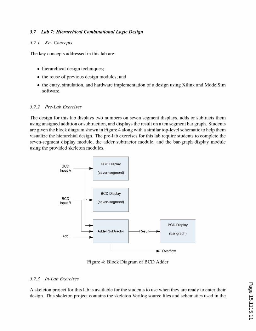
The design for this lab displays two numbers on seven segment displays, adds or subtracts them
using unsigned addition or subtraction, and displays the result on a ten segment bar graph. Students
are given the block diagram shown in Figure 4 along with a similar top-level schematic to help them
visualize the hierarchial design. The pre-lab exercises for this lab require students to complete the
seven-segment display module, the adder subtractor module, and the bar-graph display module
using the provided skeleton modules.
Figure 4: Block Diagram of BCD Adder
3.7.3 In-Lab Exercises
A skeleton project for this lab is available for the students to use when they are ready to enter their
design. This skeleton project contains the skeleton Verilog source files and schematics used in the
Page 15.1115.11
pre-lab, a completed top-level schematic, completed test fixtures for all four modules (the three the
student created and the given top-level module), and the correct pin assignments. After entering
their design into the project, students must simulate each module of their design using the test
fixtures provided. After testing all of the modules, students synthesize their design and download
it to a CPLD for hardware testing.
3.8 Lab 8: Introduction to Sequential Logic Circuit Elements
3.8.1 Key Concepts
The key concepts addressed in this lab are:
• operation of D, JK, and T flip-flops;
• post-fit simulation of a design;
• full schematic entry using Xilinx software;
• behavioral and post-fit simulation using Xilinx and Modelsim software; and
• hardware implementation of a design using Xilinx software.
3.8.2 Pre-Lab Exercises
The pre-lab portion of this lab requires students to provide timing diagrams for a positive edge
triggered D flip-flop with active high output, a positive edge triggered JK flip-flp with active high
output, and a cascade of three positive edge triggered T flip-flops with active high outputs (the
inputs to all of the T flip-flops are tied to a logic high and the clocks are tied to the output of the
previous T flip-flop). Students are provided with the inputs to these flip-flop configurations and are
required to complete the resulting timing diagram.
3.8.3 In-Lab Exercises
A skeleton project with an empty schematic file, a test fixture, and correct pin assignments is
provided to the students. Their first in-lab task is to enter each of three flip-flop configurations
into the single schematic file. This is the first time that students are working without a skeleton
schematic. After entering the schematic, students use the provided test fixture to do a behavioral
simulation on the flip-flops as well as a post-fit simulation. After completing these two simulations,
students synthesize their design and download it to a CPLD for hardware testing.
3.9 Lab 9: Clocked Synchronous State Machine Analysis
3.9.1 Key Concepts
The key concepts addressed in this lab are:
Page 15.1115.12
• clocked synchronous state machine analysis;
• pseudo-noise (PN) sequence generators;
• state diagrams;
• state transition/output tables; and
• the entry, simulation, and hardware implementation of a design using Xilinx and ModelSim
software.
3.9.2 Pre-Lab Exercises
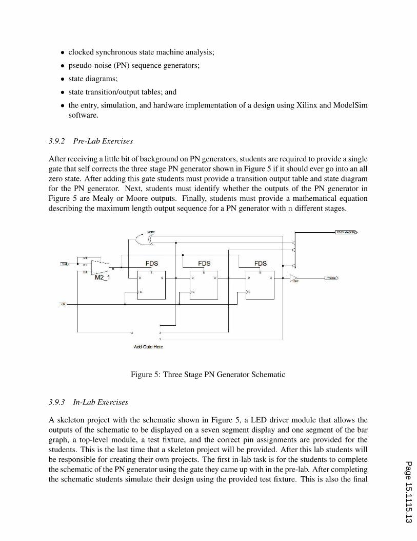
After receiving a little bit of background on PN generators, students are required to provide a single
gate that self corrects the three stage PN generator shown in Figure 5 if it should ever go into an all
zero state. After adding this gate students must provide a transition output table and state diagram
for the PN generator. Next, students must identify whether the outputs of the PN generator in
Figure 5 are Mealy or Moore outputs. Finally, students must provide a mathematical equation
describing the maximum length output sequence for a PN generator with n different stages.
Figure 5: Three Stage PN Generator Schematic
3.9.3 In-Lab Exercises
A skeleton project with the schematic shown in Figure 5, a LED driver module that allows the
outputs of the schematic to be displayed on a seven segment display and one segment of the bar
graph, a top-level module, a test fixture, and the correct pin assignments are provided for the
students. This is the last time that a skeleton project will be provided. After this lab students will
be responsible for creating their own projects. The first in-lab task is for the students to complete
the schematic of the PN generator using the gate they came up with in the pre-lab. After completing
the schematic students simulate their design using the provided test fixture. This is also the final
Page 15.1115.13
time that a test fixture will be provided for the students. After simulation is complete students
synthesize their design and download it to a CPLD for hardware testing.
3.10 Lab 10: Synchronous State Machine Design and Simulation
3.10.1 Key Concepts
The key concepts addressed in this lab are:
• synchronous state machine design;
• test fixture design;
• state diagrams;
• state transition/output tables; and
• the design, entry, simulation, and hardware implementation of a design using Xilinx and
ModelSim software.
3.10.2 Pre-Lab Exercises
This lab requires students to complete a design similar to one that was presented in class. This
design was for a vending machine that accepted dimes and nickels, dispensed a $0.15 product, and
dispensed change when appropriate. In the lecture portion of the class, this design was completed
using a one-hot state machine design. The design that is required for this lab is exactly the same
as the one described in class except that it uses binary coded states instead of one-hot states.
The first pre-lab exercise is for the students to create a transition/output table along with a state
diagram for this design. The next task is to complete a Verilog module for the vending machine.
Then, students must complete a LED driver module which displays the current state of the vending
machine (on a seven-segment display) and whether or not the product and or change was dispensed
(using two of the ten bars on the ten-segment bar graph). Finally, students must complete a test
fixture to test their vending machine module. Students may also optionally write a test fixture to
test their LED driver circuit. Very sparse skeleton code files are provided to help the students in
these tasks.
3.10.3 In-Lab Exercises
This is the first lab in which students are not given any skeleton project. This means that students
will first have to create a new Xilinx project in which to enter their design. After creating this
new project, students add their three completed files to the project. Then, they create a top-level
module that connects the LED driver module to the vending machine module. Once this has been
completed students simulate their design using their own test fixtures. If the design simulates
correctly, students synthesize their design and download it to a CPLD for hardware testing using
the pin assignments described in the lab manual.
Page 15.1115.14
3.11 Lab 11: Clocked Synchronous State Machine Design
3.11.1 Key Concepts
The key concepts addressed in this lab are:
• synchronous state machine design;
• open ended design;
• ASM and ASMD charts;
• state transition tables; and
• the design, entry, simulation, and hardware implementation of a design using Xilinx and
ModelSim software.
3.11.2 Pre-Lab Exercises
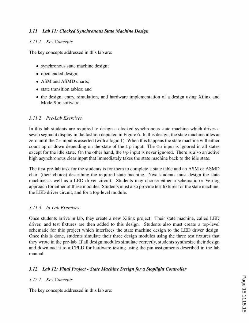
In this lab students are required to design a clocked synchronous state machine which drives a
seven segment display in the fashion depicted in Figure 6. In this design, the state machine idles at
zero until the Go input is asserted (with a logic 1). When this happens the state machine will either
count up or down depending on the state of the Up input. The Go input is ignored in all states
except for the idle state. On the other hand, the Up input is never ignored. There is also an active
high asynchronous clear input that immediately takes the state machine back to the idle state.
The first pre-lab task for the students is for them to complete a state table and an ASM or ASMD
chart (their choice) describing the required state machine. Next students must design the state
machine as well as a LED driver circuit. Students may choose either a schematic or Verilog
approach for either of these modules. Students must also provide test fixtures for the state machine,
the LED driver circuit, and for a top-level module.
3.11.3 In-Lab Exercises
Once students arrive in lab, they create a new Xilinx project. Their state machine, called LED
driver, and test fixtures are then added to this design. Students also must create a top-level
schematic for this project which interfaces the state machine design to the LED driver design.
Once this is done, students simulate their three design modules using the three test fixtures that
they wrote in the pre-lab. If all design modules simulate correctly, students synthesize their design
and download it to a CPLD for hardware testing using the pin assignments described in the lab
manual.
3.12 Lab 12: Final Project - State Machine Design for a Stoplight Controller
3.12.1 Key Concepts
The key concepts addressed in this lab are:
Page 15.1115.15
Sequence for Sequence for
Up=0 Up=1
Seven Seg Display Description Seven Seg Display
Idle state, displayed as
shown. Return here af-
ter ninth step as well as
when Clear=1 is de-
tected.
First step after Go=1
sensed; displayed as
shown.
Second step after Go=1
sensed; displayed as
shown.
Third step after Go=1
sensed; displayed as
shown.
Fourth step after Go=1
sensed; displayed as
shown.
Fifth step after Go=1
sensed; displayed as
shown.
Sixth step after Go=1
sensed; displayed as
shown.
Seventh step after Go=1
sensed; displayed as
shown.
Eighth step after Go=1
sensed; displayed as
shown.
Ninth step after Go=1
sensed; displayed as
shown. Return to idle
state at next tick of
clock.
Figure 6: Desired “light” Signal Pattern Sequence
Page 15.1115.16
• synchronous state machine design;
• large open ended design;
• ASM and ASMD charts;
• state transition tables; and
• the design, entry, simulation, and hardware implementation of a design using Xilinx and
ModelSim software.
3.12.2 Pre-Lab Exercises
As the final lab exercise for EE2390, it is designed to take two weeks to complete. There are also
four acceptable levels of completion. Levels 1-4 correspond to maximum possible grades of 75%,
85%, 100%, and 110% respectively. Students are encouraged to start at level one and work their
way up to level four, saving their work as they go. They are not required to go beyond level 1, but
essentially all students do. Pre-lab exercises are not be graded at the beginning of this lab exercise,
as the students are told they should by now be responsible for coming to lab fully prepared. It is
up to the student to make sure that their design is documented to the given specifications.
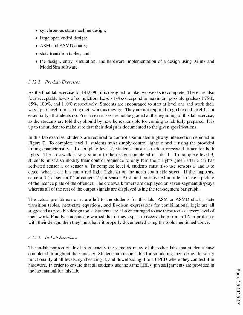
In this lab exercise, students are required to control a simulated highway intersection depicted in
Figure 7. To complete level 1, students must simply control lights X and Z using the provided
timing characteristics. To complete level 2, students must also add a crosswalk timer for both
lights. The crosswalk is very similar to the design completed in lab 11. To complete level 3,
students must also modify their control sequence to only turn the X lights green after a car has
activated sensor C or sensor A. To complete level 4, students must also use sensors B and D to
detect when a car has run a red light (light X) on the north south side street. If this happens,
camera U (for sensor D) or camera V (for sensor B) should be activated in order to take a picture
of the licence plate of the offender. The crosswalk timers are displayed on seven-segment displays
whereas all of the rest of the output signals are displayed using the ten-segment bar graph.
The actual pre-lab exercises are left to the students for this lab. ASM or ASMD charts, state
transition tables, next-state equations, and Boolean expressions for combinational logic are all
suggested as possible design tools. Students are also encouraged to use these tools at every level of
their work. Finally, students are warned that if they expect to receive help from a TA or professor
with their design, then they must have it properly documented using the tools mentioned above.
3.12.3 In-Lab Exercises
The in-lab portion of this lab is exactly the same as many of the other labs that students have
completed throughout the semester. Students are responsible for simulating their design to verify
functionality at all levels, synthesizing it, and downloading it to a CPLD where they can test it in
hardware. In order to ensure that all students use the same LEDs, pin assignments are provided in
the lab manual for this lab.
Page 15.1115.17
�
�
�
�
�
�
�
�����
����
�����
����
Figure 7: Intersection Used for Lab 12
4 Conclusion
The set of EE2390 laboratory exercises described above was created by a former EE2390 student
who is now a graduate student. This is an example of our “By Students, For Students” method,
which leverages a student’s relatively recent memory of what what were some of the biggest hur-
dles for a particular course. Feedback from EE2390 TAs who taught both the previous version
of the lab and this new version was interesting. Overall, the new lab exercises appeared to be
“harder” and most of the individual lab grades were thus lower. However, on the final lab exercise
in which the students are given an open-ended realistic design challenge, the results were much
better. Thus we tentatively conclude that the more difficult lab exercises prepared the students
better for open-ended design problems.
After analyzing the topic coverage of these lab exercises along with the content of related higher-
level elective courses (such as Verilog HDL and Computer Architecture) that are being offered at
the University of Wyoming, we also believe that a new course in design verification techniques
would be a useful addition to the curriculum. This course would teach various verification tech-
niques, test planning, code coverage, and other similar concepts that are used by engineers in
industry today.
We encourage educators to give the “By Students, For Students” method a try; we have found it to
be both successful from a pedagogical standpoint but also immensely popular with students.
Page 15.1115.18
References
[1] M. A. Yoder, J. H. McClellan, and R. W. Schafer, “Experiences in teaching DSP first in the ECE
curriculum,” in Proceedings of the 1997 ASEE Annual Conference, June 1997, paper 1220-06.
[2] R. G. Jacquot, J. C. Hamann, J. W. Pierre, and R. F. Kubichek, “Teaching digital filter design using
symbolic and numeric features of MATLAB,” ASEE Comput. Educ. J., vol. VII, no. 1, pp. 8–11, January–
March 1997.
[3] C. H. G. Wright and T. B. Welch, “Teaching DSP concepts using MATLAB and the TMS320C31 DSK,”
in Proceedings of the IEEE International Conference on Acoustics, Speech, and Signal Processing, Mar.
1999, paper 1778.
[4] J. W. Pierre, F. K. Tuffner, J. R. Anderson, D. L. Whitman, A. H. M. S. Ula, R. F. Kubichek, C. H. G.
Wright, S. F. Barrett, J. J. Cupal, and J. C. Hamann, “A one-credit hour hands-on introductory course in
electrical and computer engineering using a variety of topic modules,” IEEE Trans. Educ., vol. 52, May
2009, in press.
[5] S. F. Barrett, D. Whitman, R. Kubichek, J. Pierre, S. Muknahallipatna, and C. H. G. Wright, “Embedded
systems design: responding to the challenge,” in Proceedings of the 2009 ASEE Annual Conference,
Austin, TX, June 2009.
[6] M. M. Mano and M. D. Ciletti, Digital Design, 4th ed. Prentice Hall, 2007.
[7] K. Morris, “Tilting at tech market windmills,” FPGA and Programmable Logic Journal, March 2004.
[8] ——, “Who’s winning in FPGAs II,” FPGA and Structured ASIC Journal, November 2008.
[9] C. H. G. Wright, J. C. Hamann, and D. D. McCarthy, EE/COSC 2390 Digital Systems Design Labora-
tory Manual, University of Wyoming, Laramie, WY 82071, April 2009.
Page 15.1115.19