Embed Size (px)
Citation preview
Santa Clara, CA, USA, August 2010 1
STT-RAM:Advantages & Applications
Farhad TabriziGrandis, Inc.
Flash Memory SummitAugust 19th, 2010
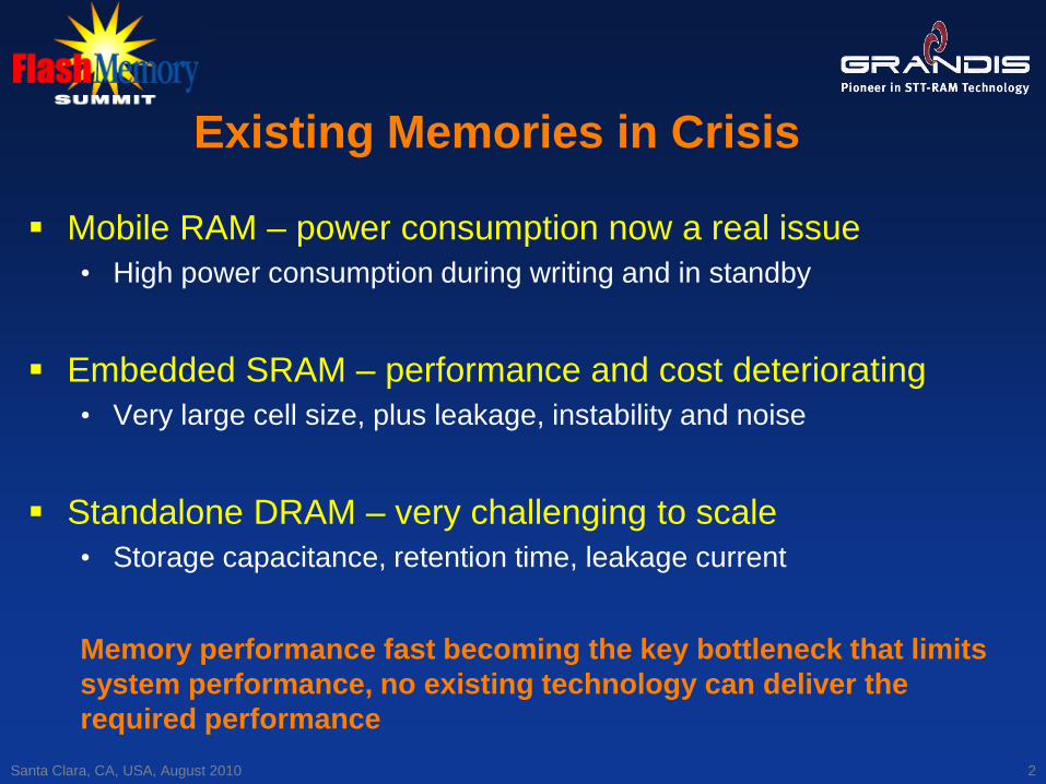
Existing Memories in Crisis
Mobile RAM – power consumption now a real issue• High power consumption during writing and in standby
Embedded SRAM – performance and cost deteriorating• Very large cell size, plus leakage, instability and noise
Standalone DRAM – very challenging to scale• Storage capacitance, retention time, leakage current
Memory performance fast becoming the key bottleneck that limits system performance, no existing technology can deliver the required performance
2Santa Clara, CA, USA, August 2010
Santa Clara, CA, USA, August 2010 3
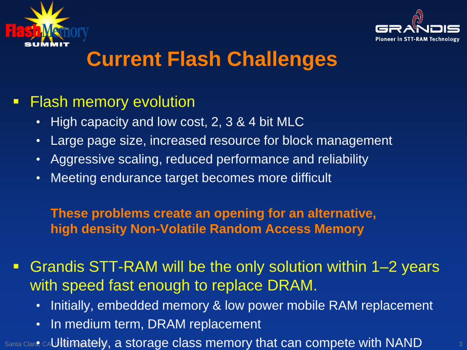
Current Flash Challenges
Flash memory evolution • High capacity and low cost, 2, 3 & 4 bit MLC• Large page size, increased resource for block management• Aggressive scaling, reduced performance and reliability• Meeting endurance target becomes more difficult
These problems create an opening for an alternative,high density Non-Volatile Random Access Memory
Grandis STT-RAM will be the only solution within 1–2 years with speed fast enough to replace DRAM.• Initially, embedded memory & low power mobile RAM replacement• In medium term, DRAM replacement• Ultimately, a storage class memory that can compete with NAND
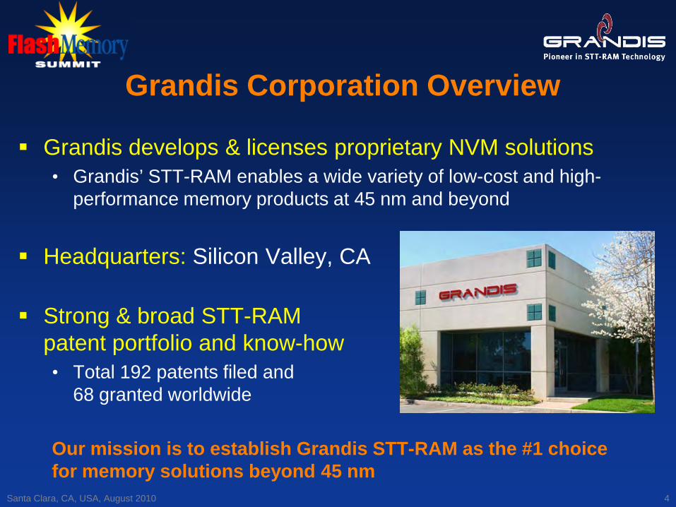
Grandis Corporation Overview
Grandis develops & licenses proprietary NVM solutions• Grandis’ STT-RAM enables a wide variety of low-cost and high-
performance memory products at 45 nm and beyond
Headquarters: Silicon Valley, CA
Strong & broad STT-RAMpatent portfolio and know-how• Total 192 patents filed and
68 granted worldwide
Our mission is to establish Grandis STT-RAM as the #1 choicefor memory solutions beyond 45 nm
Santa Clara, CA, USA, August 2010 4
Santa Clara, CA, USA, August 2010 5
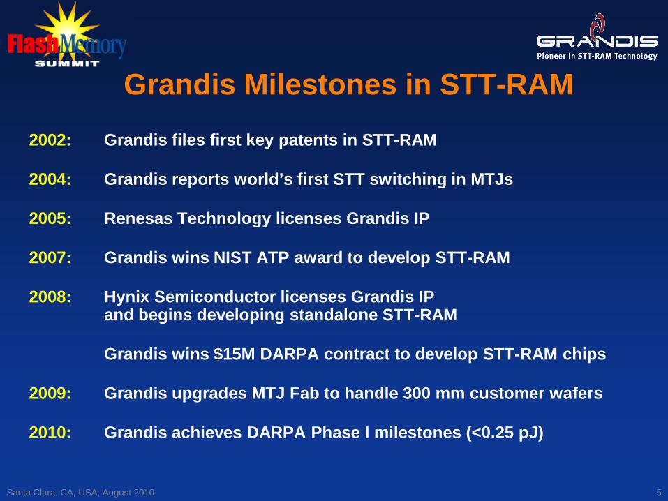
Grandis Milestones in STT-RAM2002: Grandis files first key patents in STT-RAM
2004: Grandis reports world’s first STT switching in MTJs
2005: Renesas Technology licenses Grandis IP
2007: Grandis wins NIST ATP award to develop STT-RAM
2008: Hynix Semiconductor licenses Grandis IPand begins developing standalone STT-RAM
Grandis wins $15M DARPA contract to develop STT-RAM chips
2009: Grandis upgrades MTJ Fab to handle 300 mm customer wafers
2010: Grandis achieves DARPA Phase I milestones (<0.25 pJ)
Santa Clara, CA, USA, August 2010 6
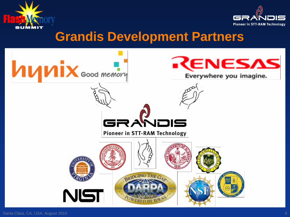
Grandis Development Partners
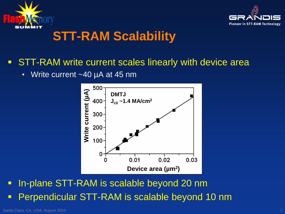
STT-RAM Scalability
STT-RAM write current scales linearly with device area• Write current ~40 µA at 45 nm
In-plane STT-RAM is scalable beyond 20 nm Perpendicular STT-RAM is scalable beyond 10 nm
Santa Clara, CA, USA, August 2010 7
Device area (µm2)
Writ
e cu
rren
t (µA
)DMTJJc0 ~1.4 MA/cm2
Latest Advances in Write Energy
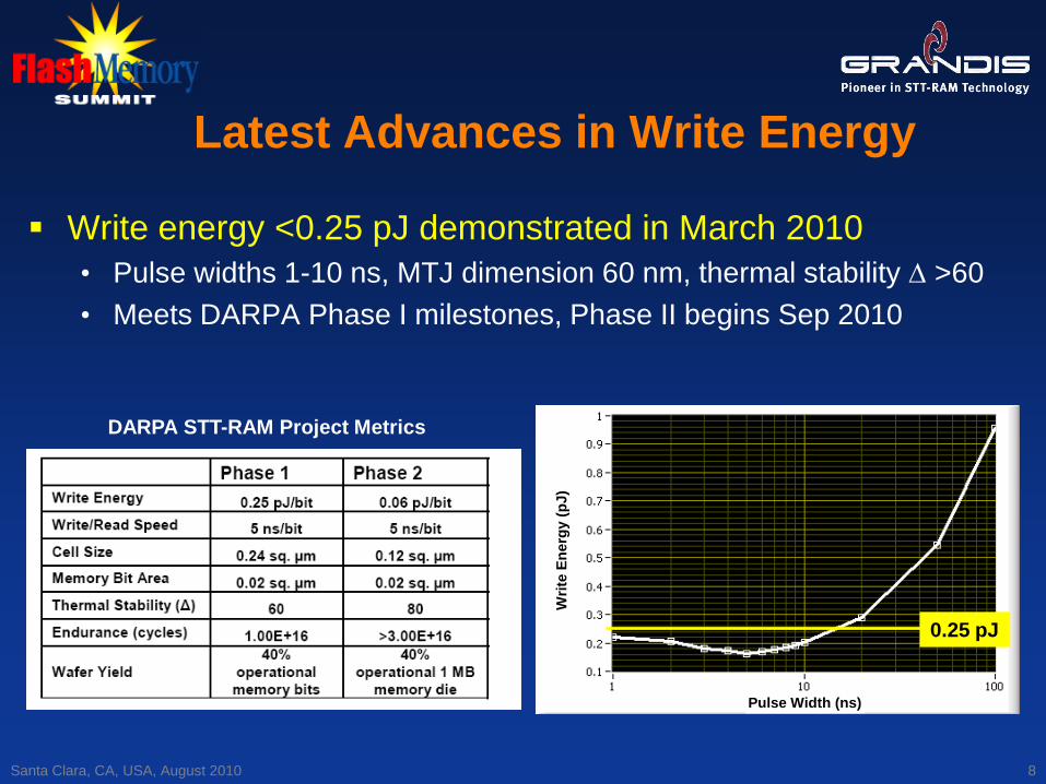
Write energy <0.25 pJ demonstrated in March 2010• Pulse widths 1-10 ns, MTJ dimension 60 nm, thermal stability ∆ >60• Meets DARPA Phase I milestones, Phase II begins Sep 2010
Santa Clara, CA, USA, August 2010 8
DARPA STT-RAM Project Metrics
0.25 pJ
Pulse Width (ns)
Writ
e En
ergy
(pJ)
STT-RAM Minimum Cell Size
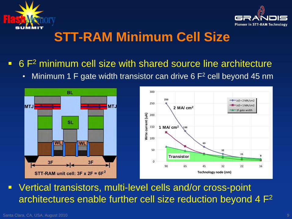
6 F2 minimum cell size with shared source line architecture• Minimum 1 F gate width transistor can drive 6 F2 cell beyond 45 nm
Vertical transistors, multi-level cells and/or cross-point architectures enable further cell size reduction beyond 4 F2
Santa Clara, CA, USA, August 2010 9
250
130
63
32
158
0
50
100
150
200
250
300
90 65 45 32 22 16
Technology node (nm)
Wrt
e cu
rren
t (u
A)
Jc0 = 2 MA/cm2
Jc0 = 1 MA/cm2
1F gate width2 MA/cm2
1 MA/cm2
Transistor
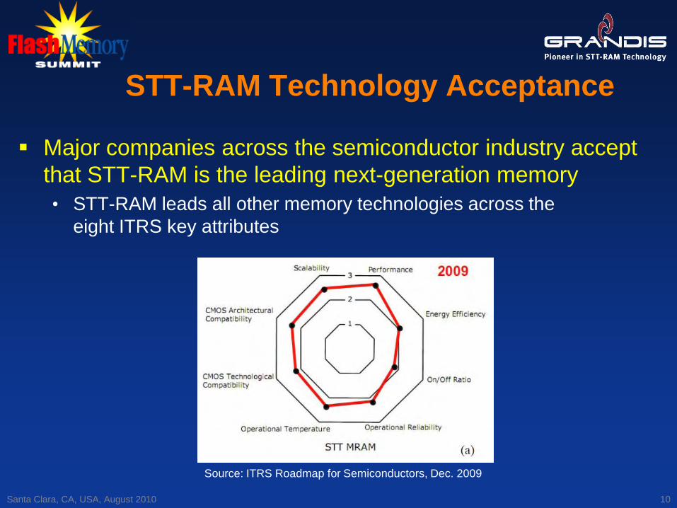
STT-RAM Technology Acceptance
Major companies across the semiconductor industry accept that STT-RAM is the leading next-generation memory• STT-RAM leads all other memory technologies across the
eight ITRS key attributes
Source: ITRS Roadmap for Semiconductors, Dec. 2009
Santa Clara, CA, USA, August 2010 10
Santa Clara, CA, USA, August 2010 11
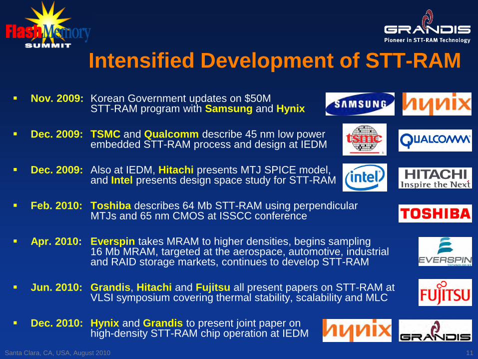
Intensified Development of STT-RAM Nov. 2009: Korean Government updates on $50M
STT-RAM program with Samsung and Hynix
Dec. 2009: TSMC and Qualcomm describe 45 nm low powerembedded STT-RAM process and design at IEDM
Dec. 2009: Also at IEDM, Hitachi presents MTJ SPICE model,and Intel presents design space study for STT-RAM
Feb. 2010: Toshiba describes 64 Mb STT-RAM using perpendicularMTJs and 65 nm CMOS at ISSCC conference
Apr. 2010: Everspin takes MRAM to higher densities, begins sampling16 Mb MRAM, targeted at the aerospace, automotive, industrialand RAID storage markets, continues to develop STT-RAM
Jun. 2010: Grandis, Hitachi and Fujitsu all present papers on STT-RAM atVLSI symposium covering thermal stability, scalability and MLC
Dec. 2010: Hynix and Grandis to present joint paper onhigh-density STT-RAM chip operation at IEDM
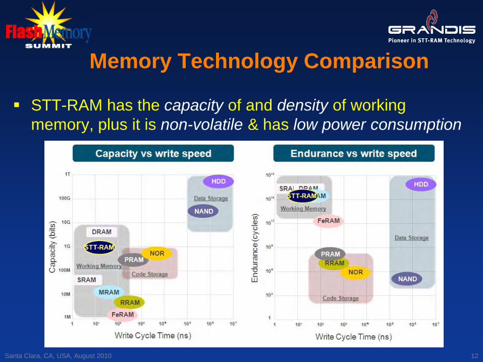
Memory Technology Comparison
Santa Clara, CA, USA, August 2010 12
STT-RAM has the capacity of and density of working memory, plus it is non-volatile & has low power consumption
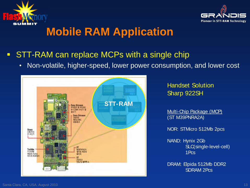
Mobile RAM Application
STT-RAM can replace MCPs with a single chip• Non-volatile, higher-speed, lower power consumption, and lower cost
Santa Clara, CA, USA, August 2010 13
Handset SolutionSharp 922SH
Multi-Chip Package (MCP)(ST M39PNRA2A)
NOR: STMicro 512Mb 2pcs
NAND: Hynix 2Gb SLC(single-level-cell)1Pcs
DRAM: Elpida 512Mb DDR2 SDRAM 2Pcs
STT-RAM
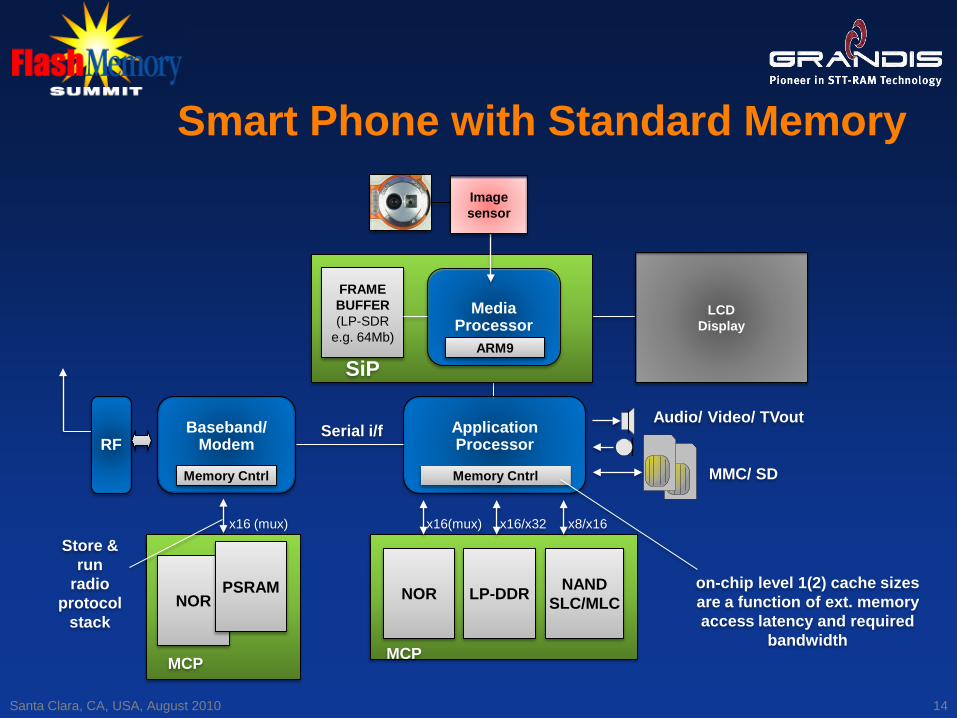
Smart Phone with Standard Memory
x16 (mux)
Baseband/Modem
Application ProcessorRF
MMC/ SD
Audio/ Video/ TVout
Memory Cntrl
NORPSRAM
MCP
LP-DDR
x16/x32
NANDSLC/MLC
MCP
NOR
Memory Cntrl
x16(mux) x8/x16
Serial i/f
Store & run
radio protocol
stack
on-chip level 1(2) cache sizes are a function of ext. memory access latency and required
bandwidth
Media Processor
FRAMEBUFFER(LP-SDR
e.g. 64Mb)
SiP
LCDDisplay
ARM9
Imagesensor
Santa Clara, CA, USA, August 2010 14
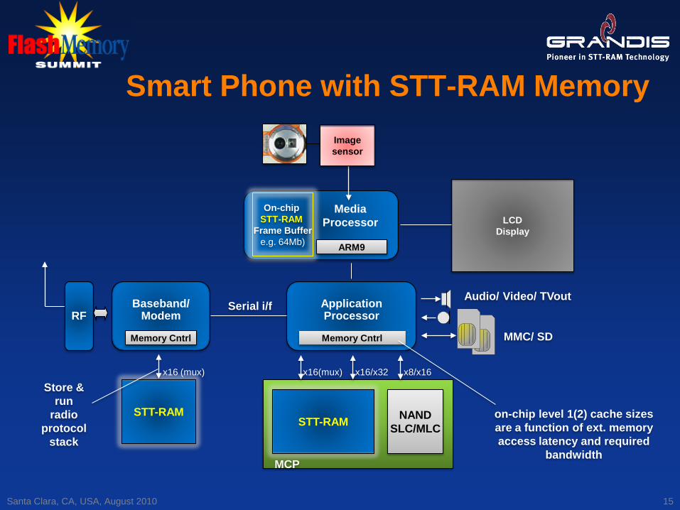
Smart Phone with STT-RAM Memory
x16 (mux)
Baseband/Modem
Application ProcessorRF
MMC/ SD
Audio/ Video/ TVout
Memory Cntrl
STT-RAM
x16/x32
NANDSLC/MLC
MCP
STT-RAM
Memory Cntrl
x16(mux) x8/x16
Serial i/f
Store & run
radio protocol
stack
on-chip level 1(2) cache sizes are a function of ext. memory access latency and required
bandwidth
On-chip STT-RAM
Frame Buffere.g. 64Mb)
LCDDisplay
ARM9
Imagesensor
Media Processor
Santa Clara, CA, USA, August 2010 15
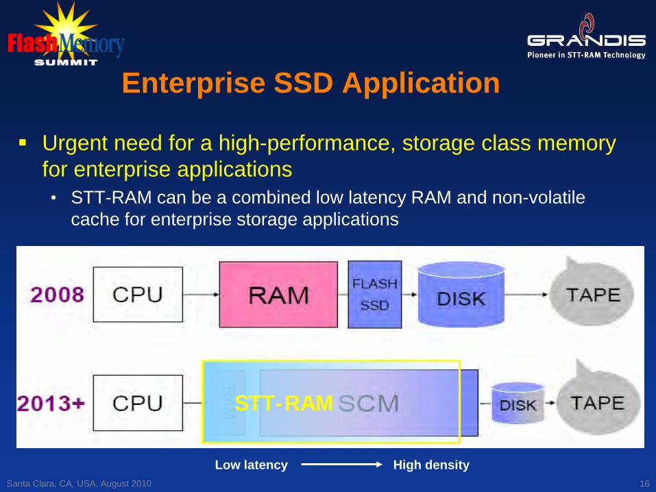
Enterprise SSD Application
Urgent need for a high-performance, storage class memory for enterprise applications• STT-RAM can be a combined low latency RAM and non-volatile
cache for enterprise storage applications
Santa Clara, CA, USA, August 2010 16
Low latency High density
STT-RAM
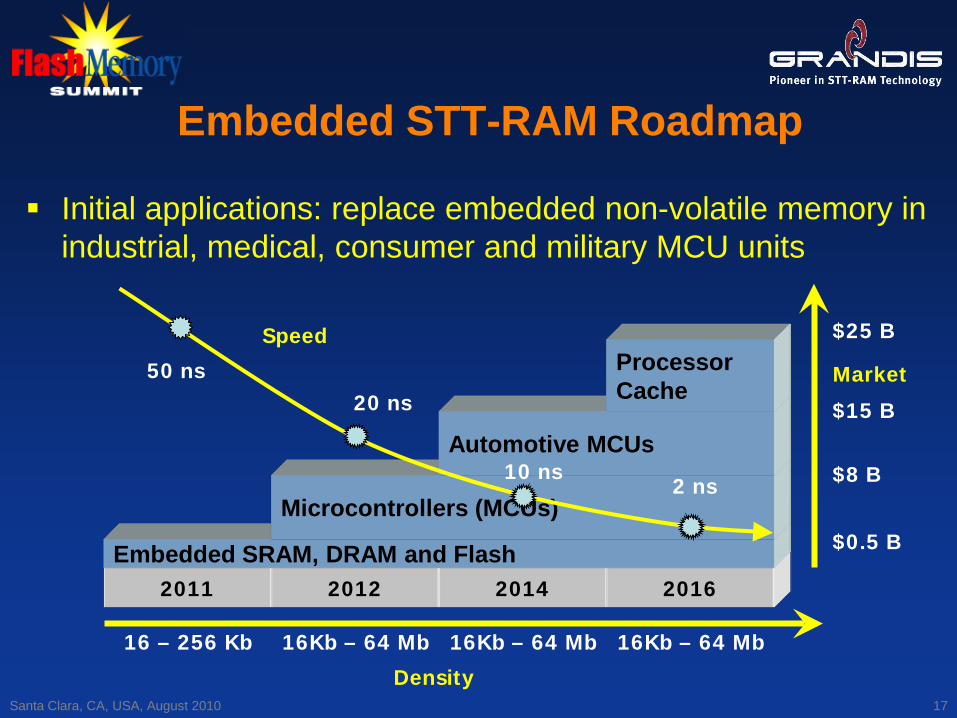
Embedded STT-RAM Roadmap
Initial applications: replace embedded non-volatile memory in industrial, medical, consumer and military MCU units
Santa Clara, CA, USA, August 2010 17
2011 2012 2014 2016
Embedded SRAM, DRAM and Flash
Microcontrollers (MCUs)
Automotive MCUs
Market
$0.5 B
$15 B
$25 B
50 ns20 ns
10 ns2 ns
16 – 256 Kb 16Kb – 64 Mb 16Kb – 64 Mb 16Kb – 64 Mb
Density
SpeedProcessor Cache
$8 B
2010 2012 2014 2016
Mobile MCP(NOR + NAND + DRAM)
DRAM
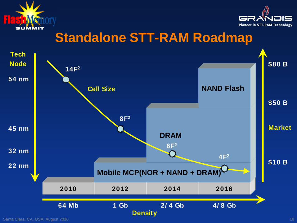
Standalone STT-RAM RoadmapTechNode
Market
$10 B
$50 B
$80 B14F2
54 nm
45 nm8F2
6F2
4F232 nm
22 nm
64 Mb 1 Gb 2/4 Gb 4/8 GbDensity
Cell Size NAND Flash
Santa Clara, CA, USA, August 2010 18
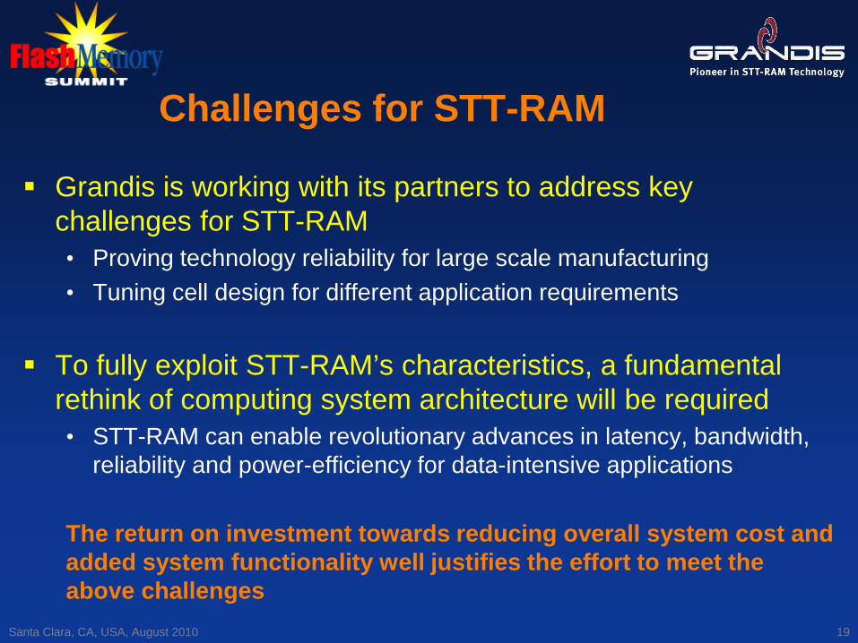
Challenges for STT-RAM
Grandis is working with its partners to address key challenges for STT-RAM• Proving technology reliability for large scale manufacturing• Tuning cell design for different application requirements
To fully exploit STT-RAM’s characteristics, a fundamental rethink of computing system architecture will be required• STT-RAM can enable revolutionary advances in latency, bandwidth,
reliability and power-efficiency for data-intensive applications
The return on investment towards reducing overall system cost and added system functionality well justifies the effort to meet the above challenges
Santa Clara, CA, USA, August 2010 19
Summary
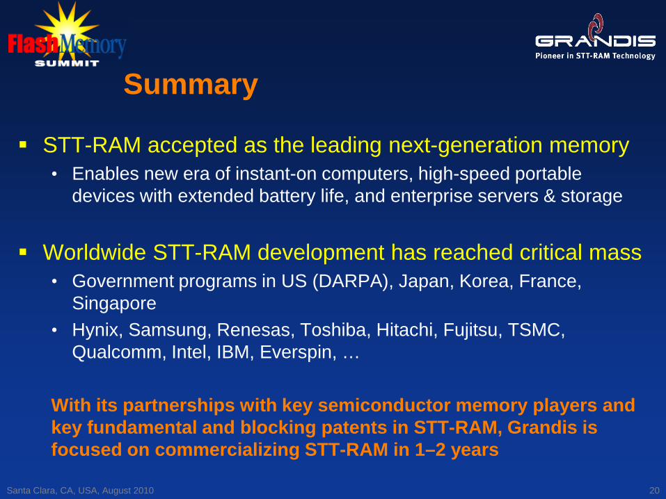
STT-RAM accepted as the leading next-generation memory• Enables new era of instant-on computers, high-speed portable
devices with extended battery life, and enterprise servers & storage
Worldwide STT-RAM development has reached critical mass• Government programs in US (DARPA), Japan, Korea, France,
Singapore• Hynix, Samsung, Renesas, Toshiba, Hitachi, Fujitsu, TSMC,
Qualcomm, Intel, IBM, Everspin, …
With its partnerships with key semiconductor memory players and key fundamental and blocking patents in STT-RAM, Grandis is focused on commercializing STT-RAM in 1–2 years
Santa Clara, CA, USA, August 2010 20

Santa Clara, CA, USA, August 2010 21
Please visitwww.GrandisInc.com
for more information