Embed Size (px)
Citation preview
NANO EXPRESS Open Access
Structural and optical characterizations of InPBithin films grown by molecular beam epitaxyYi Gu1, Kai Wang1, Haifei Zhou1, Yaoyao Li1, Chunfang Cao1, Liyao Zhang1, Yonggang Zhang1, Qian Gong1*
and Shumin Wang1,2*
Abstract
InPBi thin films have been grown on InP by gas source molecular beam epitaxy. A maximum Bi composition of2.4% is determined by Rutherford backscattering spectrometry. X-ray diffraction measurements show goodstructural quality for Bi composition up to 1.4% and a partially relaxed structure for higher Bi contents. The bandgapwas measured by optical absorption, and the bandgap reduction caused by the Bi incorporation was estimated tobe about 56 meV/Bi%. Strong and broad photoluminescence signals were observed at room temperature forsamples with xBi < 2.4%. The PL peak position varies from 1.4 to 1.9 μm, far below the measured InPBi bandgap.
Keywords: InPBi; HRXRD; Absorption; Photoluminescence; Molecular beam epitaxy
BackgroundGroup III-V semiconductors containing small amountsof bismuth (Bi), popularly known as ‘dilute bismide,’attracted great attention in the past decade. Bismuth isthe largest and the heaviest group V element with itsisoelectronic energy level that resides in the valenceband of most III-V materials. Incorporation of a smallamount of Bi atoms in a common III-V compound is ex-pected to lead to a large bandgap reduction [1] andstrong spin-orbit splitting [2]. This provides a new de-gree of freedom to engineering the band structure for po-tential optoelectronic and electronic device applications.Under such conditions, it is expected that troublesomehot-hole-induced Auger recombination and inter-valenceband absorption (IVBA) processes can be suppressed lead-ing to high efficiency and temperature insensitive lasersfor optical communications [3]. Most published literaturesso far focus on growth and material properties of GaAsBiwith improving quality, making GaAsBi closer to deviceapplications. GaAsBi light-emitting diodes (LEDs) [4] andoptically pumped [5] and electrically injected [6] laser di-odes have been demonstrated recently.
Group III-V semiconductor phosphides are importantmaterials for optoelectronic devices working at visibleand near-infrared wavelength range [7,8]. The incorpor-ation of Bi into InP can further extend transition wave-lengths for optoelectronic devices with aforementionedimproved device performances as a result of the sup-pressed Auger recombination and IVBA processes. Berdinget al. theoretically compared InPBi, InAsBi, InSbBi, andHgCdTe, and pointed out that InPBi was much more ro-bust than the others, thus making it as a promising candi-date for infrared applications. However, their calculationsalso showed that InPBi was very difficult to synthesize dueto a larger miscibility gap than that of InAsBi and InSbBi[9]. So far, a few works on the optical studies of InP/Biwhere the incorporated Bi is only in the doping level[10,11] were reported. The spectroscopy reveals rich sharptransitions at energy levels close to the InP bandgap at lowtemperatures.In this work, we investigate the structural and optical
properties of InPBi with Bi composition in the range of0.6% to 2.4%. The Bi-induced bandgap reduction of around56 meV/Bi% is obtained. Strong and broad photolumines-cence (PL) signals have been observed at transition energymuch smaller than the InPBi bandgap.* Correspondence: [email protected]; [email protected]
1State Key Laboratory of Functional Materials for Informatics, ShanghaiInstitute of Microsystem and Information Technology, Chinese Academy ofSciences, Shanghai 200050, China2Department of Microtechnology and Nanoscience, Chalmers University ofTechnology, Gothenburg 41296, Sweden
© 2014 Gu et al.; licensee Springer. This is an Open Access article distributed under the terms of the Creative CommonsAttribution License (http://creativecommons.org/licenses/by/2.0), which permits unrestricted use, distribution, and reproductionin any medium, provided the original work is properly cited.
Gu et al. Nanoscale Research Letters 2014, 9:24http://www.nanoscalereslett.com/content/9/1/24
MethodsThe samples were grown on (100) semi-insulating InPsubstrates by V90 gas source molecular beam epitaxy(GSMBE). Elemental In and Bi and P2 cracked from phos-phine were applied. After the surface oxide desorption ofInP substrate at 524°C, a 75-nm undoped InP buffer wasgrown at 474°C, the normal growth temperature of InP.Then the growth temperature was decreased significantlyfor InPBi growth. Both the Bi/P ratio and the growthtemperature were adjusted to achieve InPBi with variousBi compositions. The thickness of the InPBi epi-layers waskept around 430 nm. An InP reference sample was alsogrown at the low temperature.After the growth, the Bi compositions were determined
by Rutherford backscattering spectrometry (RBS) with2.275 MeV 4He2+ ions. The structural qualities were char-acterized by a Philips X’pert MRD high-resolution x-raydiffractometer (HRXRD) equipped with a four-crystal Ge(220) monochromator (Philips, Amsterdam, Netherlands).The PL and absorption spectra were measured using aNicolet Magna 860 Fourier transform infrared (FTIR) spec-trometer (Thermo Fisher Scientific Inc., Waltham, MA,USA), in which a liquid-nitrogen cooled InSb detector anda CaF2 beam splitter were used. A diode-pumped solid-state (DPSS) laser (λ = 532 nm) was used as the excitationsource for PL measurements, and the double modulationmode was used to eliminate the mid-infrared backgroundradiation beyond 2 μm [12]. For the low-temperaturePL measurements, the samples were mounted into acontinuous-flow helium cryostat, and the temperaturewas controlled from 8 to 300 K by a Lake Shore 330temperature controller (Lake Shore Cryotronics, Inc.,Westerville, OH, USA).
Results and discussionsThe Bi incorporation was examined by RBS measurementsas shown in the inset of Figure 1, and the Bi concentra-tions were deduced from the simulations. For all the InPBisamples with various Bi compositions, two main peaks areobserved in the HRXRD ω/2θ scan curves in the (004) re-flection direction as shown in Figure 1. The narrower peakwith a stronger intensity corresponds to the InP bufferlayer and substrate for each sample, while the peak on theleft side corresponds to InPBi epi-layer. Asymmetric (224)reflections were performed to obtain the exact lattice mis-match between the epi-layer and the substrate. Then thestrain relaxation and lattice constant of each sample wereobtained, assuming the same Poisson ratio for InPBi andInP. The relaxation degree increased to about 35% for thesample with the highest Bi content, while the sample withthe least Bi composition is nearly fully strained. As the Bicontent increases, the HRXRD peak intensity of InPBi isreduced and the peak width increases from about 46 to580 arcsec due to the partial lattice relaxation. Using the
Vegard’s law and the lattice constant value of InP 5.8688 Å,the average lattice constant of InBi binary alloy is calculatedto be 7.292 Å, which is much larger than the former reportsof 6.639 Å [13], 6.686 Å [14], or 7.024 Å [15].Figure 2 shows square of absorption coefficient of InPBi
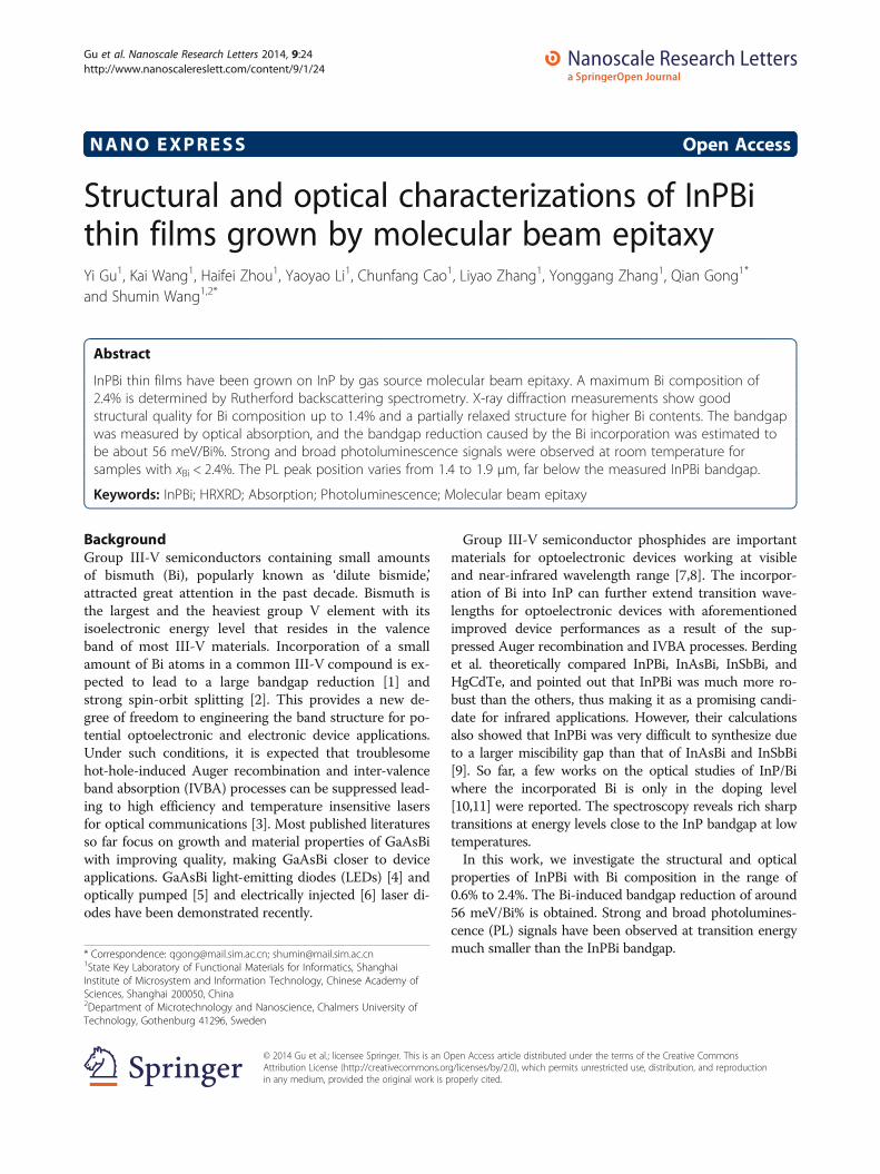
films with various Bi compositions as a function of photonenergy at room temperature (RT). The band edge of the
Figure 1 HRXRD (004) scan curves of InPBi samples withvarious Bi compositions. The inset shows the RBS spectrum fromthe InPBi film with xBi = 1.4% (solid line). The simulated spectrumand the contributions of Bi, In, P are also contained (dashed lines).
Figure 2 Square of absorption coefficient of InPBi samples.Square of absorption coefficient of InPBi samples with various Bicompositions as a function of photon energy at room temperature.
Gu et al. Nanoscale Research Letters 2014, 9:24 Page 2 of 5http://www.nanoscalereslett.com/content/9/1/24
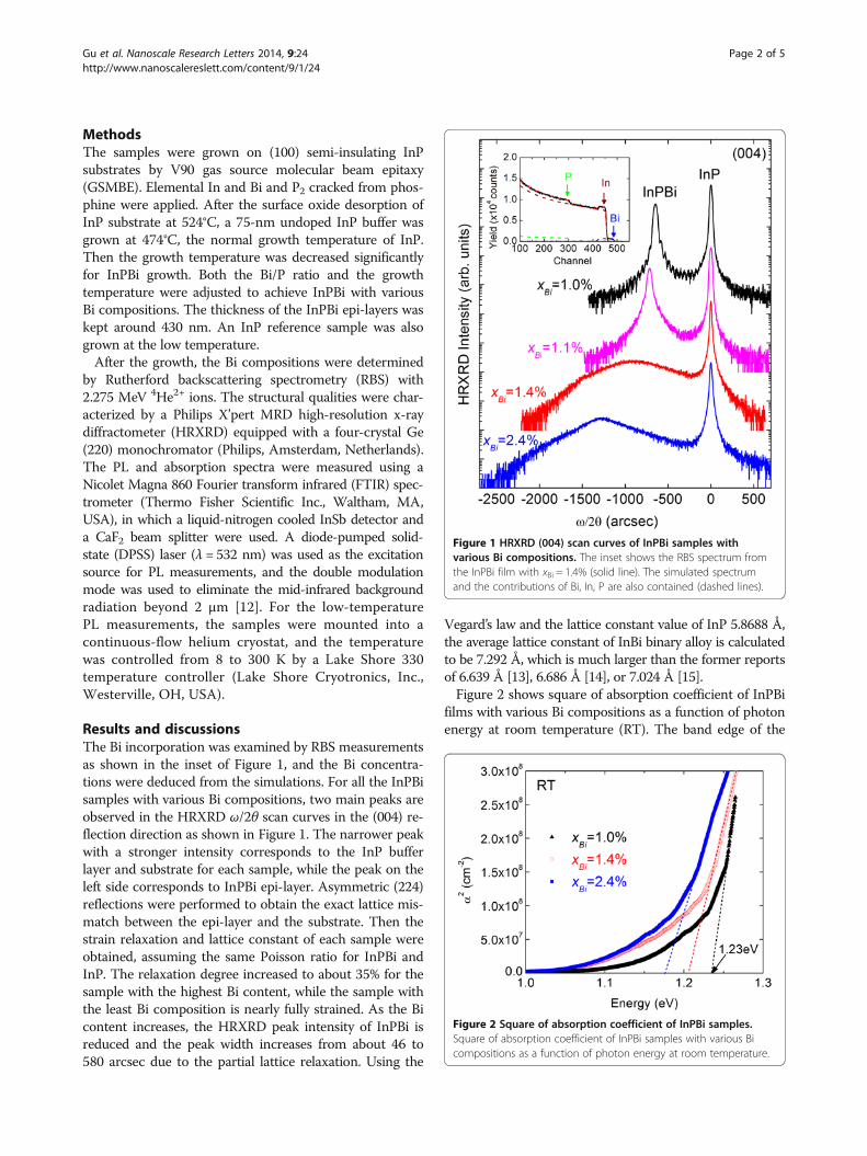
InPBi film shifts to longer wavelengths as the Bi compos-ition increases, revealing a reduction of the bandgap en-ergy. The bandgap value is obtained from the linearextrapolation of the rising part for each sample [16] andshown in Figure 3, where the error bars are also labeled.By using the linear fitting of the experimental data, the Bi-induced bandgap reduction of about 56 meV/%Bi is ob-tained, which is smaller than the value of 88 meV/%Bi forGaAsBi [1] close to 55 meV/%Bi for InAsBi [15], but largerthan 23 meV/%Bi for InSbBi [17].Figure 4 shows the PL spectra of InPBi films with Bi
composition xBi from 0.6% to 2.4% at RT. Strong andbroad PL peaks are observed for the samples, except forthe sample with the highest Bi composition. The PL peakenergy first shifts from 0.9 eV (1.4 μm) to 0.65 eV(1.9 μm), when xBi increases from 0.6% to 1.0%, and thenturns back for the samples with a higher xBi, but in allcases far from the bandgap energy. On the other hand, theInP reference sample only shows one PL peak at around1.34 eV (0.93 μm) corresponding to the band-to-bandtransition. The InPBi sample with xBi = 0.6% shows a verybroad PL envelope from about 1.2 eV (1 μm) to 0.5 eV(2.5 μm), with a peak wavelength at around 0.9 eV(1.4 μm). The sample with xBi = 1.0% reveals the longestPL wavelength (peak at about 1.9 μm) and the strongestintensity. As the Bi composition further increases, the PLwavelength starts to blueshift and the PL intensity de-creases. For the sample with 1.4% Bi, the PL peak is blue-shifted to around 0.73 eV (1.7 μm) and the PL intensity isweakened to about 1/40 of the sample with the strongestPL intensity. No PL signal was detected for the samplewith 2.4% Bi. The clear RT PL signals far from the InPBibandgap are unexpected. The Bi incorporation into GaAs
was found to induce shallow localized states associatedwith Bi clusters above the top of the GaAs valence banddue to the valence band anticrossing interaction, thuscausing the red shift of PL [1,18]. In addition, the Bi in InPwith a doping level was found to act as isoelectronic im-purities and revealed rich spectroscopic information nearthe bandgap of InP (1.3 to 1.4 eV) at low temperatures[10,11]. However, the effects of cluster localization andisoelectronic impurities both introduce the PL peak redshift near the InP bandgap energy, in contrast to the PLsignals observed from the middle of the bandgap.To learn more about the PL signals, PL measurements
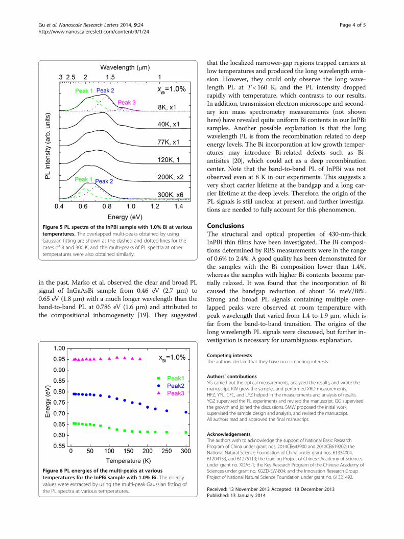
in the temperature range of 8 to 300 K were conducted.Figure 5 shows PL spectra at various temperatures forInPBi with xBi = 1.0%. The PL peak intensity is only en-hanced about six times when the temperature decreasesfrom 300 to 8 K. The PL spectra seem to contain multi-peaks, so Gaussian fitting was implemented to extractthose multi-peaks and their temperatures dependence wasshown in Figure 6. Three overlapped peaks are identifiedin the PL spectra at T < 180 K, whereas at T > 180 K thepeak at around 0.95 eV disappears and the other twopeaks are overlapped. The peak energies labeled peaks 1and 2 red shifted about 82 and 108 meV, respectively,when the temperature increases from 8 to 300 K, compar-able to the red-shifted value of 71 meV for the InP refer-ence sample. However, the peak energies labeled peak 3are almost constant at around 0.95 eV at various tempera-tures. To our knowledge, the PL signal of dilute bismidesfar from the band-to-band transition was scarcely reported
Figure 3 Bandgap energy of InPBi measured from absorptionspectra as a function of Bi composition. The error bars of theexperimental data are labeled. The solid line is the fitting line of theexperimental data.
Figure 4 PL spectra of InPBi films with various Bi compositionsat RT. The PL spectrum of InP reference sample is also shown.
Gu et al. Nanoscale Research Letters 2014, 9:24 Page 3 of 5http://www.nanoscalereslett.com/content/9/1/24
in the past. Marko et al. observed the clear and broad PLsignal of InGaAsBi sample from 0.46 eV (2.7 μm) to0.65 eV (1.8 μm) with a much longer wavelength than theband-to-band PL at 0.786 eV (1.6 μm) and attributed tothe compositional inhomogeneity [19]. They suggested
that the localized narrower-gap regions trapped carriers atlow temperatures and produced the long wavelength emis-sion. However, they could only observe the long wave-length PL at T < 160 K, and the PL intensity droppedrapidly with temperature, which contrasts to our results.In addition, transmission electron microscope and second-ary ion mass spectrometry measurements (not shownhere) have revealed quite uniform Bi contents in our InPBisamples. Another possible explanation is that the longwavelength PL is from the recombination related to deepenergy levels. The Bi incorporation at low growth temper-atures may introduce Bi-related defects such as Bi-antisites [20], which could act as a deep recombinationcenter. Note that the band-to-band PL of InPBi was notobserved even at 8 K in our experiments. This suggests avery short carrier lifetime at the bandgap and a long car-rier lifetime at the deep levels. Therefore, the origin of thePL signals is still unclear at present, and further investiga-tions are needed to fully account for this phenomenon.
ConclusionsThe structural and optical properties of 430-nm-thickInPBi thin films have been investigated. The Bi composi-tions determined by RBS measurements were in the rangeof 0.6% to 2.4%. A good quality has been demonstrated forthe samples with the Bi composition lower than 1.4%,whereas the samples with higher Bi contents become par-tially relaxed. It was found that the incorporation of Bicaused the bandgap reduction of about 56 meV/Bi%.Strong and broad PL signals containing multiple over-lapped peaks were observed at room temperature withpeak wavelength that varied from 1.4 to 1.9 μm, which isfar from the band-to-band transition. The origins of thelong wavelength PL signals were discussed, but further in-vestigation is necessary for unambiguous explanation.
Competing interestsThe authors declare that they have no competing interests.
Authors’ contributionsYG carried out the optical measurements, analyzed the results, and wrote themanuscript. KW grew the samples and performed XRD measurements.HFZ, YYL, CFC, and LYZ helped in the measurements and analysis of results.YGZ supervised the PL experiments and revised the manuscript. QG supervisedthe growth and joined the discussions. SMW proposed the initial work,supervised the sample design and analysis, and revised the manuscript.All authors read and approved the final manuscript.
AcknowledgementsThe authors wish to acknowledge the support of National Basic ResearchProgram of China under grant nos. 2014CB643900 and 2012CB619202; theNational Natural Science Foundation of China under grant nos. 61334004,61204133, and 61275113; the Guiding Project of Chinese Academy of Sciencesunder grant no. XDA5-1; the Key Research Program of the Chinese Academy ofSciences under grant no. KGZD-EW-804; and the Innovation Research GroupProject of National Natural Science Foundation under grant no. 61321492.
Received: 13 November 2013 Accepted: 18 December 2013Published: 13 January 2014
Figure 5 PL spectra of the InPBi sample with 1.0% Bi at varioustemperatures. The overlapped multi-peaks obtained by usingGaussian fitting are shown as the dashed and dotted lines for thecases of 8 and 300 K, and the multi-peaks of PL spectra at othertemperatures were also obtained similarly.
Figure 6 PL energies of the multi-peaks at varioustemperatures for the InPBi sample with 1.0% Bi. The energyvalues were extracted by using the multi-peak Gaussian fitting ofthe PL spectra at various temperatures.
Gu et al. Nanoscale Research Letters 2014, 9:24 Page 4 of 5http://www.nanoscalereslett.com/content/9/1/24

References1. Francoeur S, Seong MJ, Mascarenhas A, Tixier S, Adamcyk M, Tiedje T:
Band gap of GaAs1−xBix, 0 < x < 3.6%. Appl Phys Lett 2003, 82:3874–3876.2. Alberi K, Wu J, Walukiewicz W, Yu K, Dubon O, Watkins S, Wang C, Liu X,
Cho YJ, Furdyna J: Valence-band anticrossing in mismatched III-Vsemiconductor alloys. Phys Rev B 2007, 75:045203.
3. Sweeney SJ, Jin SR: Bismide-nitride alloys: promising for efficient lightemitting devices in the near- and mid-infrared. J Appl Phys 2013, 113:043110.
4. Hossain N, Marko IP, Jin SR, Hild K, Sweeney SJ, Lewis RB, Beaton DA, Tiedje T:Recombination mechanisms and band alignment of GaAs1−xBix/GaAs lightemitting diodes. Appl Phys Lett 2012, 100:051105.
5. Tominaga Y, Oe K, Yoshimoto M: Low temperature dependence ofoscillation wavelength in GaAs1-xBix laser by photo-pumping. Appl PhysExpress 2010, 3:62201.
6. Ludewig P, Knaub N, Hossain N, Reinhard S, Nattermann L, Marko IP, Jin SR,Hild K, Chatterjee S, Stolz W, Sweeney SJ, Volz K: Electrical injection Ga(AsBi)/(AlGa)As single quantum well laser. Appl Phys Lett 2013, 102:242115.
7. Streubel K, Linder N, Wirth R, Jaeger A: High brightness AlGaInP light-emitting diodes. IEEE J Sel Topics in Quan Electron 2002, 8:321–332.
8. Yamamoto M, Yamamoto N, Nakano J: MOVPE growth of strained InAsP/InGaAsP quantum-well structures for low-threshold 1.3-μm lasers. IEEE JQuan Electron 1994, 30:554–561.
9. Berding MA, Sher A, Chen AB, Miller WE: Structural properties of bismuth-bearing semiconductor alloys. J Appl Phys 1988, 63:107–115.
10. Dean PJ, White AM, Williams EW, Astles MG: The isoelectronic trapbismuth in indium phosphide. Solid State Commun 1971, 9:1555–1558.
11. Ruhle W, Schmid W, Meck R, Stath N, Fischbach JU, Strottner I, Benz KW,Pilkuhn M: Isoelectronic impurity states in direct-gap III-V compounds:the case of InP:Bi. Phys Rev B 1978, 18:7022–7032.
12. Zhang YG, Gu Y, Wang K, Fang X, Li AZ, Liu KH: Fourier transform infraredspectroscopy approach for measurements of photoluminescence andelectroluminescence in mid-infrared. Rev Sci Instrum 2012, 83:053106.
13. Feng G, Yoshimoto M, Oe K, Chayahara A, Horino Y: New III-V semiconductorInGaAsBi alloy grown by molecular beam epitaxy. Jpn J Appl Phys 2005,44:L1161.
14. Janotti A, Wei SH, Zhang SB: Theoretical study of the effects of isovalentcoalloying of Bi and N in GaAs. Phys Rev B 2002, 65:115203.
15. Ma KY, Fang ZM, Cohen RM, Stringfellow GB: Organometallic vapor-phaseepitaxy growth and characterization of Bi-containing III/V alloys. J ApplPhys 1990, 68:4586.
16. Bi WG, Tu CW: N incorporation in InP and band gap bowing of InNxP1-x.J Appl Phys 1996, 80:1934–1936.
17. Barnett SA: Direct E0 energy gaps of bismuth-containing III-V alloys pre-dicted using quantum dielectric theory. J Vacuum Sci & Technol A:Vacuum, Surfaces & Films 1987, 5:2845.
18. Alberi K, Dubon OD, Walukiewicz W, Yu KM, Bertulis K, Krotkus A:Valence band anticrossing in GaBixAs1−x. Appl Phys Lett 2007, 91:051909.
19. Marko IP, Batool Z, Hild K, Jin SR, Hossain N, Hosea TJC, Petropoulos JP,Zhong Y, Dongmo PB, Zide JMO, Sweeney SJ: Temperature and Bi-concentration dependence of the bandgap and spin-orbit splitting inInGaBiAs/InP semiconductors for mid-infrared applications. Appl Phys Lett2012, 101:221108.
20. Kunzer M, Jost W, Kaufmann U, Hobgood HM, Thomas RN: Identification ofthe BiGa heteroantisite defect in GaAs:Bi. Phys Rev B 1993, 48:4437–4441.
doi:10.1186/1556-276X-9-24Cite this article as: Gu et al.: Structural and optical characterizations ofInPBi thin films grown by molecular beam epitaxy. Nanoscale ResearchLetters 2014 9:24. Submit your manuscript to a
journal and benefi t from:
7 Convenient online submission
7 Rigorous peer review
7 Immediate publication on acceptance
7 Open access: articles freely available online
7 High visibility within the fi eld
7 Retaining the copyright to your article
Submit your next manuscript at 7 springeropen.com
Gu et al. Nanoscale Research Letters 2014, 9:24 Page 5 of 5http://www.nanoscalereslett.com/content/9/1/24

![Wide-Bandga 16.Wide-BandgapII-VISemiconductors ... · molecular-beam epitaxy (MBE) [16.3], metalorganic molecular-beam epitaxy (MOMBE) [16.4] and atomic-layer epitaxy (ALE) [16.5]](https://img.pdfslide.us/doc/110x75/5e1f371b74bffa7fb71fc624/wide-bandga-16wide-bandgapii-visemiconductors-molecular-beam-epitaxy-mbe.jpg)