Embed Size (px)
Citation preview
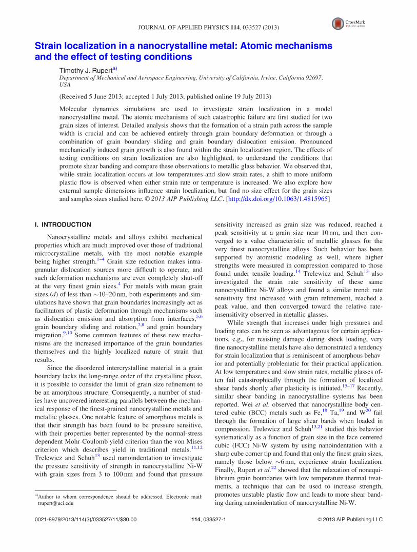
Strain localization in a nanocrystalline metal: Atomic mechanisms and theeffect of testing conditionsTimothy J. Rupert Citation: J. Appl. Phys. 114, 033527 (2013); doi: 10.1063/1.4815965 View online: http://dx.doi.org/10.1063/1.4815965 View Table of Contents: http://jap.aip.org/resource/1/JAPIAU/v114/i3 Published by the AIP Publishing LLC. Additional information on J. Appl. Phys.Journal Homepage: http://jap.aip.org/ Journal Information: http://jap.aip.org/about/about_the_journal Top downloads: http://jap.aip.org/features/most_downloaded Information for Authors: http://jap.aip.org/authors
Strain localization in a nanocrystalline metal: Atomic mechanismsand the effect of testing conditions
Timothy J. Ruperta)
Department of Mechanical and Aerospace Engineering, University of California, Irvine, California 92697,USA
(Received 5 June 2013; accepted 1 July 2013; published online 19 July 2013)
Molecular dynamics simulations are used to investigate strain localization in a model
nanocrystalline metal. The atomic mechanisms of such catastrophic failure are first studied for two
grain sizes of interest. Detailed analysis shows that the formation of a strain path across the sample
width is crucial and can be achieved entirely through grain boundary deformation or through a
combination of grain boundary sliding and grain boundary dislocation emission. Pronounced
mechanically induced grain growth is also found within the strain localization region. The effects of
testing conditions on strain localization are also highlighted, to understand the conditions that
promote shear banding and compare these observations to metallic glass behavior. We observed that,
while strain localization occurs at low temperatures and slow strain rates, a shift to more uniform
plastic flow is observed when either strain rate or temperature is increased. We also explore how
external sample dimensions influence strain localization, but find no size effect for the grain sizes
and samples sizes studied here. VC 2013 AIP Publishing LLC. [http://dx.doi.org/10.1063/1.4815965]
I. INTRODUCTION
Nanocrystalline metals and alloys exhibit mechanical
properties which are much improved over those of traditional
microcrystalline metals, with the most notable example
being higher strength.1–4 Grain size reduction makes intra-
granular dislocation sources more difficult to operate, and
such deformation mechanisms are even completely shut-off
at the very finest grain sizes.4 For metals with mean grain
sizes (d) of less than �10–20 nm, both experiments and sim-
ulations have shown that grain boundaries increasingly act as
facilitators of plastic deformation through mechanisms such
as dislocation emission and absorption from interfaces,5,6
grain boundary sliding and rotation,7,8 and grain boundary
migration.9,10 Some common features of these new mecha-
nisms are the increased importance of the grain boundaries
themselves and the highly localized nature of strain that
results.
Since the disordered intercrystalline material in a grain
boundary lacks the long-range order of the crystalline phase,
it is possible to consider the limit of grain size refinement to
be an amorphous structure. Consequently, a number of stud-
ies have uncovered interesting parallels between the mechan-
ical response of the finest-grained nanocrystalline metals and
metallic glasses. One notable feature of amorphous metals is
that their strength has been found to be pressure sensitive,
with their properties better represented by the normal-stress
dependent Mohr-Coulomb yield criterion than the von Mises
criterion which describes yield in traditional metals.11,12
Trelewicz and Schuh13 used nanoindentation to investigate
the pressure sensitivity of strength in nanocrystalline Ni-W
with grain sizes from 3 to 100 nm and found that pressure
sensitivity increased as grain size was reduced, reached a
peak sensitivity at a grain size near 10 nm, and then con-
verged to a value characteristic of metallic glasses for the
very finest nanocrystalline alloys. Such behavior has been
supported by atomistic modeling as well, where higher
strengths were measured in compression compared to those
found under tensile loading.14 Trelewicz and Schuh13 also
investigated the strain rate sensitivity of these same
nanocrystalline Ni-W alloys and found a similar trend: rate
sensitivity first increased with grain refinement, reached a
peak value, and then converged toward the relative rate-
insensitivity observed in metallic glasses.
While strength that increases under high pressures and
loading rates can be seen as advantageous for certain applica-
tions, e.g., for resisting damage during shock loading, very
fine nanocrystalline metals have also demonstrated a tendency
for strain localization that is reminiscent of amorphous behav-
ior and potentially problematic for their practical application.
At low temperatures and slow strain rates, metallic glasses of-
ten fail catastrophically through the formation of localized
shear bands shortly after plasticity is initiated.15–17 Recently,
similar shear banding in nanocrystalline systems has been
reported. Wei et al. observed that nanocrystalline body cen-
tered cubic (BCC) metals such as Fe,18 Ta,19 and W20 fail
through the formation of large shear bands when loaded in
compression. Trelewicz and Schuh13,21 studied this behavior
systematically as a function of grain size in the face centered
cubic (FCC) Ni-W system by using nanoindentation with a
sharp cube corner tip and found that only the finest grain sizes,
namely those below �6 nm, experience strain localization.
Finally, Rupert et al.22 showed that the relaxation of nonequi-
librium grain boundaries with low temperature thermal treat-
ments, a technique that can be used to increase strength,
promotes unstable plastic flow and leads to more shear band-
ing during nanoindentation of nanocrystalline Ni-W.
a)Author to whom correspondence should be addressed. Electronic mail:
0021-8979/2013/114(3)/033527/11/$30.00 VC 2013 AIP Publishing LLC114, 033527-1
JOURNAL OF APPLIED PHYSICS 114, 033527 (2013)
Molecular dynamics (MD) simulations have been an
invaluable tool for understanding strain localization physics
in metallic glasses. For example, Cao et al.23 found that the
operation of shear transformation zones (STZs) lead to a
breakdown of local icosahedral ordering in a metallic glass,
causing shear band initiation. Unfortunately, such analysis
has not been adequately extended to nanocrystalline materi-
als. Without a similar atomistic understanding of the physi-
cal mechanisms behind shear localization in nanocrystalline
metals, it is not clear how the plastic instability develops and
grows. Shimokawa et al.24 studied collective plasticity in
nanocrystalline Al with MD simulations, but restricted their
analysis to a quasi-two dimensional geometry containing co-
lumnar grains with a common out-of-plane h1 �10i orientation
(i.e., the system only contained tilt grain boundaries) and
only included 8 distinct grain orientations. Sansoz and
Dupont25 used molecular statics combined with a quasi-
continuum formulation to model nanoindentation and found
evidence of shear localization, but also restricted their dis-
cussion to a columnar grain structure. An investigation of a
three dimensional collection of nanocrystalline grains is war-
ranted in order to accurately describe the physics of the
strain localization process in a realistic nanocrystalline
system.
In this paper, we perform MD simulations of nanocrys-
talline Ni loaded in uniaxial tension. We first uncover the at-
omistic mechanisms of strain localization by studying two
wire samples with mean grain sizes of 3 and 6 nm, i.e., where
FCC metals have been observed to experience localization in
experiments. We show that localization is a process con-
trolled solely by collective grain rotation at the smallest
grain size, but dislocation activity becomes more important
as grain size is increased. We then explore the effect of test-
ing and modeling constraints such as applied strain rate, test-
ing temperature, and sample size on localization in these
materials. Our goal is to understand the conditions that pro-
mote shear banding and compare these observations to me-
tallic glass behavior. As a whole, this work serves to provide
a detailed description of the strain localization phenomenon
in a nanocrystalline metal.
II. COMPUTATIONAL METHODS
MD simulations were performed using nanocrystalline
Ni as a model system. The simulations were run with the
open-source Large-scale Atomic/Molecular Massively
Parallel Simulator (LAMMPS) code26 using an integration
time step of 2 fs and the embedded atom method (EAM)
potential from Mishin et al.,27 which accurately reproduces
mechanical properties as well as defect energies. While the
majority of prior work on nanocrystalline mechanical prop-
erties has focused on simulation cells with periodic boundary
conditions, wire geometries were used here to allow for shear
offsets at the free surfaces and a three dimensional nanocrys-
talline grain structure was simulated so that realistic localiza-
tion paths could be studied. These samples were constructed
by first forming nanocrystalline grain structures within a rec-
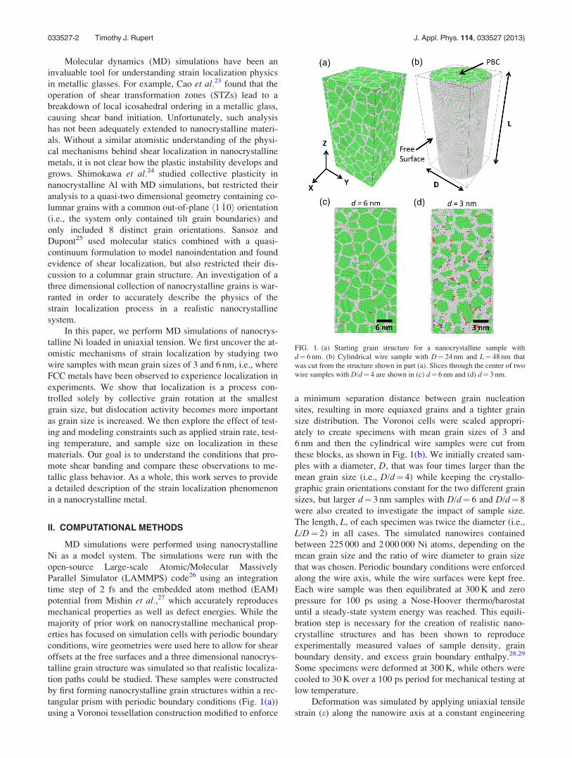
tangular prism with periodic boundary conditions (Fig. 1(a))
using a Voronoi tessellation construction modified to enforce
a minimum separation distance between grain nucleation
sites, resulting in more equiaxed grains and a tighter grain
size distribution. The Voronoi cells were scaled appropri-
ately to create specimens with mean grain sizes of 3 and
6 nm and then the cylindrical wire samples were cut from
these blocks, as shown in Fig. 1(b). We initially created sam-
ples with a diameter, D, that was four times larger than the
mean grain size (i.e., D/d¼ 4) while keeping the crystallo-
graphic grain orientations constant for the two different grain
sizes, but larger d¼ 3 nm samples with D/d¼ 6 and D/d¼ 8
were also created to investigate the impact of sample size.
The length, L, of each specimen was twice the diameter (i.e.,
L/D¼ 2) in all cases. The simulated nanowires contained
between 225 000 and 2 000 000 Ni atoms, depending on the
mean grain size and the ratio of wire diameter to grain size
that was chosen. Periodic boundary conditions were enforced
along the wire axis, while the wire surfaces were kept free.
Each wire sample was then equilibrated at 300 K and zero
pressure for 100 ps using a Nose-Hoover thermo/barostat
until a steady-state system energy was reached. This equili-
bration step is necessary for the creation of realistic nano-
crystalline structures and has been shown to reproduce
experimentally measured values of sample density, grain
boundary density, and excess grain boundary enthalpy.28,29
Some specimens were deformed at 300 K, while others were
cooled to 30 K over a 100 ps period for mechanical testing at
low temperature.
Deformation was simulated by applying uniaxial tensile
strain (e) along the nanowire axis at a constant engineering
FIG. 1. (a) Starting grain structure for a nanocrystalline sample with
d¼ 6 nm. (b) Cylindrical wire sample with D¼ 24 nm and L¼ 48 nm that
was cut from the structure shown in part (a). Slices through the center of two
wire samples with D/d¼ 4 are shown in (c) d¼ 6 nm and (d) d¼ 3 nm.
033527-2 Timothy J. Rupert J. Appl. Phys. 114, 033527 (2013)
strain rate while keeping zero stress on the other axes. Strain
rates (_eÞ between 5� 107 s�1 and 5� 109 s�1 were used and
the temperature was held constant during testing with a
Nose-Hoover thermostat. Yield strength was measured by
taking the 1% offset yield stress following prior work from
Brandstetter et al.30 and Vo et al.31 Crystal defects were
visualized with the common neighbor analysis (CNA) tech-
nique, which measures the local crystal structure around an
individual atom by quantifying the topology of bonds
between its neighboring atoms. Figs. 1(c) and 1(d) show sli-
ces through the center of nanowires with d¼ 6 nm and
d¼ 3 nm, respectively, where atoms are colored according to
CNA. In these figures, atoms in an FCC environment are
green, BCC atoms are blue, hexagonal closed packed (HCP)
atoms are red, and atoms with unknown local structure
appear white. Since Ni is an FCC metal in its crystalline
state, grain boundaries, dislocations, and other defects appear
as colors other than green. For example, a single plane of red
HCP atoms represents a twin boundary while two adjacent
HCP planes denote an intrinsic stacking fault. Comparison
of Figs. 1(c) and 1(d) shows that a larger volume fraction of
material is located in the grain boundaries of the d¼ 3 nm
sample. Atomic-level strain tensors were computed follow-
ing the work of Shimizu et al.32 and then the local von Mises
shear strain, gMises, was calculated. This quantity provided a
measurement of the local inelastic deformation experienced
by an individual atom. All atomistic visualization in this
manuscript was performed with the open-source visualiza-
tion tool OVITO.33
III. RESULTS AND DISCUSSION
A. Atomic-level observations of localizationprocesses
We first examine uniaxial tension of nanocrystalline Ni
with two different grain sizes, to identify the atomic-level
mechanisms that lead to strain localization. Since the metal-
lic glass literature suggests that shear banding occurs at low
temperatures and strain rates,11,34 we began by simulating
tensile deformation of our nanocrystalline wires at 30 K and
with an applied strain rate of 5� 107 s�1 to mimic the condi-
tions most likely to lead to highly localized plastic strain.
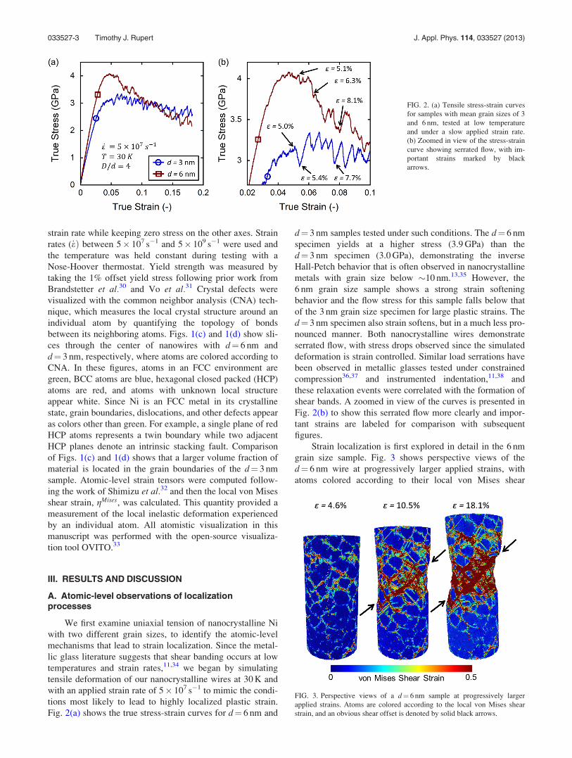
Fig. 2(a) shows the true stress-strain curves for d¼ 6 nm and
d¼ 3 nm samples tested under such conditions. The d¼ 6 nm
specimen yields at a higher stress (3.9 GPa) than the
d¼ 3 nm specimen (3.0 GPa), demonstrating the inverse
Hall-Petch behavior that is often observed in nanocrystalline
metals with grain size below �10 nm.13,35 However, the
6 nm grain size sample shows a strong strain softening
behavior and the flow stress for this sample falls below that
of the 3 nm grain size specimen for large plastic strains. The
d¼ 3 nm specimen also strain softens, but in a much less pro-
nounced manner. Both nanocrystalline wires demonstrate
serrated flow, with stress drops observed since the simulated
deformation is strain controlled. Similar load serrations have
been observed in metallic glasses tested under constrained
compression36,37 and instrumented indentation,11,38 and
these relaxation events were correlated with the formation of
shear bands. A zoomed in view of the curves is presented in
Fig. 2(b) to show this serrated flow more clearly and impor-
tant strains are labeled for comparison with subsequent
figures.
Strain localization is first explored in detail in the 6 nm
grain size sample. Fig. 3 shows perspective views of the
d¼ 6 nm wire at progressively larger applied strains, with
atoms colored according to their local von Mises shear
FIG. 2. (a) Tensile stress-strain curves
for samples with mean grain sizes of 3
and 6 nm, tested at low temperature
and under a slow applied strain rate.
(b) Zoomed in view of the stress-strain
curve showing serrated flow, with im-
portant strains marked by black
arrows.
FIG. 3. Perspective views of a d¼ 6 nm sample at progressively larger
applied strains. Atoms are colored according to the local von Mises shear
strain, and an obvious shear offset is denoted by solid black arrows.
033527-3 Timothy J. Rupert J. Appl. Phys. 114, 033527 (2013)
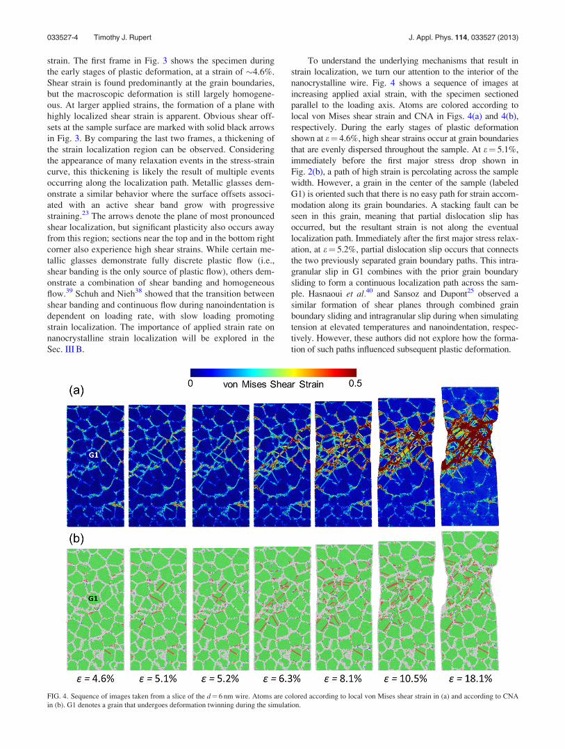
strain. The first frame in Fig. 3 shows the specimen during
the early stages of plastic deformation, at a strain of �4.6%.
Shear strain is found predominantly at the grain boundaries,
but the macroscopic deformation is still largely homogene-
ous. At larger applied strains, the formation of a plane with
highly localized shear strain is apparent. Obvious shear off-
sets at the sample surface are marked with solid black arrows
in Fig. 3. By comparing the last two frames, a thickening of
the strain localization region can be observed. Considering
the appearance of many relaxation events in the stress-strain
curve, this thickening is likely the result of multiple events
occurring along the localization path. Metallic glasses dem-
onstrate a similar behavior where the surface offsets associ-
ated with an active shear band grow with progressive
straining.23 The arrows denote the plane of most pronounced
shear localization, but significant plasticity also occurs away
from this region; sections near the top and in the bottom right
corner also experience high shear strains. While certain me-
tallic glasses demonstrate fully discrete plastic flow (i.e.,
shear banding is the only source of plastic flow), others dem-
onstrate a combination of shear banding and homogeneous
flow.39 Schuh and Nieh38 showed that the transition between
shear banding and continuous flow during nanoindentation is
dependent on loading rate, with slow loading promoting
strain localization. The importance of applied strain rate on
nanocrystalline strain localization will be explored in the
Sec. III B.
To understand the underlying mechanisms that result in
strain localization, we turn our attention to the interior of the
nanocrystalline wire. Fig. 4 shows a sequence of images at
increasing applied axial strain, with the specimen sectioned
parallel to the loading axis. Atoms are colored according to
local von Mises shear strain and CNA in Figs. 4(a) and 4(b),
respectively. During the early stages of plastic deformation
shown at e¼ 4.6%, high shear strains occur at grain boundaries
that are evenly dispersed throughout the sample. At e¼ 5.1%,
immediately before the first major stress drop shown in
Fig. 2(b), a path of high strain is percolating across the sample
width. However, a grain in the center of the sample (labeled
G1) is oriented such that there is no easy path for strain accom-
modation along its grain boundaries. A stacking fault can be
seen in this grain, meaning that partial dislocation slip has
occurred, but the resultant strain is not along the eventual
localization path. Immediately after the first major stress relax-
ation, at e¼ 5.2%, partial dislocation slip occurs that connects
the two previously separated grain boundary paths. This intra-
granular slip in G1 combines with the prior grain boundary
sliding to form a continuous localization path across the sam-
ple. Hasnaoui et al.40 and Sansoz and Dupont25 observed a
similar formation of shear planes through combined grain
boundary sliding and intragranular slip during when simulating
tension at elevated temperatures and nanoindentation, respec-
tively. However, these authors did not explore how the forma-
tion of such paths influenced subsequent plastic deformation.
FIG. 4. Sequence of images taken from a slice of the d¼ 6 nm wire. Atoms are colored according to local von Mises shear strain in (a) and according to CNA
in (b). G1 denotes a grain that undergoes deformation twinning during the simulation.
033527-4 Timothy J. Rupert J. Appl. Phys. 114, 033527 (2013)
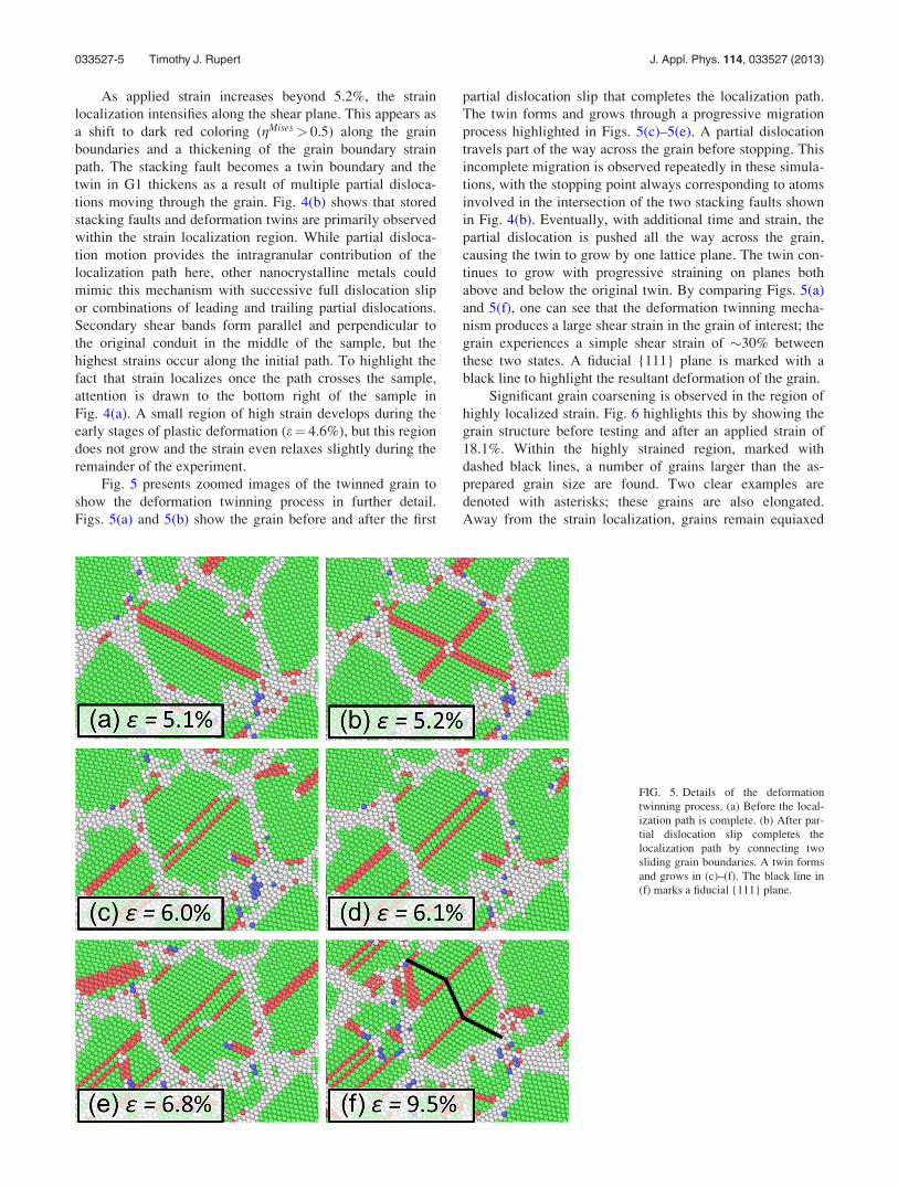
As applied strain increases beyond 5.2%, the strain
localization intensifies along the shear plane. This appears as
a shift to dark red coloring (gMises > 0.5) along the grain
boundaries and a thickening of the grain boundary strain
path. The stacking fault becomes a twin boundary and the
twin in G1 thickens as a result of multiple partial disloca-
tions moving through the grain. Fig. 4(b) shows that stored
stacking faults and deformation twins are primarily observed
within the strain localization region. While partial disloca-
tion motion provides the intragranular contribution of the
localization path here, other nanocrystalline metals could
mimic this mechanism with successive full dislocation slip
or combinations of leading and trailing partial dislocations.
Secondary shear bands form parallel and perpendicular to
the original conduit in the middle of the sample, but the
highest strains occur along the initial path. To highlight the
fact that strain localizes once the path crosses the sample,
attention is drawn to the bottom right of the sample in
Fig. 4(a). A small region of high strain develops during the
early stages of plastic deformation (e¼ 4.6%), but this region
does not grow and the strain even relaxes slightly during the
remainder of the experiment.
Fig. 5 presents zoomed images of the twinned grain to
show the deformation twinning process in further detail.
Figs. 5(a) and 5(b) show the grain before and after the first
partial dislocation slip that completes the localization path.
The twin forms and grows through a progressive migration
process highlighted in Figs. 5(c)–5(e). A partial dislocation
travels part of the way across the grain before stopping. This
incomplete migration is observed repeatedly in these simula-
tions, with the stopping point always corresponding to atoms
involved in the intersection of the two stacking faults shown
in Fig. 4(b). Eventually, with additional time and strain, the
partial dislocation is pushed all the way across the grain,
causing the twin to grow by one lattice plane. The twin con-
tinues to grow with progressive straining on planes both
above and below the original twin. By comparing Figs. 5(a)
and 5(f), one can see that the deformation twinning mecha-
nism produces a large shear strain in the grain of interest; the
grain experiences a simple shear strain of �30% between
these two states. A fiducial {111} plane is marked with a
black line to highlight the resultant deformation of the grain.
Significant grain coarsening is observed in the region of
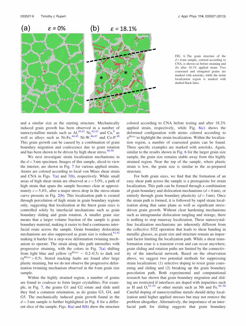
highly localized strain. Fig. 6 highlights this by showing the
grain structure before testing and after an applied strain of
18.1%. Within the highly strained region, marked with
dashed black lines, a number of grains larger than the as-
prepared grain size are found. Two clear examples are
denoted with asterisks; these grains are also elongated.
Away from the strain localization, grains remain equiaxed
FIG. 5. Details of the deformation
twinning process. (a) Before the local-
ization path is complete. (b) After par-
tial dislocation slip completes the
localization path by connecting two
sliding grain boundaries. A twin forms
and grows in (c)–(f). The black line in
(f) marks a fiducial {111} plane.
033527-5 Timothy J. Rupert J. Appl. Phys. 114, 033527 (2013)
and a similar size as the starting structure. Mechanically
induced grain growth has been observed in a number of
nanocrystalline metals such as Al,10,41 Ni,42,43 and Cu,9 as
well as alloys such as Ni-Fe,44,45 Ni-W,46,47 and Co-P.48
This grain growth can be caused by a combination of grain
boundary migration and coalescence due to grain rotation
and has been shown to be driven by high shear stress.49,50
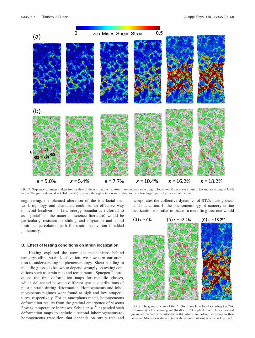
We next investigate strain localization mechanisms in
the d¼ 3 nm specimen. Images of this sample, sliced to view
the interior, are shown in Fig. 7 for various applied strains.
Atoms are colored according to local von Mises shear strain
and CNA in Figs. 7(a) and 7(b), respectively. While small
areas of high shear strain are observed at e¼ 5.0%, a path of
high strain that spans the sample becomes clear at approxi-
mately e¼ 5.4%, after a major stress drop in the stress-strain
curve presents in Fig. 2(b). This localization path is created
through percolation of high strain in grain boundary regions
only, suggesting that localization at the finest grain sizes is
controlled solely by interfacial mechanisms such as grain
boundary sliding and grain rotation. A smaller grain size
means that a larger volume fraction of the sample is grain
boundary material, making it easier to find a continuous inter-
facial route across the sample. Grain boundary dislocation
mechanisms are also suppressed as grain size is reduced,51,52
making it harder for a step-wise deformation twinning mech-
anism to operate. The strain along this path intensifies with
progressive straining, with the colors in Fig. 7(a) shifting
from light blue and yellow (gMises � 0.2–0.3) to dark red
(gMises > 0.5). Stored stacking faults are found after large
plastic straining, but we do not observe the progressive defor-
mation twinning mechanism observed in the 6 nm grain size
sample.
Within the highly strained region, a number of grains
are found to coalesce to form larger crystallites. For exam-
ple, in Fig. 7, the grains G1 and G2 rotate and slide until
they find a common orientation, as do grains G3, G4, and
G5. The mechanically induced grain growth found in the
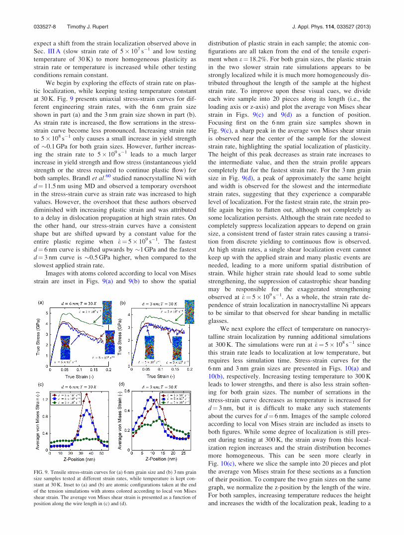
d¼ 3 nm sample is further highlighted in Fig. 8 for a differ-
ent slice of the sample. Figs. 8(a) and 8(b) show the structure
colored according to CNA before testing and after 18.2%
applied strain, respectively, while Fig. 8(c) shows the
deformed configuration with atoms colored according to
gMises to highlight the strain localization. Within the localiza-
tion region, a number of coarsened grains can be found.
Three specific examples are marked with asterisks. Again,
similar to the results shown in Fig. 6 for the larger grain size
sample, the grain size remains stable away from this highly
strained region. Near the top of the sample, where plastic
strain is low, the grain size is similar to the as-prepared
structure.
For both grain sizes, we find that the formation of an
easy shear path across the sample is a prerequisite for strain
localization. This path can be formed through a combination
of grain boundary and dislocation mechanisms (d¼ 6 nm), or
entirely through grain boundary plasticity (d¼ 3 nm). Once
the strain path is formed, it is followed by rapid strain local-
ization along that same plane as well as significant stress-
driven grain growth. Without clear hardening mechanisms
such as intragranular dislocation tangling and storage, there
is nothing to stop runaway localization. These nanocrystal-
line localization mechanisms are inherently different from
the collective STZ operation that leads to shear banding in
metallic glasses, as grain size and structure remain an impor-
tant factor limiting the localization path. While a shear trans-
formation zone is a transient event and can occur anywhere,
grain sliding and rotation paths are limited by the connectiv-
ity of the interfacial network. Based on the observation
above, we suggest two potential methods for suppressing
strain localization: (1) selective doping to resist grain coars-
ening and sliding and (2) breaking up the grain boundary
percolation path. Both experimental and computational
research has shown that grain boundary migration and slid-
ing are restricted if interfaces are doped with impurities such
as H and O,53–55 or other metals such as Nb and Fe.56–58
Careful doping of nanocrystalline metals should delay local-
ization until higher applied stresses but may not remove the
problem altogether. Alternatively, the importance of an inter-
facial path for sliding suggests that grain boundary
FIG. 6. The grain structure of the
d¼ 6 nm sample, colored according to
CNA, is shown (a) before straining and
(b) after 18.1% applied strain. Two
coarsened and elongated grains are
marked with asterisks, while the strain
localization region is marked with
dashed black lines.
033527-6 Timothy J. Rupert J. Appl. Phys. 114, 033527 (2013)
engineering, the planned alteration of the interfacial net-
work topology and character, could be an effective way
of avoid localization. Low energy boundaries (referred to
as “special” in the materials science literature) would be
particularly resistant to sliding and migration and could
limit the percolation path for strain localization if added
judiciously.
B. Effect of testing conditions on strain localization
Having explored the atomistic mechanisms behind
nanocrystalline strain localization, we now turn our atten-
tion to understanding its phenomenology. Shear banding in
metallic glasses is known to depend strongly on testing con-
ditions such as strain rate and temperature. Spaepen59 intro-
duced the first deformation maps for metallic glasses,
which delineated between different spatial distributions of
plastic strain during deformation. Homogeneous and inho-
mogeneous regimes were found at high and low tempera-
tures, respectively. For an amorphous metal, homogeneous
deformation results from the gradual emergence of viscous
flow as temperature increases. Schuh et al.34 expanded such
deformation maps to include a second inhomogeneous-to-
homogeneous transition that depends on strain rate and
incorporates the collective dynamics of STZs during shear
band nucleation. If the phenomenology of nanocrystalline
localization is similar to that of a metallic glass, one would
FIG. 8. The grain structure of the d¼ 3 nm sample, colored according to CNA,
is shown (a) before straining and (b) after 18.2% applied strain. Three coarsened
grains are marked with asterisks in (b). Atoms are colored according to their
local von Mises shear strain in (c), with the same coloring scheme as Figs. 3–7.
FIG. 7. Sequence of images taken from a slice of the d¼ 3 nm wire. Atoms are colored according to local von Mises shear strain in (a) and according to CNA
in (b). The grains denoted as G1–G5 in (b) coalesce through rotation and sliding to form two larger grains by the end of the test.
033527-7 Timothy J. Rupert J. Appl. Phys. 114, 033527 (2013)
expect a shift from the strain localization observed above in
Sec. III A (slow strain rate of 5� 107 s�1 and low testing
temperature of 30 K) to more homogeneous plasticity as
strain rate or temperature is increased while other testing
conditions remain constant.
We begin by exploring the effects of strain rate on plas-
tic localization, while keeping testing temperature constant
at 30 K. Fig. 9 presents uniaxial stress-strain curves for dif-
ferent engineering strain rates, with the 6 nm grain size
shown in part (a) and the 3 nm grain size shown in part (b).
As strain rate is increased, the flow serrations in the stress-
strain curve become less pronounced. Increasing strain rate
to 5� 108 s�1 only causes a small increase in yield strength
of �0.1 GPa for both grain sizes. However, further increas-
ing the strain rate to 5� 109 s�1 leads to a much larger
increase in yield strength and flow stress (instantaneous yield
strength or the stress required to continue plastic flow) for
both samples. Brandl et al.60 studied nanocrystalline Ni with
d¼ 11.5 nm using MD and observed a temporary overshoot
in the stress-strain curve as strain rate was increased to high
values. However, the overshoot that these authors observed
diminished with increasing plastic strain and was attributed
to a delay in dislocation propagation at high strain rates. On
the other hand, our stress-strain curves have a consistent
shape but are shifted upward by a constant value for the
entire plastic regime when _e¼ 5� 109 s�1. The fastest
d¼ 6 nm curve is shifted upwards by �1 GPa and the fastest
d¼ 3 nm curve is �0.5 GPa higher, when compared to the
slowest applied strain rate.
Images with atoms colored according to local von Mises
strain are inset in Figs. 9(a) and 9(b) to show the spatial
distribution of plastic strain in each sample; the atomic con-
figurations are all taken from the end of the tensile experi-
ment when e¼ 18.2%. For both grain sizes, the plastic strain
in the two slower strain rate simulations appears to be
strongly localized while it is much more homogeneously dis-
tributed throughout the length of the sample at the highest
strain rate. To improve upon these visual cues, we divide
each wire sample into 20 pieces along its length (i.e., the
loading axis or z-axis) and plot the average von Mises shear
strain in Figs. 9(c) and 9(d) as a function of position.
Focusing first on the 6 nm grain size samples shown in
Fig. 9(c), a sharp peak in the average von Mises shear strain
is observed near the center of the sample for the slowest
strain rate, highlighting the spatial localization of plasticity.
The height of this peak decreases as strain rate increases to
the intermediate value, and then the strain profile appears
completely flat for the fastest strain rate. For the 3 nm grain
size in Fig. 9(d), a peak of approximately the same height
and width is observed for the slowest and the intermediate
strain rates, suggesting that they experience a comparable
level of localization. For the fastest strain rate, the strain pro-
file again begins to flatten out, although not completely as
some localization persists. Although the strain rate needed to
completely suppress localization appears to depend on grain
size, a consistent trend of faster strain rates causing a transi-
tion from discrete yielding to continuous flow is observed.
At high strain rates, a single shear localization event cannot
keep up with the applied strain and many plastic events are
needed, leading to a more uniform spatial distribution of
strain. While higher strain rate should lead to some subtle
strengthening, the suppression of catastrophic shear banding
may be responsible for the exaggerated strengthening
observed at _e¼ 5� 109 s�1. As a whole, the strain rate de-
pendence of strain localization in nanocrystalline Ni appears
to be similar to that observed for shear banding in metallic
glasses.
We next explore the effect of temperature on nanocrys-
talline strain localization by running additional simulations
at 300 K. The simulations were run at _e¼ 5� 108 s�1 since
this strain rate leads to localization at low temperature, but
requires less simulation time. Stress-strain curves for the
6 nm and 3 nm grain sizes are presented in Figs. 10(a) and
10(b), respectively. Increasing testing temperature to 300 K
leads to lower strengths, and there is also less strain soften-
ing for both grain sizes. The number of serrations in the
stress-strain curve decreases as temperature is increased for
d¼ 3 nm, but it is difficult to make any such statements
about the curves for d¼ 6 nm. Images of the sample colored
according to local von Mises strain are included as insets to
both figures. While some degree of localization is still pres-
ent during testing at 300 K, the strain away from this local-
ization region increases and the strain distribution becomes
more homogeneous. This can be seen more clearly in
Fig. 10(c), where we slice the sample into 20 pieces and plot
the average von Mises strain for these sections as a function
of their position. To compare the two grain sizes on the same
graph, we normalize the z-position by the length of the wire.
For both samples, increasing temperature reduces the height
and increases the width of the localization peak, leading to a
FIG. 9. Tensile stress-strain curves for (a) 6 nm grain size and (b) 3 nm grain
size samples tested at different strain rates, while temperature is kept con-
stant at 30 K. Inset to (a) and (b) are atomic configurations taken at the end
of the tension simulations with atoms colored according to local von Mises
shear strain. The average von Mises shear strain is presented as a function of
position along the wire length in (c) and (d).
033527-8 Timothy J. Rupert J. Appl. Phys. 114, 033527 (2013)
flatter strain distribution. Again, the transition to more spa-
tially homogeneous strain at elevated temperatures mimics
metallic glass behavior. It is expected that even higher test-
ing temperatures would lead to further homogenization of
the plastic strain. However, higher temperatures would be
above our equilibration treatment temperature and could
cause thermal grain growth that would complicate a direct
comparison, so we do not perform such simulations here.
Finally, we investigate the effect of sample size on strain
localization by simulating 3 nm grain size samples with dif-
ferent wire diameters and, therefore, different numbers of
grains through the sample thickness. Experimental evidence
suggests that the mechanical behavior of nanocrystalline
pillar/wire samples can be altered if the characteristic extrin-
sic length scale of the experiment (i.e., the sample dimen-
sions) becomes comparable to the characteristic intrinsic
length scale of the material (i.e., the grain size), although
some reports suggest a softening effect with decreasing sam-
ple size61,62 while others report strengthening under similar
conditions.63 Recent MD simulations from Zhu et al. have
shown that these conflicting size scaling trends are both pos-
sible, with grain size determining which trend is observed.64
These authors found that a larger grain size of 20 nm experi-
enced softening as external dimensions were reduced while a
smaller grain size of 5 nm experienced strengthening. In
addition, we always observe mechanically induced grain
growth with our strain localization here, but such behavior
could also be influence by sample size. Using MD simula-
tions of thin film geometries, Gianola et al.55 found that
mechanically induced grain coarsening is substantially
enhanced near free surfaces and multiple authors showed
that this surface effect occurs over a length that is roughly
the order of the grain size.55,65 Our goal here is to check that
our observations are not an artifact of our relatively limited
sample size.
Additional d¼ 3 nm wires were created with diameters
of 18 and 24 nm, to complement our original sample with
D¼ 12 nm. Therefore, we tested samples with D/d ratios of
4, 6, and 8, and the largest sample had �2 000 000 atoms and
�1550 grains. Tensile simulations were run at a strain rate
of 5� 108 s�1 and a temperature of 30 K. Fig. 11(a) shows
stress-strain curves from these three samples. Yield strength
was unaffected by sample size here (3.0 GPa for all three
samples), although the number and severity of flow serra-
tions decreasing as sample size becomes larger. Fig. 11(b)
presents images where atoms are colored according to gMises
for e¼ 18.2%, and spatial strain localization is observed for
all three samples. This is confirmed by Fig. 11(c), where the
average von Mises strain is plotted against normalized z-
position and all samples show a peak in average strain. The
mechanical properties and spatial distribution of strain do
not appear to be affected by external sample size for these
simulations.
We also investigate the interior grain structure after
localization to ensure that the mechanically induced grain
growth observed in Figs. 6 and 8 was not an artifact caused
by small sample size. Figs. 12(a) and 12(b) show the largest
wire (D/d¼ 8) which has been cut down the middle and
FIG. 10. Tensile stress-strain curves
for (a) 6 nm grain size and (b) 3 nm
grain size samples tested at different
temperatures, while strain rate is kept
constant at 5� 108 s�1. Inset to (a) and
(b) are atomic configurations taken at
the end of the tension simulations with
atoms colored according to local von
Mises shear strain. The average von
Mises shear strain is presented as a
function of normalized position along
the length of the wire in (c).
FIG. 11. (a) Tensile stress-strain curves for 3 nm grain size samples with different wire diameters, while strain rate and temperature are kept constant at
5� 108 s�1 and 30 K, respectively. (b) Atomic configurations taken at the end of the tension simulations with atoms colored according to local von Mises shear
strain. The average von Mises shear strain is presented as a function of normalized position along the length of the wire in (c).
033527-9 Timothy J. Rupert J. Appl. Phys. 114, 033527 (2013)
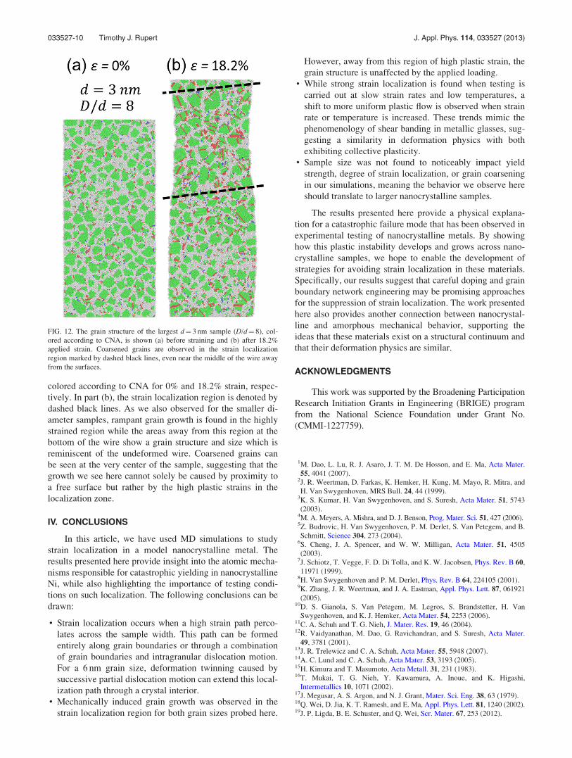
colored according to CNA for 0% and 18.2% strain, respec-
tively. In part (b), the strain localization region is denoted by
dashed black lines. As we also observed for the smaller di-
ameter samples, rampant grain growth is found in the highly
strained region while the areas away from this region at the
bottom of the wire show a grain structure and size which is
reminiscent of the undeformed wire. Coarsened grains can
be seen at the very center of the sample, suggesting that the
growth we see here cannot solely be caused by proximity to
a free surface but rather by the high plastic strains in the
localization zone.
IV. CONCLUSIONS
In this article, we have used MD simulations to study
strain localization in a model nanocrystalline metal. The
results presented here provide insight into the atomic mecha-
nisms responsible for catastrophic yielding in nanocrystalline
Ni, while also highlighting the importance of testing condi-
tions on such localization. The following conclusions can be
drawn:
• Strain localization occurs when a high strain path perco-
lates across the sample width. This path can be formed
entirely along grain boundaries or through a combination
of grain boundaries and intragranular dislocation motion.
For a 6 nm grain size, deformation twinning caused by
successive partial dislocation motion can extend this local-
ization path through a crystal interior.• Mechanically induced grain growth was observed in the
strain localization region for both grain sizes probed here.
However, away from this region of high plastic strain, the
grain structure is unaffected by the applied loading.• While strong strain localization is found when testing is
carried out at slow strain rates and low temperatures, a
shift to more uniform plastic flow is observed when strain
rate or temperature is increased. These trends mimic the
phenomenology of shear banding in metallic glasses, sug-
gesting a similarity in deformation physics with both
exhibiting collective plasticity.• Sample size was not found to noticeably impact yield
strength, degree of strain localization, or grain coarsening
in our simulations, meaning the behavior we observe here
should translate to larger nanocrystalline samples.
The results presented here provide a physical explana-
tion for a catastrophic failure mode that has been observed in
experimental testing of nanocrystalline metals. By showing
how this plastic instability develops and grows across nano-
crystalline samples, we hope to enable the development of
strategies for avoiding strain localization in these materials.
Specifically, our results suggest that careful doping and grain
boundary network engineering may be promising approaches
for the suppression of strain localization. The work presented
here also provides another connection between nanocrystal-
line and amorphous mechanical behavior, supporting the
ideas that these materials exist on a structural continuum and
that their deformation physics are similar.
ACKNOWLEDGMENTS
This work was supported by the Broadening Participation
Research Initiation Grants in Engineering (BRIGE) program
from the National Science Foundation under Grant No.
(CMMI-1227759).
1M. Dao, L. Lu, R. J. Asaro, J. T. M. De Hosson, and E. Ma, Acta Mater.
55, 4041 (2007).2J. R. Weertman, D. Farkas, K. Hemker, H. Kung, M. Mayo, R. Mitra, and
H. Van Swygenhoven, MRS Bull. 24, 44 (1999).3K. S. Kumar, H. Van Swygenhoven, and S. Suresh, Acta Mater. 51, 5743
(2003).4M. A. Meyers, A. Mishra, and D. J. Benson, Prog. Mater. Sci. 51, 427 (2006).5Z. Budrovic, H. Van Swygenhoven, P. M. Derlet, S. Van Petegem, and B.
Schmitt, Science 304, 273 (2004).6S. Cheng, J. A. Spencer, and W. W. Milligan, Acta Mater. 51, 4505
(2003).7J. Schiotz, T. Vegge, F. D. Di Tolla, and K. W. Jacobsen, Phys. Rev. B 60,
11971 (1999).8H. Van Swygenhoven and P. M. Derlet, Phys. Rev. B 64, 224105 (2001).9K. Zhang, J. R. Weertman, and J. A. Eastman, Appl. Phys. Lett. 87, 061921
(2005).10D. S. Gianola, S. Van Petegem, M. Legros, S. Brandstetter, H. Van
Swygenhoven, and K. J. Hemker, Acta Mater. 54, 2253 (2006).11C. A. Schuh and T. G. Nieh, J. Mater. Res. 19, 46 (2004).12R. Vaidyanathan, M. Dao, G. Ravichandran, and S. Suresh, Acta Mater.
49, 3781 (2001).13J. R. Trelewicz and C. A. Schuh, Acta Mater. 55, 5948 (2007).14A. C. Lund and C. A. Schuh, Acta Mater. 53, 3193 (2005).15H. Kimura and T. Masumoto, Acta Metall. 31, 231 (1983).16T. Mukai, T. G. Nieh, Y. Kawamura, A. Inoue, and K. Higashi,
Intermetallics 10, 1071 (2002).17J. Megusar, A. S. Argon, and N. J. Grant, Mater. Sci. Eng. 38, 63 (1979).18Q. Wei, D. Jia, K. T. Ramesh, and E. Ma, Appl. Phys. Lett. 81, 1240 (2002).19J. P. Ligda, B. E. Schuster, and Q. Wei, Scr. Mater. 67, 253 (2012).
FIG. 12. The grain structure of the largest d¼ 3 nm sample (D/d¼ 8), col-
ored according to CNA, is shown (a) before straining and (b) after 18.2%
applied strain. Coarsened grains are observed in the strain localization
region marked by dashed black lines, even near the middle of the wire away
from the surfaces.
033527-10 Timothy J. Rupert J. Appl. Phys. 114, 033527 (2013)
20Q. Wei, H. T. Zhang, B. E. Schuster, K. T. Ramesh, R. Z. Valiev, L. J.
Kecskes, R. J. Dowding, L. Magness, and K. Cho, Acta Mater. 54, 4079
(2006).21J. R. Trelewicz and C. A. Schuh, Appl. Phys. Lett. 93, 171916 (2008).22T. J. Rupert, J. R. Trelewicz, and C. A. Schuh, J. Mater. Res. 27, 1285
(2012).23A. J. Cao, Y. Q. Cheng, and E. Ma, Acta Mater. 57, 5146 (2009).24T. Shimokawa, T. Kinari, S. Shintaku, and A. Nakatani, Modell. Simul.
Mater. Sci. Eng. 14, S63 (2006).25F. Sansoz and V. Dupont, Mater. Sci. Eng., C 27, 1509 (2007).26S. Plimpton, J. Comput. Phys. 117, 1 (1995).27Y. Mishin, D. Farkas, M. J. Mehl, and D. A. Papaconstantopoulos, Phys.
Rev. B 59, 3393 (1999).28H. Van Swygenhoven, D. Farkas, and A. Caro, Phys. Rev. B 62, 831 (2000).29H. Van Swygenhoven, M. Spaczer, and A. Caro, Nanostruct. Mater. 12,
629 (1999).30S. Brandstetter, H. Van Swygenhoven, S. Van Petegem, B. Schmitt, R.
Maass, and P. M. Derlet, Adv. Mater. 18, 1545 (2006).31N. Q. Vo, R. S. Averback, P. Bellon, and A. Caro, Scr. Mater. 61, 76
(2009).32F. Shimizu, S. Ogata, and J. Li, Mater. Trans. 48, 2923 (2007).33A. Stukowski, Modell. Simul. Mater. Sci. Eng. 18, 015012 (2010).34C. A. Schuh, A. C. Lund, and T. G. Nieh, Acta Mater. 52, 5879
(2004).35J. Schiotz, F. D. Di Tolla, and K. W. Jacobsen, Nature 391, 561 (1998).36C. A. Pampillo and H. S. Chen, Mater. Sci. Eng. 13, 181 (1974).37Z. F. Zhang, H. Zhang, X. F. Pan, J. Das, and J. Eckert, Philos. Mag. Lett.
85, 513 (2005).38C. A. Schuh and T. G. Nieh, Acta Mater. 51, 87 (2003).39C. A. Schuh, T. C. Hufnagel, and U. Ramamurty, Acta Mater. 55, 4067
(2007).40A. Hasnaoui, H. Van Swygenhoven, and P. M. Derlet, Phys. Rev. B 66,
184112 (2002).41M. Jin, A. M. Minor, E. A. Stach, and J. W. Morris, Acta Mater. 52, 5381
(2004).42Y. B. Wang, B. Q. Li, M. L. Sui, and S. X. Mao, Appl. Phys. Lett. 92,
011903 (2008).
43D. Pan, T. G. Nieh, and M. W. Chen, Appl. Phys. Lett. 88, 161922
(2006).44G. J. Fan, Y. D. Wang, L. F. Fu, H. Choo, P. K. Liaw, Y. Ren, and N. D.
Browning, Appl. Phys. Lett. 88, 171914 (2006).45S. Cheng, Y. H. Zhao, Y. M. Wang, Y. Li, X. L. Wang, P. K. Liaw, and E.
J. Lavernia, Phys. Rev. Lett. 104, 255501 (2010).46T. J. Rupert, W. Cai, and C. A. Schuh, Wear 298–299, 120 (2013).47T. J. Rupert and C. A. Schuh, Acta Mater. 58, 4137 (2010).48G. J. Fan, L. F. Fu, D. C. Qiao, H. Choo, P. K. Liaw, and N. D. Browning,
Scr. Mater. 54, 2137 (2006).49T. J. Rupert, D. S. Gianola, Y. Gan, and K. J. Hemker, Science 326, 1686
(2009).50J. W. Cahn, Y. Mishin, and A. Suzuki, Acta Mater. 54, 4953 (2006).51N. Q. Vo, R. S. Averback, P. Bellon, S. Odunuga, and A. Caro, Phys. Rev.
B 77, 134108 (2008).52H. Van Swygenhoven, P. M. Derlet, and A. G. Froseth, Acta Mater. 54,
1975 (2006).53F. Tang, D. S. Gianola, M. P. Moody, K. J. Hemker, and J. M. Cairney,
Acta Mater. 60, 1038 (2012).54A. Elsener, O. Politano, P. M. Derlet, and H. Van Swygenhoven, Acta
Mater. 57, 1988 (2009).55D. S. Gianola, D. Farkas, M. Gamarra, and M. R. He, J. Appl. Phys. 112,
124313 (2012).56J. Schafer and K. Albe, Acta Mater. 60, 6076 (2012).57J. Schafer and K. Albe, Scr. Mater. 66, 315 (2012).58N. Q. Vo, J. Schafer, R. S. Averback, K. Albe, Y. Ashkenazy, and P.
Bellon, Scr. Mater. 65, 660 (2011).59F. Spaepen, Acta Metall. 25, 407 (1977).60C. Brandl, P. M. Derlet, and H. Van Swygenhoven, Philos. Mag. 89, 3465
(2009).61X. W. Gu, C. N. Loynachan, Z. X. Wu, Y. W. Zhang, D. J. Srolovitz, and
J. R. Greer, Nano Lett. 12, 6385 (2012).62D. C. Jang and J. R. Greer, Scr. Mater. 64, 77 (2011).63A. Rinaldi, P. Peralta, C. Friesen, and K. Sieradzki, Acta Mater. 56, 511
(2008).64Y. X. Zhu, Z. H. Li, and M. S. Huang, Scr. Mater. 68, 663 (2013).65P. M. Derlet and H. Van Swygenhoven, Philos. Mag. A 82, 1 (2002).
033527-11 Timothy J. Rupert J. Appl. Phys. 114, 033527 (2013)

![Effect of strain localization on frictional behavior of ...cjm38/papers_talks/RathbunMaroneJGR2010.pdf1. Introduction [2] The localization of strain in brittle shear zones has broad](https://img.pdfslide.us/doc/110x75/5f0f1e097e708231d442935e/effect-of-strain-localization-on-frictional-behavior-of-cjm38paperstalks.jpg)