Embed Size (px)
Citation preview
Straight boron carbide nanorods prepared from carbon nanotubes
Jinquan Wei,*a Bin Jiang,a Yanhui Li,a Cailu Xu,a Dehai Wua and Bingqing Weib
aDepartment of Mechanical Engineering, Tsinghua University, Beijing 100084, P.R. China.E-mail: [email protected]
bDepartment of Materials Science & Engineering, Rensselaer Polytechnic Institute, Troy,NY 12180, USA
Received 17th May 2002, Accepted 25th July 2002
First published as an Advance Article on the web 19th August 2002
Boron carbide nanorods were prepared on a large scale directly from the reaction of carbon nanotubes with
boron powder at 1150 uC. The bent carbon nanotubes transform into straight nanorods during the reaction.
The atomic ratio of B to C in the nanorods is very close to 4 : 1, corresponding to the compound B4C. Carbon
nanotubes act here as templates at the beginning of the formation and as a carbon source for the growth of the
boron carbide nanorods.
I. Introduction
Since the discovery of carbon nanotubes1 (CNTs), manyresearchers have paid great attention to the synthesis andproperties of similar one-dimension materials, such as BNnanotubes2–5 and B–C–N nanotubes.6 These nanotubes ornanowires are of unique structure and electronic properties.7–9
For instance, Wei et al.10 investigated electrical transportin boron-doped carbon nanotubes and found that boron-doped carbon nanotubes have lower resistivity than pureCNTs. Boron carbide is an important material with excellentmechanical and electrical properties, particularly it is veryhard.11,12 Many researchers have focused their work on thesynthesis of carbide nanowires and boron-doped CNTs usingdifferent methods. Dai et al.13 prepared carbide nanorods fromCNTs by reacting them with volatile metal or non-metalcomplexes above 1200 uC. Satishkumar et al.14 synthesizedB-doped carbon nanotubes of C35B by pyrolysis of acetylene–diborane mixtures. Han et al.15 prepared boron-doped carbonnanotubes through the partial substitution of the carbon atomson CNTs with B2O3. Although B4C and B13C2 nanorods canbe found in such samples, most of these products are B-dopednanotubes. Both Satishkumar’s and Han’s doping ratio ofboron are lower than 10% (at.%). Zhang et al.16 preparedboron carbide nanowires by using plasma-enhanced chemicalvapor deposition methods. These nanowires are of variousmorphologies and have rough walls. Han et al.15 and Maet al.17 also found boron carbide encapsulated in BN nanotubesduring their synthesis of BN nanotubes.
Due to the existence of topological pentagonal and hepta-gonal defects in the networks of rolling graphenes,18 CNTsoften occur in bent shapes or are entangled, which mightdecrease their mechanical and electrical properties. Theentangled CNTs are very difficult to disperse, resulting intheir having limited use in composites. To get straightnanotubes or nanorods is still a challenge for scientists workingin the field of one-dimensional material. In this paper, weprepare boron carbide nanorods on a large scale by usingCNTs and boron powder as raw materials. During the reactionwith boron, the bent CNTs synthesized using the chemicalvapor deposition method transform into very straight boroncarbide nanorods.
II. Experimental
The experiments were carried out in a horizontal tubularfurnace with an inner diameter of 60 mm. The CNTs used in
the experiments were prepared by chemical vapor deposition(CVD) methods19 using Ni as catalyst supported by diatomite.The as-grown carbon nanotubes were immersed in mild HFacid for 24 hours to remove the diatomite and most of themetal catalyst particles cohering on the CNTs. Boron powder(w99.5%) and CNT powder were homogeneously mixed in aB to C ratio of 4 : 1 (atomic ratio). The mixture of powderswas then placed in a ceramic boat and mounted in the middle ofthe furnace tube. The furnace was then heated to the designatedtemperature (1150 uC, for example) under the protection offlowing argon.
The obtained gray powder-like products were examined andevaluated by scanning electron microscopy (SEM), transmis-sion electron microscopy (TEM), and high-resolution trans-mission electron microscopy (HRTEM) equipped with electronenergy-loss spectroscopy (EELS). Raman spectroscopy andX-ray photoelectron spectroscopy (XPS) were also used tocharacterize the samples.
III. Results and discussion
A typical SEM image of the obtained gray powder is displayedin Fig. 1, which shows a large proportion of very straightnanorods in the sample. Although some individual bent carbonnanotubes can still be found during the SEM observation, thesample is mainly composed of straight nanorods. Some littleballs at the end of the nanorods can be frequently seen duringthe SEM observation, as the arrows show.
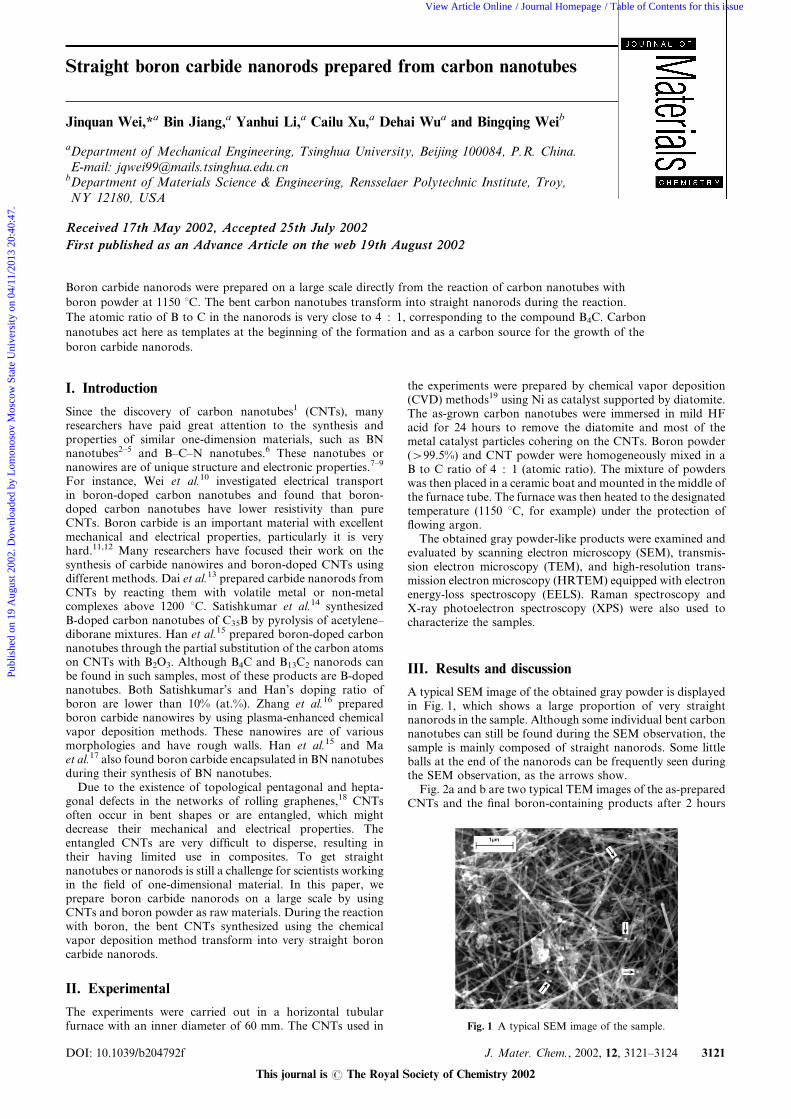
Fig. 2a and b are two typical TEM images of the as-preparedCNTs and the final boron-containing products after 2 hours
Fig. 1 A typical SEM image of the sample.
DOI: 10.1039/b204792f J. Mater. Chem., 2002, 12, 3121–3124 3121
This journal is # The Royal Society of Chemistry 2002
Publ
ishe
d on
19
Aug
ust 2
002.
Dow
nloa
ded
by L
omon
osov
Mos
cow
Sta
te U
nive
rsity
on
04/1
1/20
13 2
0:40
:47.
View Article Online / Journal Homepage / Table of Contents for this issue
reaction at 1150 uC, respectively. The as-prepared CNTs asshown in Fig. 2a are bent and tangled together. The diametersof the CNTs are about 30 nm and the lengths are up to severalmicrometers. Catalytic particles encapsulated within the CNTscan be occasionally observed during the TEM examinationdue to their survival after the acid treatment.
Abundant boron carbide nanorods can be seen in Fig. 2b.The morphologies of the nanorods, which are quite differentfrom those of the starting CNTs and those of other B-dopedCNTs and B4C nanowires,16,20,21 are surprisingly straight. Thecarbide nanorods have relatively smooth surfaces, which arequite different from the results given in ref. 14. The diametersof the nanorods are distributed between 20 nm and 60 nm,which are slightly larger than those of the as-grown CNTs,while the lengths of the nanorods are about a few micrometers,corresponding to those of the as-grown CNTs.
Some small black balls, indicated by arrow B in Fig. 2b, canoften be seen at the end of the boron carbide nanorods duringthe TEM observation. The black balls were proved to be nickel-containing particles by energy dispersive X-ray spectroscopy(EDS) equipped with HRTEM. These particles may comefrom the metal catalyst encapsulated in the CNTs, in whichthe catalyst metal was not entirely removed by HF acid. Wesuppose that these remaining nickel particles act as catalystsfor the growth of the boron carbide nanorods.
Besides boron carbide nanorods, some tubular structures,marked by arrows A, can also be seen occasionally during theTEM observation. The outer diameters of these nanotubes aresimilar to those of the as-grown CNTs, while the inner dia-meters are smaller. They are so-called B-doped carbonnanotubes.15 The atomic ratio of B to C in the B-dopednanotubes is smaller than 0.1 : 1 according to EELS mea-surements. The B-doped nanotubes can be observed more oftenwhen the reaction temperature is lower than 1100 uC, eventhough the reaction time extends to 5 hours. However, whenthe reaction temperature exceeds 1100 uC, more than 90% ofthe products are boron carbide nanorods, indicating that the
reaction temperature is a critical parameter for the formationof nanorods.
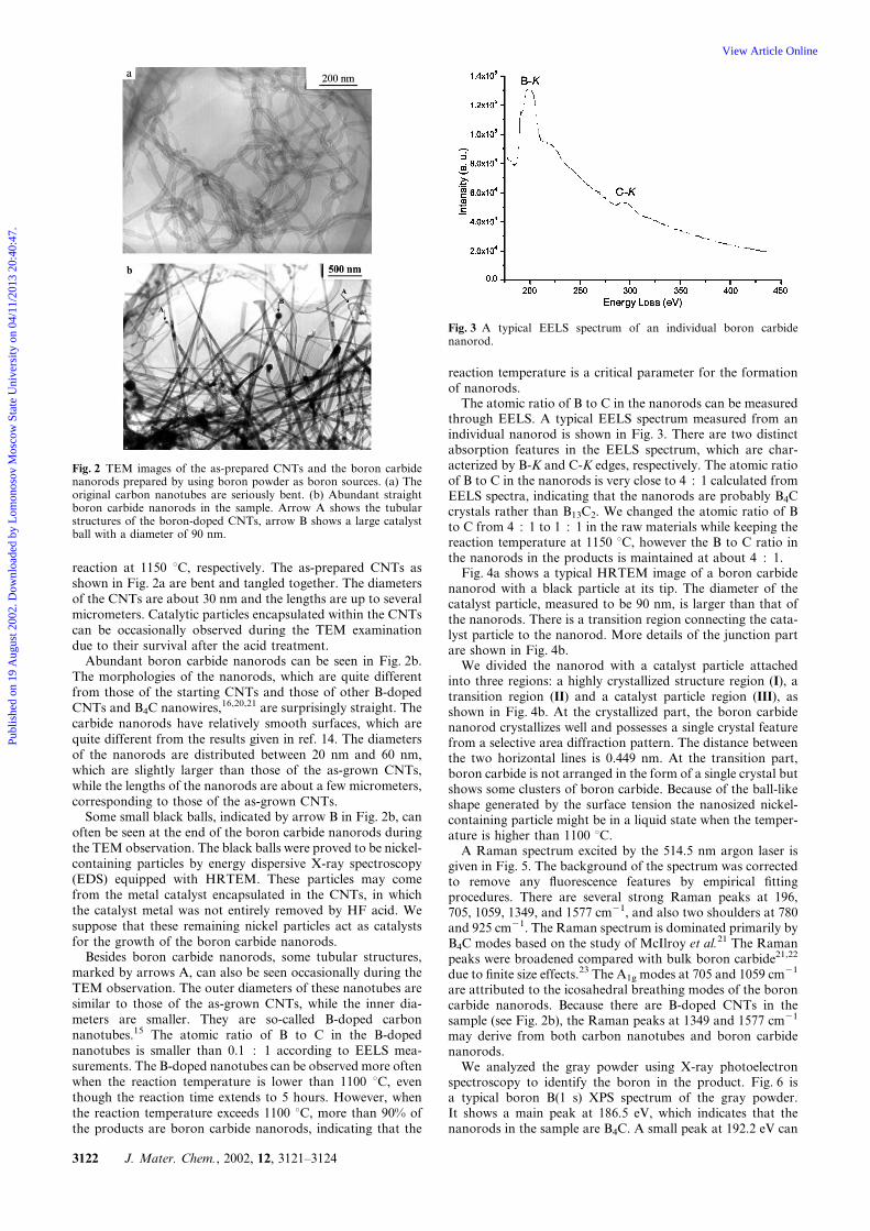
The atomic ratio of B to C in the nanorods can be measuredthrough EELS. A typical EELS spectrum measured from anindividual nanorod is shown in Fig. 3. There are two distinctabsorption features in the EELS spectrum, which are char-acterized by B-K and C-K edges, respectively. The atomic ratioof B to C in the nanorods is very close to 4 : 1 calculated fromEELS spectra, indicating that the nanorods are probably B4Ccrystals rather than B13C2. We changed the atomic ratio of Bto C from 4 : 1 to 1 : 1 in the raw materials while keeping thereaction temperature at 1150 uC, however the B to C ratio inthe nanorods in the products is maintained at about 4 : 1.
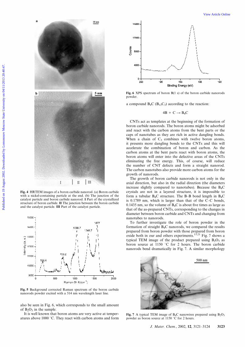
Fig. 4a shows a typical HRTEM image of a boron carbidenanorod with a black particle at its tip. The diameter of thecatalyst particle, measured to be 90 nm, is larger than that ofthe nanorods. There is a transition region connecting the cata-lyst particle to the nanorod. More details of the junction partare shown in Fig. 4b.
We divided the nanorod with a catalyst particle attachedinto three regions: a highly crystallized structure region (I), atransition region (II) and a catalyst particle region (III), asshown in Fig. 4b. At the crystallized part, the boron carbidenanorod crystallizes well and possesses a single crystal featurefrom a selective area diffraction pattern. The distance betweenthe two horizontal lines is 0.449 nm. At the transition part,boron carbide is not arranged in the form of a single crystal butshows some clusters of boron carbide. Because of the ball-likeshape generated by the surface tension the nanosized nickel-containing particle might be in a liquid state when the temper-ature is higher than 1100 uC.
A Raman spectrum excited by the 514.5 nm argon laser isgiven in Fig. 5. The background of the spectrum was correctedto remove any fluorescence features by empirical fittingprocedures. There are several strong Raman peaks at 196,705, 1059, 1349, and 1577 cm21, and also two shoulders at 780and 925 cm21. The Raman spectrum is dominated primarily byB4C modes based on the study of McIlroy et al.21 The Ramanpeaks were broadened compared with bulk boron carbide21,22
due to finite size effects.23 The A1g modes at 705 and 1059 cm21
are attributed to the icosahedral breathing modes of the boroncarbide nanorods. Because there are B-doped CNTs in thesample (see Fig. 2b), the Raman peaks at 1349 and 1577 cm21
may derive from both carbon nanotubes and boron carbidenanorods.
We analyzed the gray powder using X-ray photoelectronspectroscopy to identify the boron in the product. Fig. 6 isa typical boron B(1 s) XPS spectrum of the gray powder.It shows a main peak at 186.5 eV, which indicates that thenanorods in the sample are B4C. A small peak at 192.2 eV can
Fig. 2 TEM images of the as-prepared CNTs and the boron carbidenanorods prepared by using boron powder as boron sources. (a) Theoriginal carbon nanotubes are seriously bent. (b) Abundant straightboron carbide nanorods in the sample. Arrow A shows the tubularstructures of the boron-doped CNTs, arrow B shows a large catalystball with a diameter of 90 nm.
Fig. 3 A typical EELS spectrum of an individual boron carbidenanorod.
3122 J. Mater. Chem., 2002, 12, 3121–3124
Publ
ishe
d on
19
Aug
ust 2
002.
Dow
nloa
ded
by L
omon
osov
Mos
cow
Sta
te U
nive
rsity
on
04/1
1/20
13 2
0:40
:47.
View Article Online
also be seen in Fig. 6, which corresponds to the small amountof B2O3 in the sample.
It is well known that boron atoms are very active at temper-atures above 1000 uC. They react with carbon atoms and form
a compound B4C (B12C3) according to the reaction:
4B 1 C A B4C
CNTs act as templates at the beginning of the formation ofboron carbide nanorods. The boron atoms might be adsorbedand react with the carbon atoms from the bent parts or thecaps of nanotubes as they are rich in active dangling bonds.When a chain of C3 combines with twelve boron atoms,it presents more dangling bonds to the CNTs and this willaccelerate the combination of boron and carbon. As thecarbon atoms at the bent parts react with boron atoms, theboron atoms will enter into the defective areas of the CNTseliminating the free energy. This, of course, will reducethe number of CNT defects and form a straight nanorod.The carbon nanotubes also provide more carbon atoms for thegrowth of nanorods.
The growth of boron carbide nanorods is not only in theaxial direction, but also in the radial direction (the diametersincrease slightly compared to nanotubes). Because the B4Ccrystals are not in a layered structure, it is impossible toform a tubular B4C structure. The B–B bond length in B4Cis 0.1789 nm, which is larger than that of the C–C bonds,0.1435 nm, so the volume of B4C is about five times as large asthat of the as-prepared CNTs, corresponding to the changes indiameter between boron carbide and CNTs and changing fromnanotubes to nanorods.
To further investigate the role of boron powder in theformation of straight B4C nanorods, we compared the resultsprepared from boron powder with those prepared from boronoxide both in our and others experiments.15,21 Fig. 7 shows atypical TEM image of the product prepared using B2O3 asboron source at 1150 uC for 2 hours. The boron carbidenanorods bend dramatically in Fig. 7. A similar morphology
Fig. 4 HRTEM images of a boron carbide nanorod. (a) Boron carbidewith a nickel-containing particle at the end. (b) The junction of thecatalyst particle and boron carbide nanorod. I Part of the crystallizedstructure of boron carbide. II The junction between the boron carbideand the catalyst particle. III Part of the catalyst particle.
Fig. 5 Background corrected Raman spectrum of the boron carbidenanorods powder excited with a 514 nm wavelength laser line.
Fig. 6 XPS spectrum of boron B(1 s) of the boron carbide nanorodspowder.
Fig. 7 A typical TEM image of B4C nanowires prepared using B2O3
powder as boron source at 1150 uC for 2 hours.
J. Mater. Chem., 2002, 12, 3121–3124 3123
Publ
ishe
d on
19
Aug
ust 2
002.
Dow
nloa
ded
by L
omon
osov
Mos
cow
Sta
te U
nive
rsity
on
04/1
1/20
13 2
0:40
:47.
View Article Online
for boron-doped CNTs can be seen in ref. 15. The bent boroncarbide nanorods may result from the oxidising effect ofB2O3. When B2O3 reacts with CNTs and forms boron carbidenanorods, the oxygen atoms react with carbon atoms and formCO as well, resulting in plenty of defects in the nanorods(or B-doped nanotubes) that will change the growth directionof the nanorods.
IV. Conclusions
Straight boron carbide nanorods have been prepared success-fully on a large scale through direct reaction between CNTsand boron powder. The boron carbide nanorods straighten theCNTs and are easily dispersed. These straight B4C nanorodsmay greatly improve the mechanical properties of compositematerials and could be used in high temperature electronicdevices.
Acknowledgements
The authors gratefully acknowledge Z. Y. Cheng and X. Zhengfor performing HRTEM and EELS characterization. Theauthors also thank Professor J. Y. Yu of the ChemistryDepartment at Tsinghua University for helpful discussion ofthe Raman spectra. This work is supported financially byMOST under the State Key Project for Fundamental Research.Grant No. G20000264-04.
References
1 S. Iijima, Nature, 1991, 354, 56.2 N. G. Chopra, R. J. Luyken, K. Cherrey, V. H. Crespi,
M. L. Cohen, S. G. Louie and A. Zettl, Science, 1995, 269, 966.3 A. Loiseau, F. Willaime, N. Demoncy, G. Hug and H. Pascard,
Phys. Rev. Lett., 1996, 76, 4737.
4 D. Golberg, Y. Bando, M. Eremets, K. Takemura, K. Kurashimaand H. Yusa, Appl. Phys. Lett., 1996, 69, 2045.
5 W. Q. Han, P. Redlich, F. Ernst and M. Ruhle, Appl. Phys. Lett.,1999, 75, 1875.
6 Y. Zhang, H. Gu, K. Suenaga and S. Iijima, Chem. Phys. Lett.,1997, 279, 264.
7 D. Golberg, Y. Bando, L. Bourgeois, K. Kurashima and T. Sato,Appl. Phys. Lett., 2000, 77, 1979.
8 D. Golberg and Y. Bando, Appl. Phys. Lett., 2001, 79, 415.9 B. G. Demczyk, J. Cumings, A. Zettl and R. O. Ritchie, Appl.
Phys. Lett., 2001, 78, 2772.10 B. Q. Wei, R. Spolenak, P. Redlich, M. Ruhle and E. Arzt, Appl.
Phys. Lett., 1999, 74, 3149.11 Ali O. Sezer and J. I. Brand, Mater. Sci. Eng., B, 2001, 79, 191.12 R. Lazzari, N. Vast, J. M. Besson, S. Baroni and A. Dal Corso,
Phys. Rev. Lett., 1999, 83, 3230.13 H. J. Dai, E. W. Wong, Y. Z. Lu, S. S. Fan and C. M. Lieber,
Nature, 1995, 375, 769.14 B. C. Satishkumar, A. Govindaraj, K. R. Harikumar, J. P. Zhang,
A. K. Cheetham and C. N. R. Rao, Chem. Phys. Lett., 1999, 300,473.
15 W. Q. Han, Y. Bando, K. Kurashima and T. Sato, Chem. Phys.Lett., 1999, 299, 368.
16 D. Zhang, D. N. McIlroy, Y. Geng and M. G. Norton, J. Mater.Sci. Lett., 1999, 18, 349.
17 R. Z. Ma, Y. Bando, T. Sato and K. Kurashima, Chem. Phys.Lett., 2001, 350, 434.
18 T. W. Ebbesen and T. Takada, Carbon, 1995, 33, 973.19 M. Jose-Yacaman, M. Miki-Yoshida, L. Rendon and J. G.
Santiesteban, Appl. Phys. Lett., 1993, 62, 557.20 H. Hubert, L. A. J. Garvie, P. T. Buseck, W. T. Petuskey and
P. F. McMillan, J. Solid State Chem., 1997, 133, 356.21 D. N. McIlroy, D. Q. Zhang, R. M. Cohen, J. Wharton, Y. J. Geng,
M. G. Norton, G. De Stasio, B. Gilbert, L. Perfetti, J. H. Streiff,B. Broocks and J. L. McHale, Phys. Rev. B, 1999, 60, 4874.
22 D. R. Tallant, T. L. Aselage, A. N. Campbell and D. Emin, Phys.Rev. B, 1989, 40, 5649.
23 T. Werninghaus, J. Hahn, F. Richter and D. R. T. Zahn, Appl.Phys. Lett., 1997, 70, 958.
3124 J. Mater. Chem., 2002, 12, 3121–3124
Publ
ishe
d on
19
Aug
ust 2
002.
Dow
nloa
ded
by L
omon
osov
Mos
cow
Sta
te U
nive
rsity
on
04/1
1/20
13 2
0:40
:47.
View Article Online