Embed Size (px)
Citation preview
TABLE OF CONTENTS1. INTRODUCTION...................................................................................................................... 62. TUNER....................................................................................................................................... 7
2.1. General description of TDTC-G101D: .......................................................................... 72.2. Features of TDTC-G101D: ............................................................................................ 72.3. Pinning: .......................................................................................................................... 7
3. AUDIO AMPLIFIER STAGE WITH MAX9736(8-10WATT)................................................ 83.1. General Description........................................................................................................ 83.2. Features .......................................................................................................................... 83.3. Applications ................................................................................................................... 83.4. Absolute Ratings ............................................................................................................ 93.4.1. Electrical Characteristics............................................................................................ 93.4.2. Operating Specifications .......................................................................................... 113.5. Pinning ......................................................................................................................... 12
AUDIO AMPLIFIER STAGE WITH PT2333(2.5 WATT)............................................................ 124. POWER STAGE ...................................................................................................................... 145. MICROCONTROLLER (MSTAR)......................................................................................... 15
Genaral Description.................................................................................................................. 155.1. Features ........................................................................................................................ 15
6. MPEG-2/MPEG-4 DVB Decoder (STi7101) .......................................................................... 166.1. General Description...................................................................................................... 166.2 Features ........................................................................................................................ 186.3 Absolute Maximum Ratings......................................................................................... 21
7 DVB-T DEMODULATOR – STV0362 .................................................................................. 238.1 General Description............................................................................................................ 238.2 Features .............................................................................................................................. 258.3 Absolute Maximum Rating ................................................................................................ 268.4 Pinning ............................................................................................................................... 28
8 DVB-C DEMODULATOR – STV0297E................................................................................ 298.1 General Desription ....................................................................................................... 298.2 Features ........................................................................................................................ 298.3 Absolute Maximum Ratings......................................................................................... 308.4 Pinning ......................................................................................................................... 30
9 HY5DV281622DT-5 DDR SDRAM 128M ............................................................................ 319.1 General Description...................................................................................................... 319.2 Features ........................................................................................................................ 319.3 Absolute Maximum Ratings......................................................................................... 329.4 Pinning ......................................................................................................................... 32
10 HY5DU561622ETP-5 DDR SDRAM 256M....................................................................... 3311.1 General Description.......................................................................................................... 3311.2 Features ............................................................................................................................ 3311.3 Absolute Maximum Ratings............................................................................................. 3411.4 Pinning ............................................................................................................................. 35
11 STE100P Ethernet PHY ....................................................................................................... 3611.1 General Description...................................................................................................... 3611.2 Features ........................................................................................................................ 3611.3 Absolute Maximum Ratings......................................................................................... 3712.4 Pinning ............................................................................................................................. 38
12 SAW FILTER ...................................................................................................................... 41
12.1 IF Filter for Audio Applications – Epcos K9656M ..................................................... 4112.1.1 Standart: ................................................................................................................... 4112.1.2 Features: ................................................................................................................... 4112.1.3 Pin configuration: ..................................................................................................... 4212.1.4 Frequency response: ................................................................................................. 4212.2 IF Filter for Video Applications – Epcos K3958M...................................................... 4312.2.1 Standart: ................................................................................................................... 4312.2.2 Features: ................................................................................................................... 4312.2.3 Frequency response: ................................................................................................. 44
13 2048-Bits Serial EEPROM – 24LC02 ................................................................................. 4513.1 General Description...................................................................................................... 4513.2 Features ........................................................................................................................ 4513.3 Electrical Specifications ............................................................................................... 4613.4 Pinning ......................................................................................................................... 47
14 32K Smart Serial EEPROM – 24C32 .................................................................................. 4714.1 General Description...................................................................................................... 4714.2 Features ........................................................................................................................ 4711.3 Absolute Maximum Ratings and Electrical Characteristics......................................... 4811.4 Pinning ......................................................................................................................... 49
15 512K CMOS Serial Flash – MX25L512.............................................................................. 5015.1 General Description...................................................................................................... 5015.2 Features ........................................................................................................................ 5011.3 Absolute Maximum Ratings......................................................................................... 51
16 IC DESCRIPTIONS............................................................................................................. 5316.1 LM1117........................................................................................................................ 5316.1.1 General Description.................................................................................................. 5316.1.2 Features .................................................................................................................... 5316.1.3 Applications ............................................................................................................. 5316.1.4 Absolute Maximum Ratings..................................................................................... 5316.1.5 Pinning ..................................................................................................................... 5416.2 74HCT4053.................................................................................................................. 5416.2.1 General Description.................................................................................................. 5416.2.2 Features .................................................................................................................... 5416.2.3 Applications ............................................................................................................. 5416.2.4 Absolute Maximum Ratings..................................................................................... 5516.2.5 Pinning ..................................................................................................................... 5516.3 NUP4004M5 ................................................................................................................ 5516.3.1 General Description.................................................................................................. 5516.3.2 Features .................................................................................................................... 5616.3.3 Absolute Maximum Ratings..................................................................................... 5616.3.4 Pinning ..................................................................................................................... 5616.4 FDN336P...................................................................................................................... 5716.4.1 General Description.................................................................................................. 5716.4.2 Features .................................................................................................................... 5716.4.3 Absolute Maximum Ratings..................................................................................... 5716.4.4 Pinning ..................................................................................................................... 5716.5 TL062 -......................................................................................................................... 5816.5.1 General Description.................................................................................................. 5816.5.2 Features .................................................................................................................... 58
16.5.3 Absolute Maximum Ratings..................................................................................... 5816.5.4 Pinning ..................................................................................................................... 5916.6 PI5V330 ....................................................................................................................... 5916.6.1 General Description.................................................................................................. 5916.6.2 Features .................................................................................................................... 5916.6.3 Absolute Maximum Ratings..................................................................................... 5916.6.4 Pinning ..................................................................................................................... 6016.7 AZC099-04S ................................................................................................................ 6016.7.1 General Description.................................................................................................. 6016.7.2 Features .................................................................................................................... 6016.7.3 Absolute Maximum Ratings..................................................................................... 6116.7.4 Pinning ..................................................................................................................... 6116.8 TDA1308...................................................................................................................... 6116.8.1 General Description.................................................................................................. 6116.8.2 Features .................................................................................................................... 6116.8.3 Absolute Maximum Ratings..................................................................................... 6216.8.4 Pinning ..................................................................................................................... 6216.9 LM358D ....................................................................................................................... 6216.9.1 General Description.................................................................................................. 6216.9.2 Features .................................................................................................................... 6216.9.3 Absolute Maximum Ratings..................................................................................... 6316.9.4 Pinning ..................................................................................................................... 6316.10 74LCX244................................................................................................................ 6316.10.1 General Description.............................................................................................. 6316.10.2 Features ................................................................................................................ 6416.10.3 Absolute Maximum Ratings................................................................................. 6416.10.4 Pinning ................................................................................................................. 6516.11 74LCX245................................................................................................................ 6516.11.1 General Description.............................................................................................. 6516.11.2 Features ................................................................................................................ 6516.11.3 Absolute Maximum Ratings................................................................................. 6616.11.4 Pinning ................................................................................................................. 6616.12 FSA3157................................................................................................................... 6616.12.1 General Description.............................................................................................. 6616.12.2 Features ................................................................................................................ 6716.12.3 Absolute Maximum Ratings................................................................................. 6716.12.4 Pinning ................................................................................................................. 6716.13 TSH343 .................................................................................................................... 6816.13.1 General Description.............................................................................................. 6816.13.2 Features ................................................................................................................ 6816.13.3 Absolute Maximum Ratings................................................................................. 6816.13.4 Pinning ................................................................................................................. 6916.14 MT48LC4M16A2TG8E........................................................................................... 6916.14.1 General Description.............................................................................................. 6916.14.2 Features ................................................................................................................ 6916.14.3 Absolute Maximum Ratings................................................................................. 7016.14.4 Pinning ................................................................................................................. 7016.15 MP1583 .................................................................................................................... 7116.15.1 General Description.............................................................................................. 71
16.15.2 Features ................................................................................................................ 7116.15.3 Absolute Maximum Ratings................................................................................. 7116.15.4 Pinning ................................................................................................................. 7216.16 MP2112 .................................................................................................................... 7216.16.1 General Description.............................................................................................. 7216.16.2 Features ................................................................................................................ 7216.16.3 Absolute Maximum Ratings................................................................................. 7316.16.4 Pinning ................................................................................................................. 7316.17 MAX809LTR ........................................................................................................... 7316.17.1 General Description.............................................................................................. 7316.17.2 Features ................................................................................................................ 7316.17.3 Absolute Maximum Ratings................................................................................. 7416.17.4 Pinning ................................................................................................................. 74
17 SERVICE MENU SETTINGS............................................................................................. 7517.1 Video Setup .................................................................................................................. 7517.2 AudioSetup................................................................................................................... 7517.3 Service Scan/Tuning Setup .......................................................................................... 7717.4 Options ......................................................................................................................... 7717.5 External Source Settings .............................................................................................. 7917.6 Preset ............................................................................................................................ 8017.7 NVM Edit ..................................................................................................................... 8017.8 Programming................................................................................................................ 8017.9 Diagnostic..................................................................................................................... 8017.10 Product Info.............................................................................................................. 80
18 SOFTWARE UPDATE DESCRIPTION............................................................................. 8116.1 17MB37 Analog Part Software Update With Bootloader Procedure ......................... 8116.2 17MB37 HDCP key upload procedure. ...................................................................... 8416.3 17MB37 Digital Software Update From SCART ........................................................ 8516.4 17MB37 Digital Software Update From USB ............................................................. 90
19 BLOCK DIAGRAMS .......................................................................................................... 9119.1 General Block Diagram................................................................................................ 9119.2 Power Management...................................................................................................... 9319.3 MSTAR Block Diagram............................................................................................... 94
1. INTRODUCTION
17MB37 Main Board consists of MSTAR concept.(Up to 32”) This IC is capable of handling Video processing, Audio processing, Scaling-Display processing, 3D comb filter, OSD and text processing, 8 bit dual LVDS transmitter.TV supports PAL, SECAM, NTSC colour standards and multiple transmission standards as B/G, D/K, I/I’, and L/L’ including German and NICAM stereo.
Sound system output is supplying max. 2x8W (10%THD) for stereo 8Ω speakers. This will change according to IC thay is being used.Supported peripherals are:
1 RF input VHF I, VHF III, UHF @ 75Ohm(Common)1 Side AV (SVHS, CVBS, HP, R/L_Audio) (Common)1 SCART sockets(Common)1 YPbPr (Common)1 PC input(Optional)2 HDMI 1.3 input(2 HDMI inputs are common)1 Stereo audio input for PC(Common)1 Line out(Common)1 S/PDIF output(Common)1 Side S-Video(Optional)1 Headphone(Common)1 Common interface(Common)1 Digital USB or 1 Analog USB + 2 Digital USB(Optional)
2. TUNERA horizontal mounted and Digital Half-Nim tuner is used in the product, which covers 3 Bands(From 48MHz to 862MHz for COFDM, from 45.25MHz to 863.25MHz for CCIR CH). The tuning is available through the digitally controlled I2C bus (PLL). Below you will find info about the tuner.
2.1. General description of TDTC-G101D:The Tuner covers 3 Bands(from 48MHz to 862MHz for COFDM, from 45.25MHz to 863.25MHz for CCIR CH). Band selection and Tuning are performed digitally via the I2C bus.
2.2. Features of TDTC-G101D: Digital Half-NIM tuner for COFDM Covers 3 Bands(From 48MHz to 862MHz for COFDM, From 45.25MHz to 863.25MHz for CCIR CH) Including IF AGC with SAW Filter Bandwidth Switching (7/8 MHz) possible DC/DC Converter built in for Tuning Voltage Internal(or External) RF AGC, Antenna Power Optional
2.3. Pinning:
3. AUDIO AMPLIFIER STAGE WITH MAX9736(8-10WATT)
3.1. General DescriptionThe MAX9736A/B Class D amplifiers provide high-performance,thermally efficient amplifier solutions. The MAX9736A delivers 2 x 15W into 8Ω loads, or 1 x 30Winto a 4Ω load. The MAX9736B delivers 2 x 6W into 8Ω loads or 1 x 12W into a 4Ω load. These devices are pinfor pin compatible, allowing a single audio design to work across a broad range of platforms, simplifying design efforts, and reducing PCB inventory.Both devices operate from 8V to 28V and provide a high PSRR, eliminating the need for a regulated power supply. The MAX9736 offers up to 88% efficiency at 12V supply.Pin-selectable modulation schemes select between filterless modulation and classic PWM modulation.Filterless modulation allows the MAX9736 to pass CE EMI limits with 1m cables using only a low-cost ferrite bead and capacitor on each output. Classic PWM modulationis optimized for best audio performance when using a full LC filter.A pin-selectable stereo/mono mode allows stereo operation into 8Ω loads or mono operation into 4Ω loads. In mono mode, the right input op amp becomes available as a spare device, allowing flexibility in system design. Comprehensive click-and-pop reduction circuitry minimizes noise coming into and out of shutdown or mute.Input op amps allow the user to create summing amplifiers, lowpass or highpass filters, and select an optimal gain. The MAX9736A/B are available in 32-pin TQFN packagesand specified over the -40°C to +85°C temperature range.
3.2. FeaturesWide 8V to 28V Supply Voltage Range♦ Spread-Spectrum Modulation Enables Low EMISolution♦ Passes CE EMI Limits with Low-Cost FerriteBead/Capacitor Filter♦ Low BOM Cost, Pin-for-Pin Compatible Family♦ High 67dB PSRR at 1kHz Reduces Supply Cost♦ 88% Efficiency Eliminates Heatsink♦ Thermal and Output Current Protection♦ < 1μA Shutdown Mode♦ Mute Function♦ Space-Saving, 7mm x 7mm x 0.8mm, 32-Pin TQFNPackage
3.3. ApplicationsLCD/PDP/CRT MonitorsLCD/PDP/CRT TVsMP3 Docking StationsNotebook PCsPC SpeakersAll-in-One PCs
3.4. Absolute Ratings
3.4.1. Electrical Characteristics
3.4.2. Operating Specifications
3.5. Pinning
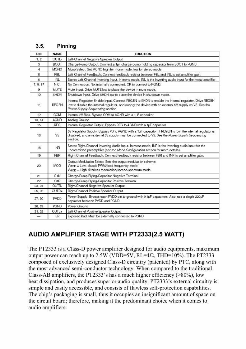
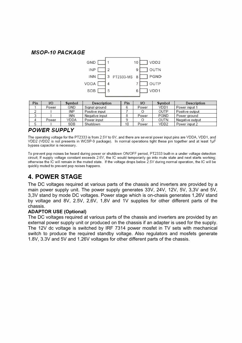
AUDIO AMPLIFIER STAGE WITH PT2333(2.5 WATT)
The PT2333 is a Class-D power amplifier designed for audio equipments, maximum output power can reach up to 2.5W (VDD=5V, RL=4Ω, THD=10%). The PT2333 composed of exclusively designed Class-D circuitry (patented) by PTC, along with the most advanced semi-conductor technology. When compared to the traditional Class-AB amplifiers, the PT2333’s has a much higher efficiency (>80%), lowheat dissipation, and produces superior audio quality. PT2333’s external circuitry is simple and easily accessible, and consists of flawless self-protection capabilities. The chip’s packaging is small, thus it occupies an insignificant amount of space on the circuit board; therefore, making it the predominant choice when it comes to audio amplifiers.
Features
CMOS technologyOperating voltage range from 2.7V up to 5.5VDifferential analog inputMaximum output power 2.5W(4Ω) @ THD=10%Output low-pass LC filter is not required.Voltage gain determinate by the external resisterContains shutdown functionPOP noises free in shutdown and power ON/OFFperiodBuilt-in short circuit protectionBuilt-in overheat protectionHigh efficiency (8Ω load >85%), low heatdissipationAvailable in MSOP 10-pin and WLCSP 9-pinminiature packages
AplicationsCellular phonePortable media playerGPSLCD monitorSmall multimedia speakersHand-free phoneLaptopOther audio applications
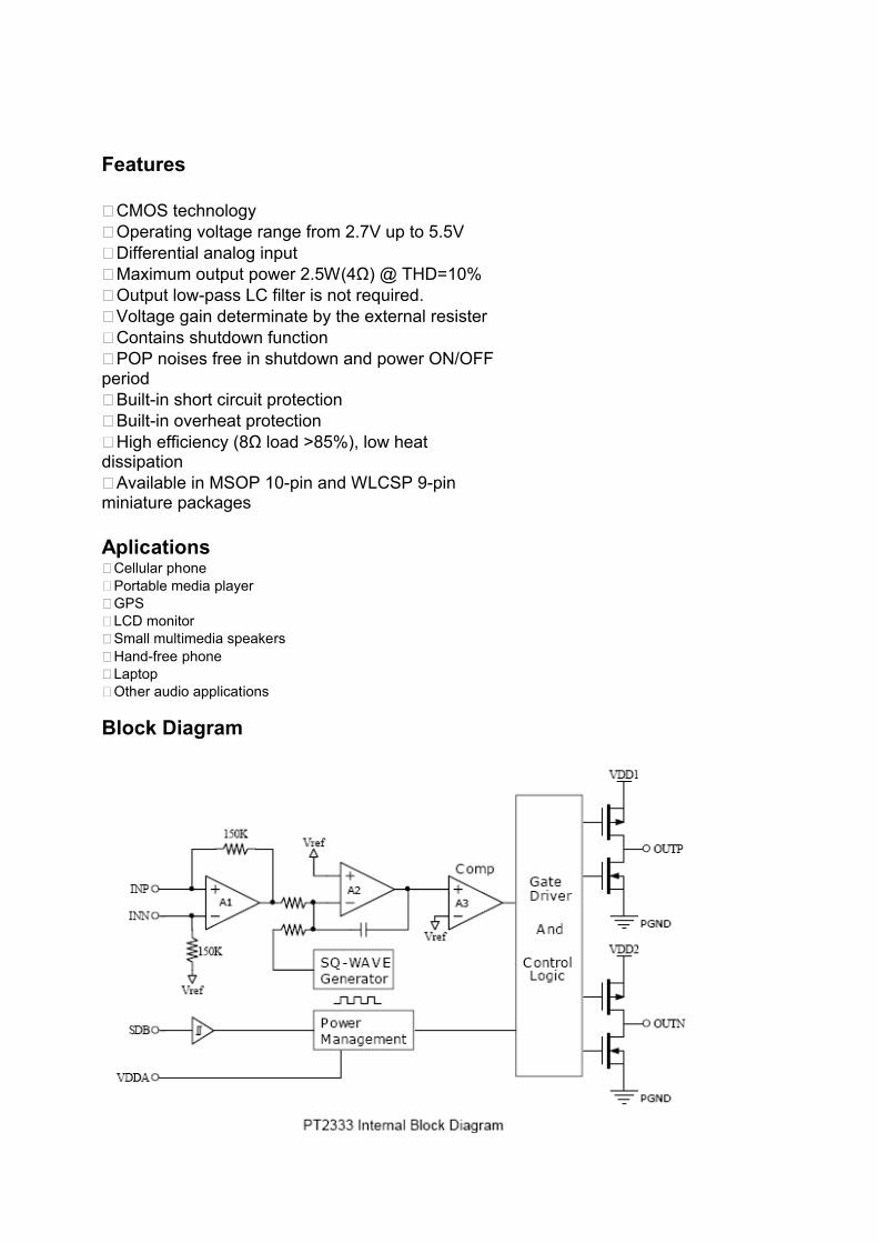
Block Diagram
4. POWER STAGEThe DC voltages required at various parts of the chassis and inverters are provided by a main power supply unit. The power supply generates 33V, 24V, 12V, 5V, 3,3V and 5V, 3,3V stand by mode DC voltages. Power stage which is on-chasis generates 1,26V stand by voltage and 8V, 2.5V, 2,6V, 1,8V and 1V supplies for other different parts of the chassis.ADAPTOR USE (Optional)The DC voltages required at various parts of the chassis and inverters are provided by an external power supply unit or produced on the chassis if an adapter is used for the supply. The 12V dc voltage is switched by IRF 7314 power mosfet in TV sets with mechanical switch to produce the required standby voltage. Also regulators and mosfets generate 1.8V, 3.3V and 5V and 1.26V voltages for other different parts of the chassis.
5. MICROCONTROLLER (MSTAR)
Genaral DescriptionThe MST6WB7GQ-3 is a high performance and fully integrated IC for multi-function LCD monitor/TV with resolutions up to full HD (1920x1080). It is configured with an integrated triple-ADC/PLL, an integrated DVI/HDCP/HDMI receiver, a multi-standard TV video and audio decoder, two video de-interlacers, two scaling engines, the MStarACE-3 color engine, an on-screen display controller, an 8-bit MCU and a built-in output panel interface. By use of external frame buffer, PIP/POP is provided for multimedia applications. Furthermore, 3-D video decoding and processing are fulfilled for high-quality TV applications. To further reduce system costs, the MST6WB7GQ-3 also integrates intelligent power management control capability for green-mode requirements and spread-spectrum support for EMI management.
5.1. Features
LCD TV controller with PIP/POP display functions Input supports up to UXGA & 1080P Panel supports up to full HD (1920x1080) TV decoder with 3-D comb filter Multi-standard TV sound demodulator and decoder 10-bit triple-ADC for TV and RGB/YPbPr 10-bit video data processing Integrated DVI/HDCP/HDMI compliant receiver High-quality dual scaling engines & dual 3-D video de-interlacers 3-D video noise reduction Full function PIP/PBP/POP MStarACE-3 picture/color processing engine Embedded On-Screen Display (OSD) controler engine Built-in MCU supports PWM & GPIO Built-in dual-link 8/10-bit LVDS transmitter 5-volt tolerant inputs Low EMI and power saving features 296-pin LQFP
NTSC/PAL/SECAM Video Decoder Supports NTSC M, NTSC-J, NTSC-4.43, PAL (B,D,G,H,M,N,I,Nc), and SECAM Automatic TV standard detection Motion adaptive 3-D comb filter for NTSC/PAL 8 configurable CVBS & Y/C S-video inputs Supports Teletext level-1.5, WSS, VPS, Closed-caption, and V-chip Macrovision detection CVBS video output
Video IF for Multi-Standard Analog TV Digital low IF architecture Stepped-gain PGA with 26 dB tuning range and 1 dB tuning resolution Maximum IF analog gain of 37dB in addition to digital gain Programmable TOP to accommodate different tuner gain to optimize noise and linearity
performance
Multi-Standard TV Sound Decoder Supports BTSC/NICAM/A2/EIA-J demodulation and decoding FM stereo & SAP demodulation L/Rx4, mono, and SIF audio inputs L/Rx3 loudspeaker and line outputs Supports sub-woofer output Built-in audio output DAC’s Audio processing for loudspeaker channel, including volume, balance, mute, tone, EQ, and
virtual stereo/surround Optional advanced surround available (Dolby1, SRS2, BBE3… etc)
Digital Audio Interface I2S digital audio input & output S/PDIF digital audio input & output HDMI audio channel processing capability Programmable delay for audio/video synchronization
Analog RGB Compliant Input Ports Three analog ports support up to UXGA Supports HDTV RGB/YPbPr/YCbCr Supports Composite Sync and SOG (Sync-on-Green) separator Automatic color calibration
DVI/HDCP/HDMI Compliant Input Port Two HDMI input ports with built-in switch Supports TMDS clock up to 225MHz @ 1080P 60Hz with 12-bit deep-color resolution Single link on-chip DVI 1.0 compliant receiver High-bandwidth Digital Content Protection(HDCP) 1.1 compliant receiver
6. MPEG-2/MPEG-4 DVB Decoder (STi7101)
6.1. General Description
The STi7101 is a new generation, high-definition IDTV / set-top box / DVD decoder chip, and provides very high performance for low-cost HD systems. STx7101 includes an H.264 video decoder for new, low bit rate applications. Based on the Omega2 (STBus) architecture, this system-on-chip is a full back-end processor for digital terrestrial, satellite, cable, DSL and IP
client high-definition set-top boxes, compliant with ATSC, DVB, DIRECTV, DCII, OpenCable and ARIB BS4 specifications. It includes all processing for DVD applications.
The STx7101 demultiplexes, decrypts and decodes HD or SD video streams with associated multi-channel audio. Video is output to two independently formatted displays: a full resolution display intended for a TV monitor, and a downsampled display intended for a VCR or DVD-R. Connection to a TV or display panel can be analog through the DACs, or digital through a copyprotected DVI/HDMI. Composite outputs are provided for connection to the VCR with Macrovision protection. Audio is output with optional PCM mixing to an S/PDIF interface, PCM interface, or through integrated stereo audio DACs. Digitized analog programs can also be input to the STx7101 for reformatting and display. The STx7101 includes a graphics rendering and display capability with a 2D graphics accelerator, three graphics planes and a cursor plane. A dual display compositor provides mixing of graphics and video with independent composition for each of the TV and VCR/DVD-R outputs. The STx7101 includes a stream merger to allow seven different transport streams from different sources to be merged and processed concurrently. Applications include DVR time-shifted viewing of a terrestrial program, while acquiring an EPG/data stream from a satellite or cable front end.
The flexible descrambling engine is compatible with required standards including DVB, DES,AES and Multi2. The STx7101 embeds a 266 MHz ST40-202 CPU for applications and device control. A dual DDR1 SDRAM memory interface is used for higher performance, to allow the video decoder the required memory bandwidth for HD H.264 and sufficient bandwidth for the CPU and the rest of the system. A second memory bus is also provided for flash memory, storing resident software, and for connection of peripherals. This bus also has a high speed synchronous mode that can be used to exchange data between two STx7101 devices. This can be used to connect a second STx7101 as a co-decoder for a dual TV STB application. A hard-disk drive (HDD) can be connected either to the serial ATA interface, or as an expansion drive through the USB 2.0 port.
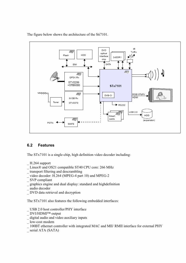
The figure below shows the architecture of the Sti7101.
6.2 Features
The STx7101 is a single-chip, high definition video decoder including:
_ H.264 support_ Linux® and OS21 compatible ST40 CPU core: 266 MHz_ transport filtering and descrambling_ video decoder: H.264 (MPEG-4 part 10) and MPEG-2_ SVP compliant_ graphics engine and dual display: standard and highdefinition_ audio decoder_ DVD data retrieval and decryption
The STx7101 also features the following embedded interfaces:
_ USB 2.0 host controller/PHY interface_ DVI/HDMI™ output_ digital audio and video auxiliary inputs_ low-cost modem_ 100BT ethernet controller with integrated MAC and MII/ RMII interface for external PHY_ serial ATA (SATA)
Processor subsystem
_ ST40 32-bit superscaler RISC CPU_ 266 MHz, 2-way set associative 16-Kbyte ICache, 32-Kbyte DCache, MMU_ 5-stage pipeline, delayed branch support_ floating point unit, matrix operation support_ debug port, interrupt controller
Transport subsystem
_ TS merger/router_ 2 serial/parallel inputs_ 1 bidirectional interface_ merging of 3 external transport streams_ transport streams from memory support_ NRSS-A module interface_ TS routing for DVB-CI and CableCARDmodules_ Programmable transport interfaces (PTIs)_ two programmable transport interfaces_ two transport stream demultiplexers: DVB, DIRECTV®, ATSC, ARIB, OpenCable, DCII_ integrated DES, AES, DVB and Multi2 descramblers_ NDS random access scrambled stream protocol (RASP) compliant_ NDS ICAM CA_ support for VGS, Passage and DVS042 residue handling
Video/graphics subsystem
_ H.264(MPEG-4 part 10) main and high profile level 4.1/MPEG-2 MP@HL video decoder_ advanced error concealment and trick mode support_ dual MPEG-2 MP@HL decode_ SD digital video input_ Displays_ one HD display multi format capable (1080I, 720P, 480P/576P, 480I/576I) analog HD output RGB or YPbPr HDMI encoded output
_ one standard-definition display analog SD output: YPbPr or YC and CVBS
_ Gamma 2D/3D graphics processor_ triple source 2D gamma blitter engine_ alpha blending and logical operations_ color space and format conversion_ fast color fill_ arbitrary resizing with high quality filters_ acceleration of direct drawing by CPU_ Gamma compositor and video processor_ 7-channel mixer for high definition output_ independent 2-channel mixer for SD output_ 3 graphic display planes_ high-quality video scaler
_ motion and detail adaptive deinterlacer_ linear resizing and format conversions_ horizontal and vertical filtering_ Copy protection_ HDMI /HDCP copy protection hardware_ SVP compliant_ Macrovision® copy protection for 480I, 480P, 576I, 576P outputs_ DTCP-IP_ AWG-based DCS analog copy protection
Audio subsystem
_ Digital audio decoder_ support for all the most popular audio standards including MPEG-1 layer I/II, MPEG-2 layer II, MPEG-2 AAC, MPEG- 4 AAC LC 2-channel/5.1 channel MPEG-4 AAC+SBR 2-channel/5.1 channel, Dolby® Digital EX, Pro Logic® II, MLP™ and DTS®_ PCM mixing with internal or external source and sample rate conversion_ 6- to 2-channel downmixing_ PCM audio input_ independent multichannel PCM output, S/PDIF output and analog output_ Stereo 24-bit audio DAC for analog output_ IEC958/IEC1937 digital audio output interface (S/PDIF)_ CSS/CPxM copy protection hardware Interfaces_ External memory interface (EMI)_ 16-bit interface supporting ROM, flash, SFlash, SRAM, peripherals_ access in 5 banks_ high speed synchronous mode for interconnecting two STx7101 devices_ External microprocessor interface (EMPI)_ 32-bit MPX satellite, target-only interface,_ synchronous operation at MPX clock speed, capable of 100 MHz,_ Dual local memory interface (LMI)_ dual interface (2 x 32-bit) for DDR1 200-MHz (DDR400) memories,
supports 128-, 256- and 512-Mbit devices_ USB 2.0 host controller/PHY interface_ Serial ATA hard-disk drive support_ record and playback with trick modes_ pause and time shifting, watch and record_ 100BT Ethernet controller, MAC and MII/RMII_ On-chip peripherals_ 4 ASCs (UARTs) with Tx and Rx FIFOS, two of which can be used in smartcard interfaces_ 2 smartcard interfaces and clock generators (improved to reduce external circuitry)_ 3 SSCs for I²C/SPI master slaves interfaces_ serial communications interface (SCIF)_ 2 PWM outputs_ teletext serializer and DMA module_ 6 banks of general purpose I/O, 3.3 V tolerant_ SiLabs line-side (DAA) interface_ modem analog front end (MAFE) interface_ infrared transmitter/receiver supporting RC5, RC6 and RECS80 codes
_ UHF remote receiver input interface_ interrupt level controller and external interrupts, 3.3 V tolerant_ low power/RTC/watchdog controller_ integrated VCXO_ DiSEqC 2.0 interface_ PWM capture/compare functions_ Flexible multi-channel DMA Services and package_ JTAG/TAP interface, ST40 toolset support, ST231 toolset support_ Package_ 35 x 35 PBGA, 580 + 100 balls (standard version)
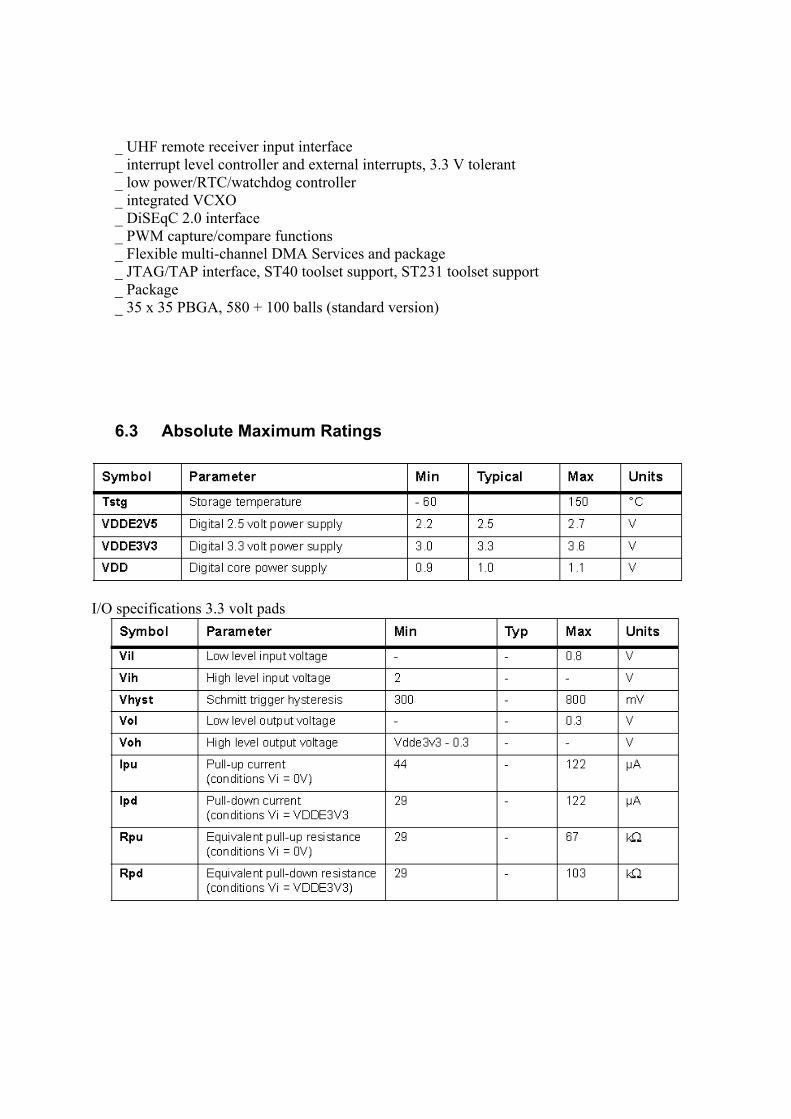
6.3 Absolute Maximum Ratings
I/O specifications 3.3 volt pads

I/O specifications 2.5 volt pads
1
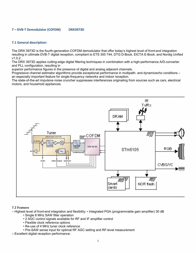
7 – DVB-T Demodulator (COFDM) DRX3973D
7.1 General description:
The DRX 3973D is the fourth-generation COFDM demodulator that offer today’s highest level of front-end integration resulting in ultimate DVB-T digital reception, compliant to ETS 300 744, DTG D-Book, EICTA E-Book, and Nordig Unified v1.0.2 .The DRX 3973D applies cutting-edge digital filtering techniques in combination with a high-performance A/D-converter and PLL configuration, resulting insuperior performance figures in the presence of digital and analog adjacent channels.Progressive channel estimator algorithms provide exceptional performance in multipath- and dynamicecho conditions –an especially important feature for single-frequency networks and indoor reception.The state-of-the-art impulsive noise cruncher suppresses interferences originating from sources such as cars, electrical motors, and household appliances.
7.2 Features– Highest level of front-end integration and flexibility: • Integrated PGA (programmable gain amplifier) 30 dB
• Single 8 MHz SAW filter operation• 2 AGC control signals available for RF and IF amplifier control• Flexible clock reference options• Re-use of 4 MHz tuner clock reference• Pre-SAW sense input for optimal RF AGC setting and RF-level measurement
– Excellent digital reception performance:
2
• Superior digital and analog adjacent channel performance (> 40dB for QEF)• Impulsive noise cruncher• Multipath and dynamic echoes
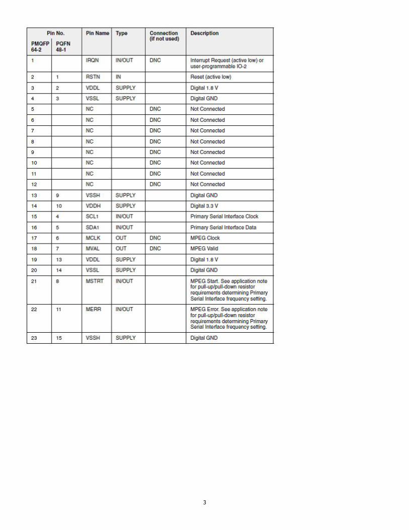
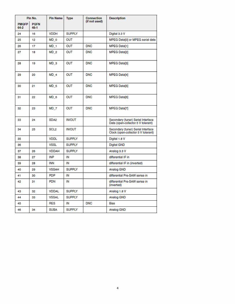
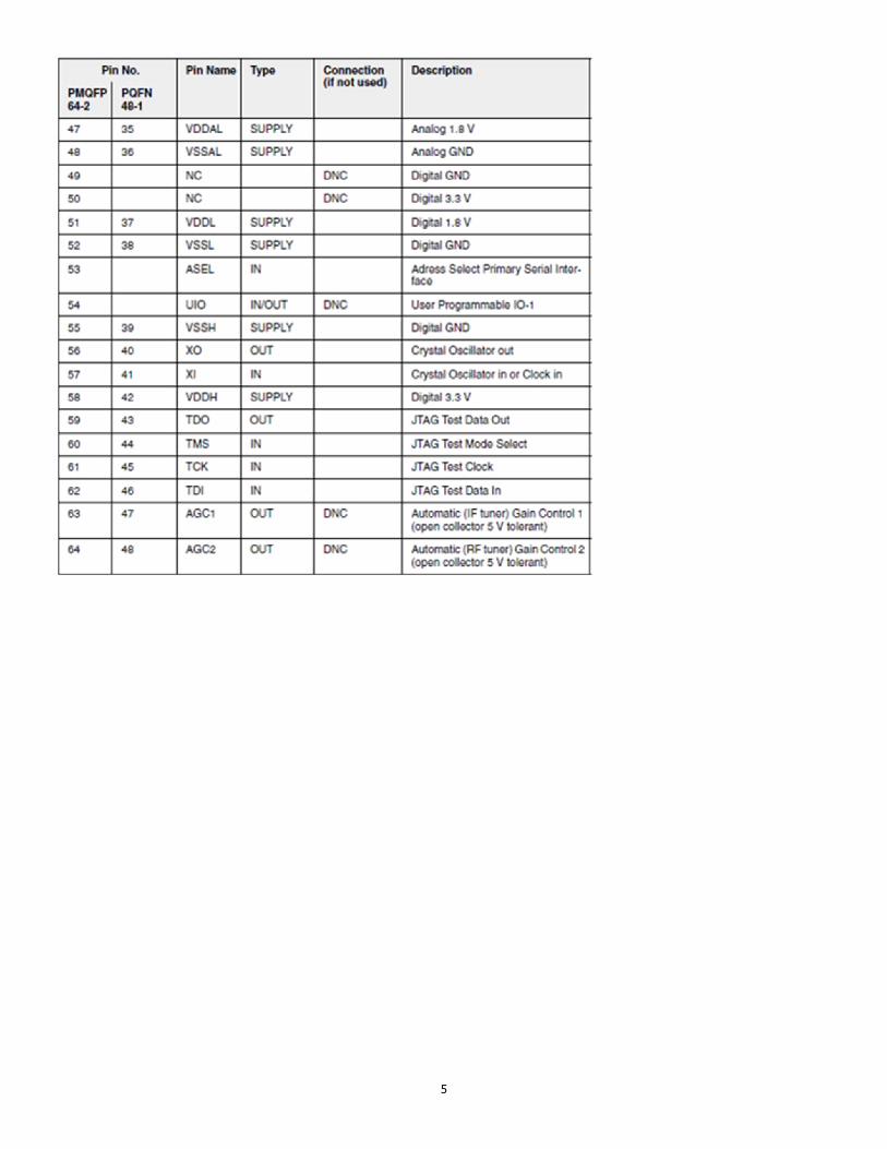
– The input IF frequency ranging up to 44 MHz ensures upward compatibility for new tuner topologies– Integrated microprocessor to perform autonomous detection and operation of all possible DVB-T modes, without interaction with the host processor– Fully automatic and fast signal acquisition: UHF and VHF band-scan in <20 seconds– Meets all international DVB-T receiver specifications: Nordig Unified, DTG, EICTA– Comfortable software drivers for integration of tuner and COFDM demodulator– Secondary serial interface for tuner control– 5 V tolerant AGC and secondary serial protocol outputs– 2 general purpose I/O pins (GPIO)– Configurable parallel or serial MPEG-TS output– PMQFP64-2 package: footprint 1010 mm (DRX 3973D)
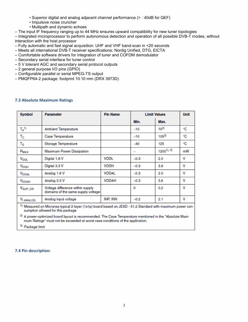
7.3 Absolute Maximum Ratings
7.4 Pin description:
3
4
5
8 DVB-C DEMODULATOR – STV0297E
8.1 General DesriptionThe STV0297E is a complete single-chip QAM (quadrature amplitude modulation)demodulation and FEC (forward error correction) solution that performs sampled IF totransport stream (MPEG-2 or MPEG-4) block processing of QAM signals. It is intended forthe digital transmission of compressed television, sound, and data services over cable. It is fully compliant with ITU-T J83 Annexes A/C or DVB-C specification bitstreams (ETS 300 429, “Digital broadcasting systems for television, sound and data services – Framingstructure, channel coding and modulation - Cable Systems”). It can handle square (16, 64, 256-QAM) and non-square (32, 128-QAM) constellations. Japanese DBS systems require a transport stream multiplex frame (TSMF) layer to carry digital signals over cable systems. When the recovered transport stream is a multiplex frame, the STV0297E post-processes it to extract a single transport stream. Automatic detection of the TSMF layer is provided. The chip integrates an analog-to-digital converter that delivers the required performance to handle up to 256-QAM signals in a direct IF sampling architecture, thus eliminating the need for external downconversion.
8.2 Features Decodes ITU-T J.83-Annexes A/C and DVB-C bit streams Processes Japanese transport stream multiplex frame (TSMF) High-performance integrated A/D converter suitable for direct IF architecture in all
QAM (quadrature amplitude modulation) modes Supports 16, 32, 64, 128 and 256 point constellations Small footprint package: (10 x 10 mm²) Very low power consumption Full digital demodulation Variable symbol rates Front derotator for better low symbol rate performance and relaxed tuner
constraints Integrated matched filtering Robust integrated adaptive pre and post equalizer On-chip FEC A/C with ability to bypass individual blocks 10 programmable GPIO Two AGC outputs suitable for delayed AGC applications (sigma-delta outputs) Integrated signal quality monitors, plus lock indicator and interrupt function mapped
to GPIO pin Improved signal acquisition System clock generated on-chip from quartz crystal Low frequency crystal operations 4, 16, 25 - 30 MHz 4 I2C addresses Easy control and monitoring via 2-wire fast I2C bus
8.3 Absolute Maximum Ratings
8.4 Pinning
9 HY5DV281622DT-5 DDR SDRAM 128M
9.1 General DescriptionThe Hynix HY5DV281622 is a 134,217,728-bit CMOS Double Data Rate(DDR) Synchronous DRAM, ideally suited for the point-to-point applications which requires high bandwidth. The Hynix 8Mx16 DDR SDRAMs offer fully synchronous operations referenced to both rising and falling edges of the clock. While all addresses and control inputs are latched on the rising edges of the CK (falling edges of the /CK), Data,Data strobes and Write data masks inputs are sampled on both rising and falling edges of it. The data paths are internally pipelined and 2-bit prefetched to achieve very high bandwidth. All input and output voltage levels are compatible with SSTL_2.
9.2 Features 3.3V for VDD and 2.5V for VDDQ power supply All inputs and outputs are compatible with SSTL_2 interface JEDEC standard 400mil 66pin TSOP-II with 0.65mm pin pitch Fully differential clock inputs (CK, /CK) operation Double data rate interface Source synchronous - data transaction aligned to bidirectional data strobe (DQS) x16 device has 2 bytewide data strobes (LDQS, UDQS) per each x8 I/O Data outputs on DQS edges when read (edged DQ) Data inputs on DQS centers
when write (centered DQ) Data(DQ) and Write masks(DM) latched on the both rising and falling edges of the
data strobe All addresses and control inputs except Data, Data strobes and Data masks
latched on the rising edges of the clock Write mask byte controls by LDM and UDM Programmable /CAS latency 3 / 4 supported Programmable Burst Length 2 / 4 / 8 with both sequential and interleave mode Internal 4 bank operations with single pulsed /RAS tRAS Lock-Out function supported Auto refresh and self refresh supported 4096 refresh cycles / 32ms Full, Half and Matched Impedance(Weak) strength driver option controlled by
EMRS
9.3 Absolute Maximum Ratings
9.4 Pinning
10 HY5DU561622ETP-5 DDR SDRAM 256M
11.1 General DescriptionThe Hynix HY5DU561622DTP is a 268,435,456-bit CMOS Double Data Rate(DDR) Synchronous DRAM, ideally suited for the point-to-point applications which requires high bandwidth. The Hynix 16Mx16 DDR SDRAMs offer fully synchronous operations referenced to both rising and falling edges of the clock. While all addresses and control inputs are latched on the rising edges of the CK (falling edges of the /CK), Data, Data strobes and Write data masks inputs are sampled on both rising and falling edges of it. The data paths are internally pipelined and 2-bit prefetched to achieve very high bandwidth. All input and output voltage levels are compatible with SSTL_2.
11.2 Features
• 2.5V +/-5% VDD and VDDQ power supplysupports 200 / 166MHz• All inputs and outputs are compatible with SSTL_2 interface• JEDEC standard 400mil 66pin TSOP-II with 0.65mm pin pitch• Fully differential clock inputs (CK, /CK) operation• Double data rate interface• Source synchronous - data transaction aligned to bidirectional data strobe (DQS)• x16 device has 2 bytewide data strobes (LDQS,UDQS) per each x8 I/O• Data outputs on DQS edges when read (edged DQ)Data inputs on DQS centers when write (centered DQ)• Data(DQ) and Write masks(DM) latched on the both rising and falling edges of the data strobe• All addresses and control inputs except Data, Data strobes and Data masks latched on the rising edgesof the clock• Write mask byte controls by LDM and UDM • Programmable /CAS latency 3 / 4 supported• Programmable Burst Length 2 / 4 / 8 with both sequential and interleave mode• Internal 4 bank operations with single pulsed /RAS• tRAS Lock-Out function supported• Auto refresh and self refresh supported• 8192 refresh cycles / 64ms• Full, Half and Matched Impedance(Weak) strength driver option controlled by EMRS
11.3 Absolute Maximum Ratings
11.4 Pinning
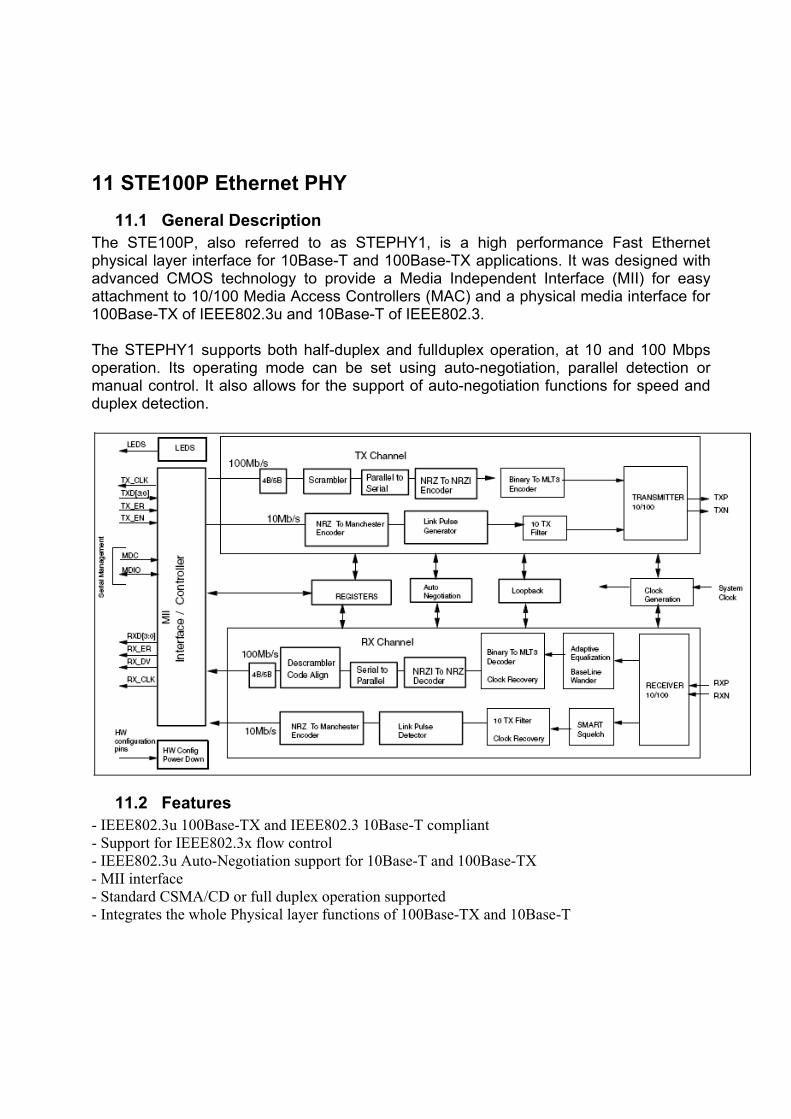
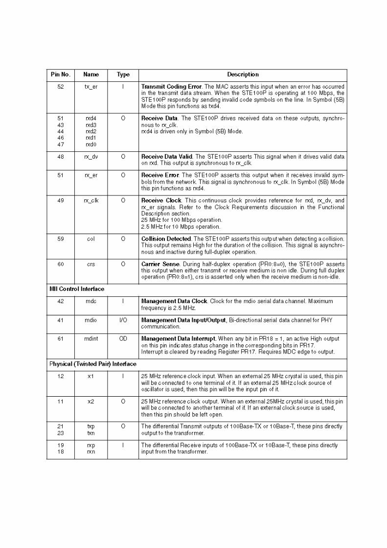
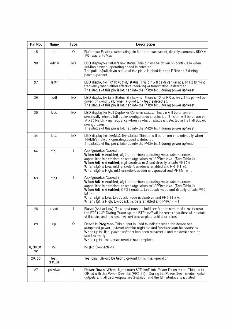
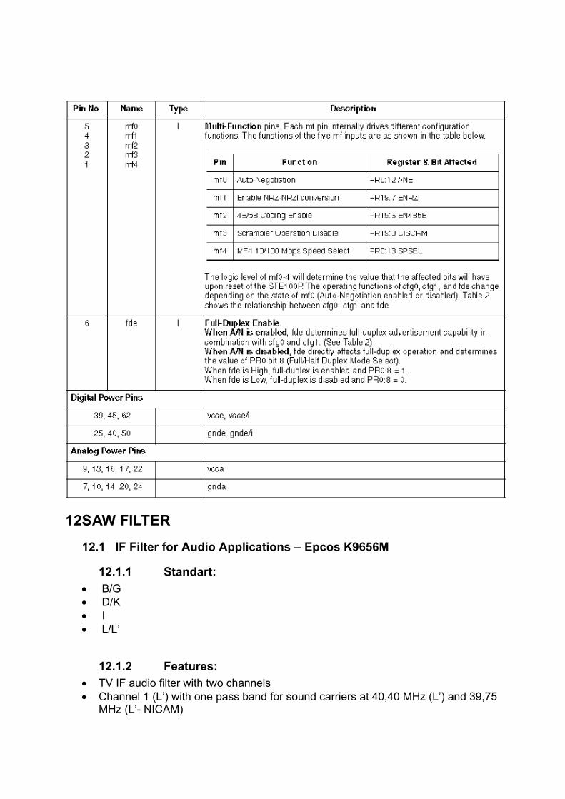
11 STE100P Ethernet PHY
11.1 General DescriptionThe STE100P, also referred to as STEPHY1, is a high performance Fast Ethernet physical layer interface for 10Base-T and 100Base-TX applications. It was designed with advanced CMOS technology to provide a Media Independent Interface (MII) for easy attachment to 10/100 Media Access Controllers (MAC) and a physical media interface for 100Base-TX of IEEE802.3u and 10Base-T of IEEE802.3.
The STEPHY1 supports both half-duplex and fullduplex operation, at 10 and 100 Mbps operation. Its operating mode can be set using auto-negotiation, parallel detection or manual control. It also allows for the support of auto-negotiation functions for speed and duplex detection.
11.2 Features- IEEE802.3u 100Base-TX and IEEE802.3 10Base-T compliant- Support for IEEE802.3x flow control- IEEE802.3u Auto-Negotiation support for 10Base-T and 100Base-TX- MII interface- Standard CSMA/CD or full duplex operation supported- Integrates the whole Physical layer functions of 100Base-TX and 10Base-T
- Provides Full-duplex operation on both 100Mbps and 10Mbps modes- Provides Auto-negotiation(NWAY) function of full/half duplex operation for both 10 and 100 Mbps- Provides MLT-3 transceiver with DC restoration for Base-line wander compensation- Provides transmit wave-shaper, receive filters, and adaptive equalizer- Provides loop-back modes for diagnostic- Builds in Stream Cipher Scrambler/ De-scrambler and 4B/5B encoder/decoder- Supports external transmit transformer with turn ratio 1:1- Supports external receive transformer with turn ratio 1:1- Standard 64-pin QFP package pinout
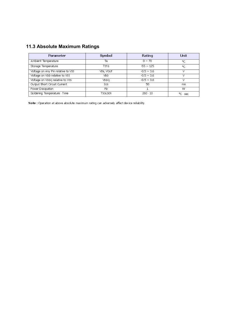
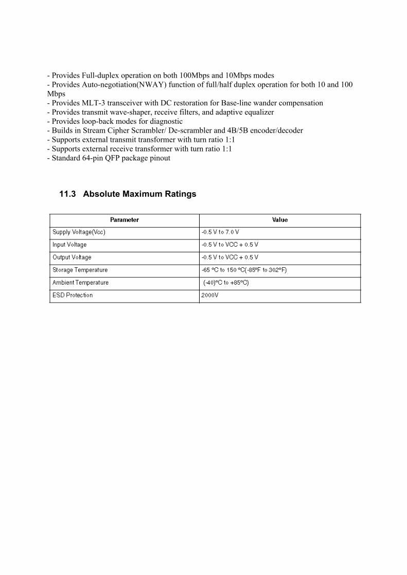
11.3 Absolute Maximum Ratings
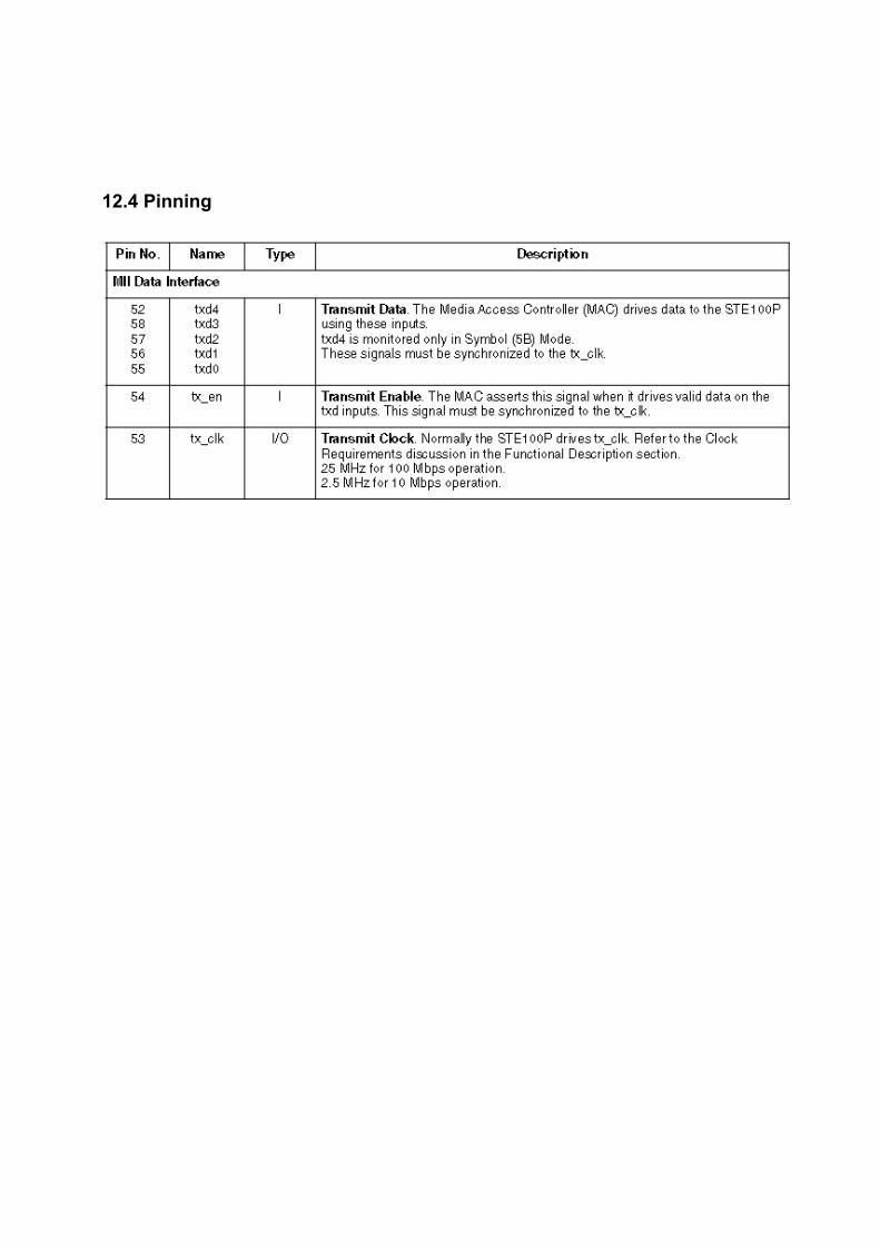
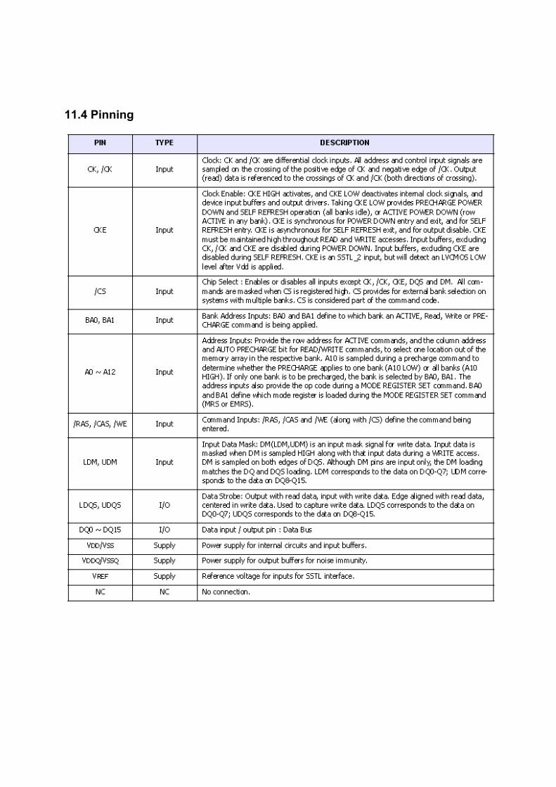
12.4 Pinning
12SAW FILTER
12.1 IF Filter for Audio Applications – Epcos K9656M
12.1.1 Standart: B/G D/K I L/L’
12.1.2 Features: TV IF audio filter with two channels Channel 1 (L’) with one pass band for sound carriers at 40,40 MHz (L’) and 39,75
MHz (L’- NICAM)
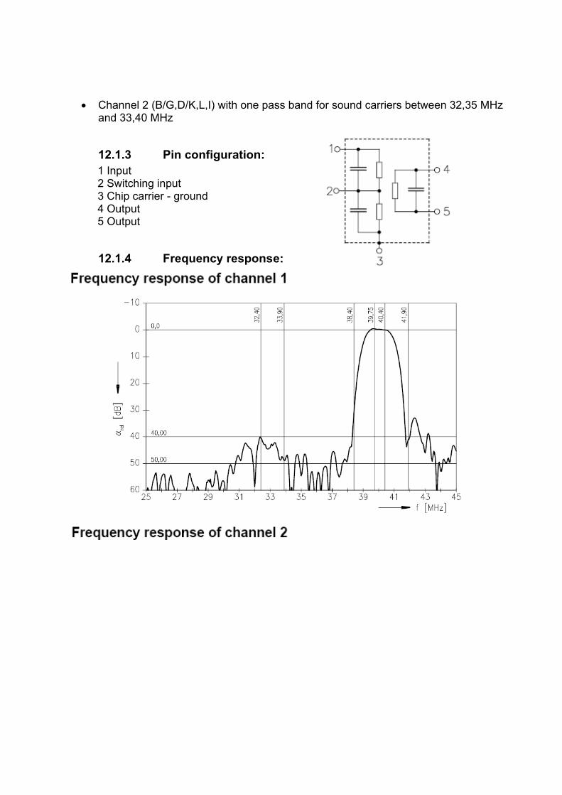
Channel 2 (B/G,D/K,L,I) with one pass band for sound carriers between 32,35 MHz and 33,40 MHz
12.1.3 Pin configuration: 1 Input2 Switching input3 Chip carrier - ground4 Output5 Output
12.1.4 Frequency response:
12.2 IF Filter for Video Applications – Epcos K3958M
12.2.1 Standart: B/G D/K I L/L’
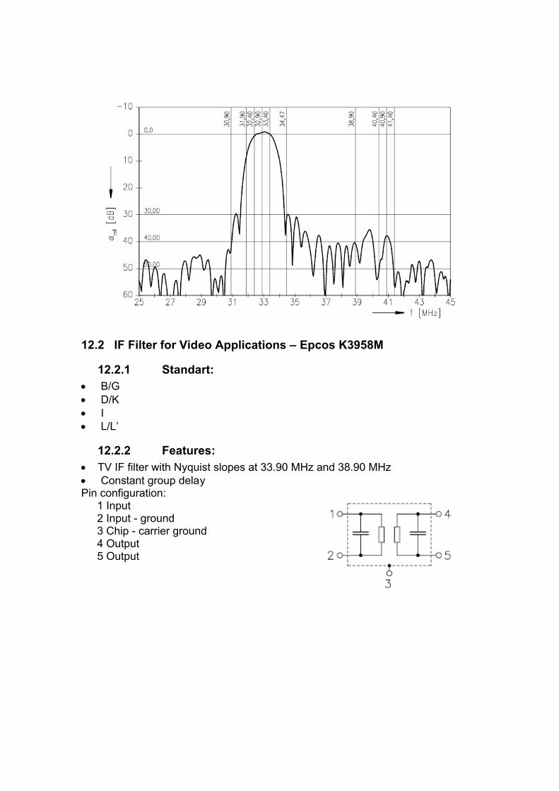
12.2.2 Features: TV IF filter with Nyquist slopes at 33.90 MHz and 38.90 MHz Constant group delayPin configuration:
1 Input2 Input - ground3 Chip - carrier ground4 Output5 Output
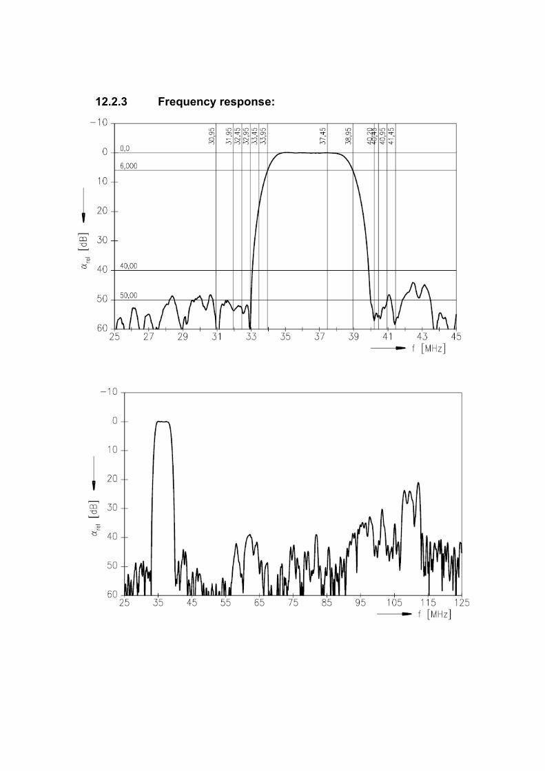
12.2.3 Frequency response:
132048-Bits Serial EEPROM – 24LC02
13.1 General DescriptionThe 24LC01/02 is a 1K/2K-bit serial read/write non-volatile memory device using the CMOS floating gate process. Its 1024/2048 bits of memory are organized into 128/256words and each word is 8 bits. The device is optimized for use in many industrial and commercial applications where low power and low voltage operation are essential. Up to eight HT24LC01/02 devices may be connected to the same two-wire bus. The HT24LC01/02 is guaranteed for 1M erase/write cycles and 40-year data retention.
13.2 Features Operating voltage: 2.4V~5.5V Low power consumption Operation: 5mA max. Standby: 5mA max. Internal organization 1K (HT24LC01):128´8 2K (HT24LC02): 256´8 2-wire serial interface Write cycle time: 5ms max. Automatic erase-before-write operation Partial page write allowed 8-byte Page write modes Write operation with built-in timer Hardware controlled write protection 40-year data retention 106 erase/write cycles per word 8-pin DIP/SOP package 8-pin TSSOP (HT24LC02 only) Commerical temperature range (0°C to +70°C)
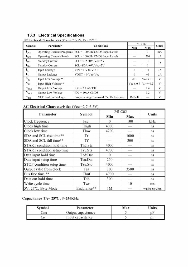
13.3 Electrical Specifications
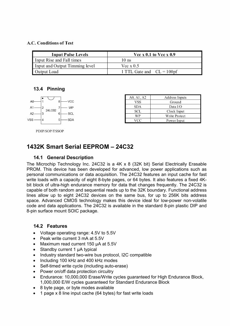
13.4 Pinning
1432K Smart Serial EEPROM – 24C32
14.1 General DescriptionThe Microchip Technology Inc. 24C32 is a 4K x 8 (32K bit) Serial Electrically Erasable PROM. This device has been developed for advanced, low power applications such as personal communications or data acquisition. The 24C32 features an input cache for fast write loads with a capacity of eight 8-byte pages, or 64 bytes. It also features a fixed 4K-bit block of ultra-high endurance memory for data that changes frequently. The 24C32 is capable of both random and sequential reads up to the 32K boundary. Functional address lines allow up to eight 24C32 devices on the same bus, for up to 256K bits address space. Advanced CMOS technology makes this device ideal for low-power non-volatilecode and data applications. The 24C32 is available in the standard 8-pin plastic DIP and 8-pin surface mount SOIC package.
14.2 Features Voltage operating range: 4.5V to 5.5V Peak write current 3 mA at 5.5V Maximum read current 150 µA at 5.5V Standby current 1 µA typical Industry standard two-wire bus protocol, I2C compatible Including 100 kHz and 400 kHz modes Self-timed write cycle (including auto-erase) Power on/off data protection circuitry Endurance: 10,000,000 Erase/Write cycles guaranteed for High Endurance Block,
1,000,000 E/W cycles guaranteed for Standard Endurance Block 8 byte page, or byte modes available 1 page x 8 line input cache (64 bytes) for fast write loads
Schmitt trigger, filtered inputs for noise suppression Output slope control to eliminate ground bounce 2 ms typical write cycle time, byte or page Up to 8 chips may be connected to the same bus for up to 256K bits total memory Electrostatic discharge protection > 4000V Data retention > 200 years 8-pin PDIP/SOIC packages Temperature ranges: Commercial (C): 0°C to +70°C, Industrial (I): -40°C to +85°C
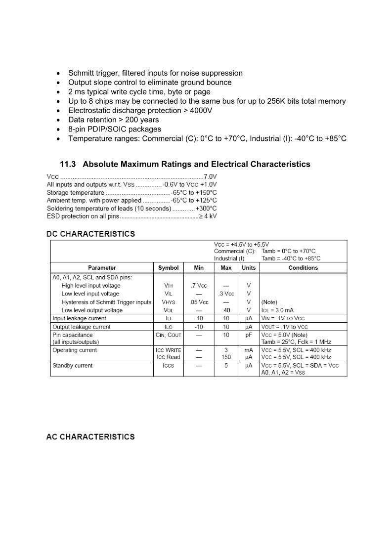
11.3 Absolute Maximum Ratings and Electrical Characteristics
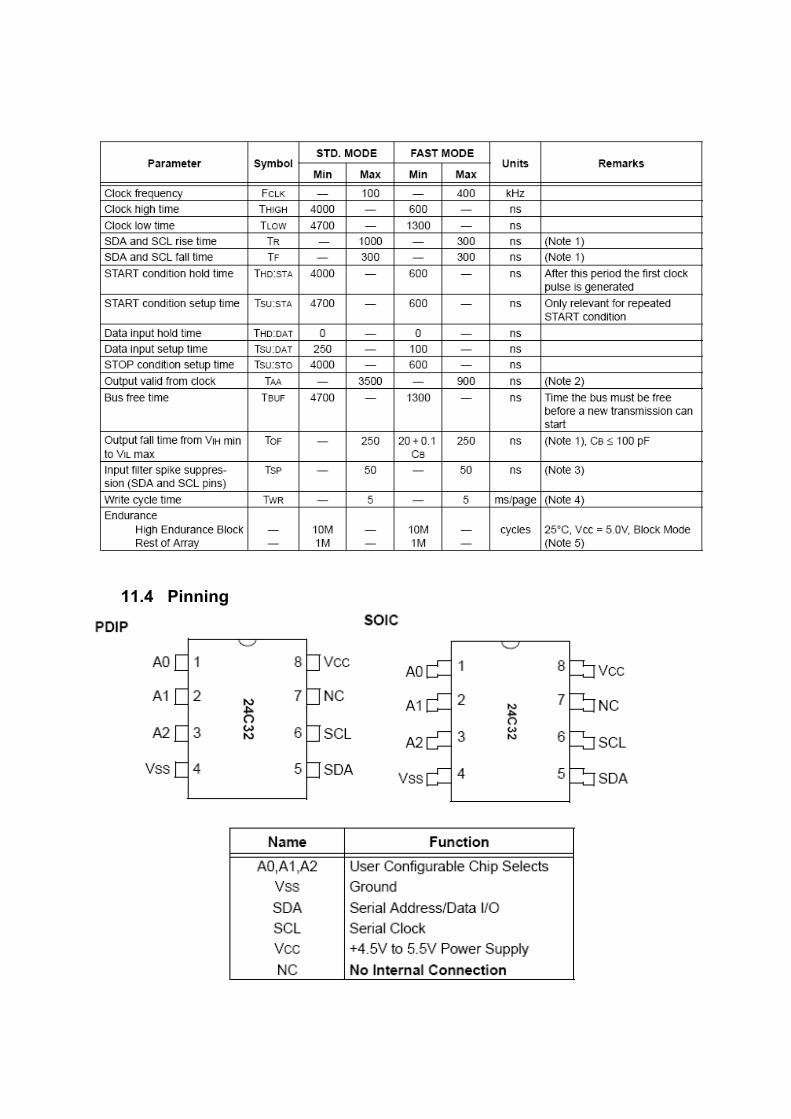
11.4 Pinning
15512K CMOS Serial Flash – MX25L512
15.1 General DescriptionThe MX25L512 is a CMOS 524,288 bit serial Flash memory, which is configured as 65,536 x 8 internally. The MX25L512 feature a serial peripheral interface and software protocol allowing operation on a simple 3-wire bus. The three bus signals are a clock input (SCLK), a serial data input (SI), and a serial data output (SO). SPI access to the device is enabled by CS# input. The MX25L512 provide sequential read operation on whole chip. After program/erase command is issued, auto program/ erase algorithms which program/ erase and verify the specified page or sector/block locations will be executed. Program command is executed on page (256 bytes) basis, and erasecommand is executes on chip or sector (4K-bytes). To provide user with ease of interface, a status register is included to indicate the status of the chip. The status readcommand can be issued to detect completion status of a program or erase operation via WIP bit. When the device is not in operation and CS# is high, it is put in standby mode and draws less than 10uA DC current. The MX25L512 utilize MXIC's proprietary memory cell, which reliably stores memory contents even after 100,000 program and erase cycles.
15.2 FeaturesGENERAL Serial Peripheral Interface (SPI) compatible -- Mode 0 and Mode 3 524,288 x 1 bit structure 16 Equal Sectors with 4K byte each Any Sector can be erased individually Single Power Supply Operation 2.7 to 3.6 volt for read, erase, and program operations Latch-up protected to 100mA from -1V to Vcc +1V Low Vcc write inhibit is from 1.5V to 2.5V
PERFORMANCE High Performance Fast access time: 85MHz serial clock (15pF + 1TTL Load) and 66MHz serial clock
(30pF + 1TTL Load) Fast program time: 1.4ms(typ.) and 5ms(max.)/page (256-byte per page) Fast erase time: 60ms(typ.) and 120ms(max.)/sector (4K-byte per sector) ; 1s(typ.)
and 2s(max.)/chip(512Kb) Low Power Consumption Low active read current: 12mA(max.) at 85MHz, 8mA(max.) at 66MHz and
4mA(max.) at 33MHz Low active programming current: 15mA (max.) Low active erase current: 15mA (max.) Low standby current: 10uA (max.) Deep power-down mode 1uA (typical) Minimum 100,000 erase/program cycles
SOFTWARE FEATURES
Input Data Format 1-byte Command code Block Lock protection The BP0~BP1 status bit defines the size of the area to be software protected
against Program and Erase instructions. Auto Erase and Auto Program Algorithm Automatically erases and verifies data at selected sector Automatically programs and verifies data at selected page by an internal algorithm
that automatically times the program pulse widths (Any page to be programed should have page in the erased state first)
Status Register Feature Electronic Identification JEDEC 2-byte Device ID RES command, 1-byte Device ID
HARDWARE FEATURES SCLK Input Serial clock input SI Input Serial Data Input SO Output Serial Data Output WP# pin Hardware write protection HOLD# pin pause the chip without diselecting the chip PACKAGE 8-pin SOP (150mil) All Pb-free devices are RoHS Compliant
11.3 Absolute Maximum Ratings
16IC DESCRIPTIONS
16.1 LM1117
16.1.1 General DescriptionThe LM1117 is a series of low dropout voltage regulators with a dropout of 1.2V at 800mA of load current. It has the same pin-out as National Semiconductor’s industry standard LM317. The LM1117 is available in an adjustable version, which can set the output voltage from 1.25V to 13.8V with only two external resistors. In addition, it is also available in five fixed voltages, 1.8V, 2.5V, 2.85V, 3.3V, and 5V. The LM1117 offers current limiting and thermal shutdown. Its circuit includes a zener trimmed bandgapreference to as-sure output voltage accuracy to within ±1%. The LM1117 series is available in SOT- 223, TO-220, and TO-252 D-PAK packages. A minimum of 10μF tantalum capacitor is required at the output to improve the transient response and stability.
16.1.2 Features Available in 1.8V, 2.5V, 2.85V, 3.3V, 5V, and Adjustable Versions Space Saving SOT-223 Package Current Limiting and Thermal Protection Output Current 800mA Line Regulation 0.2% (Max) Load Regulation 0.4% (Max) Temperature Range LM1117 0°C to 125°C LM1117I -40°C to 125°C
16.1.3 Applications 2.85V Model for SCSI-2 Active Termination Post Regulator for Switching DC/DC Converter High Efficiency Linear Regulators 15 32” TFT TV Service Manual 10/01/2005 Battery Charger Battery Powered Instrumentation
16.1.4 Absolute Maximum Ratings
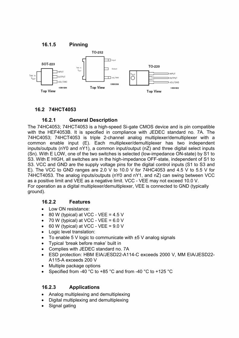
16.1.5 Pinning
16.2 74HCT4053
16.2.1 General DescriptionThe 74HC4053; 74HCT4053 is a high-speed Si-gate CMOS device and is pin compatiblewith the HEF4053B. It is specified in compliance with JEDEC standard no. 7A. The 74HC4053; 74HCT4053 is triple 2-channel analog multiplexer/demultiplexer with acommon enable input (E). Each multiplexer/demultiplexer has two independentinputs/outputs (nY0 and nY1), a common input/output (nZ) and three digital select inputs (Sn). With E LOW, one of the two switches is selected (low-impedance ON-state) by S1 to S3. With E HIGH, all switches are in the high-impedance OFF-state, independent of S1 to S3. VCC and GND are the supply voltage pins for the digital control inputs (S1 to S3 and E). The VCC to GND ranges are 2.0 V to 10.0 V for 74HC4053 and 4.5 V to 5.5 V for74HCT4053. The analog inputs/outputs (nY0 and nY1, and nZ) can swing between VCCas a positive limit and VEE as a negative limit. VCC - VEE may not exceed 10.0 V.For operation as a digital multiplexer/demultiplexer, VEE is connected to GND (typicallyground).
16.2.2 Features Low ON resistance: 80 W (typical) at VCC - VEE = 4.5 V 70 W (typical) at VCC - VEE = 6.0 V 60 W (typical) at VCC - VEE = 9.0 V Logic level translation: To enable 5 V logic to communicate with ±5 V analog signals Typical ‘break before make’ built in Complies with JEDEC standard no. 7A ESD protection: HBM EIA/JESD22-A114-C exceeds 2000 V, MM EIA/JESD22-
A115-A exceeds 200 V Multiple package options Specified from -40 °C to +85 °C and from -40 °C to +125 °C
16.2.3 Applications Analog multiplexing and demultiplexing Digital multiplexing and demultiplexing Signal gating
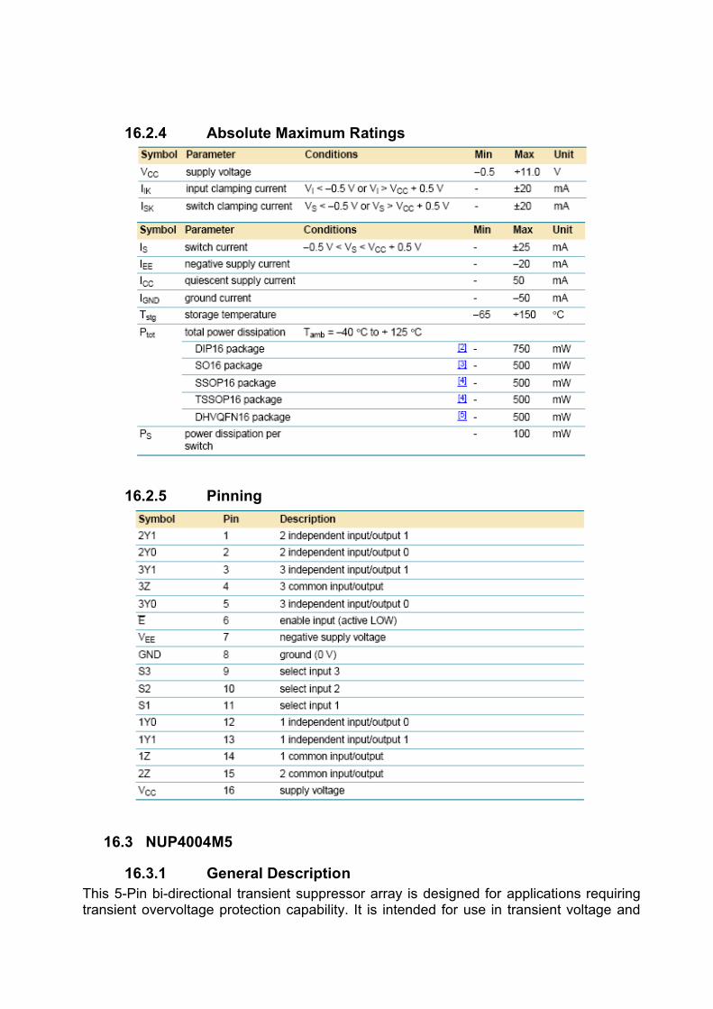
16.2.4 Absolute Maximum Ratings
16.2.5 Pinning
16.3 NUP4004M5
16.3.1 General DescriptionThis 5-Pin bi-directional transient suppressor array is designed for applications requiring transient overvoltage protection capability. It is intended for use in transient voltage and
ESD sensitive equipment such as computers, printers, cell phones, medical equipment, and other applications. Its integrated design provides bi-directional protection for four separate lines using a single TSOP-5 package. This device is ideal for situations where board space is a premium.
16.3.2 Features Bi-directional Protection for Four Lines in a Single TSOP-5 Package Low Leakage Current Low Capacitance Provides ESD Protection for JEDEC Standards JESD22 Machine Model = Class C Human Body Model = Class 3B Provides ESD Protection for IEC 61000-4-2, 15 kV (Air), 8 kV (Contact) This is a Pb-Free Device
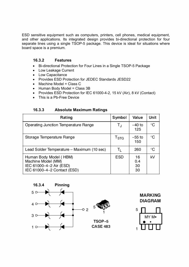
16.3.3 Absolute Maximum Ratings
16.3.4 Pinning
16.4 FDN336P
16.4.1 General DescriptionThe ST24LC21 is a 1K bit electrically erasable programmable memory (EEPROM), organized by 8 bits.This device can operate in two modes: Transmit Only mode and I2C bidirectional mode. When powered, the device is in Transmit Only mode with EEPROM data clocked out from the rising edge of the signal applied on VCLK. The device will switch to the I2C bidirectional mode upon the falling edge of the signal applied on SCLpin. The ST24LC21 cannot switch from the I2C bidirectional mode to the Transmit Only mode (except when the power supply is removed). The device operates with a power supply value as low as 2.5V. Both Plastic Dual-in-Line and Plastic Small Outline packages are available.
16.4.2 Features 1 MILLION ERASE/WRITE CYCLES 40 YEARS DATA RETENTION 2.5V to 5.5V SINGLE SUPPLY VOLTAGE 400k Hz COMPATIBILITY OVER the FULL RANGE of SUPPLY VOLTAGE TWO WIRE SERIAL INTERFACE I2C BUS COMPATIBLE PAGE WRITE (up to 8 BYTES) BYTE, RANDOM and SEQUENTIAL READ MODES SELF TIMED PROGRAMMING CYCLE AUTOMATIC ADDRESS INCREMENTING ENHANCED ESD/LATCH UP PERFORMANCES
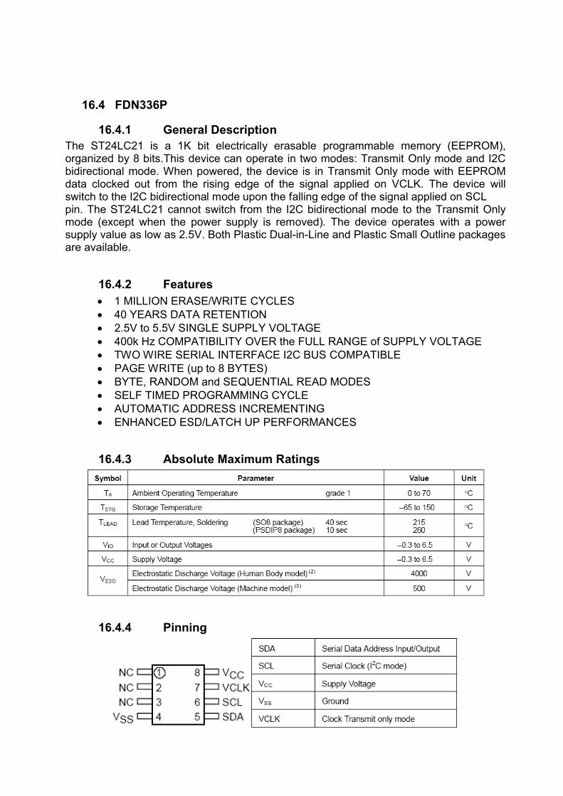
16.4.3 Absolute Maximum Ratings
16.4.4 Pinning
16.5 TL062 -
16.5.1 General DescriptionLow-power JFET-input operational amplifier
16.5.2 Features Very Low Power Consumption Typical Supply Current . . . 200 µA (Per Amplifier) Wide Common-Mode and Differential Voltage Ranges Low Input Bias and Offset Currents Common-Mode Input Voltage Range Includes VCC+ Output Short-Circuit Protection High Input Impedance . . . JFET-Input Stage Internal Frequency Compensation Latch-Up-Free Operation High Slew Rate . . . 3.5 V/µs Typ
16.5.3 Absolute Maximum Ratings
16.5.4 Pinning
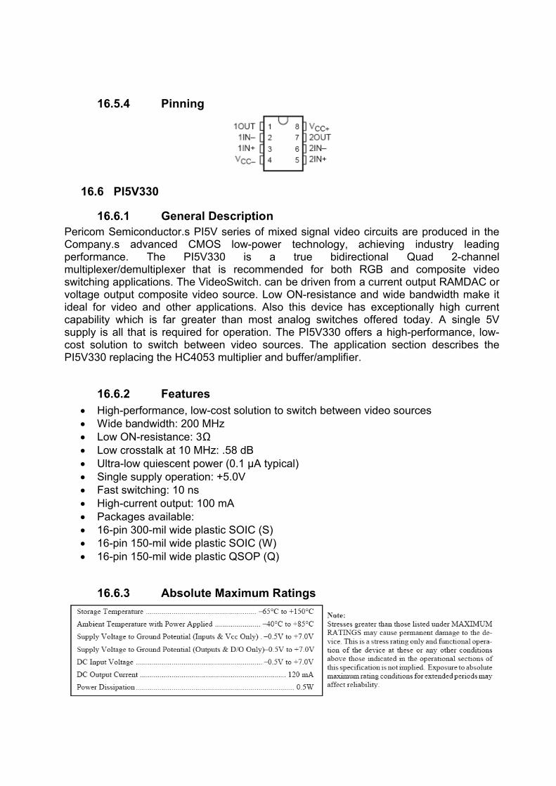
16.6 PI5V330
16.6.1 General DescriptionPericom Semiconductor.s PI5V series of mixed signal video circuits are produced in the Company.s advanced CMOS low-power technology, achieving industry leading performance. The PI5V330 is a true bidirectional Quad 2-channelmultiplexer/demultiplexer that is recommended for both RGB and composite video switching applications. The VideoSwitch. can be driven from a current output RAMDAC or voltage output composite video source. Low ON-resistance and wide bandwidth make it ideal for video and other applications. Also this device has exceptionally high current capability which is far greater than most analog switches offered today. A single 5V supply is all that is required for operation. The PI5V330 offers a high-performance, low-cost solution to switch between video sources. The application section describes the PI5V330 replacing the HC4053 multiplier and buffer/amplifier.
16.6.2 Features High-performance, low-cost solution to switch between video sources Wide bandwidth: 200 MHz Low ON-resistance: 3Ω Low crosstalk at 10 MHz: .58 dB Ultra-low quiescent power (0.1 µA typical) Single supply operation: +5.0V Fast switching: 10 ns High-current output: 100 mA Packages available: 16-pin 300-mil wide plastic SOIC (S) 16-pin 150-mil wide plastic SOIC (W) 16-pin 150-mil wide plastic QSOP (Q)
16.6.3 Absolute Maximum Ratings
16.6.4 Pinning
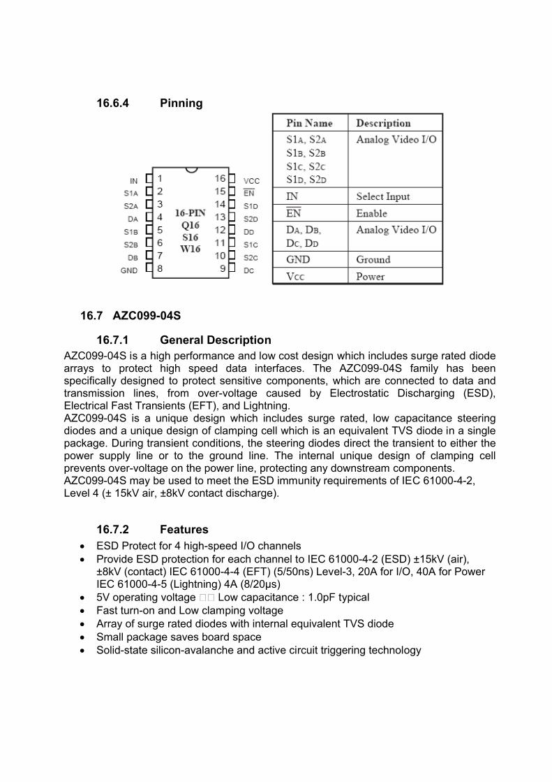
16.7 AZC099-04S
16.7.1 General DescriptionAZC099-04S is a high performance and low cost design which includes surge rated diode arrays to protect high speed data interfaces. The AZC099-04S family has been specifically designed to protect sensitive components, which are connected to data and transmission lines, from over-voltage caused by Electrostatic Discharging (ESD), Electrical Fast Transients (EFT), and Lightning. AZC099-04S is a unique design which includes surge rated, low capacitance steering diodes and a unique design of clamping cell which is an equivalent TVS diode in a single package. During transient conditions, the steering diodes direct the transient to either the power supply line or to the ground line. The internal unique design of clamping cell prevents over-voltage on the power line, protecting any downstream components. AZC099-04S may be used to meet the ESD immunity requirements of IEC 61000-4-2, Level 4 (± 15kV air, ±8kV contact discharge).
16.7.2 Features ESD Protect for 4 high-speed I/O channels Provide ESD protection for each channel to IEC 61000-4-2 (ESD) ±15kV (air),
±8kV (contact) IEC 61000-4-4 (EFT) (5/50ns) Level-3, 20A for I/O, 40A for Power IEC 61000-4-5 (Lightning) 4A (8/20μs)
5V operating voltage Low capacitance : 1.0pF typical Fast turn-on and Low clamping voltage Array of surge rated diodes with internal equivalent TVS diode Small package saves board space Solid-state silicon-avalanche and active circuit triggering technology
16.7.3 Absolute Maximum Ratings
16.7.4 Pinning
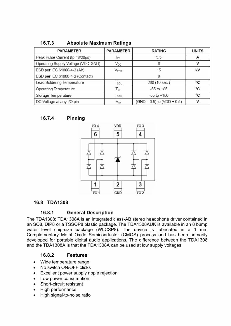
16.8 TDA1308
16.8.1 General DescriptionThe TDA1308; TDA1308A is an integrated class-AB stereo headphone driver contained inan SO8, DIP8 or a TSSOP8 plastic package. The TDA1308AUK is available in an 8 bumpwafer level chip-size package (WLCSP8). The device is fabricated in a 1 mmComplementary Metal Oxide Semiconductor (CMOS) process and has been primarilydeveloped for portable digital audio applications. The difference between the TDA1308 and the TDA1308A is that the TDA1308A can be used at low supply voltages.
16.8.2 Features Wide temperature range No switch ON/OFF clicks Excellent power supply ripple rejection Low power consumption Short-circuit resistant High performance High signal-to-noise ratio
High slew rate Low distortion Large output voltage swing
16.8.3 Absolute Maximum Ratings
16.8.4 Pinning
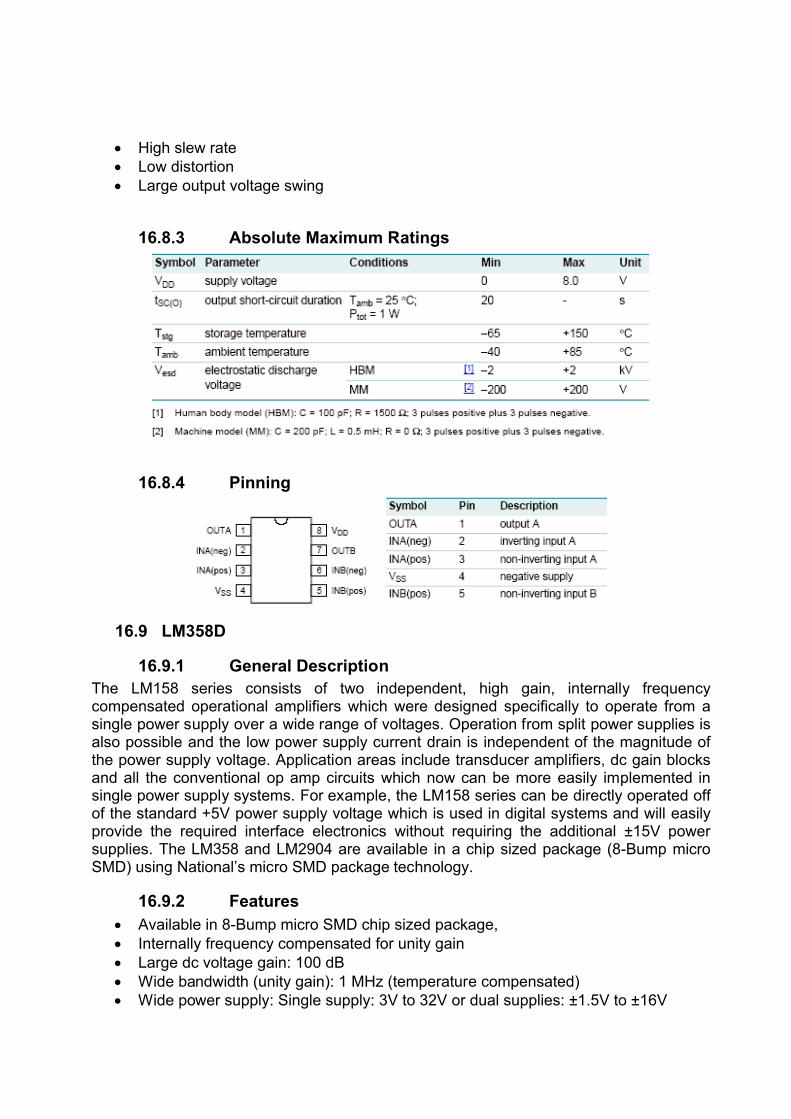
16.9 LM358D
16.9.1 General DescriptionThe LM158 series consists of two independent, high gain, internally frequency compensated operational amplifiers which were designed specifically to operate from a single power supply over a wide range of voltages. Operation from split power supplies is also possible and the low power supply current drain is independent of the magnitude of the power supply voltage. Application areas include transducer amplifiers, dc gain blocks and all the conventional op amp circuits which now can be more easily implemented in single power supply systems. For example, the LM158 series can be directly operated off of the standard +5V power supply voltage which is used in digital systems and will easily provide the required interface electronics without requiring the additional ±15V power supplies. The LM358 and LM2904 are available in a chip sized package (8-Bump micro SMD) using National’s micro SMD package technology.
16.9.2 Features Available in 8-Bump micro SMD chip sized package, Internally frequency compensated for unity gain Large dc voltage gain: 100 dB Wide bandwidth (unity gain): 1 MHz (temperature compensated) Wide power supply: Single supply: 3V to 32V or dual supplies: ±1.5V to ±16V
Low supply current drain (500 µA)—essentially independent of supply voltage Low input offset voltage: 2 mV Input common-mode voltage range includes ground Differential input voltage range equal to the power supply voltage Large output voltage swing
16.9.3 Absolute Maximum Ratings
16.9.4 Pinning
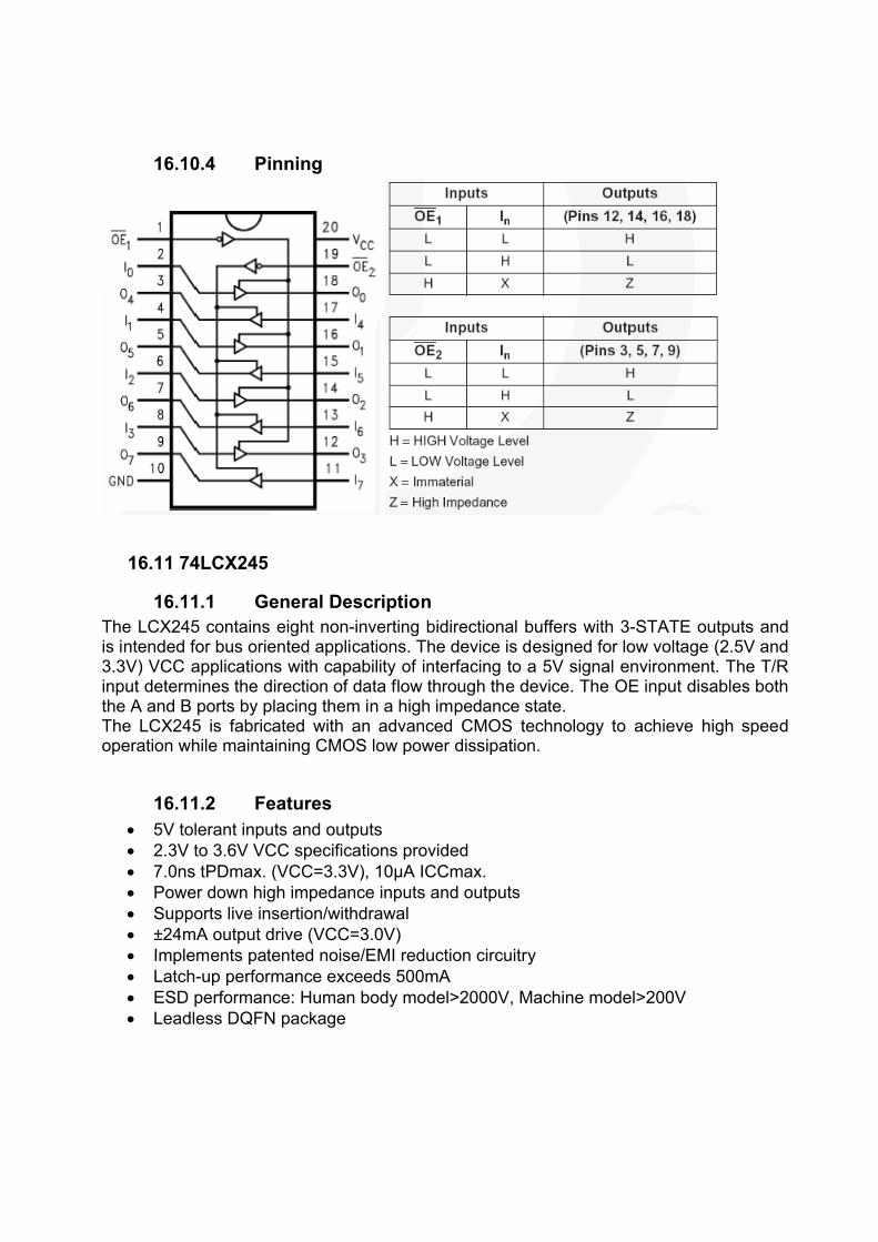
16.10 74LCX244
16.10.1 General DescriptionThe LCX244 contains eight non-inverting buffers with 3-STATE outputs. The device may be employed as a memory address driver, clock driver and bus-oriented
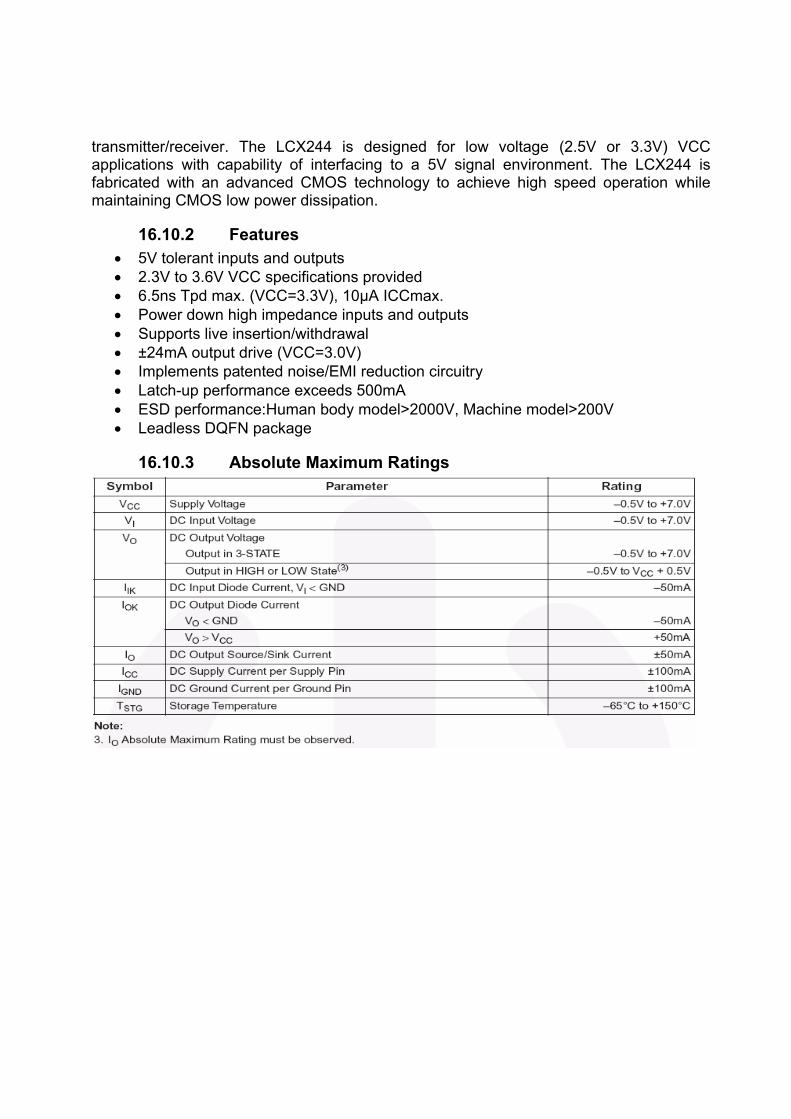
transmitter/receiver. The LCX244 is designed for low voltage (2.5V or 3.3V) VCCapplications with capability of interfacing to a 5V signal environment. The LCX244 is fabricated with an advanced CMOS technology to achieve high speed operation while maintaining CMOS low power dissipation.
16.10.2 Features 5V tolerant inputs and outputs 2.3V to 3.6V VCC specifications provided 6.5ns Tpd max. (VCC=3.3V), 10µA ICCmax. Power down high impedance inputs and outputs Supports live insertion/withdrawal ±24mA output drive (VCC=3.0V) Implements patented noise/EMI reduction circuitry Latch-up performance exceeds 500mA ESD performance:Human body model>2000V, Machine model>200V Leadless DQFN package
16.10.3 Absolute Maximum Ratings
16.10.4 Pinning
16.11 74LCX245
16.11.1 General DescriptionThe LCX245 contains eight non-inverting bidirectional buffers with 3-STATE outputs and is intended for bus oriented applications. The device is designed for low voltage (2.5V and 3.3V) VCC applications with capability of interfacing to a 5V signal environment. The T/R input determines the direction of data flow through the device. The OE input disables both the A and B ports by placing them in a high impedance state.The LCX245 is fabricated with an advanced CMOS technology to achieve high speed operation while maintaining CMOS low power dissipation.
16.11.2 Features 5V tolerant inputs and outputs 2.3V to 3.6V VCC specifications provided 7.0ns tPDmax. (VCC=3.3V), 10µA ICCmax. Power down high impedance inputs and outputs Supports live insertion/withdrawal ±24mA output drive (VCC=3.0V) Implements patented noise/EMI reduction circuitry Latch-up performance exceeds 500mA ESD performance: Human body model>2000V, Machine model>200V Leadless DQFN package
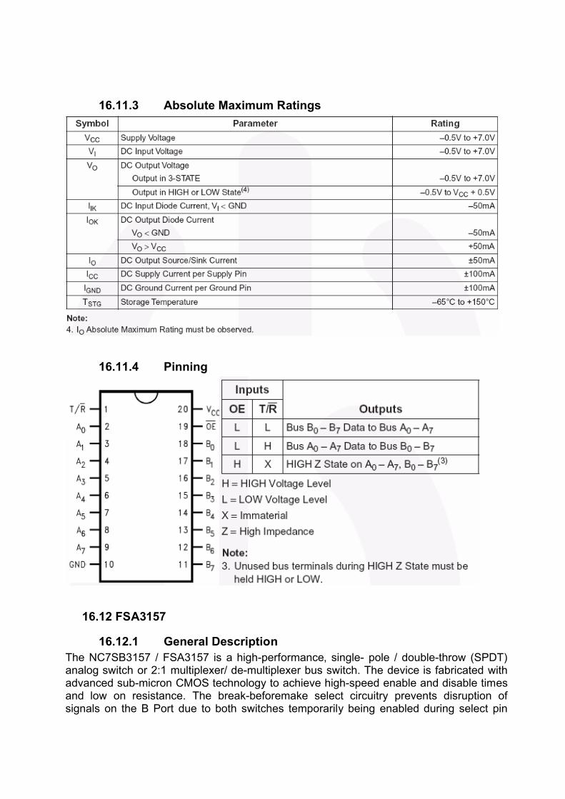
16.11.3 Absolute Maximum Ratings
16.11.4 Pinning
16.12 FSA3157
16.12.1 General DescriptionThe NC7SB3157 / FSA3157 is a high-performance, single- pole / double-throw (SPDT) analog switch or 2:1 multiplexer/ de-multiplexer bus switch. The device is fabricated with advanced sub-micron CMOS technology to achieve high-speed enable and disable times and low on resistance. The break-beforemake select circuitry prevents disruption of signals on the B Port due to both switches temporarily being enabled during select pin
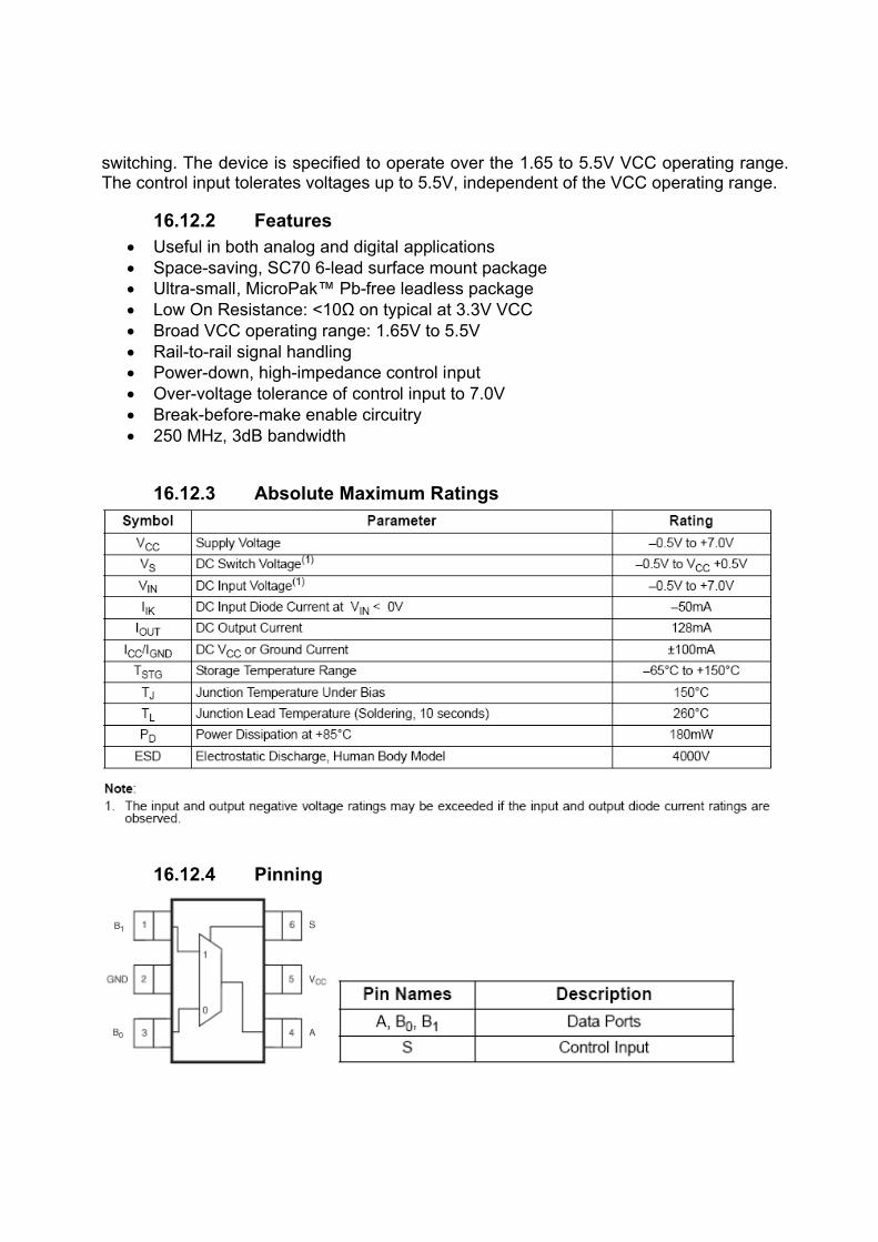
switching. The device is specified to operate over the 1.65 to 5.5V VCC operating range. The control input tolerates voltages up to 5.5V, independent of the VCC operating range.
16.12.2 Features Useful in both analog and digital applications Space-saving, SC70 6-lead surface mount package Ultra-small, MicroPak™ Pb-free leadless package Low On Resistance: <10Ω on typical at 3.3V VCC Broad VCC operating range: 1.65V to 5.5V Rail-to-rail signal handling Power-down, high-impedance control input Over-voltage tolerance of control input to 7.0V Break-before-make enable circuitry 250 MHz, 3dB bandwidth
16.12.3 Absolute Maximum Ratings
16.12.4 Pinning
16.13 TSH343
16.13.1 General Description
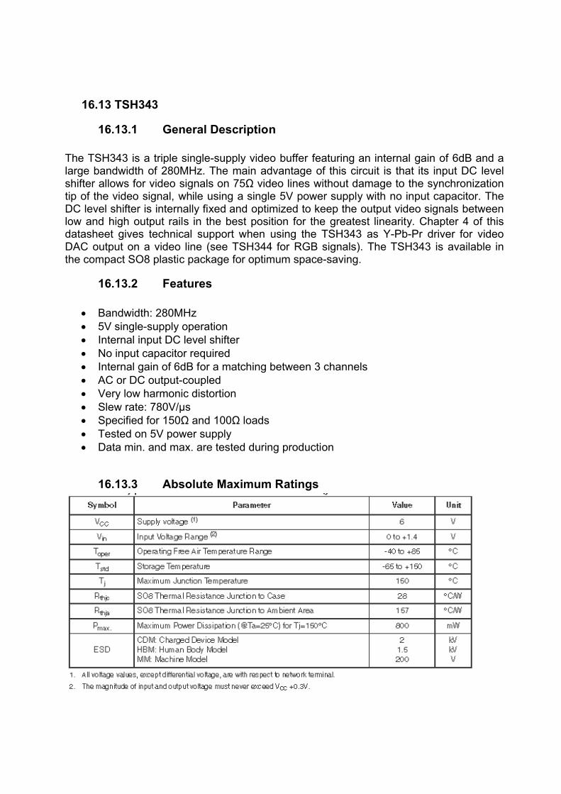
The TSH343 is a triple single-supply video buffer featuring an internal gain of 6dB and a large bandwidth of 280MHz. The main advantage of this circuit is that its input DC level shifter allows for video signals on 75Ω video lines without damage to the synchronization tip of the video signal, while using a single 5V power supply with no input capacitor. The DC level shifter is internally fixed and optimized to keep the output video signals between low and high output rails in the best position for the greatest linearity. Chapter 4 of this datasheet gives technical support when using the TSH343 as Y-Pb-Pr driver for video DAC output on a video line (see TSH344 for RGB signals). The TSH343 is available in the compact SO8 plastic package for optimum space-saving.
16.13.2 Features
Bandwidth: 280MHz 5V single-supply operation Internal input DC level shifter No input capacitor required Internal gain of 6dB for a matching between 3 channels AC or DC output-coupled Very low harmonic distortion Slew rate: 780V/μs Specified for 150Ω and 100Ω loads Tested on 5V power supply Data min. and max. are tested during production
16.13.3 Absolute Maximum Ratings
16.13.4 Pinning
16.14 MT48LC4M16A2TG8E
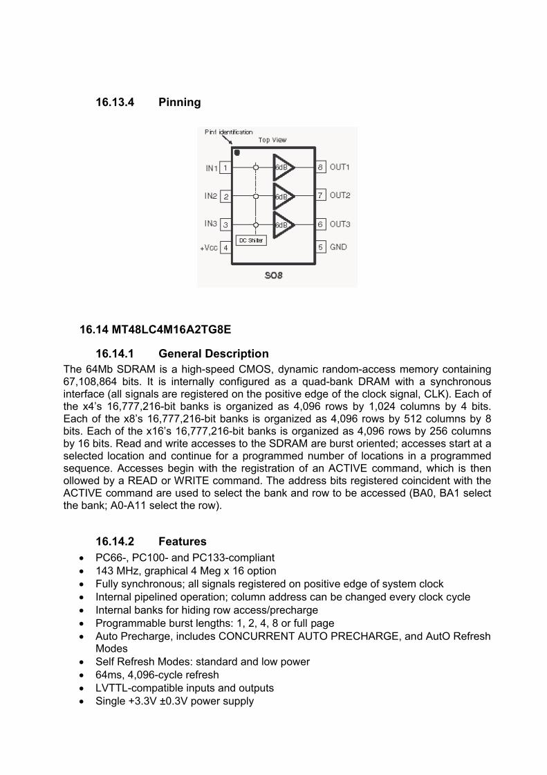
16.14.1 General DescriptionThe 64Mb SDRAM is a high-speed CMOS, dynamic random-access memory containing 67,108,864 bits. It is internally configured as a quad-bank DRAM with a synchronous interface (all signals are registered on the positive edge of the clock signal, CLK). Each of the x4’s 16,777,216-bit banks is organized as 4,096 rows by 1,024 columns by 4 bits. Each of the x8’s 16,777,216-bit banks is organized as 4,096 rows by 512 columns by 8bits. Each of the x16’s 16,777,216-bit banks is organized as 4,096 rows by 256 columns by 16 bits. Read and write accesses to the SDRAM are burst oriented; accesses start at a selected location and continue for a programmed number of locations in a programmed sequence. Accesses begin with the registration of an ACTIVE command, which is thenollowed by a READ or WRITE command. The address bits registered coincident with the ACTIVE command are used to select the bank and row to be accessed (BA0, BA1 select the bank; A0-A11 select the row).
16.14.2 Features PC66-, PC100- and PC133-compliant 143 MHz, graphical 4 Meg x 16 option Fully synchronous; all signals registered on positive edge of system clock Internal pipelined operation; column address can be changed every clock cycle Internal banks for hiding row access/precharge Programmable burst lengths: 1, 2, 4, 8 or full page Auto Precharge, includes CONCURRENT AUTO PRECHARGE, and AutO Refresh
Modes Self Refresh Modes: standard and low power 64ms, 4,096-cycle refresh LVTTL-compatible inputs and outputs Single +3.3V ±0.3V power supply
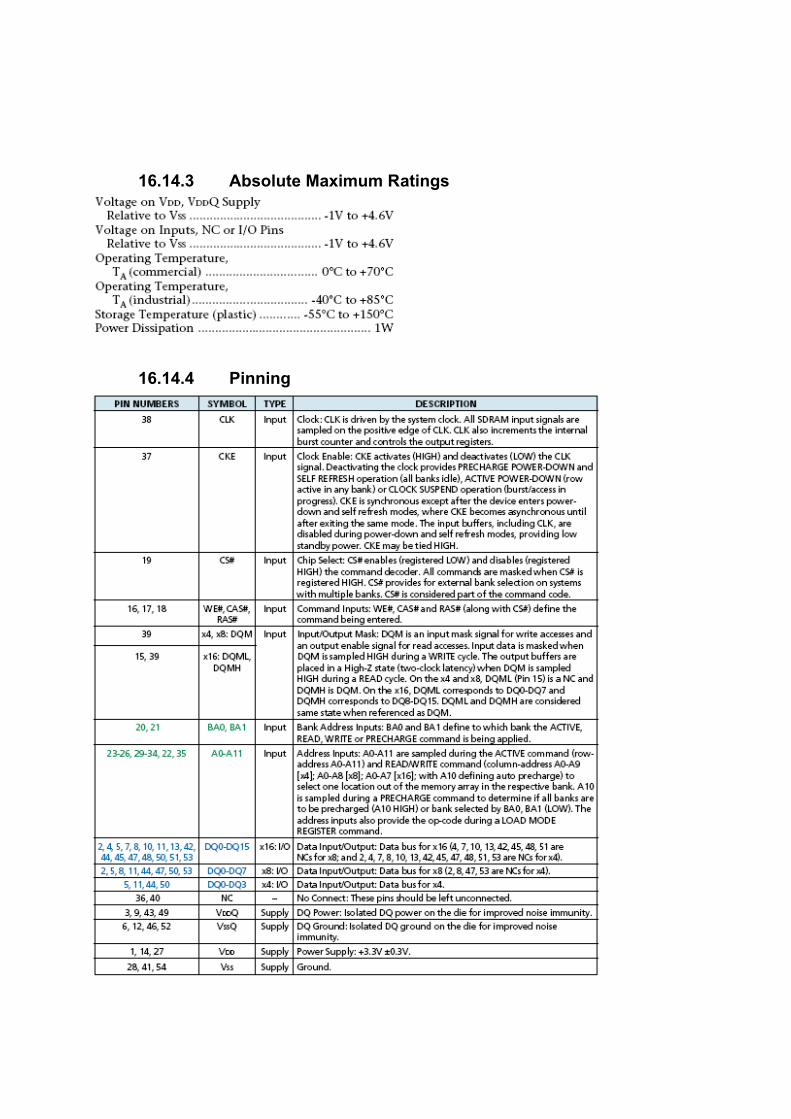
16.14.3 Absolute Maximum Ratings
16.14.4 Pinning
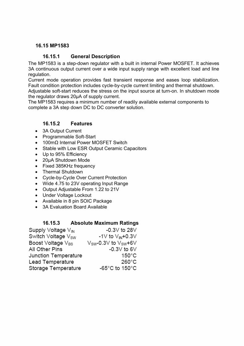
16.15 MP1583
16.15.1 General DescriptionThe MP1583 is a step-down regulator with a built in internal Power MOSFET. It achieves 3A continuous output current over a wide input supply range with excellent load and lineregulation.Current mode operation provides fast transient response and eases loop stabilization.Fault condition protection includes cycle-by-cycle current limiting and thermal shutdown.Adjustable soft-start reduces the stress on the input source at turn-on. In shutdown mode the regulator draws 20µA of supply current.The MP1583 requires a minimum number of readily available external components tocomplete a 3A step down DC to DC converter solution.
16.15.2 Features 3A Output Current Programmable Soft-Start 100mΩ Internal Power MOSFET Switch Stable with Low ESR Output Ceramic Capacitors Up to 95% Efficiency 20µA Shutdown Mode Fixed 385KHz frequency Thermal Shutdown Cycle-by-Cycle Over Current Protection Wide 4.75 to 23V operating Input Range Output Adjustable From 1.22 to 21V Under Voltage Lockout Available in 8 pin SOIC Package 3A Evaluation Board Available
16.15.3 Absolute Maximum Ratings
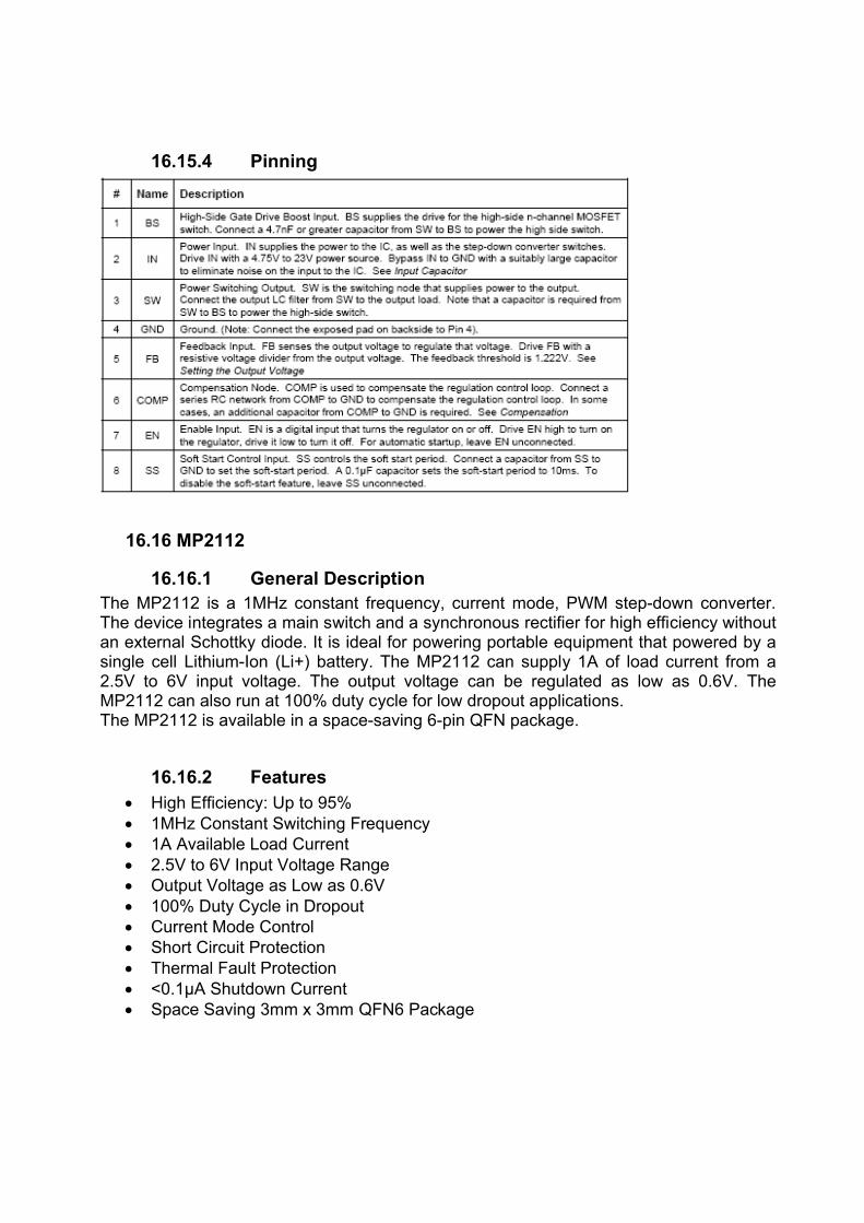
16.15.4 Pinning
16.16 MP2112
16.16.1 General DescriptionThe MP2112 is a 1MHz constant frequency, current mode, PWM step-down converter. The device integrates a main switch and a synchronous rectifier for high efficiency withoutan external Schottky diode. It is ideal for powering portable equipment that powered by asingle cell Lithium-Ion (Li+) battery. The MP2112 can supply 1A of load current from a2.5V to 6V input voltage. The output voltage can be regulated as low as 0.6V. The MP2112 can also run at 100% duty cycle for low dropout applications.The MP2112 is available in a space-saving 6-pin QFN package.
16.16.2 Features High Efficiency: Up to 95% 1MHz Constant Switching Frequency 1A Available Load Current 2.5V to 6V Input Voltage Range Output Voltage as Low as 0.6V 100% Duty Cycle in Dropout Current Mode Control Short Circuit Protection Thermal Fault Protection <0.1µA Shutdown Current Space Saving 3mm x 3mm QFN6 Package
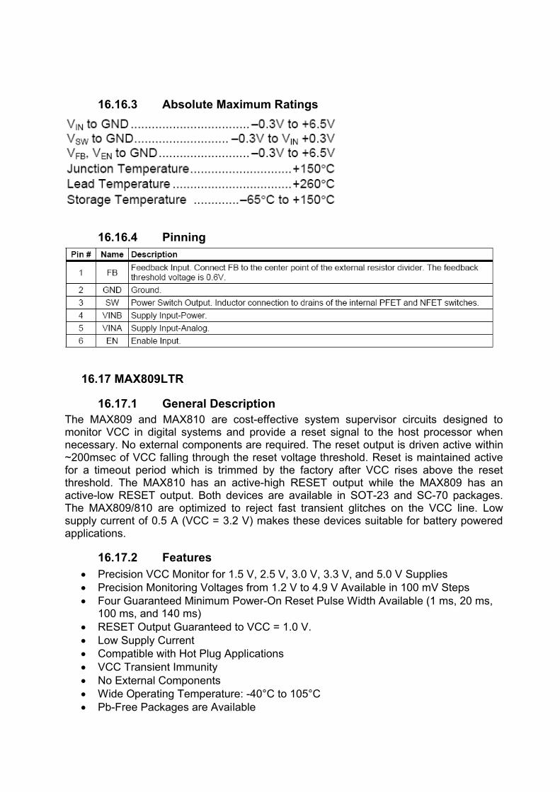
16.16.3 Absolute Maximum Ratings
16.16.4 Pinning
16.17 MAX809LTR
16.17.1 General DescriptionThe MAX809 and MAX810 are cost-effective system supervisor circuits designed to monitor VCC in digital systems and provide a reset signal to the host processor when necessary. No external components are required. The reset output is driven active within ~200msec of VCC falling through the reset voltage threshold. Reset is maintained active for a timeout period which is trimmed by the factory after VCC rises above the reset threshold. The MAX810 has an active-high RESET output while the MAX809 has an active-low RESET output. Both devices are available in SOT-23 and SC-70 packages.The MAX809/810 are optimized to reject fast transient glitches on the VCC line. Low supply current of 0.5 A (VCC = 3.2 V) makes these devices suitable for battery powered applications.
16.17.2 Features Precision VCC Monitor for 1.5 V, 2.5 V, 3.0 V, 3.3 V, and 5.0 V Supplies Precision Monitoring Voltages from 1.2 V to 4.9 V Available in 100 mV Steps Four Guaranteed Minimum Power-On Reset Pulse Width Available (1 ms, 20 ms,
100 ms, and 140 ms) RESET Output Guaranteed to VCC = 1.0 V. Low Supply Current Compatible with Hot Plug Applications VCC Transient Immunity No External Components Wide Operating Temperature: -40°C to 105°C Pb-Free Packages are Available
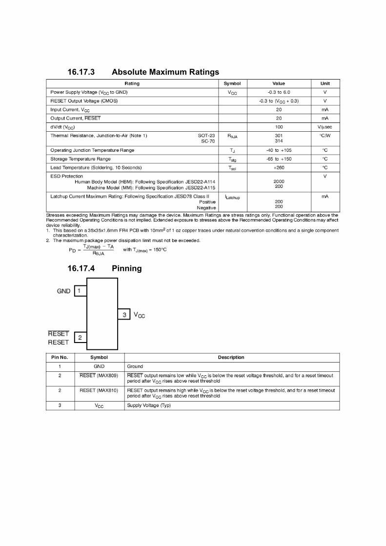
16.17.3 Absolute Maximum Ratings
16.17.4 Pinning
17SERVICE MENU SETTINGSIn order to reach service menu, First Press “MENU” Then press the remote control code, which is “4725”. In DTV mode, first press “MENU” and select “TV SETUP”. Then, press “4725”.
17.1 Video SetupPanel Info <..................................>
32_LC_SAC1Blue Background <.....>
If “Menu” selected, “Blue Background” item is seen in “Feature”menu.If “Yes” selected, “Blue Background” is on and not seen in
“Feature” menuFilm Mode <.....>
If “Yes” selected, “Film Mode” feature is active.Dynamic Contrast <.....>
If “Yes” selected, “Dynamic Contrast” feature is active.Game Mode <...........>
If “Yes” selected, “Game Mode” feature is activeSRGB For PC <...........>
If “Yes” selected, PCs can use SRGB option.Dynamic Noise Reduction<...........>
If “Yes” selected, “Dynamic Noise Reduction” feature is activeWSS Option<...........>
If “Yes” selected, WSS Option can be used
17.2 AudioSetupBG<.....>
EuropeNew ZellandAustraliaNo
DK<.....>I<.....>L<.....>Equalizer <.....>
If “Yes” selected, “Equalizer” item is seen in “Sound” menu.Headphone <.....>
If “Yes” selected, “Headphone” item is seen in “Sound” menu.Power On/Off Melody <.....>
If “Yes” selected, when power on/off conditions, the power on/off melody can be heard.
Dynamic Bass <.....>Value between 0 to 12Effect<.....> Value between 0 to 7Audio Delay ,offset <.....> Value between 0 to 190Audio Setup Cont...2
Carrier mute<.......> Value between 0 to 28Headphone Sound Select <.......>
Always Active SelectAlways Inactive SelectMenuAlways Main MenuAlways PIP/PAP Window
Sound Mode Detect Time <.......> Value between 0 to 255Noise Reduction Threshold <.......> Value between 0 to 255Noise Reduction Time <.......> Value between 0 to 15AVL Attack Time <.......> Value between 0 to 255AVL Release Time <.......> Value between 0 to 255
Prescales ( AVL On)FM Prescale<.......> Value between 0 to 255AM Prescale <.......> Value between 0 to 255NICAM Prescale <.......> Value between 0 to 255SCART Prescale <.......> Value between 0 to 255FAV Prescale <.......> Value between 0 to 255DTV Prescale <.......> Value between 0 to 255HDMI Prescale <.......> Value between 0 to 255YPbPr/PC Prescale <.......> Value between 0 to 255An. USB Prescale <.......> Value between 0 to 255Dig. USB Prescale <.......> Value between 0 to 255
Prescales ( AVL Off)FM Prescale<.......> Value between 0 to 255AM Prescale <.......> Value between 0 to 255NICAM Prescale <.......> Value between 0 to 255SCART Prescale <.......> Value between 0 to 255FAV Prescale <.......> Value between 0 to 255DTV Prescale <.......> Value between 0 to 255HDMI Prescale <.......> Value between 0 to 255YPbPr/PC Prescale <.......> Value between 0 to 255An. USB Prescale <.......> Value between 0 to 255Dig. USB Prescale <.......> Value between 0 to 255
Clipping Levels ( AVL On)FM Clipping <.......> Value between 0 to 255AM Clipping <.......> Value between 0 to 255NICAM Clipping <.......> Value between 0 to 255SCART Clipping <.......> Value between 0 to 255FAV Clipping <.......> Value between 0 to 255DTV Clipping <.......> Value between 0 to 255HDMI Clipping <.......> Value between 0 to 255YPbPr/PC Clipping <.......> Value between 0 to 255An. USB Clipping <.......> Value between 0 to 255Dig. USB Clipping <.......> Value between 0 to 255
Clipping Levels ( AVL Off)FM Clipping <.......> Value between 0 to 255AM Clipping <.......> Value between 0 to 255NICAM Clipping <.......> Value between 0 to 255
SCART Clipping <.......> Value between 0 to 255FAV Clipping <.......> Value between 0 to 255DTV Clipping <.......> Value between 0 to 255HDMI Clipping <.......> Value between 0 to 255YPbPr/PC Clipping <.......> Value between 0 to 255An. USB Clipping <.......> Value between 0 to 255Dig. USB Clipping <.......> Value between 0 to 255
17.3 Service Scan/Tuning SetupFirst Search for L/L’ <.......>ATS Delay Time (ms) <.......> Value between 0 to +200Main Tuner Setup
Tuner TypeLC_TDTC_GXX1DThomson DTT7543XPhilips TD1318AF-3Samsung DTOs403LH172AGeneric ( Analog Only)
Control Byte <.......> Value between 0 to +255BSW1 <.......> Value between 0 to +255BSW2 <.......> Value between 0 to +255BSW3 <.......> Value between 0 to +255Low-Mid – Low Byte <.......>Low-Mid – High Byte <.......>Mid-High – Low Byte <.......>Mid-High – High Byte <.......>
S Band TOP <.......>VIF TOP <.......> Value between 0 to +15VIF TOP SECAM <.......> Value between 0 to +15VIF TOP DK<.......> Value between 0 to +15Synch Threshold<.......> Value between 0 to +40
17.4 OptionsOptions-1
Power UpStandbyLast state
TV Open ModeSource1st TVLast Tv
First APS <.......> If “Yes” selected, first time TV opens by asking APS.
APS Volume <.......> Value between 0 to +63Burn In Mode <.......>
If “Yes” selected, TV opens with Burn-In mode. This mode is used in manufacturing.
APS Test
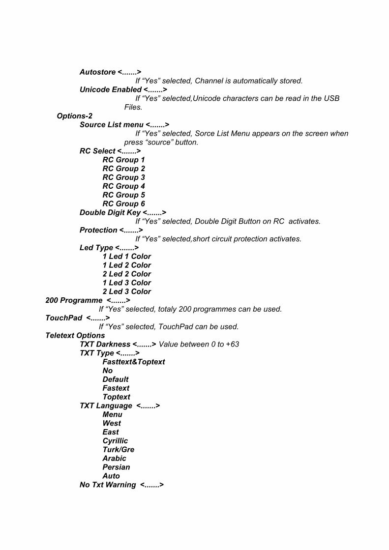
Autostore <.......>If “Yes” selected, Channel is automatically stored.
Unicode Enabled <.......>If “Yes” selected,Unicode characters can be read in the USB
Files.Options-2
Source List menu <.......>If “Yes” selected, Sorce List Menu appears on the screen when
press “source” button.RC Select <.......>
RC Group 1RC Group 2RC Group 3RC Group 4RC Group 5RC Group 6
Double Digit Key <.......>If “Yes” selected, Double Digit Button on RC activates.
Protection <.......> If “Yes” selected,short circuit protection activates.
Led Type <.......>1 Led 1 Color1 Led 2 Color2 Led 2 Color1 Led 3 Color2 Led 3 Color
200 Programme <.......> If “Yes” selected, totaly 200 programmes can be used.
TouchPad <.......> If “Yes” selected, TouchPad can be used.
Teletext OptionsTXT Darkness <.......> Value between 0 to +63TXT Type <.......>
Fasttext&ToptextNoDefaultFastextToptext
TXT Language <.......>MenuWest East CyrillicTurk/GreArabicPersianAuto
No Txt Warning <.......>
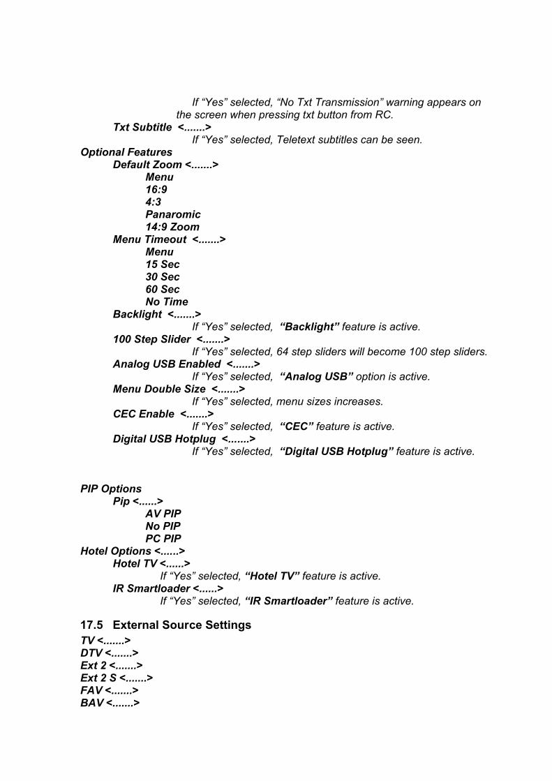
If “Yes” selected, “No Txt Transmission” warning appears on the screen when pressing txt button from RC.
Txt Subtitle <.......>If “Yes” selected, Teletext subtitles can be seen.
Optional FeaturesDefault Zoom <.......>
Menu16:94:3Panaromic14:9 Zoom
Menu Timeout <.......>Menu15 Sec30 Sec60 SecNo Time
Backlight <.......>If “Yes” selected, “Backlight” feature is active.
100 Step Slider <.......>If “Yes” selected, 64 step sliders will become 100 step sliders.
Analog USB Enabled <.......>If “Yes” selected, “Analog USB” option is active.
Menu Double Size <.......>If “Yes” selected, menu sizes increases.
CEC Enable <.......>If “Yes” selected, “CEC” feature is active.
Digital USB Hotplug <.......>If “Yes” selected, “Digital USB Hotplug” feature is active.
PIP OptionsPip <......>
AV PIPNo PIPPC PIP
Hotel Options <......>Hotel TV <......>
If “Yes” selected, “Hotel TV” feature is active.IR Smartloader <......>
If “Yes” selected, “IR Smartloader” feature is active.
17.5 External Source SettingsTV <.......>DTV <.......>Ext 2 <.......>Ext 2 S <.......>FAV <.......>BAV <.......>
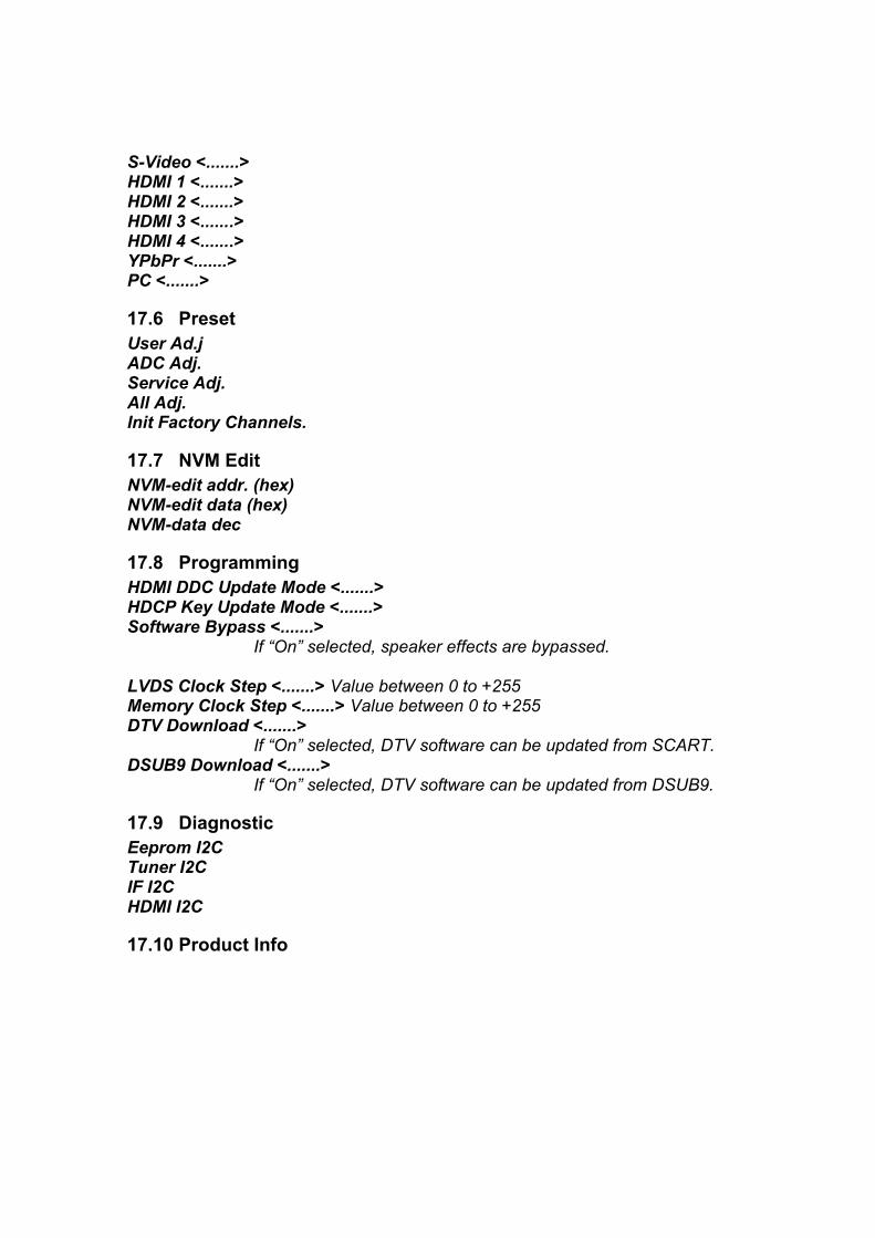
S-Video <.......>HDMI 1 <.......>HDMI 2 <.......>HDMI 3 <.......>HDMI 4 <.......>YPbPr <.......>PC <.......>
17.6 PresetUser Ad.jADC Adj.Service Adj.All Adj.Init Factory Channels.
17.7 NVM EditNVM-edit addr. (hex)NVM-edit data (hex)NVM-data dec
17.8 ProgrammingHDMI DDC Update Mode <.......>HDCP Key Update Mode <.......>Software Bypass <.......>
If “On” selected, speaker effects are bypassed.
LVDS Clock Step <.......> Value between 0 to +255Memory Clock Step <.......> Value between 0 to +255DTV Download <.......>
If “On” selected, DTV software can be updated from SCART.DSUB9 Download <.......>
If “On” selected, DTV software can be updated from DSUB9.
17.9 DiagnosticEeprom I2CTuner I2CIF I2CHDMI I2C
17.10 Product Info
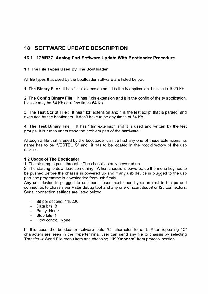
18 SOFTWARE UPDATE DESCRIPTION
16.1 17MB37 Analog Part Software Update With Bootloader Procedure
1.1 The File Types Used By The Bootloader
All file types that used by the bootloader software are listed below:
1. The Binary File : It has “.bin” extension and it is the tv application. Its size is 1920 Kb.
2. The Config Binary File : It has “.cin extension and it is the config of the tv application. Its size may be 64 Kb or a few times 64 Kb.
3. The Test Script File : It has “.txt” extension and it is the test script that is parsed and executed by the bootloader. It don’t have to be any times of 64 Kb.
4. The Test Binary File : It has “.tin” extension and it is used and written by the test groups. It is run to understand the problem part of the hardware.
Alltough a file that is used by the bootloader can be had any one of these extensions, its name has to be “VESTEL_S” and it has to be located in the root directory of the usb device.
1.2 Usage of The Bootloader1. The starting to pass through : The chassis is only powered up.2. The starting to download something : When chassis is powered up the menu key has to be pushed.Before the chassis is powered up and if any usb device is plugged to the usb port, the programme is downloaded from usb firstly.Any usb device is plugged to usb port , user must open hyperterminal in the pc and connect pc to chassis via Mstar debug tool and any one of scart,dsub9 or I2c connectors. Serial connection settings are listed below:
- Bit per second: 115200 - Data bits: 8 - Parity: None- Stop bits: 1- Flow control: None
In this case the bootloader sofware puts “C” character to uart. After repeating “C” characters are seen in the hyperterminal user can send any file to chassis by selecting Transfer -> Send File menu item and choosing “1K Xmodem” from protocol section.
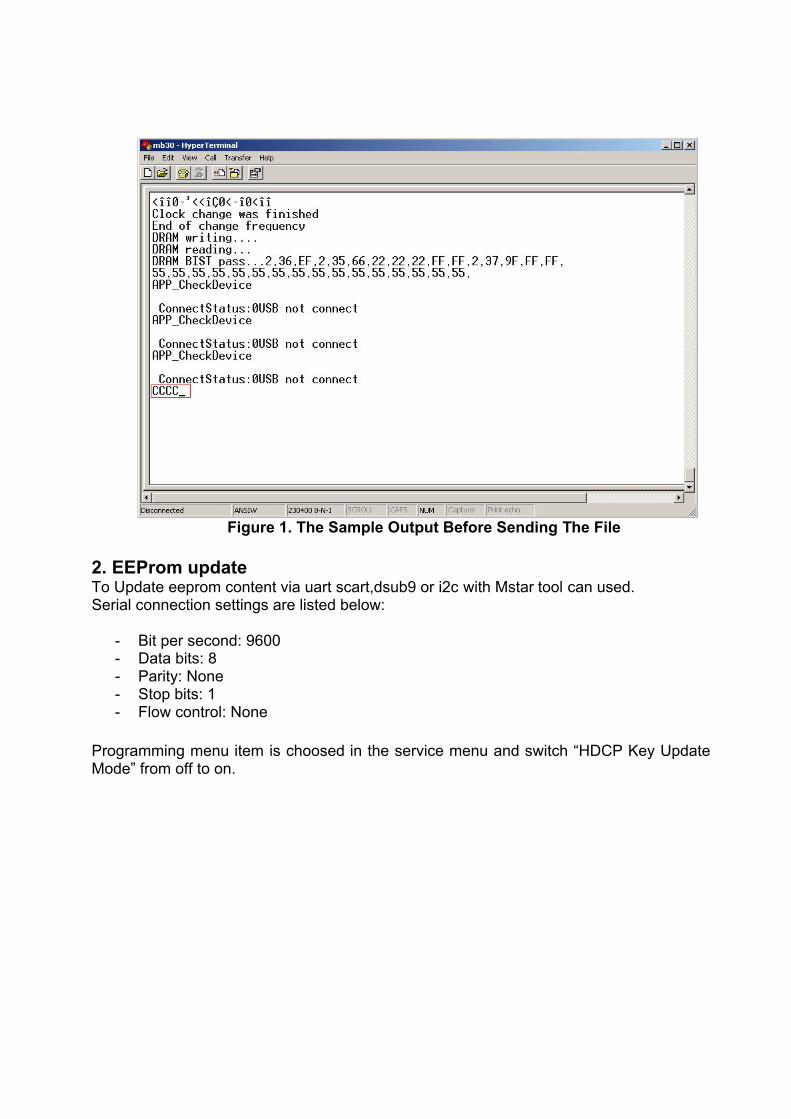
Figure 1. The Sample Output Before Sending The File
2. EEProm update To Update eeprom content via uart scart,dsub9 or i2c with Mstar tool can used.Serial connection settings are listed below:
- Bit per second: 9600 - Data bits: 8 - Parity: None- Stop bits: 1- Flow control: None
Programming menu item is choosed in the service menu and switch “HDCP Key Update Mode” from off to on.
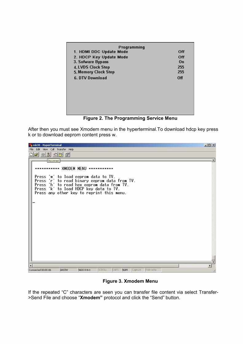
Figure 2. The Programming Service Menu
After then you must see Xmodem menu in the hyperterminal.To download hdcp key press k or to download eeprom content press w.
Figure 3. Xmodem Menu
If the repeated “C” characters are seen you can transfer file content via select Transfer->Send File and choose “Xmodem” protocol and click the “Send” button.
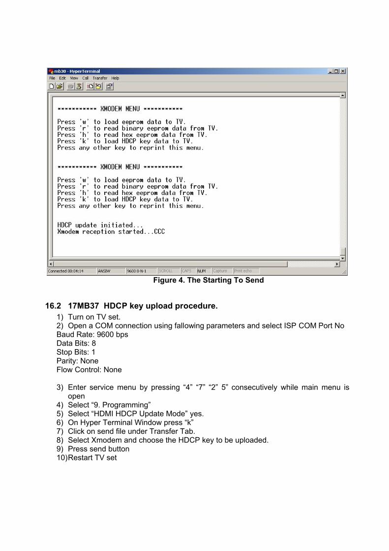
Figure 4. The Starting To Send
16.2 17MB37 HDCP key upload procedure.1) Turn on TV set.2) Open a COM connection using fallowing parameters and select ISP COM Port NoBaud Rate: 9600 bpsData Bits: 8Stop Bits: 1Parity: NoneFlow Control: None
3) Enter service menu by pressing “4” “7” “2” 5” consecutively while main menu is open
4) Select “9. Programming”5) Select “HDMI HDCP Update Mode” yes.6) On Hyper Terminal Window press “k”7) Click on send file under Transfer Tab.8) Select Xmodem and choose the HDCP key to be uploaded.9) Press send button10)Restart TV set
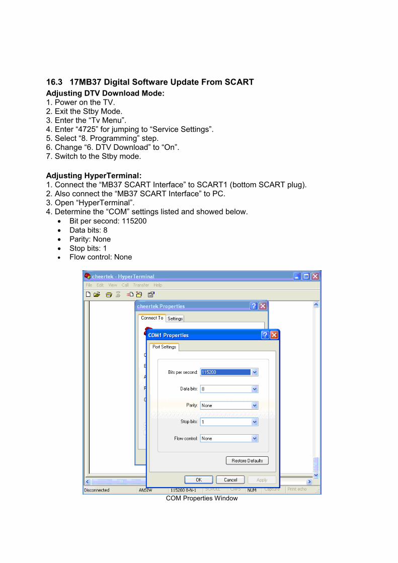
16.3 17MB37 Digital Software Update From SCARTAdjusting DTV Download Mode: 1. Power on the TV. 2. Exit the Stby Mode.3. Enter the “Tv Menu”. 4. Enter “4725” for jumping to “Service Settings”. 5. Select “8. Programming” step. 6. Change “6. DTV Download” to “On”. 7. Switch to the Stby mode.
Adjusting HyperTerminal: 1. Connect the “MB37 SCART Interface” to SCART1 (bottom SCART plug). 2. Also connect the “MB37 SCART Interface” to PC.3. Open “HyperTerminal”.4. Determine the “COM” settings listed and showed below.
Bit per second: 115200 Data bits: 8 Parity: None Stop bits: 1 Flow control: None
COM Properties Window
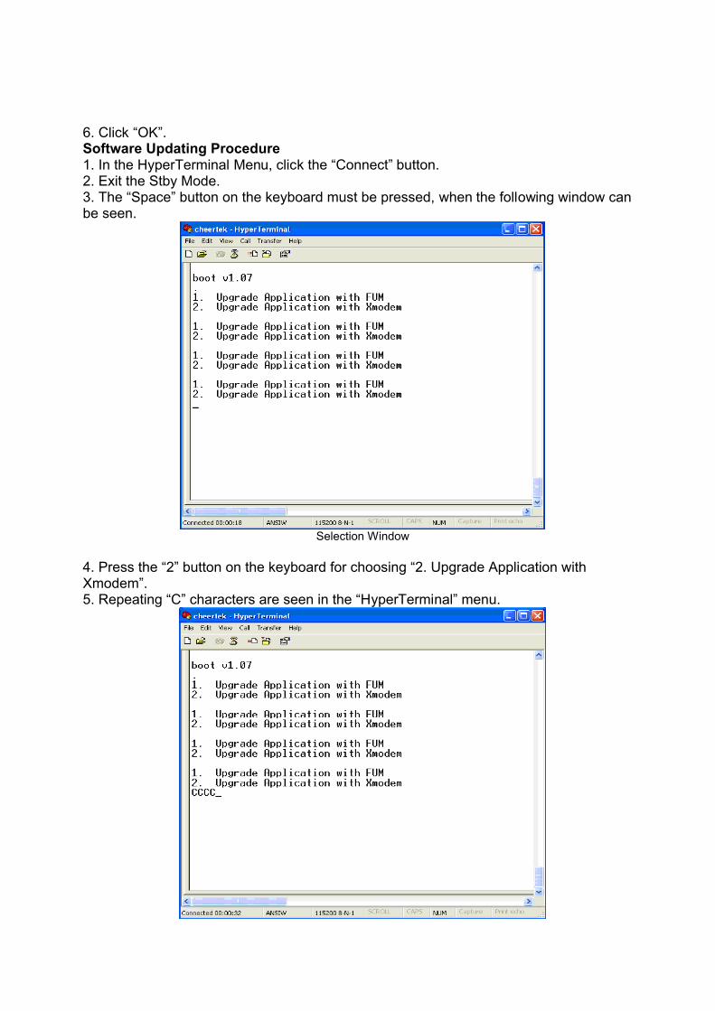
6. Click “OK”.Software Updating Procedure1. In the HyperTerminal Menu, click the “Connect” button. 2. Exit the Stby Mode.3. The “Space” button on the keyboard must be pressed, when the following window can be seen.
Selection Window
4. Press the “2” button on the keyboard for choosing “2. Upgrade Application with Xmodem”.5. Repeating “C” characters are seen in the “HyperTerminal” menu.
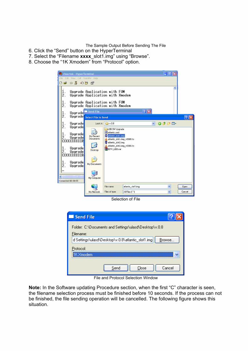
The Sample Output Before Sending The File6. Click the “Send” button on the HyperTerminal7. Select the “Filename xxxx_slot1.img” using “Browse”.8. Choose the “1K Xmodem” from “Protocol” option.
Selection of File
File and Protocol Selection Window
Note: In the Software updating Procedure section, when the first “C” character is seen, the filename selection process must be finished before 10 seconds. If the process can not be finished, the file sending operation will be cancelled. The following figure shows this situation.
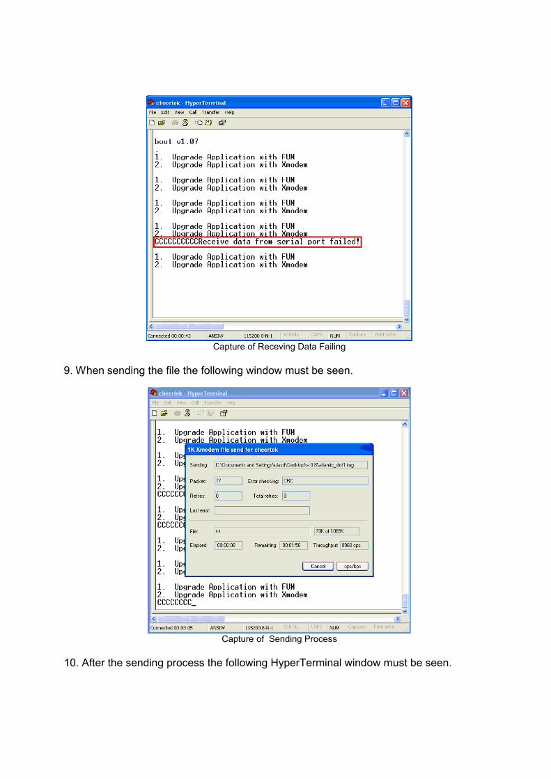
Capture of Receving Data Failing
9. When sending the file the following window must be seen.
Capture of Sending Process
10. After the sending process the following HyperTerminal window must be seen.
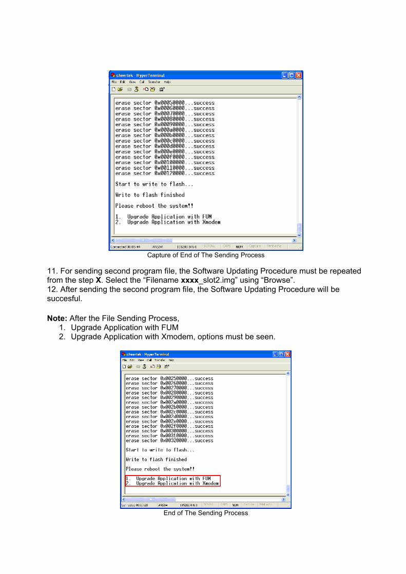
Capture of End of The Sending Process
11. For sending second program file, the Software Updating Procedure must be repeated from the step X. Select the “Filename xxxx_slot2.img” using “Browse”. 12. After sending the second program file, the Software Updating Procedure will be succesful.
Note: After the File Sending Process, 1. Upgrade Application with FUM2. Upgrade Application with Xmodem, options must be seen.
End of The Sending Process
Checking Of The New Software 1. Turn off and on the TV.2. Enter the “Setup” submenu in the “DTV Menu”.3. Choose the “Configuration” option.4. For controlling new software, check the “Receiver Upgrade” option.
16.4 17MB37 Digital Software Update From USBSoftware upgrade is possible via USB disk by folowing the steps below.
1. Copy the bin file, including higher version than the software loaded in flash, into the USB flash memory root directory. This file should be named up.bin.
2. Insert the USB disk.3. Digital module performs version and CRC check. If version and CRC check is
successful, then a message prompt appears to notify user about new version. If the user confirms loading of new version, upgrade.bin file is written into flash unused slot.
4. Digital module disables the previous software in the flash and then a system reset is performed.
5. After the reset, digital module starts with new software.
Revert operation:
With revert operation, it is possible to downgrade the software.Revert operation is very similar to upgrade process. In the revert operation, file name should be f_up.bin. Also user confirmation is not asked.
1. Copy the bin file into the USB flash memory root directory. This file should be named force_upgrade.bin.
2. Insert the USB disk.3. A lower version than the software in flash can be loaded with revert operation.
Digital module performs only CRC check. If CRC check is successful, then force_upgrade.bin file is written into flash unused slot.
4. Digital module disables the previous software in the flash.5. A message prompt is displayed to notify user about end of revert process. 6. Power off/on is required to start digital module with the new software.
For controlling new software, check the “Receiver Upgrade” option.
MST6Wx7
HDMI_1 HDMI_2
DD
C
TMD
S D
ATA
/CLK
HDMI1TMDS DATA/CLOCK 2
TMD
S D
ATA
/CLK
DD
C
HDMI1
HDMI2
THOMSON DTT75430
LGTDTC-GXX1D
4 Layer PCB
DVB-T COFDMDEMOD.STV0362
74HCT4053I2C & AGC SWITCH
I2C LEVEL SHIFTER CIRCUIT
I2CI2C_5V
I2C_TUN_DVB
SAWK9656M
SAWK3958M
VIF_TUNER
SIF_TUNER
MPEG4 DECODER
STi7101
BUFFERS74LCX244
4xDDR116Mx16
CI_BUFFERS
2xFLASHNOR 64Mbit (common)
NAND 2Gbit (w/ethernet)TS_CI
14.3181MHzXTAL
LVDSCONNECTOR
PANEL VCC SW
PANEL_ VCC_ ON/OFF
PANEL_VCC
PANEL SUPPLY
SCA
RT
SC1 CVBSSC1 RGB/FB
SC1 AUD_IN
SC1_CVBS_OUT
SC1_AUD_OUT
YPbPr
YPbP
r
VGA
DD
C
VESTEL ELECTRONICS R&D GROUP
17MB37 BLOCK DIAGRAM
DATE:03.03.2009
DRAWN BY: SADIK ŞEHİT
“”V
GA
/YP
bPr
AU
DIO
L/RFAV_Video/AudioSVHS
I2C
2/U
AR
T
TRANSISTORSWITCH
ON
/OFF
SCL/SDA
SCL/SDA2
EEPROM24C32
Y/C
CVB
S
AUD
IO L
/R
LINE OUT
LIN
E O
UT
L/R
HPAMPLIFIERTDA1308T
HP OUT L/R
AUDIO AMP.PT2333 or MP1720
2 x 2.5W
POP NOISE CIRCUIT
DE
TAC
HE
D H
P
MU
TE
MAIN SPEAKER OUT L/R
Mai
n S
peak
er 4
R
RESET ICMAX809LTR
StBy M TV/AV +P -P +V -V
KEYBOARDI/O PORTS
LED1LED2
DDC_WPPANEL_VCC_ON/OFF
POWER ON/OFFSCART1 PIN8
MPEG DECODER IRQPROTECTION
NVM_WP
I/O PORTS
POWERMODULE
BACKLIGHT_ON/OFF
BACKLIGHT_DIMMING
POWER_ON/OFF
+24V+12V
+5V_STBY
+5V
+3V3_STBY
+3V3I/O
PO
RTS
+3V3_STBY
+1V2_STBY+2V6
+3V3
+5V
+12V
1MB Serial Flash
DVB-C QAMDEMOD.STV0297
ETHERNET PHYSTE101P
RJ45
UARTSPDIF
YPbPr
TS_T
TS_CI
TS_C
ANALOG IF
DIG
ITA
L IF
I2C RF AGC
I2C_5V
RF_AGC_A
RF_AGC_DVB
FSA3157IF AGC
SWITCHIF AGC
IF AGC_C
IF AGC_T
EDIDE2PROM
24C02
EDIDE2PROM
24C02
DVD Connector
+12VDVD Power Connector
DVD
Y/C
_IN
DVD
AU
DIO
_IN
DVD
_SEN
SE
IR
IR ON/OFF
2MB SD RAM
PI5V330RGB Switch
IDTV
_YPb
Pr/S
OY
IDTV
/YPb
Pr_S
W
This Block does not exist, unless PCB has enough
space
USB HUBUSB2503
19 BLOCK DIAGRAMS
19.1 General Block Diagram
10V10u
C363
21
10V10u
C361
21
10V10u C3602
1
10kR505
21 IF_AGC_DVB
R12747R
21
47RR126
21
C134100n 10V
2
1
10V100n
C132
21
10V100n
C131
21
1kR624
21
50V47p C5862
1
RF_AGC
1N4148
D12121
12kR111
21
BC848BQ116
3
2
1
47RR125
21
56RR680
21
5V_TUN
ADDRESS_SEL_TUNER
5V_TUN
ANALOG_IF
5V_TUN
ADDRESS_SEL_TUNER
33V_TUNER
5V_TUN
FDN336P
Q102
3
2
1
BC848BQ115
3
2
1
4R7R482
21
50V1u C532 2
1
ANT_CTRL
ANALOG_IF
4k7
R252
21
1k
R623
21
MST6WB7GQ-3U138
73
72
62
63
64
65
66
67
68
69
70
71 GND_RXV
VIFP
VIFM
SIFM
SIFP
GND_RXS
AVDD_RXS
VR12
VR27
AVDD_MPLL
AVDD_RXV
TAGC
4
17mb37
SADIK SEHIT
ANALOG IF 181
14-10-2009_09:09
87654321
A
B
C
D
E
F
AX M
1 2 3 4 5 6 7 8
A
B
C
D
E
F
OF:
A3PROJECT NAME :VESTELSCH NAME :
DRAWN BY :
SHEET:
K9656M
Z101
41
53
2 IN2GND
OUT2
IN1 OUT1
SIF_CTL
SIFP
SIFM
SIFP
SIFM
SCL_TUNER
SDA_TUNER
SCL_TUNER
33V_TUNER
SDA_TUNER
T_AGC
T_AGC
SCL_TUN
SCL_TUN
SDA_TUN
SCL_TUNER
SDA_TUNER
SDA_TUN
5V_VCC
10V100n
C128
21
22kR595
21
DIGITAL_IF+
DIGITAL_IF-
2R1
TH101
21
16V47u C520
2
1
33V_TUNER
3V3_VCC
BF799Q144
3
2
1
10R
R384
21
1k2R483
21
16V10n
C545
21
C135
100n
10V
2 1
5V_TUN
R408
1k
21
S1052 1330R
R46021
5V_TUN
3V3_VCC
SCL_TUN_DVB
SDASDA_TUN_DVB
5V_TUN
BSN20
Q140
3
2
1
22k
R594
21
5V_TUN
16V10n
C547
21
1kR622
21
R504
10k
21
VIFM
VIFPANALOG_IF
680R
R735
21
IF_AGC_DVB_IN
IF_AGC_DVB_IN
IF_AGC_DVB_IN
C136100n
10V
2
1
10V10u C3592
1
5V_TUN
5V_TUN
R501
10k
21
5V_TUN
5V_VCC
RF_AGC_A
RF_AGC_A
6k8
R473
21
6k8
R474
21
3k3
R231
21
BA782
D1452 1
16V47u C448
2
1
10V10u
C467
21
10V100n C5102
1
50V220p C5972
1
16V47u C600
2
1
330R
F15921
330R
F18421
330R
F18521
330R
F18621
100kR209
21
100k
R210
21
RF_AGC
L114
1u
21
1u
L11121
1u
L101
21
10kR503
21
TP151
1
IDTV_SW
6V3220u C6112
1
3V3_STBY330R
F18721
8V_VCC
LM1117U123
4
3 2
1
GND
OUTIN
VOUT
TU101
DTOS403LH172A
11
10
9
8
7
6
5
4
3
2
1BA
RF_AGC
SAS
SCL
SDA
AIF_OUT
+5V
IF_AGC
VT
IFOUT+
IFOUT-
TU102
TDTC-G101D
12
11
10
9
8
7
6
5
4
3
2
1ANT_PWR
B1
RF_AGC
SCL
SDA
B2
NC
AS
IF_AGC
DIF2
DIF1
AIF
4k7R254
21
74HCT4053U115
1615141312111098
7654321 2Y1
2Y03Y13Z3Y0EVEEGND S3
S2S1
1Y01Y11Z2Z
VCC
16V10n
C546
21
50V47p C5872
1
2u2
L104
21
VIFM
VIFP
50V
100p
C620 2
110V220n C636
4k7R253
21
K3958M
Z102
41
5
3
2 IN2GND
OUT2
IN1 OUT1
10V
100n
C130 2
110V
10u
C364 2
1
10V100n
C129
21
330R
F11621
OVER_CUR_DETECT 330R
F2342 1
S10421
TUNER_PIN11
TUNER_PIN10
1u
L116
21
50V
47p
C626 2
1
RF_AGC
SCLRF_AGC_DVB
10V100n C137
2
1
10kR502
21
220RR1300
6V3220u C1158
S30821
R38220R
50V
2p2
C1029
50V1n
C913
C914
1n 50V
TUNER_PIN11
TUNER_PIN10
TUNER_PIN11
TUNER_PIN10
ACT_ANT
N.C.
OPTIONAL COIL
ACT_ANT
ACTIVE ANTENNA
ACT_ANT
N.C.
WARNING!!! This part must be close to chip
AGC AND I2C SWITCH PART
Near Tunersupply pin
WARNING!!! This part must be close to chip
This part must be placed near the tuner
TUNER SUPPLY OPSION
!!!En az 1.8 cm2 altta ve üstte soðutma alaný býrakýlmalý.
NEAR THE TUNER
V-1 e gecerken yapilan updateler
Video SAW filitre cikislari caprazlandý
N.C.
330R
1K
Samsung/Thomson
LG
WARNING!!! Saw filter outputs must be close the chip
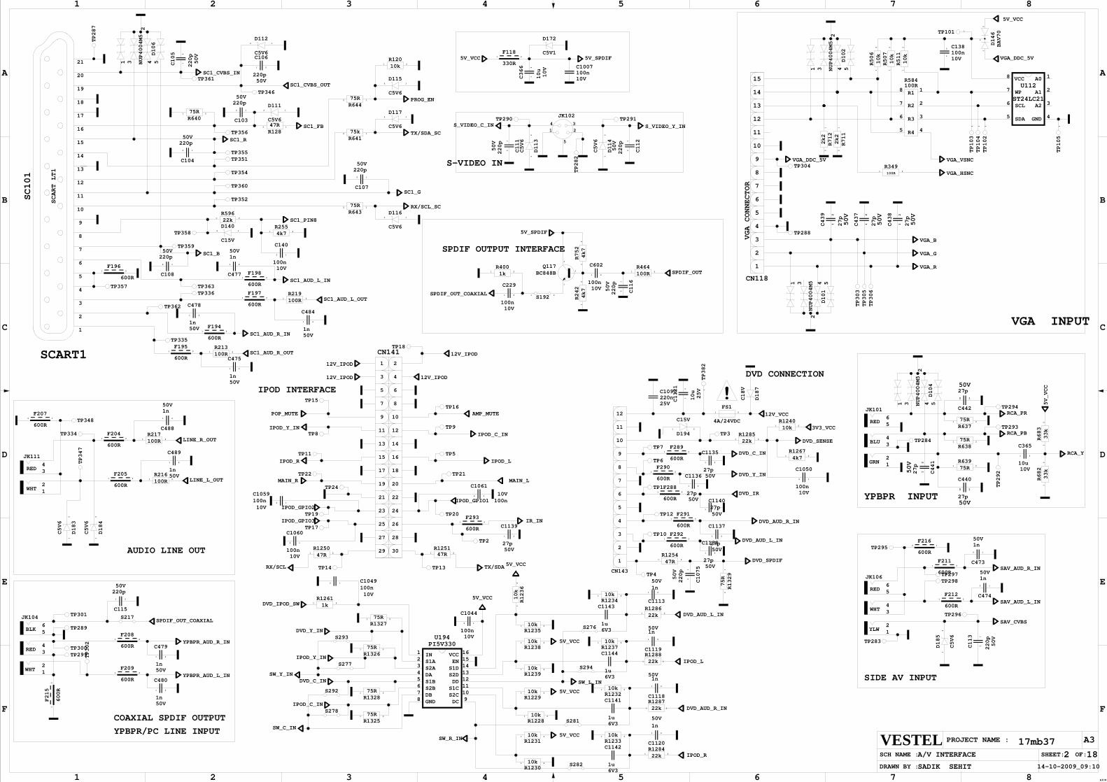
D185
C5V6
21
R584100R
8
7
6
5 4
3
2
1
R2
R3
R1
R4
YPBPR_AUD_L_IN
R349100R
21
D117
C5V6
2 1
R682
33k
21
R64075R 21
C112
220p
50V
21
D114
C5V6
21
C480
1n 50V
21
C479
1n 50V
21
C478
1n 50V
21
C103
220p 50V
2 1
75RR638
21
JK102
5
4 3
21
10k
R506
21
VGA_G
VGA_R
50V
27p
C438 2
1
VGA_B
2k2
R712
21
50V
27p
C439 2
1
10V100n C1382
1
LINE_R_OUT
50V1n
C489
21
17mb37
SADIK SEHIT
A/V INTERFACE 18214-10-2009_09:10
87654321
A
B
C
D
E
F
AX M
1 2 3 4 5 6 7 8
A
B
C
D
E
F
OF:
A3PROJECT NAME :VESTELSCH NAME :
DRAWN BY :
SHEET:
C5V6
D1152 1
10kR120
21
SC1_AUD_R_OUT
75RR644
2 1
JK111
43
21WHT
RED
600R
F20421
F205
600R
21
TP18
NUP4004M5
D106
543
2
1
F207
600R
2 1
LINE_L_OUT
C5V6
D183
21
VGA_DDC_5V
TP102
1
TP104
1
TP103
1
10k
R507
21
10k
R511
21NUP4004M5
D102
543
2
1
2k2
R711
21
BAV70
D146
3
21
VGA_DDC_5V
CN118
15
14
13
12
11
10
9
8
7
6
5
4
3
2
1
NUP4004M5
D104
543
2
1
NUP4004M5
D101
543
2
1
50V1n
C473
2 1
TP105
1
100RR216
21
R64175k2 1
SC1_AUD_L_OUT
50V220p
C106
21
SC1_CVBS_OUT
C107
220p 50V
2 1
4k7R255
21
22kR596
21
SC1_PIN8
50V1n
C475
21
D112
C5V6
2 1
100RR217
21
50V1n
C488
21
TP348
C5V6
D113
21
50V
220p
C111
21
SPDIF_OUT_COAXIAL
TP334
50V
220p
C105 2
1
47RR128
2 1
C5V6
D184
21
U194PI5V330
12345678
161514131211109DC
S2CS1CDD
S2DS1DEN
VCC
GNDDBS2BS1BDAS2AS1AIN
F208
600R
21
600R
F21121
R123910k 21
SC101
21
20
19
18
17
16
15
14
13
12
11
10
9
8
7
6
5
4
3
2
1
SCART LT1
F196
600R
21
BC848BQ117
3
2
1
5V_VCC
600R
F20921
600R
F19821
TP15
SW_L_IN
S_VIDEO_C_IN S_VIDEO_Y_IN
SC1_CVBS_IN
SC1_G
50V
27p
C437 2
1
50V
27p
C4412
1
C440
27p 50V
2 1
S276
RCA_Y
SC1_R50V220p
C104
2 1
SC1_B
SC1_AUD_L_INC477
1n 50V
21
SC1_AUD_R_IN600R
F19421
SC1_FB
C115
220p 50V
21 R123410k 21
6V31u
C1143
5V_VCC
10V100n
C1044
2 1
600R
F215
21
TP16
50V1n
C474
2 1
F212
600R
21
50V
220p
C113
21
SW_R_IN
F216
600R
2 1
SAV_CVBS
5V_VCC
33k
R683
21
C442
27p 50V
2 1
RCA_PR
RCA_PBR63775R 21
R63975R
21
TP347
R123010k 21
D111
C5V6
2 1
C5V6
D1162 1
TX/SDA_SC
RX/SCL_SC
10V10u
C365
21
F197
600R
21
600R
F19521
C15V
D1402 1
5V_VCCR123110k 21
SAV_AUD_L_IN
SAV_AUD_R_IN
75RR643
2 1
50V220p
C108
2 1
10V100n
C140
2 1
TP101 1
5V_SPDIF
10V
10u
C366 2
1
C116
220p
50V
21
VGA_HSNC
VGA_VSNC
JK106
65
43
21YLW
WHT
RED
YPBPR_AUD_R_IN
JK104
2
4
65
3
1
BLK
RED
WHT
JK101
2
4
65
3
1
RED
BLU
GRN
SPDIF_OUT100RR464
21
100RR213
21
100RR219
21
C484
1n 50V
21
SPDIF_OUT_COAXIAL 4k7
R242
21
5V_SPDIF
330R
F118215V_VCC
10V100n
C602
21
10V100n
C229
21
1kR400
21
PROG_EN ST24LC21
U112
8
7
6
5 4
3
2
1A0
A1
A2
GNDSDA
SCL
WP
VCC
4k7
R752
21
S19221
TP8TP9
TP11 TP5
10kR1228
21
12V_IPOD
12V_IPOD
CN141
3029
2827
2625
2423
2221
2019
1817
1615
1413
1211
109
87
65
43
21
12V_IPOD 12V_IPOD
AMP_MUTE
C1090220n 25V
50V27p
C1138
21
50V27p
C1136
21
600R
F29221
F291
600R
21
C1075
220p
50V
21
R125447R
21
10V100n
C1050
2 1
22kR1285
21
F290
600R
21
600R
F28821
C1121
10u
25V2
1
C15V
D19421
R124010k
21
3V3_VCC
12V_VCC
FS1
4A/24VDC
21
DVD_AUD_R_IN
DVD_AUD_L_IN
TP21
C1135
27p 50V
21
C114027p 50V
21
DVD_SPDIF
75R
R1329
21
50V27p
C1137
21
DVD_C_IN
DVD_Y_INTP22
DVD_IR
DVD_SENSE
4k7R1267
21
600R
F28921
CN143
12
11
10
9
8
7
6
5
4
3
2
1
TP382
1
D187
C18V
POP_MUTE
IPOD_Y_INIPOD_C_IN
TP24
TP19
IPOD_GPIO110V100n C1059
2 1
C1060
100n 10V
2 1
IPOD_GPIO2
IPOD_GPIO3
IPOD_R IPOD_L
R125047R
21
RX/SCL TX/SDA
47RR1251
21
C1061
100n 10V2 1
50V27p
C1139
21
IR_INF293
600R
21
MAIN_R MAIN_L
10kR1229
21 5V_VCC
R123810k 21
10kR1235
21
10k
R1236
21
5V_VCC
C1049100n 10V
2 1
C1142
1u 6V3
22kR1286
21 DVD_AUD_L_IN
C1113
1n 50V
21
R128422k
21 IPOD_R
50V
1n
C1120
21
10kR1233
21
22kR1287
21 DVD_AUD_R_IN
TP17
TP14 TP13
TP2
TP20
TP4
TP10
TP12
TP1
TP6
TP7
TP3
R123210k 21
R128822k 21 IPOD_L
C1118
1n 50V
21
50V1n
C1119
21
10kR1237
21
S278
S292
75RR1325
21
IPOD_C_IN
DVD_C_IN
R132875R 21
SW_C_IN
S277
S293
SW_Y_IN
R132675R 21
IPOD_Y_IN
DVD_Y_IN
5V_VCC
75RR1327
21
DVD_IPOD_SW 1kR1261
21
C1144
1u 6V3
6V31u
C1141
S282
S281
S294
S217
C5V1
D172
10V100n C1007
TP292
TP284
TP294
TP293
TP283
TP296
TP298TP297
TP282
TP291TP290
TP295
TP299
TP289
TP301
TP300
TP302
TP305
TP306
TP303
TP288
TP304
TP287
TP361
TP346
TP356
TP355TP351
TP354
TP360
TP352
TP358
TP359
TP363TP357TP336
TP362
TP335
AUDIO LINE OUT
IPOD INTERFACE !DVD CONNECTION
VGA CONNECTOR
SCART1
VGA INPUT
YPBPR INPUT
S-VIDEO IN
COAXIAL SPDIF OUTPUT
YPBPR/PC LINE INPUT
SPDIF OUTPUT INTERFACE
SIDE AV INPUT
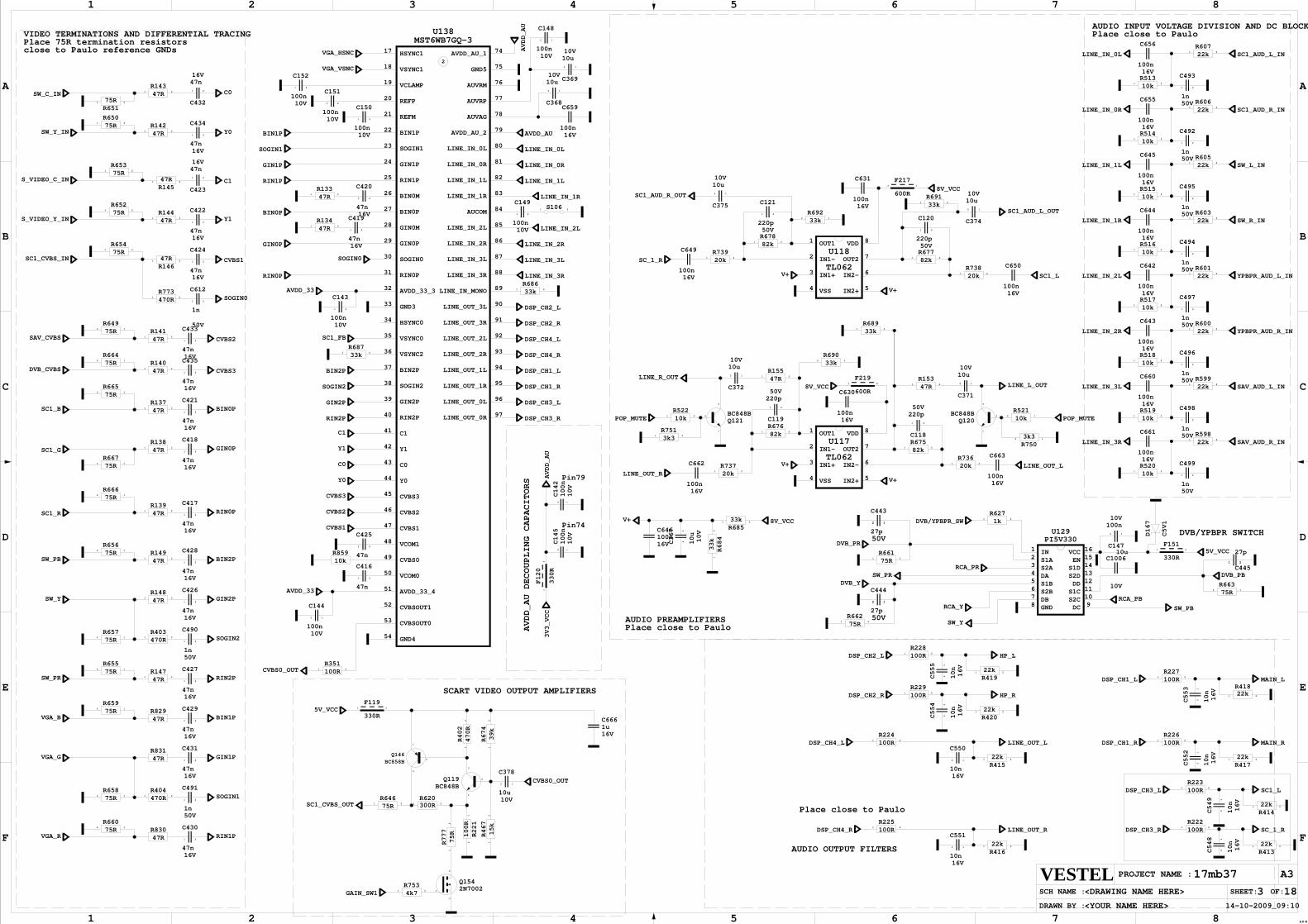
C662
100n 16V
17mb37
183
87654321
A
B
C
D
E
F
AX M
1 2 3 4 5 6 7 8
A
B
C
D
E
F
OF:
A3PROJECT NAME :VESTELSCH NAME :
DRAWN BY :
SHEET:
14-10-2009_09:10
<DRAWING NAME HERE>
<YOUR NAME HERE>
GAIN_SW1
SOGIN0
SOGIN0
DSP_CH2_L
DSP_CH2_R
C494
1n 50V
21
16V100n
C650
8V_VCC
F219
600R
21
SC_1_R 20kR739
21
16V100n
C649
SC1_AUD_R_OUT
SC1_AUD_L_OUT
R73820k
21
SC1_L
10V10u
C374
2 1
V+
V+
V+
R73720k
21
POP_MUTEBC848BQ121
3
2
1
LINE_R_OUT
LINE_OUT_R
16V100n
C663
POP_MUTE
47RR153
21 LINE_L_OUT
20kR736
21
LINE_OUT_LV+
10V10u
C369
2 1
R66775R
2 1
R60722k
21
10kR520
21
10kR519
21
R51810k
21
R51710k
21
R51610k
21
10kR515
21
R51410k
21
R51310k
21
R66375R
2 1
C445
27p
21
10V
100n
C145
2 1
330R
F120
21
VGA_G
VGA_B
C429
47n 16V
21
C430
47n 16V
21
75RR658
2 1
75RR659
2 1
50V1n
C491
21
16V47n
C431
21
75RR660
2 1
SW_PR RIN2P
R65575R
2 1
C426
47n 16V
21
C490
1n 50V
21
R65675R
2 1
R65775R
2 1
R403470R
21
47RR147
21
16V47n
C427
21
R14847R
21
47RR149
21
16V47n
C428
21
75RR654
21
C1
R65375R
21
47RR145
21S_VIDEO_C_IN
R14447R
21
75RR650
21
S106 21
R41922k 21
22kR420
21
16V
10n
C554
21
C555
10n
16V
21
C553
10n
16V
21
16V10n
C550
2 1
33k
R684
21
470R
R402
21
SC1_CVBS_OUT
16V100n
C659
16V100n
C660
16V100n
C661
C498
1n 50V
21
C499
1n 50V
21
50V1n
C492
21
50V1n
C493
21
50V1n
C495
21
50V1n
C496
21
50V1n
C497
21
16V100n
C642
16V100n
C643
16V100n
C645
16V100n
C644
16V100n
C656
16V100n
C655
SW_L_IN
SC1_AUD_R_IN
SW_R_IN
10V100n
C148
2 1
10V100n
C149
21
100RR351
21CVBS0_OUT
10V100n
C147
2 1
5V_VCC
C548
10n
16V
21
16V
10n
C549
21
16V
10n
C552
21
R41622k 21
R41822k 21
22kR417
21
22kR414
21
R41322k 21
22kR415
21
SC1_AUD_L_IN
YPBPR_AUD_L_IN
YPBPR_AUD_R_IN
33kR685
21V+AVDD_AU
BC848BQ119
3
2
1
C551
10n 16V
2 1
47RR134
21
R674
39k
21
R467
15k
21
C421
47n 16V
21
R13347R
21
R13747R
21
47RR138
21
C417
47n 16V
21
R13947R
21
R14047R
21
AVDD_AU
LINE_IN_0R
LINE_IN_0L
LINE_IN_0R
LINE_IN_0L
LINE_IN_1L
LINE_IN_1R
LINE_IN_1L
LINE_IN_1RLINE_IN_2L
LINE_IN_3R LINE_IN_2L
LINE_IN_3L
LINE_IN_2R
LINE_IN_3R
LINE_IN_3L
R65175R 21
R14247R
21 Y0
C0SW_C_IN 47RR143
21
Y1S_VIDEO_Y_IN
16V47n
C434
21
16V47n
C432
21
16V47n
C423
21
SC1_CVBS_IN
16V47n
C435
21
16V47n
C433
2147RR141
21
C425
47n
21
75RR664
2 1
DVB_CVBS
CVBS2
CVBS3
75RR652
21 C422
47n 16V
21
C424
47n 16V
21
R64975R
2 1
10kR859
CVBS1
CVBS2
CVBS3
RIN0P
BIN0P
GIN0P
SC1_B
SC1_G
16V47n
C418
21
75RR666
2 1
SC1_R
C419
47n 16V
21
RIN0P
GIN0P
BIN2P
GIN2P
SOGIN2
SW_PB
SW_Y RCA_PBRCA_Y
SW_Y
1kR627
21
DVB/YPBPR_SW
RCA_PRSW_PR
C416
47n
21
Y0
C0
Y1
C1
RIN2P
GIN2P
SOGIN2
BIN2P
BIN0P
SOGIN1
GIN1P
RIN1P
BIN1P 10V100n
C150
2110V100n
C151
21
VGA_VSNC
VGA_HSNC
VGA_R
BIN1P
GIN1P
SOGIN1
RIN1P
PI5V330U129
12345678
161514131211109DC
S2CS1CDD
S2DS1DEN
VCC
GNDDBS2BS1BDAS2AS1AIN
16V47n
C420
21
AVDD_AU
10V100n
C152
21
C143
100n 10V
21
AVDD_33
MST6WB7GQ-3U138
84
83
81
80
79
85
86
78
77
76
87
88
89
75
74
90
91
92
93
94
95
96
97
17
18
19
20
21
22
23
24
25
26
27
28
29
30
31
32
33
34
35
36
37
38
39
40
41
42
43
44
45
46
47
48
49
50
51
52
53
54
82LINE_IN_1L
GND4
CVBSOUT0
CVBSOUT1
AVDD_33_4
VCOM0
CVBS0
VCOM1
CVBS1
CVBS2
CVBS3
Y0
C0
Y1
C1
RIN2P
GIN2P
SOGIN2
BIN2P
VSYNC2
VSYNC0
HSYNC0
GND3
AVDD_33_3
RIN0P
SOGIN0
GIN0P
GIN0M
BIN0P
BIN0M
RIN1P
GIN1P
SOGIN1
BIN1P
REFM
REFP
VCLAMP
VSYNC1
HSYNC1
LINE_OUT_0R
LINE_OUT_0L
LINE_OUT_1R
LINE_OUT_1L
LINE_OUT_2R
LINE_OUT_2L
LINE_OUT_3R
LINE_OUT_3L
AVDD_AU_1
GND5
LINE_IN_MONO
LINE_IN_3R
LINE_IN_3L
AUVRM
AUVRP
AUVAG
LINE_IN_2R
LINE_IN_2L
AVDD_AU_2
LINE_IN_0L
LINE_IN_0R
LINE_IN_1R
AUCOM
2
3V3_VCC
R68633k
21
SAV_CVBS
SAV_AUD_L_IN
SAV_AUD_R_IN
DVB_Y
C443
27p 50V
2 1
75RR662
2150V27p
C444
2 1
R66175R
21
SW_PB
DVB_PB
DVB_PR
22kR598
21
R59922k
21
22kR600
21
R60122k
21
R60322k
21
R60522k
21
22kR606
21
DSP_CH1_L
DSP_CH1_R
DSP_CH1_R
DSP_CH1_L
DSP_CH4_L
DSP_CH4_R
HP_R
HP_LDSP_CH2_L
DSP_CH2_R
DSP_CH4_L
DSP_CH4_R
DSP_CH3_L
DSP_CH3_R
5V_VCC330R
F11921
75RR665
2 1
33kR687
21
SC1_FB
10V100n
C144
2 1
16V100n C646
C368
10u 10V
2 1
SW_Y_IN
C118
220p 50V
21
82kR675
21
Q120BC848B
3
2
1
R68933k
21
82kR676
21
C119
220p 50V
21
33kR690
2 1
R15547R
21
TL062
U1178
7
6
54
3
2
1 OUT1
IN1-
IN1+
VSS IN2+
IN2-
OUT2
VDD
33kR691
21
50V220p
C120
21
82kR677
21
33kR692
2 1
50V220p
C121
21
82kR678
21
U118
TL062
8
7
6
54
3
2
1 OUT1
IN1-
IN1+
VSS IN2+
IN2-
OUT2
VDD
8V_VCC
F217
600R
2 1
8V_VCC
C142
100n
10V
2 1
10V
10u
C367
21
16V1u C666
10V10u
C378
2 1
C375
10u 10V
2 1
10V10u
C372
2 1
C371
10u 10V
2 1
330R
F15121
100RR228
21
100RR229
21
100RR224
21
100RR225
21
100RR223
21
100RR226
21
100RR227
21
LINE_IN_2R
DSP_CH3_L
DSP_CH3_R
CVBS1
AVDD_33
47RR829
47RR831
16V100n
C631
16V100n
C630
100R
R221
21
BC858BQ146
3
2
1
75RR646
21 300RR620
21
CVBS0_OUT
10kR521
2 1
R52210k
21
R14647R 21
R773470R
21
C612
1n
50V
21
47RR830
470RR404
21
75R
R777
21
4k7R753
21 2N7002Q154
3
2
1
3k3R751
21 3k3R750
2 1
MAIN_L
MAIN_R
SC_1_R
SC1_L
LINE_OUT_L
LINE_OUT_R 100RR222
21
10V
10u C1006
C5V1
D167
AUDIO INPUT VOLTAGE DIVISION AND DC BLOCK
DVB/YPBPR SWITCH
Place close to PauloVIDEO TERMINATIONS AND DIFFERENTIAL TRACINGPlace 75R termination resistorsclose to Paulo reference GNDs
Pin79
Pin74AVDD_AU DECOUPLING CAPACITORS
Place close to PauloAUDIO PREAMPLIFIERS
SCART VIDEO OUTPUT AMPLIFIERS
AUDIO OUTPUT FILTERS
Place close to Paulo
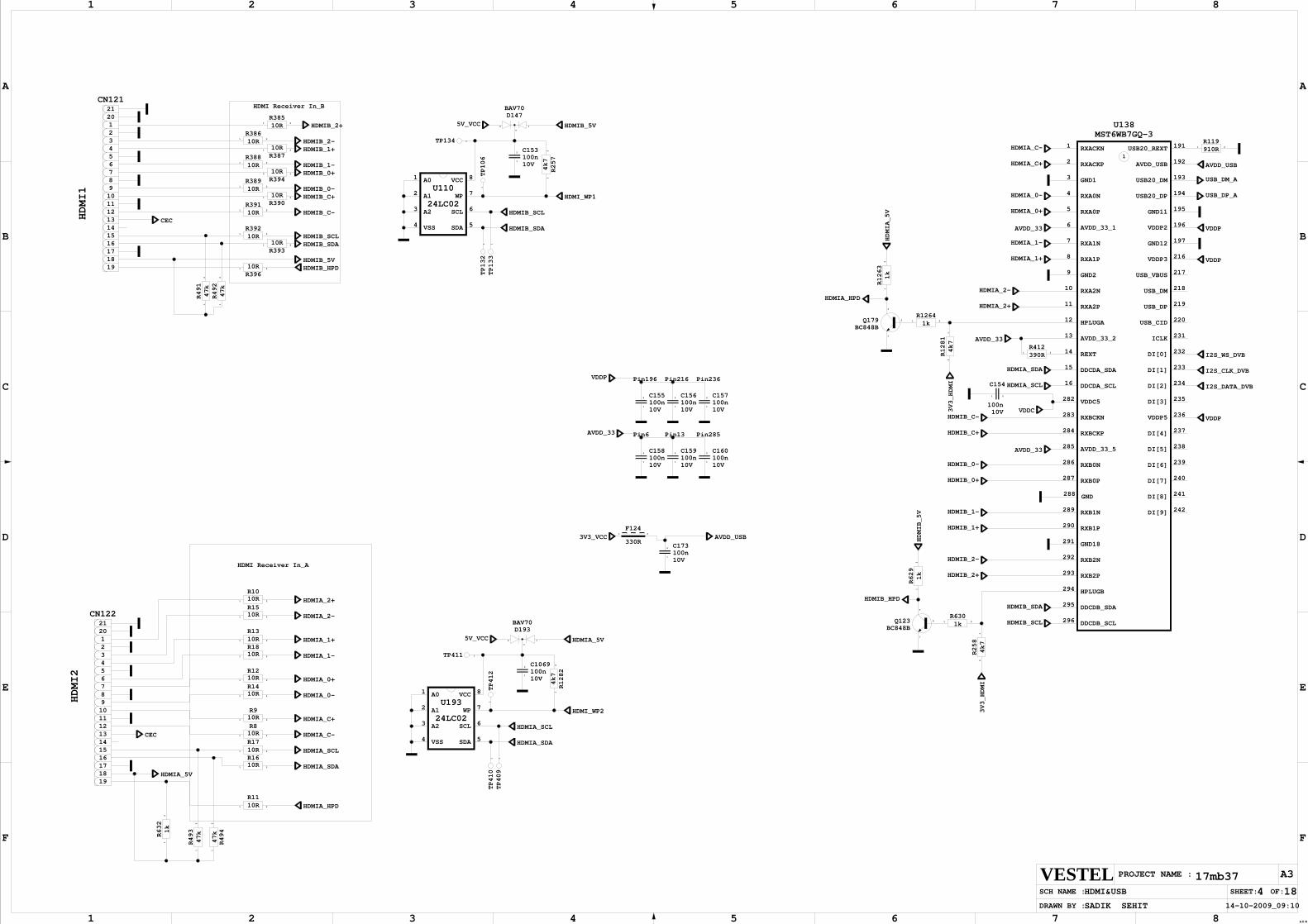
R1010R 21
10RR15
21
R1310R 21
10RR18
21
R1210R 21
10RR14
21
R910R 21
10RR8
21
R1710R 21
10RR16
21
R1110R 21
R1281
4k7
21
1kR1264
21
HDMIA_5V
TP410
1
Q179BC848B
3
2
1
1k
R1263
21
TP412
1
HDMIA_SCL
HDMIA_SDA
HDMIA_5V5V_VCC
BAV70D193
3
2 1
R1282
4k7
21
C1069100n 10V
2
1
U193
24LC02
8
5
6
7
4
3
2
1 A0
A1
A2
VSS
WP
SCL
SDA
VCC
HDMI_WP2
TP409
1
TP411 1
3V3_HDMI
TP134 1
TP133
1
HDMIB_2+
HDMIB_1+
HDMIB_1-
HDMIB_0+
HDMIB_0-
HDMIB_C+
HDMIA_5V
HDMIB_5V
R629
1k
21
R39610R 21
C173100n 10V
2
1
AVDD_USB3V3_VCC
10V100n C1602
1
C159100n 10V
2
1
C157100n 10V
2
1
HDMI_WP1
390RR412
21
AVDD_33
R39110R
21
R38810R
21
HDMIA_1+
CEC
HDMIA_2-
HDMIA_1-
HDMIA_0+
HDMIA_0-
HDMIA_C+
HDMIA_C-
HDMIA_2+
17mb37
SADIK SEHIT
HDMI&USB 18414-10-2009_09:10
87654321
A
B
C
D
E
F
AX M
1 2 3 4 5 6 7 8
A
B
C
D
E
F
OF:
A3PROJECT NAME :VESTELSCH NAME :
DRAWN BY :
SHEET:
24LC02
U1108
5
6
7
4
3
2
1 A0
A1
A2
VSS
WP
SCL
SDA
VCC
R38610R
21
10RR385
21
HDMIB_1+
HDMIB_1-HDMIB_0+10R
R3942 1
10RR387
21
HDMIB_0-HDMIB_C+
R38910R
21
10RR390
21
CN1222120
19181716151413121110987654321
CN1212120
19181716151413121110987654321
VDDC
VDDP
VDDP
VDDP
10V100n C1562
1
VDDP
10V100n
C154
21
AVDD_33
AVDD_33
10V100n C1582
1
C155100n 10V
2
1
10RR392
21
HDMIB_SCL
HDMIB_C-
R39310R 21
10V100n C1532
1
4k7
R257
21
BC848BQ123
3
2
1
HDMIB_SDA
HDMIA_HPD
HDMIA_SCL
HDMIA_SDA
F124
330R
21
910RR119
21
47k
R491
21
47k
R492
21
R632
1k
21 R493
47k
21
R494
47k
21
CEC
AVDD_USB
HDMIA_2+
HDMIA_2-
HDMIA_1+
HDMIA_1-
AVDD_33
HDMIA_0+
HDMIA_0-
HDMIA_C-
HDMIB_C-
HDMIA_C+
HDMIB_HPD
HDMIB_5V
R6301k
21
3V3_HDMI
HDMIB_2-
HDMIA_SDA
HDMIA_SCL
HDMIB_SDA
HDMIB_SCL
HDMIB_2+
HDMIB_2-
HDMIB_HPD
HDMIA_HPD
D147BAV70
3
2 15V_VCC HDMIB_5V
HDMIB_SDA
HDMIB_SCL
TP106
1TP132
1
MST6WB7GQ-3U138
288
191
192
220
232
219
233
218
234
217
235
216
236
197
237
196
238
195
239
194
240
193
241
242
1
2
3
4
5
6
7
8
9
10
11
12
13
14
15
16
282
283
284
285
286
287
289
290
291
292
293
294
295
296
231ICLK
DDCDB_SCL
DDCDB_SDA
HPLUGB
RXB2P
RXB2N
GND18
RXB1P
RXB1N
RXB0P
RXB0N
AVDD_33_5
RXBCKP
RXBCKN
VDDC5
DDCDA_SCL
DDCDA_SDA
REXT
AVDD_33_2
HPLUGA
RXA2P
RXA2N
GND2
RXA1P
RXA1N
AVDD_33_1
RXA0P
RXA0N
GND1
RXACKP
RXACKN
DI[9]
DI[8]
USB20_DM
DI[7]
USB20_DP
DI[6]
GND11
DI[5]
VDDP2
DI[4]
GND12
VDDP5
VDDP3
DI[3]
USB_VBUS
DI[2]
USB_DM
DI[1]
USB_DP
DI[0]
USB_CID
AVDD_USB
USB20_REXT
GND
1
I2S_WS_DVB
I2S_CLK_DVB
I2S_DATA_DVB
4k7
R258
21
USB_DP_A
USB_DM_A
HDMI Receiver In_A
Pin6 Pin13 Pin285
Pin236Pin216Pin196
HDMI2
HDMI1
HDMI Receiver In_B
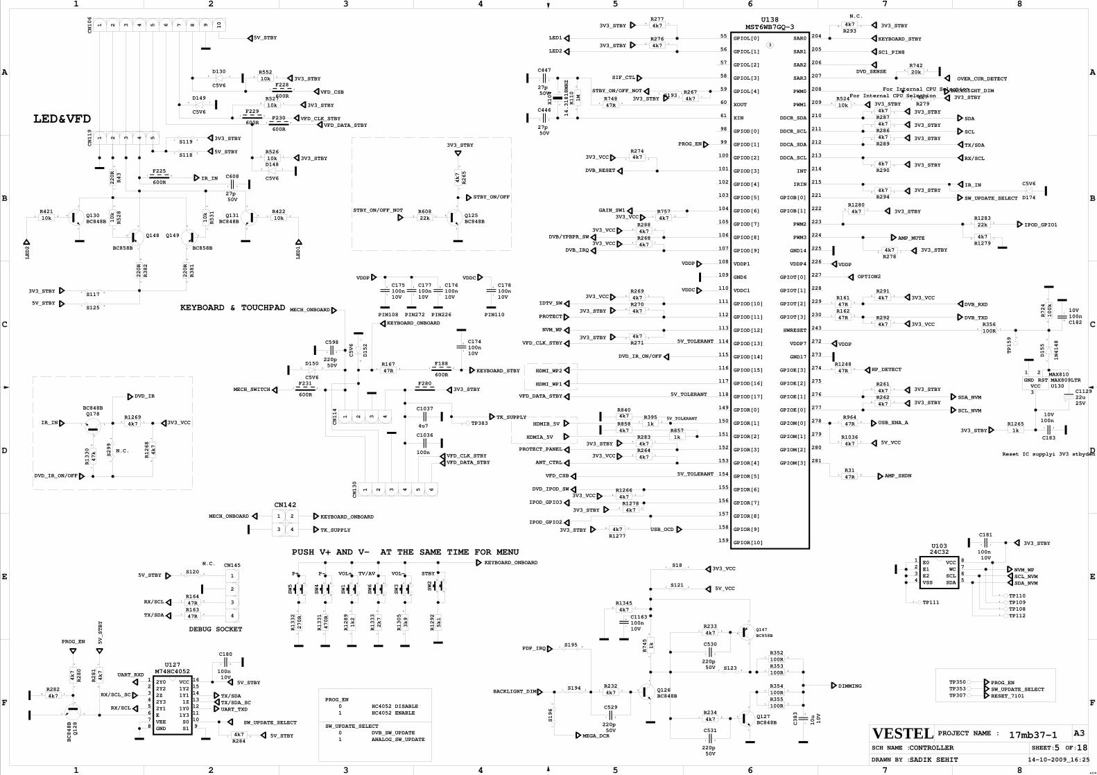
1
R13454k7
2
F280
4u7
C1037
100n
C1036
C5V6
D174
CN145
4
3
2
1
KEYBOARD_ONBOARD
MECH_ONBOARD
DVD_IR_ON/OFF
C1163100n 10V
2
1
HDMI_WP2
TK_SUPPLY
DVD_IPOD_SW R12664k7
2 13V3_VCCIPOD_GPIO3
3V3_STBYR12784k7
2 1
TP3831
CN142
43
21
IPOD_GPIO1
4k7R1280
2 1
3V3_STBYR128322k
21
R12794k72 1
MECH_ONBOARD KEYBOARD_ONBOARDIPOD_GPIO2
3V3_STBYR12774k72 1
TK_SUPPLY
3V3_STBYR12651k
C112922u 25V
HP_DETECTR124847R
21
AMP_SHDN
IR_IN
R1330
47k
21
3V3_VCC
Q178BC848B
3
2
1
S299
21
DVD_IR
DVD_IR_ON/OFF
4k7
R1268
21
4k7R1269
2 1
5k1
R1292
R1332
270R
21
R1331
470R
21
R1289
1k2
21
R1333
2k7
21
R1305
3k9
21
SW5
43
21
SW1
43
21
SW6
43
21
SW3
43
21
SW4
43
21
KEYBOARD_ONBOARD
SW2
43
21
R3147R
21VFD_CSB
D130
C5V6
2 1
R16147R
21
R16247R
21
C180
100n 10V
21
S120 21
5V_STBYR2844k7 21
3V3_STBYR2834k7
2 1
4k7R282
2 1
4k7R277
2 1
R2764k7
2 1
3V3_STBY
C178100n 10V
2
1
C176100n 10V
2
1
C177100n 10V
2
1
10V100n C1752
1
MAX809LTRU130
3
21
GND RSTVCC
TP1081
TP1091
10V100n
C181
2 1
TP1101
TP1121
24C32U103
78
654
321 E0
E1E2VSS SDA
SCL
VCCWC
10k
R528
21
BC858B
Q148
3
2
1
BC848BQ130
3
2
1
R382
220R
21
SCL_NVM
R60822k
2 1
BC848BQ125
3
2
1
SDA_NVM
NVM_WP
TP1111
100RR356
2 1
100k
R724
21
10V100n C182
2
1
10V100n
C183
21
14.31818MHZ
X104 2
1
1M
R110
21
50V27p
C447
21
VDDP
VDDP
VDDP
VDDP VDDC
VDDC
LED1
3V3_STBY
3V3_STBY
R2674k7
2 1
3V3_STBY
DVB/YPBPR_SW3V3_VCC
DVB_IRQ
R2684k7
2 13V3_VCC
IDTV_SW
PROTECT
HDMI_WP1
ANT_CTRL
BC848BQ126
3
2
1
BC858BQ147
3
2
1
Q127BC848B
3
2
1
100RR354
21
R355100R
21
10kR524
2 1
KEYBOARD_STBY
SC1_PIN8
SCL
SDA3V3_STBY
3V3_STBY
TX/SDA
4k7R289
2 1
RX/SCL
3V3_VCCR2914k7
2 1
4k7R292
2 1
3V3_VCC
SDA_NVM
SCL_NVM
SIF_CTL
LED2
BACKLIGHT_DIM
DVB_TXD
DVB_RXD
4k7R294
2 1
HDMIB_5V
HDMIA_5V
STBY_ON/OFF_NOT
4k7R286
2 1
3V3_STBY
3V3_STBY
3V3_STBY4k7R287
2 1
R2904k72 1 3V3_STBY
R2884k7
2 1
5V_STBY
BC848B
Q128
3
2
1
R280
4k7
21
17mb37-1
SADIK SEHIT
CONTROLLER 18514-10-2009_16:25
87654321
A
B
C
D
E
F
AX M
1 2 3 4 5 6 7 8
A
B
C
D
E
F
OF:
A3PROJECT NAME :VESTELSCH NAME :
DRAWN BY :
SHEET:
U127M74HC4052
1615141312111098
7654321 2Y0
2Y22Z2Y32Y1EVEEGND S1
S01Y31Y01Z1Y11Y2VCC
PROG_EN 5V_STBY
R281
4k7
21
R2614k7
2 1 3V3_STBY
SW_UPDATE_SELECT
5V_STBY
5V_STBY
TX/SDAR16347R
21
RX/SCL 47RR164
21
AMP_MUTE
RX/SCL_SC
RX/SCL
TX/SDA
S121 21
STBY_ON/OFF
3V3_STBY
10V
10u
C383 2
1
R2934k72 1 3V3_STBY
DVD_SENSE
3V3_VCCR2644k7
2 1
3V3_STBY 4k7R271
2 1
4k7R269
2 1
R2704k7
2 1
3V3_STBY
3V3_VCC
PROTECT_PANEL
IR_IN
100RR352
21
R353100R
2150V
220p
C530
21
4k7R233
21
C5V6
D1482 1
10kR421
21
1k
R745
21
4k7R234
21
50V220p
C531
21
BC858B
Q149
3
2
1
220R
R381
21
10k
R531
21
BC848BQ131
3
2
1
10kR422
21
LED1
R2794k72 1 3V3_STBY
20kR742
2 1
OVER_CUR_DETECT
3V3_STBY
5V_STBY
VFD_CLK_STBYC5V6
D1492 1
3V3_STBY10kR552
2 1
5V_STBY
VFD_DATA_STBY
VFD_CLK_STBY
1kR395
21
TX/SDA_SCUART_TXD
UART_RXD
SW_UPDATE_SELECT
R52610k
2 1
C446
27p 50V
21
R2784k72 1
STBY_ON/OFF_NOT
S11921
S19321
DVB_RESET
GAIN_SW1
4k7R757
213V3_VCC
50V220p
C529
21
PROG_EN
4k7R274
213V3_VCC
PDP_IRQ
S123 21
BACKLIGHT_DIMDIMMING
MEGA_DCR
S12521
CN106
10987654321
LED2
MECH_SWITCH
3V3_STBY
4k7
R265
21
3V3_STBYS117
21
C608
27p 50V
21
S11821
3V3_STBY
3V3_STBY
600R
F22521
VFD_CSB
VFD_DATA_STBY
3V3_STBYR52710k
2 1
600R
F22921
F230
600R
21
F228
600R
21
NVM_WP
5V_VCC
R2624k7
2 1
R74847R
21
IR_IN
KEYBOARD_STBY
1N4148
D155
21
TP159 1
MST6WB7GQ-3U138
213
212
281
279
278
277
276
275
274
273
272
243
230
229
228
227
225
224
223
222
221
215
214
209
208
207
206
205
20455
56
57
58
59
60
61
98
99
100
101
102
103
104
105
106
107
108
109
110
111
112
113
114
115
116
117
118
149
150
151
152
153
154
155
156
157
158
159
226
280
210
211DDCR_SCL
DDCR_SDA
GPIOM[2]
VDDP4
GPIOR[10]
GPIOR[9]
GPIOR[8]
GPIOR[7]
GPIOR[6]
GPIOR[5]
GPIOR[4]
GPIOR[3]
GPIOR[2]
GPIOR[1]
GPIOR[0]
GPIOD[17]
GPIOD[16]
GPIOD[15]
GPIOD[14]
GPIOD[13]
GPIOD[12]
GPIOD[11]
GPIOD[10]
VDDC1
GND6
VDDP1
GPIOD[9]
GPIOD[8]
GPIOD[7]
GPIOD[6]
GPIOD[5]
GPIOD[4]
GPIOD[3]
GPIOD[2]
GPIOD[1]
GPIOD[0]
XIN
XOUT
GPIOL[4]
GPIOL[3]
GPIOL[2]
GPIOL[1]
GPIOL[0] SAR0
SAR1
SAR2
SAR3
PWM0
PWM1
INT
IRIN
GPIOB[0]
GPIOB[1]
PWM2
PWM3
GND14
GPIOT[0]
GPIOT[1]
GPIOT[2]
GPIOT[3]
HWRESET
VDDP7
GND17
GPIOE[3]
GPIOE[2]
GPIOE[1]
GPIOE[0]
GPIOM[0]
GPIOM[1]
GPIOM[3]
DDCA_SDA
DDCA_SCL
3
S195 21
S194 21
S196
21
4k7R232
21
C5V6
D1502150V
220p
C598
21
D152
C5V6
21
R16747R
21
10V100n C1742
1
F188
600R
21
600R
F23121
CN114
4321
3V3_STBY
OPTION2
CN119
54321
S18 21 3V3_VCC
R43
220R
21
CN130
654321
VFD_CLK_STBYVFD_DATA_STBY
4k7R840
1kR8574k7
R858 USB_ENA_A47RR964
21
4k7R1036
2 1 5V_VCC
USB_OCD
PROG_ENTP350
SW_UPDATE_SELECTTP353
RESET_7101TP307
N.C.
STBY
PUSH V+ AND V- AT THE SAME TIME FOR MENU
VOL-TV/AVVOL+P-P+
5V_TOLERANT
5V_TOLERANT
5V_TOLERANT
10
SW_UPDATE_SELECT
PROG_EN
LED&VFD
PIN272 PIN226PIN108 PIN110
HC4052 DISABLEHC4052 ENABLE1
DVB_SW_UPDATEANALOG_SW_UPDATE
N.C.
DEBUG SOCKET
5V_TOLERANT
For Internal CPU SelectionFor Internal CPU Selection
MAX810
0
N.C.
KEYBOARD & TOUCHPAD
Reset IC supplyi 3V3 stbyden alindi
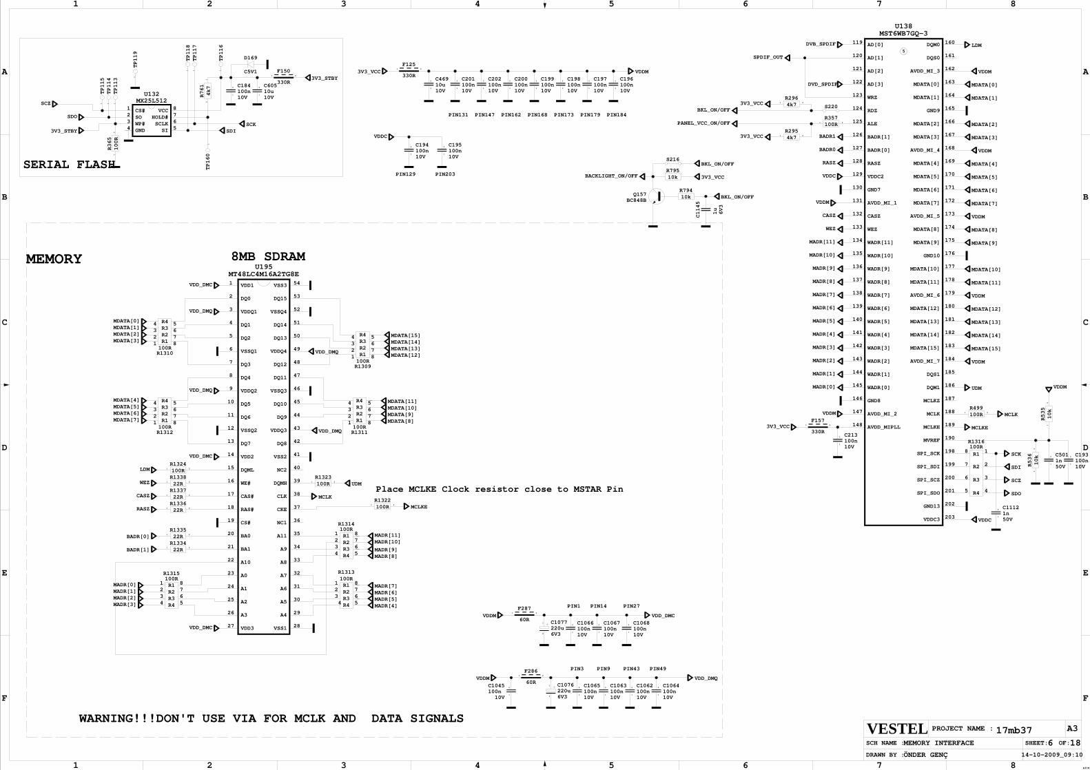
10V100n C10642
1
VDDM
C1045100n 10V
2
1
F286
60R
21
C1063100n 10V
2
1
C1062100n 10V
2
1
C1076220u 6V32
1
10V100n C10652
1
100n 10V
C10672
1
VDDM
F287
60R
21
C1066100n 10V
2
1
C1077220u 6V32
1 C1068100n 10V
2
1
SDO
SCZ
SDI
SCK
50V1n C11122
1
100RR1316
8
7
6
5 4
3
2
1
R2
R3
R1
R4
DVD_SPDIF
6V3
1u
C1145
VDD_DMC
VDD_DMQ
S220
U195MT48LC4M16A2TG8E1
2
3
4
5
6
7
8
9
10
11
12
13
14
15
16
17
18
19
20
21
22
23
24
25
26
27
54
53
52
51
50
49
48
47
46
45
44
43
42
41
40
39
38
37
36
35
34
33
32
31
30
29
28VSS1
A4
A5
A6
A7
A8
A9
A11
NC1
CKE
CLK
DQMH
NC2
VSS2
DQ8
VDDQ3
DQ9
DQ10
VSSQ3
DQ11
DQ12
VDDQ4
DQ13
DQ14
VSSQ4
DQ15
VSS3
VDD3
A3
A2
A1
A0
A10
BA1
BA0
CS#
RAS#
CAS#
WE#
DQML
VDD2
DQ7
VSSQ2
DQ6
DQ5
VDDQ2
DQ4
DQ3
VSSQ1
DQ2
DQ1
VDDQ1
DQ0
VDD1VDD_DMC
VDD_DMQ
R1310100R
87654
321
R4R3R2R1MDATA[3]
MDATA[2]MDATA[1]MDATA[0]
100RR1312
87654
321
R4R3R2R1
VDD_DMQ
DVB_SPDIF
MDATA[6]MDATA[7]
MDATA[4]
MX25L512U132
87654
321 CS#
SOWP#GND SI
SCLKHOLD#VCC
MDATA[5]
VDD_DMC
100RR1324
21LDM
10V100n C1962
1
C197100n 10V
2
1
10V100n C1982
1
C199100n 10V
2
1
10V100n C2002
1
10V100n C2012
1
C202100n 10V
2
1
MDATA[4]
10V100n C1932
1
22RR1338
21WEZ
100RR357
21
22RR1337
21CASZ
22RR1336
21RASZ
R133522R
21
BADR[0]
22RR1334
21
BADR[1]
VDDM
MADR[0]
MCLKE
WEZ
MADR[7]
R1314100R
87654
321
R4R3R2R1
MADR[8]
MADR[10]
MADR[9]
R1315100R
87654
321
R4R3R2R1
MADR[1]MADR[0]
MADR[3]MADR[2]
VDD_DMC
MADR[4]
MADR[6]MADR[5]
MADR[7]
100RR1313
87654
321
R4R3R2R1
MADR[11]
MCLK
MCLKE100RR1322
21
UDMR1323100R
21
VDD_DMQ100RR1311
87654
321
R4R3R2R1
MDATA[11]
MDATA[9]MDATA[10]
100R
R365
21
SDI
17mb37
ÖNDER GENÇ
MEMORY INTERFACE 18614-10-2009_09:10
87654321
A
B
C
D
E
F
AX M
1 2 3 4 5 6 7 8
A
B
C
D
E
F
OF:
A3PROJECT NAME :VESTELSCH NAME :
DRAWN BY :
SHEET:
MDATA[8]
100RR1309
87654
321
R4R3R2R1
SCZ
SDO
MDATA[14]MDATA[15]
MDATA[13]MDATA[12]
VDD_DMQ
MDATA[0]
MDATA[1]
MDATA[2]
MDATA[3]
MDATA[5]
MDATA[6]
MDATA[7]
MDATA[8]
MDATA[9]
MDATA[12]
MDATA[13]
MDATA[14]
MDATA[15]
MADR[2]
MADR[3]
MADR[4]
MADR[5]
MADR[6]
MADR[9]
MADR[8]
RASZ
BADR0
MDATA[10]
SCK
10k
R535
21
R536
10k
21
50V1n C5012
1
MADR[1]
MADR[10]
MADR[11]
VDDM
VDDM
MDATA[11]
MST6WB7GQ-3U138
203
202
201
200
199
190
189
188
187
186
185
184
183
182
181
180
178
177
176
175
174
173
172
171
169
168
167
165
164
163
161
160119
120
121
122
123
124
125
126
127
128
129
130
131
132
133
134
135
136
137
138
139
140
141
142
143
144
145
146
147
148
198
179
170
166
162AVDD_MI_3
MDATA[2]
MDATA[5]
AVDD_MI_6
SPI_SCK
AVDD_MIPLL
AVDD_MI_2
GND8
WADR[0]
WADR[1]
WADR[2]
WADR[3]
WADR[4]
WADR[5]
WADR[6]
WADR[7]
WADR[8]
WADR[9]
WADR[10]
WADR[11]
WEZ
CASZ
AVDD_MI_1
GND7
VDDC2
RASZ
BADR[0]
BADR[1]
ALE
RDZ
WRZ
AD[3]
AD[2]
AD[1]
AD[0] DQM0
DQS0
MDATA[0]
MDATA[1]
GND9
MDATA[3]
AVDD_MI_4
MDATA[4]
MDATA[6]
MDATA[7]
AVDD_MI_5
MDATA[8]
MDATA[9]
GND10
MDATA[10]
MDATA[11]
MDATA[12]
MDATA[13]
MDATA[14]
MDATA[15]
AVDD_MI_7
DQS1
DQM1
MCLKZ
MCLK
MCLKE
MVREF
SPI_SDI
SPI_SCZ
SPI_SDO
GND13
VDDC3
5
VDDC
LDM
UDM
10V100n C2132
1
3V3_VCC
BADR1
VDDC
VDDC
CASZ
VDDM
C194100n 10V
2
1
VDDM
VDDM
VDDM
10V100n C1952
1
F125
330R
21
VDDM3V3_VCC
3V3_STBY
330R
F15721
TP118
1
TP113
1
TP115
1
TP114
1
TP119
1
VDDM
MCLK100RR499
21
BKL_ON/OFF
4k7R295
213V3_VCC
PANEL_VCC_ON/OFF
R2964k7
213V3_VCC
10V10u C4692
1
3V3_STBY330R
F15021
TP116
1
SPDIF_OUT
10V100n C1842
1
10V10u C6052
1
TP117
1
4k7
R761
21
TP160
1
BKL_ON/OFFBC848BQ157 10k
R794
BACKLIGHT_ON/OFF 10kR795
3V3_VCC
S216BKL_ON/OFF
C5V1
D169
Place MCLKE Clock resistor close to MSTAR Pin
PIN49PIN43PIN9
PIN1 PIN14
MEMORY
WARNING!!!DON'T USE VIA FOR MCLK AND DATA SIGNALS
8MB SDRAM
PIN3
PIN27
PIN129 PIN203
PIN131 PIN147 PIN162 PIN168 PIN173 PIN179 PIN184
SERIAL FLASH
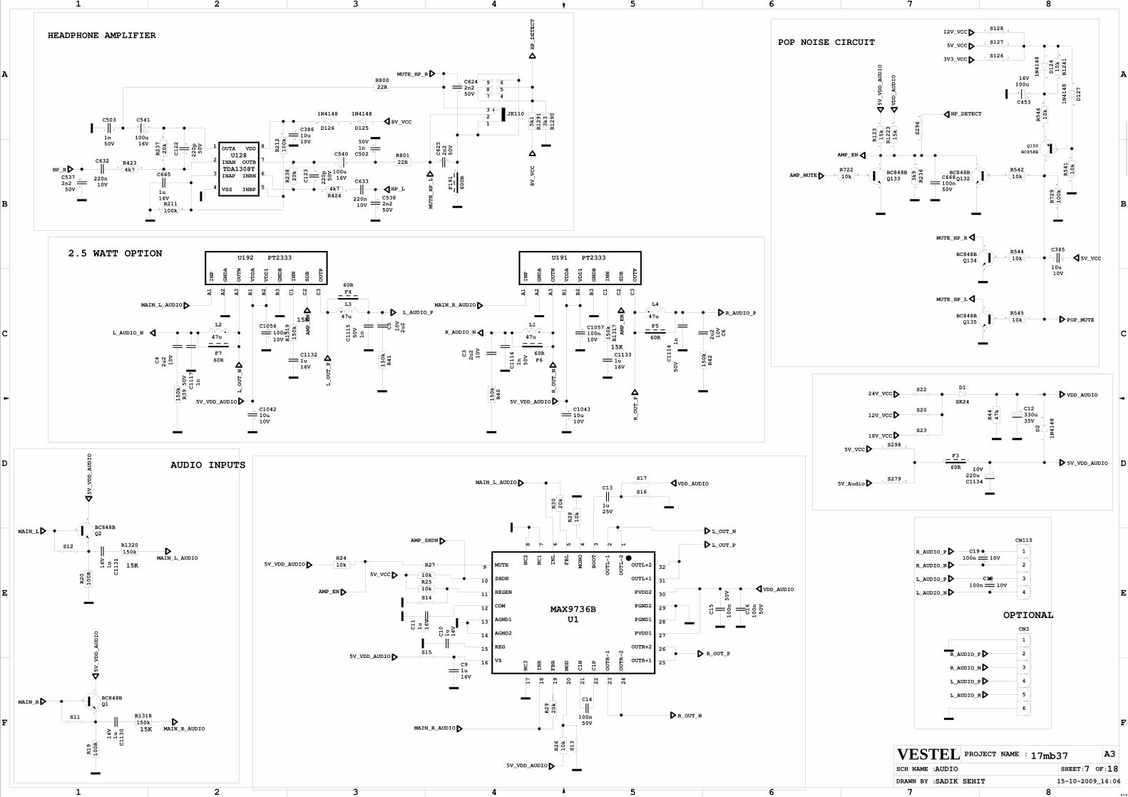
5k1
R1291
R1223
15k
21
VDD_AUDIO
R1241
10k
21
47u
L4
Q2BC848B
3
2
1
100n 10VC19
2
1
16V100u
C5412 1
R_AUDIO_P
L_AUDIO_P
L_AUDIO_N
R_AUDIO_N
PT2333U192
A1
A2
A3
B1
B2
B3
C1
C2
C3
OUTP
SDB
INN
GNDB
VDD1
VDDA
OUTN
GNDA
INP
47u
L2
60R
F5L1
47u
C1057100n 10V
2
1
R_AUDIO_N
C1116
1n
50V
R_AUDIO_P
50V
1n
C1114
5V_VDD_AUDIO
10V
2u2
C6AMP_EN
C11331u 16V
150k
R1317
150kR1318
C1130
1u
16V
10V10u C10432
1
MAIN_R
PT2333U191
A1
A2
A3
B1
B2
B3
C1
C2
C3
OUTP
SDB
INN
GNDB
VDD1
VDDA
OUTN
GNDA
INP
5V_VDD_AUDIO
5V_VCCF3
60R
21
C1115
1n
50V
50V
1n
C1117
C104210u 10V
2
1
5V_VDD_AUDIO
AMP_EN
16V1u C1132
R1319
150kC1056
10V100n
2
1
16V
1u
C1131
R1320150k
MAIN_L
L_AUDIO_N
L_AUDIO_P
5V_Audio
S298 21
S279 21
HP_DETECT
S296
21
8V_VCC
R1290
3k3
HP_DETECT
JK110
987
654
321
S12
C3
2u2
10V
5V_VDD_AUDIO
100R
R20
BC848BQ1
3
2
1
5V_VDD_AUDIO
S11
R19
100R
10V
2u2
C5
220u 10V
C1134
C4
2u2
10V
CN3
6
5
4
3
2
1
R_AUDIO_P
R_AUDIO_N
L_AUDIO_P
L_AUDIO_N
47u
L3
F660R
60RF4
F760R
16V100u
C540
21
C12330u 35V
VDD_AUDIO24V_VCCD1
SK24
MAIN_L_AUDIO
R28
10k
C13
1u 25V
50V100n
C14
50V
100n
C15
50V
100n
C16
R30
20k
R29
20k
MAIN_R_AUDIO
16V
1u
C10
16V1u C9
16V
1u
C11
S155V_VDD_AUDIO
S22
5V_VCC
5V_VDD_AUDIO
MAIN_L_AUDIO
MAIN_R_AUDIO
10kR24
5V_VDD_AUDIO
AMP_EN
10k
R26
10k
R27
10kR25
MAX9736BU1
8 7 6 5 4 3 2 1
16
15
14
13
12
11
10
9
17
18
19
20
21
22
23
24
25
26
27
28
29
30
31
32OUTL+2
OUTL+1
PVDD2
PGND2
PGND1
PVDD1
OUTR+2
OUTR+1
OUTR-2
OUTR-1
C1P
C1N
MOD
FBR
INR
NC3
MUTE
SHDN
REGEN
COM
AGND1
AGND2
REG
VS
OUTL-2
OUTL-1
BOOT
MONO
FBL
INL
NC1
NC2
S13
L_OUT_N
S14
L_OUT_P
L_OUT_P
L_OUT_N
R_OUT_P
R_OUT_N
VDD_AUDIO
MAIN_L_AUDIO
MAIN_R_AUDIO
AMP_SHDN
C1810V100n
2
1
R_OUT_N
R_OUT_P
VDD_AUDIO
12V_VCCS20
18V_VCCS23
1N4148
D2
21
S16
S17
R42
150k
150k
R41
R40
150k
R39
150k
47k
R44
10V10u
C385
21
S126 21
S127 21
17mb37
SADIK SEHIT
AUDIO 18715-10-2009_16:06
87654321
A
B
C
D
E
F
AX M
1 2 3 4 5 6 7 8
A
B
C
D
E
F
OF:
A3PROJECT NAME :VESTELSCH NAME :
DRAWN BY :
SHEET:
8V_VCC
3V3_VCC
Q133BC848B
3
2
1
AMP_MUTE
MUTE_HP_L
R54510k
2 1BC848BQ135
3
2
1
10k
R546
21
BC858BQ150
3
2
1
AMP_EN
10kR542
2 1BC848BQ132
3
2
1
1N4148
D124
21
5V_VCC
16V1u
C665
MUTE_HP_R
Q134BC848B
3
2
1
10kR544
2 1
5V_VCC
POP_MUTE
MUTE_HP_L
CN115
4
3
2
1
HP_L
HP_R
R541
10k
21
100k
R729
21
S128 21
5V_VDD_AUDIO
D127
1N4148
21
50V100n C668
12V_VCC
16V100u
C453
2 1
22RR800
50V1n
C503
21
50V
220p
C122 2
1
50V2n2 C537 2
1 600R
F191
21
15k
R123
21
100kR211
21
3k9
R236
21
20k
R237
21
4k7R423
21
4k7R424
21
10kR722
21
TDA1308T
U128
8
7
6
54
3
2
1 OUTA
INAN
INAP
VSS INBP
INBN
OUTB
VDD10V10u C3862
1
1N4148
D1262 1
D125
1N4148
2 1
C5021n 50V
2
1
C123
220p
50V2
120k
R238
21
10V220n
C633
100k
R212
21
50V2n2 C5382
1
50V
2n2
C625
2 1
MUTE_HP_R
50V2n2 C6242
1
R80122R
10V220n
C632
15K
15K
15K
15K
2.5 WATT OPTION
OPTIONAL
AUDIO INPUTS
HEADPHONE AMPLIFIERPOP NOISE CIRCUIT
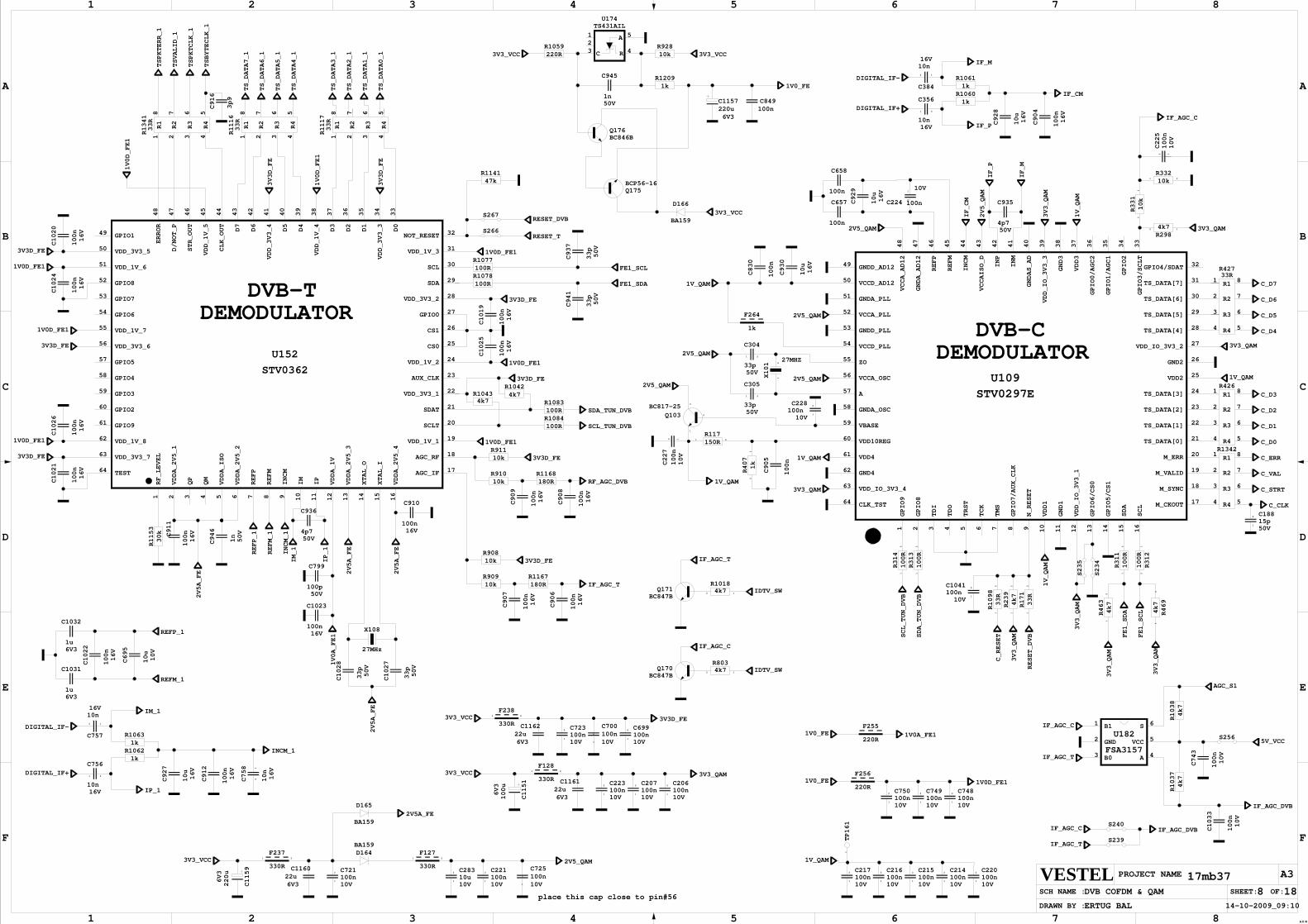
10V100n C1041 2
1
100n
10V
C1033
100n
C905
6V322u C1160
6V3220u C1157
6V3
100u
C1151
3p9
C916
C_ERR
100n
C658
100n
C657
U152
STV0362
16
15
14
13
12
11
10987654321
32
31
30
29
28
27
26
25
24
23
22
21
20
19
18
17
33
34
35
36
37
38
39
40
41
42
43
44
45
46
47
48
49
50
51
52
53
54
55
56
57
58
59
60
61
62
63
64 TEST
VDD_3V3_7
VDD_1V_8
GPIO9
GPIO2
GPIO3
GPIO4
GPIO5
VDD_3V3_6
VDD_1V_7
GPIO6
GPIO7
GPIO8
VDD_1V_6
VDD_3V3_5
GPIO1
ERROR
D/NOT_P
STR_OUT
VDD_1V_5
CLK_OUT
D7
D6
VDD_3V3_4
D5
D4
VDD_1V_4
D3
D2
D1
VDD_3V3_3
D0
AGC_IF
AGC_RF
VDD_1V_1
SCLT
SDAT
VDD_3V3_1
AUX_CLK
VDD_1V_2
CS0
CS1
GPIO0
VDD_3V3_2
SDA
SCL
VDD_1V_3
NOT_RESET
RF_LEVEL
VDDA_2V5_1
QP
QM
VDDA_ISO
VDDA_2V5_2
REFP
REFM
INCM
IM
IP
VDDA_1V
VDDA_2V5_3
XTAL_O
XTAL_I
VDDA_2V5_4
1V0_FE
6V322u C1161
3V3_QAM
3V3_QAM
10V10u C2832
1
C116222u 6V3
10V100n C2142
1
10V100n C2152
1
10V100n C2162
1
C725100n 10V
2
1
2V5_QAM
10V100n C2202
1
3V3_VCC
RESET_DVB
1V_QAM 100R
R312
21
SCL_TUN_DVB
SDA_TUN_DVB
C_D3
C_D0
C_D1
3V3_QAM
1V_QAM
3V3_QAM
C_CLK
C_STRT
C_VAL
BC817-25
Q103
3
2
1
10V100n C228 2
1
2V5_QAM
3V3_QAM
1V_QAM
2V5_QAM
2V5_QAM
1V_QAM
17mb37
ERTUG BAL
DVB COFDM & QAM 18814-10-2009_09:10
87654321
A
B
C
D
E
F
AX M
1 2 3 4 5 6 7 8
A
B
C
D
E
F
OF:
A3PROJECT NAME :VESTELSCH NAME :
DRAWN BY :
SHEET:
3V3D_FE
IF_AGC_C
3V3_QAM
FE1_SDA
FE1_SCL
2V5_QAM
50V4p7
C936
50V4p7
C935
R13428
7
6
54
3
2
1
R2
R3
R1
R4
50V15p C1882
1
27MHZ
X101 2
1
50V33p
C304
21
50V33p
C305
21
10V
100n
C227
2 1
150RR117
21
1k
R407
21
100R
R314
21
100R
R313
21
4k7
R239
21
33R
R171
21
100R
R311
21
R463
4k7
21
R469
4k7
21
R1341
33R8 7 6 5
4321
R2
R3
R1
R4
10k
R331
21
10kR332
21
10V
100n
C225
2 1
4k7R298
2 1
16V10n
C356
21
16V10n
C384
2 1
16V
10u
C928
16V
100n
C904
10V
100n C2242
1
C_D4
C_D5
C_D6
C_D7
C_D2
R4268
7
6
54
3
2
1
R2
R3
R1
R4
3V3_QAM
C830
100n
2V5_QAM
2V5_QAM
1V_QAM
1V_QAM
3V3_QAM
STV0297EU109
16
15
14
13
12
11
10987654321
32
31
30
29
28
27
26
25
24
23
22
21
20
19
18
17
33
34
35
36
37
38
39
40
41
42
43
44
45
46
47
48
49
50
51
52
53
54
55
56
57
58
59
60
61
62
63
64 CLK_TST
VDD_IO_3V3_4
GND4
VDD4
VDD10REG
VBASE
GNDA_OSC
A
VCCA_OSC
ZO
VCCD_PLL
GNDD_PLL
VCCA_PLL
GNDA_PLL
VCCD_AD12
GNDD_AD12
VCCA_AD12
GNDA_AD12
REFP
REFM
INCM
VCCAISO_D
INP
INM
GNDAS_AD
VDD_IO_3V3_3
GND3
VDD3
GPIO0/AGC2
GPIO1/AGC1
GPIO2
GPIO3/SCLT
M_CKOUT
M_SYNC
M_VALID
M_ERR
TS_DATA[0]
TS_DATA[1]
TS_DATA[2]
TS_DATA[3]
VDD2
GND2
VDD_IO_3V3_2
TS_DATA[4]
TS_DATA[5]
TS_DATA[6]
TS_DATA[7]
GPIO4/SDAT
GPIO9
GPIO8
TDI
TDO
TRST
TCK
TMS
GPIO7/AUX_CLK
N_RESET
VDD1
GND1
VDD_IO_3V3_1
GPIO6/CS0
GPIO5/CS1
SDA
SCL
330R
F12821
10V100n C2232
1
10V100n C2072
1
10V100n C2062
1
330R
F12721
10V100n C2212
1
10V100n C2172
1
220R
F255
1V0A_FE1
1V0_FE
IF_AGC_DVBIF_AGC_C
IF_AGC_T
S240
S239
1V0D_FE1
10V100n C7502
1
DIGITAL_IF+
DIGITAL_IF-
33RR427
8
7
6
54
3
2
1
R2
R3
R1
R4
TP161
1
F256
220R
30k
R1153
16V
100n
C911
50V
1n
C946
2V5A_FE
REFP_1
REFM_1
INCM_1
IM_1
2V5A_FE
2V5A_FE
27MHz
X108
50V
33p
C1028
C1027
33p
50V
2V5A_FE
IP_1
1V0A_FE1
16V
100n
C1022
3V3D_FE
C1021
100n
16V
1V0D_FE1
16V
100n
C1026
3V3D_FE
1V0D_FE1
3V3D_FE
1V0D_FE1
16V
100n
C1020
C1024
100n
16V
50V100p
C799
1V0D_FE1
33R
R1116
8 7 6 54321
R2
R3
R1
R4
33R
R1117
8 7 6 54321
R2
R3
R1
R4
3V3D_FE
3V3D_FE
TS_DATA7_1
TS_DATA6_1
TS_DATA5_1
TS_DATA4_1
TS_DATA3_1
TS_DATA2_1
TS_DATA1_1
TS_DATA0_1
C1019
100n
16V
16V
100n
C1025
3V3D_FE
1V0D_FE1
1V0D_FE1
3V3D_FE
1V0D_FE1
SCL_TUN_DVB
SDA_TUN_DVB
4k7R1042
4k7R1043
100RR1083
100RR1084
INCM_1
IM_1
IP_1
C912
100n
16V
C927
10u
16V
C756
10n 16V
21
C757
10n 16V
2 1
DIGITAL_IF+
DIGITAL_IF-R10631k
R10621k
16V
10n
C758
21
6V31u
C1032
C1031
1u 6V3
10V
10u
C695
C1023
100n 16VREFP_1
REFM_1
TSPKTERR_1
TSPKTCLK_1
TSVALID_1
TSBYTECLK_1
C910
100n 16V
IDTV_SW
C700100n 10V
2
1 10V100n C6992
1
6V3
220u
C1159
IF_AGC_C
4k7R803
2 1
TS431AILU174
3 421 5A
RC
BCP56-16Q175
3V3_VCCRESET_DVB
C849100n
BA159
D166
BA159D164
BA159
D165
3V3_VCC
2V5A_FE
10kR909
R90810k
180RR1167
3V3D_FE
16V
100n
C907
16V
100n
C906
IF_AGC_T
R1077100R
100RR1078
FE1_SDA
FE1_SCL
RESET_T
47kR1141
3V3_VCC 220RR1059
10kR928
3V3_VCC
50V1n
C945
RF_AGC_DVB
10kR911
3V3D_FE
C908
100n
16V
C909
100n
16V
R1168180R
R91010k
1kR1209
BC846BQ176
S266
S267
3V3_QAM
C723100n 10V
2
1
F238
330R
213V3_VCC
16V
10u
C929
1V_QAM
C930
10u
16V
1k
F264
Q170BC847B
IF_P
IF_M
IF_M
IF_P
1kR1061
1kR1060 IF_CM
IF_CM
C749100n 10V
2
1
10V100n C7482
1
330R
F23721
C721100n 10V
2
1
1V0D_FE1
50V
33p
C937
C941
33p
50V
R1098
33R
21
C_RESET
4k7R1018
2 1 IDTV_SW
IF_AGC_T
FSA3157
U1826
5
43
2
1 B1
GND
B0 A
VCC
SIF_AGC_C
IF_AGC_T
AGC_S1
5V_VCC
IF_AGC_DVB
4k7
R1038
4k7
R1037
10V
100n
C743
S256
S235
1V0_FE
S234
BC847BQ171
DEMODULATORDVB-T
DEMODULATORDVB-C
place this cap close to pin#56
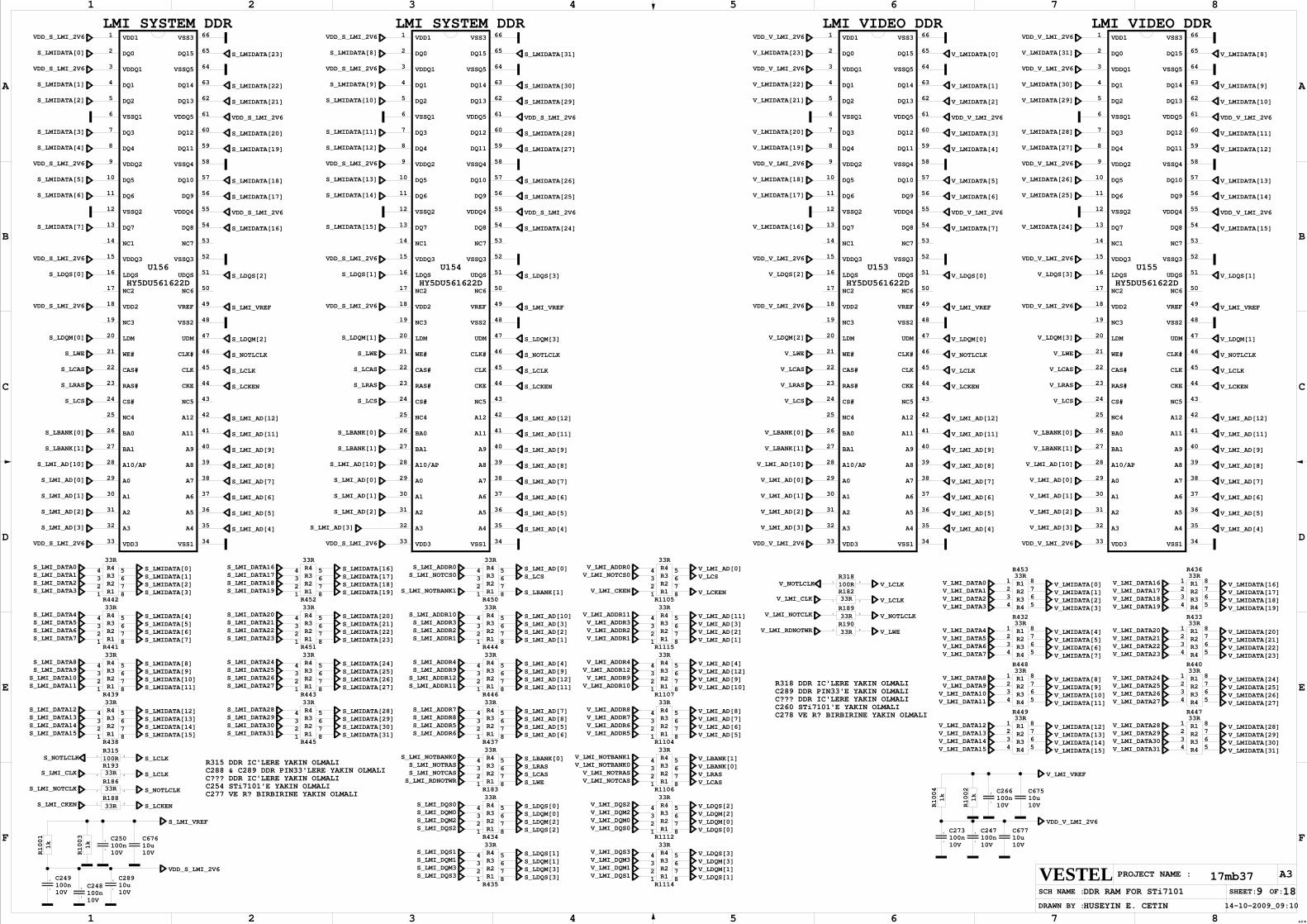
2
1
10V100n C250
C247100n 10V
2
1
V_LMIDATA[8]
V_LMIDATA[9]
V_LMIDATA[10]
V_LMIDATA[11]
V_LMIDATA[12]
HY5DU561622D
U156
1
2
3
4
5
6
7
8
9
10
11
12
13
14
15
16
17
18
19
20
21
22
23
24
25
26
27
28
29
30
31
32
33
66
65
64
63
62
61
60
59
58
57
56
55
54
53
52
51
50
49
48
47
46
45
44
43
42
41
40
39
38
37
36
35
34VSS1
A4
A5
A6
A7
A8
A9
A11
A12
NC5
CKE
CLK
CLK#
UDM
VSS2
VREF
NC6
UDQS
VSSQ3
NC7
DQ8
VDDQ4
DQ9
DQ10
VSSQ4
DQ11
DQ12
VDDQ5
DQ13
DQ14
VSSQ5
DQ15
VSS3
VDD3
A3
A2
A1
A0
A10/AP
BA1
BA0
NC4
CS#
RAS#
CAS#
WE#
LDM
NC3
VDD2
NC2
LDQS
VDDQ3
NC1
DQ7
VSSQ2
DQ6
DQ5
VDDQ2
DQ4
DQ3
VSSQ1
DQ2
DQ1
VDDQ1
DQ0
VDD1
S_LMIDATA[1]
S_LMIDATA[2]
S_LMIDATA[3]
S_LMIDATA[4]
S_LMIDATA[5]
S_LMIDATA[6]
S_LMIDATA[7]
S_LDQS[0]
S_LDQM[0]
S_LWE
S_LCAS
S_LRAS
S_LCS
S_LBANK[0]
V_LMIDATA[13]
S_LBANK[1]
S_LMI_AD[10]
S_LMI_AD[0]
S_LMI_AD[1]
S_LMI_AD[2]
S_LMI_AD[3] S_LMI_AD[4]
S_LMI_AD[5]
S_LMI_AD[6]
S_LMI_AD[7]
S_LMI_AD[8]
S_LMI_AD[9]
S_LMI_AD[11]
S_LMI_AD[12]
S_LCKEN
S_LCLK
S_NOTLCLK
S_LDQM[2]
S_LMI_VREF
S_LDQS[2]
S_LMIDATA[16]
S_LMIDATA[17]
S_LMIDATA[18]
S_LMIDATA[19]
S_LMIDATA[20]
S_LMIDATA[21]
S_LMIDATA[22]
S_LMIDATA[23]
V_LMIDATA[14]
10V100n C2482
1
10V100n C2492
1
V_LMIDATA[15]
VDD_V_LMI_2V6
S_LMIDATA[31]
S_LMIDATA[30]
S_LMIDATA[29]
S_LMIDATA[28]
S_LMIDATA[27]
100RR318
21
S_LMIDATA[26]
S_LMIDATA[25]
S_LMIDATA[24]
VDD_S_LMI_2V6
S_LDQS[3]
S_LDQM[3]
S_LMI_VREF
S_NOTLCLK
S_LCLK
S_LCKEN
S_LMI_AD[12]
S_LMI_AD[11]
S_LMI_AD[9]
S_LMI_AD[8]
S_LMI_AD[7]
S_LMI_AD[6]
S_LMI_AD[5]
S_LMI_AD[4]S_LMI_AD[3]
S_LMI_AD[2]
S_LMI_AD[1]
S_LMI_AD[0]
S_LMI_AD[10]
S_LBANK[1]
S_LBANK[0]
S_LCS
S_LDQM[1]
S_LRAS
S_LCAS
S_LWE
S_LDQS[1]
S_LMIDATA[15]
S_LMIDATA[14]
S_LMIDATA[13]
S_LMIDATA[12]
S_LMIDATA[11]
S_LMIDATA[10]
S_LMIDATA[9]
S_LMIDATA[8]
VDD_S_LMI_2V6
VDD_S_LMI_2V6
VDD_S_LMI_2V6
VDD_S_LMI_2V6
VDD_S_LMI_2V6
VDD_S_LMI_2V6
VDD_S_LMI_2V6
HY5DU561622D
U154
1
2
3
4
5
6
7
8
9
10
11
12
13
14
15
16
17
18
19
20
21
22
23
24
25
26
27
28
29
30
31
32
33
66
65
64
63
62
61
60
59
58
57
56
55
54
53
52
51
50
49
48
47
46
45
44
43
42
41
40
39
38
37
36
35
34VSS1
A4
A5
A6
A7
A8
A9
A11
A12
NC5
CKE
CLK
CLK#
UDM
VSS2
VREF
NC6
UDQS
VSSQ3
NC7
DQ8
VDDQ4
DQ9
DQ10
VSSQ4
DQ11
DQ12
VDDQ5
DQ13
DQ14
VSSQ5
DQ15
VSS3
VDD3
A3
A2
A1
A0
A10/AP
BA1
BA0
NC4
CS#
RAS#
CAS#
WE#
LDM
NC3
VDD2
NC2
LDQS
VDDQ3
NC1
DQ7
VSSQ2
DQ6
DQ5
VDDQ2
DQ4
DQ3
VSSQ1
DQ2
DQ1
VDDQ1
DQ0
VDD1
HY5DU561622D
U153
1
2
3
4
5
6
7
8
9
10
11
12
13
14
15
16
17
18
19
20
21
22
23
24
25
26
27
28
29
30
31
32
33
66
65
64
63
62
61
60
59
58
57
56
55
54
53
52
51
50
49
48
47
46
45
44
43
42
41
40
39
38
37
36
35
34VSS1
A4
A5
A6
A7
A8
A9
A11
A12
NC5
CKE
CLK
CLK#
UDM
VSS2
VREF
NC6
UDQS
VSSQ3
NC7
DQ8
VDDQ4
DQ9
DQ10
VSSQ4
DQ11
DQ12
VDDQ5
DQ13
DQ14
VSSQ5
DQ15
VSS3
VDD3
A3
A2
A1
A0
A10/AP
BA1
BA0
NC4
CS#
RAS#
CAS#
WE#
LDM
NC3
VDD2
NC2
LDQS
VDDQ3
NC1
DQ7
VSSQ2
DQ6
DQ5
VDDQ2
DQ4
DQ3
VSSQ1
DQ2
DQ1
VDDQ1
DQ0
VDD1VDD_V_LMI_2V6
VDD_V_LMI_2V6
VDD_V_LMI_2V6
VDD_V_LMI_2V6
VDD_V_LMI_2V6
VDD_V_LMI_2V6
VDD_V_LMI_2V6
V_LMIDATA[23]
V_LMIDATA[22]
V_LMIDATA[21]
V_LMIDATA[20]
V_LMIDATA[19]
V_LMIDATA[18]
V_LMIDATA[17]
V_LMIDATA[16]
V_LDQS[2]
V_LWE
V_LCAS
V_LRAS
V_LDQM[2]
V_LCS
V_LBANK[0]
V_LBANK[1]
V_LMI_AD[10]
V_LMI_AD[0]
V_LMI_AD[1]
V_LMI_AD[2]
V_LMI_AD[3] V_LMI_AD[4]
V_LMI_AD[5]
V_LMI_AD[6]
V_LMI_AD[7]
V_LMI_AD[8]
V_LMI_AD[9]
V_LMI_AD[11]
V_LMI_AD[12]
V_LCKEN
V_LCLK
V_NOTLCLK
V_LMI_VREF
V_LDQM[0]
V_LDQS[0]
VDD_V_LMI_2V6
V_LMIDATA[7]
V_LMIDATA[6]
V_LMIDATA[5]
V_LMIDATA[4]
V_LMIDATA[3]
V_LMIDATA[2]
33RR182
21
33RR453
87654
321
R4R3R2R1
V_LMIDATA[1]
S_NOTLCLK
V_LMIDATA[0]
S_LMIDATA[15]
V_LDQS[1]
V_LDQM[1]
V_LMI_VREF
V_NOTLCLK
V_LCLK
V_LCKEN
V_LMI_AD[12]
V_LMI_AD[11]
V_LMI_AD[9]
S_LMI_DQS3S_LMI_DQM3
33RR436
87654
321
R4R3R2R1
S_LCLK
S_LMI_DQM1S_LMI_DQS1
S_LMI_DQS2S_LMI_DQM2S_LMI_DQM0S_LMI_DQS0
V_LMI_AD[8]
V_LMI_AD[7]
V_LMI_AD[6]
V_LMI_AD[5]
V_LMI_AD[4]V_LMI_AD[3]
V_LMI_AD[2]
V_LMI_AD[1]
V_LMI_AD[0]
V_LMI_AD[10]
V_LBANK[1]
V_LBANK[0]
V_LCS
V_LDQM[3]
V_LRAS
V_LCAS
V_LWE
V_LDQS[3]
V_LMIDATA[24]
V_LMIDATA[25]
S_LMI_ADDR6S_LMI_ADDR5S_LMI_ADDR8S_LMI_ADDR7
S_LMI_ADDR11S_LMI_ADDR12S_LMI_ADDR9S_LMI_ADDR4
33RR188
21
S_LMI_ADDR1S_LMI_ADDR2S_LMI_ADDR3
S_LMI_ADDR10
S_LMIDATA[14]S_LMIDATA[13]
S_LCKEN
S_LMIDATA[12]
33RR186
21
S_LMI_ADDR0
S_LMI_AD[6]
S_LMIDATA[11]
V_LMIDATA[26]
S_LMIDATA[31]S_LMIDATA[30]S_LMIDATA[29]S_LMIDATA[28]
S_LMIDATA[10]S_LMIDATA[9]S_LMIDATA[8]
S_LMIDATA[7]
V_LMIDATA[27]
V_LMIDATA[28]
V_LMIDATA[29]
V_LMIDATA[30]
V_LMIDATA[31]
VDD_V_LMI_2V6
VDD_V_LMI_2V6
VDD_V_LMI_2V6
VDD_V_LMI_2V6
VDD_V_LMI_2V6
VDD_V_LMI_2V6
VDD_V_LMI_2V6
HY5DU561622D
U155
1
2
3
4
5
6
7
8
9
10
11
12
13
14
15
16
17
18
19
20
21
22
23
24
25
26
27
28
29
30
31
32
33
66
65
64
63
62
61
60
59
58
57
56
55
54
53
52
51
50
49
48
47
46
45
44
43
42
41
40
39
38
37
36
35
34VSS1
A4
A5
A6
A7
A8
A9
A11
A12
NC5
CKE
CLK
CLK#
UDM
VSS2
VREF
NC6
UDQS
VSSQ3
NC7
DQ8
VDDQ4
DQ9
DQ10
VSSQ4
DQ11
DQ12
VDDQ5
DQ13
DQ14
VSSQ5
DQ15
VSS3
VDD3
A3
A2
A1
A0
A10/AP
BA1
BA0
NC4
CS#
RAS#
CAS#
WE#
LDM
NC3
VDD2
NC2
LDQS
VDDQ3
NC1
DQ7
VSSQ2
DQ6
DQ5
VDDQ2
DQ4
DQ3
VSSQ1
DQ2
DQ1
VDDQ1
DQ0
VDD1
S_LMIDATA[6]S_LMIDATA[5]S_LMIDATA[4]
S_LMI_DATA15S_LMI_DATA14S_LMI_DATA13S_LMI_DATA12
S_LMI_DATA11S_LMI_DATA10S_LMI_DATA9
S_LMIDATA[27]S_LMIDATA[26]S_LMIDATA[25]
S_LMI_DATA8 S_LMIDATA[24]
S_LMI_AD[5]S_LMI_AD[8]
100RR315
21
33RR193
21
S_LMIDATA[23]33RR190
21
S_LMI_AD[7]
S_LMIDATA[22]S_LMIDATA[21]S_LMIDATA[20]
S_LMIDATA[19]S_LMIDATA[18]S_LMIDATA[17]S_LMIDATA[16]
S_LMI_DATA31S_LMI_DATA30
S_LMI_DATA7
S_LMI_DATA29S_LMI_DATA28
S_LMI_DATA6S_LMI_DATA5S_LMI_DATA4
S_LMI_DATA3S_LMI_DATA2S_LMI_DATA1S_LMI_DATA0
S_LMIDATA[3]S_LMIDATA[2]S_LMIDATA[1]S_LMIDATA[0]
33R
R43887654
321
R4R3R2R1
17mb37
HUSEYIN E. CETIN
DDR RAM FOR STi7101 18914-10-2009_09:10
87654321
A
B
C
D
E
F
AX M
1 2 3 4 5 6 7 8
A
B
C
D
E
F
OF:
A3PROJECT NAME :VESTELSCH NAME :
DRAWN BY :
SHEET:
S_LMI_DATA27S_LMI_DATA26S_LMI_DATA25S_LMI_DATA24
S_LMI_DATA23
R43333R
87654
321
R4R3R2R1S_LMI_DATA22
S_LMI_RDNOTWR
S_LMI_DATA21S_LMI_DATA20
S_LMI_DATA19S_LMI_DATA18S_LMI_DATA17S_LMI_DATA16
33R
R43987654
321
R4R3R2R1
33R
R44587654
321
R4R3R2R1
33R
R44387654
321
R4R3R2R1
33R
R45187654
321
R4R3R2R1
33R
R45287654
321
R4R3R2R1
33R
R44187654
321
R4R3R2R1
33R
R44287654
321
R4R3R2R1
S_LMI_AD[11]S_LMI_AD[12]S_LMI_AD[9]S_LMI_AD[4]
S_LMI_AD[1]S_LMI_AD[2]S_LMI_AD[3]S_LMI_AD[10]
S_LMI_NOTBANK1
S_LMI_NOTCS0
S_LBANK[1]
R43233R
87654
321
R4R3R2R1
33RR448
87654
321
R4R3R2R1
33RR189
21
S_LMI_AD[0]S_LCS
33RR449
87654
321
R4R3R2R1
33R
R45087654
321
R4R3R2R1
33R
R44487654
321
R4R3R2R1
S_LMI_NOTCASS_LMI_NOTRAS
S_LMI_NOTBANK0
S_LDQS[3]S_LDQM[3]S_LDQM[1]S_LDQS[1]
S_LDQS[2]S_LDQM[2]S_LDQM[0]S_LDQS[0]
S_LBANK[0]
33RR440
87654
321
R4R3R2R1
33R
R44687654
321
R4R3R2R1
33R
R43787654
321
R4R3R2R1
S_LWES_LCAS
33R
R18387654
321
R4R3R2R1
S_LRAS
33R
R43487654
321
R4R3R2R1
R435
33R
87654
321
R4R3R2R1
S_LCLK
S_NOTLCLK
S_LMI_CLK
S_LMI_NOTCLK
S_LMI_CKEN
10V10u C2892
1
10V100n C2732
1
VDD_S_LMI_2V6
S_LMI_VREF
1k
R1001
1k
R1003
10V10u C676
V_LMIDATA[0]V_LMIDATA[1]V_LMIDATA[2]V_LMIDATA[3]
V_LMI_DATA0V_LMI_DATA1V_LMI_DATA2V_LMI_DATA3
V_LMI_DATA4V_LMI_DATA5V_LMI_DATA6V_LMI_DATA7
V_LMI_DATA8V_LMI_DATA9
V_LMI_DATA10V_LMI_DATA11
V_LMI_DATA12V_LMI_DATA13V_LMI_DATA14V_LMI_DATA15
V_LMIDATA[4]V_LMIDATA[5]V_LMIDATA[6]V_LMIDATA[7]
V_LMIDATA[8]V_LMIDATA[9]V_LMIDATA[10]
10V100n C2662
1
V_LMIDATA[11]
V_LMIDATA[12]V_LMIDATA[13]V_LMIDATA[14]V_LMIDATA[15]
33RR447
87654
321
R4R3R2R1
V_LMI_DATA16V_LMI_DATA17V_LMI_DATA18V_LMI_DATA19
V_LMI_DATA20V_LMI_DATA21V_LMI_DATA22V_LMI_DATA23
V_LMI_DATA24V_LMI_DATA25V_LMI_DATA26V_LMI_DATA27
V_LMI_DATA28V_LMI_DATA29V_LMI_DATA30V_LMI_DATA31
V_LMIDATA[16]V_LMIDATA[17]V_LMIDATA[18]V_LMIDATA[19]
V_LMIDATA[20]V_LMIDATA[21]V_LMIDATA[22]V_LMIDATA[23]
V_LMIDATA[24]
VDD_S_LMI_2V6
VDD_S_LMI_2V6
VDD_S_LMI_2V6
VDD_S_LMI_2V6
VDD_S_LMI_2V6
VDD_S_LMI_2V6
VDD_S_LMI_2V6
VDD_S_LMI_2V6
S_LMIDATA[0]
V_LMIDATA[25]V_LMIDATA[26]V_LMIDATA[27]
V_LMIDATA[28]V_LMIDATA[29]V_LMIDATA[30]V_LMIDATA[31]
1k
R1002
10V10u C675
1k
R1004
10V10u C677
V_LWE
V_LMI_VREF
V_LMI_NOTCLK
V_LMI_CLK
VDD_V_LMI_2V6
V_NOTLCLK
V_LCLK
V_LMI_RDNOTWR
33R
R111487654
321
R4R3R2R1
R1112
33R
87654
321
R4R3R2R1
V_LBANK[0]
R1106
33R
87654
321
R4R3R2R1
V_LCLKV_NOTLCLK
V_LRASV_LCAS
R1104
33R
87654
321
R4R3R2R1
R1107
33R
87654
321
R4R3R2R1
V_LBANK[1]
V_LDQS[2]V_LDQM[2]V_LDQM[0]V_LDQS[0]
V_LDQS[3]V_LDQM[3]V_LDQM[1]V_LDQS[1]
V_LMI_NOTBANK1V_LMI_NOTBANK0V_LMI_NOTRAS
R1115
33R
87654
321
R4R3R2R1
R1105
33R
87654
321
R4R3R2R1
V_LCSV_LMI_AD[0]
V_LCKEN
V_LMI_NOTCS0
V_LMI_CKEN
V_LMI_AD[11]V_LMI_AD[3]V_LMI_AD[2]V_LMI_AD[1]
V_LMI_AD[4]V_LMI_AD[12]V_LMI_AD[9]V_LMI_AD[10]
V_LMI_NOTCAS
V_LMI_AD[8]V_LMI_AD[7]V_LMI_AD[6]V_LMI_AD[5]
V_LMI_ADDR0
V_LMI_ADDR11V_LMI_ADDR3V_LMI_ADDR2V_LMI_ADDR1
V_LMI_ADDR4V_LMI_ADDR12V_LMI_ADDR9
V_LMI_ADDR10
V_LMI_ADDR8V_LMI_ADDR7V_LMI_ADDR6V_LMI_ADDR5
V_LMI_DQS2V_LMI_DQM2V_LMI_DQM0V_LMI_DQS0
V_LMI_DQS3V_LMI_DQM3V_LMI_DQM1V_LMI_DQS1
C288 & C289 DDR PIN33'LERE YAKIN OLMALIC??? DDR IC'LERE YAKIN OLMALIC254 STi7101'E YAKIN OLMALIC277 VE R? BIRBIRINE YAKIN OLMALI
R315 DDR IC'LERE YAKIN OLMALI
C278 VE R? BIRBIRINE YAKIN OLMALIC260 STi7101'E YAKIN OLMALIC??? DDR IC'LERE YAKIN OLMALIC289 DDR PIN33'E YAKIN OLMALIR318 DDR IC'LERE YAKIN OLMALI
LMI SYSTEM DDR LMI SYSTEM DDR LMI VIDEO DDR LMI VIDEO DDR
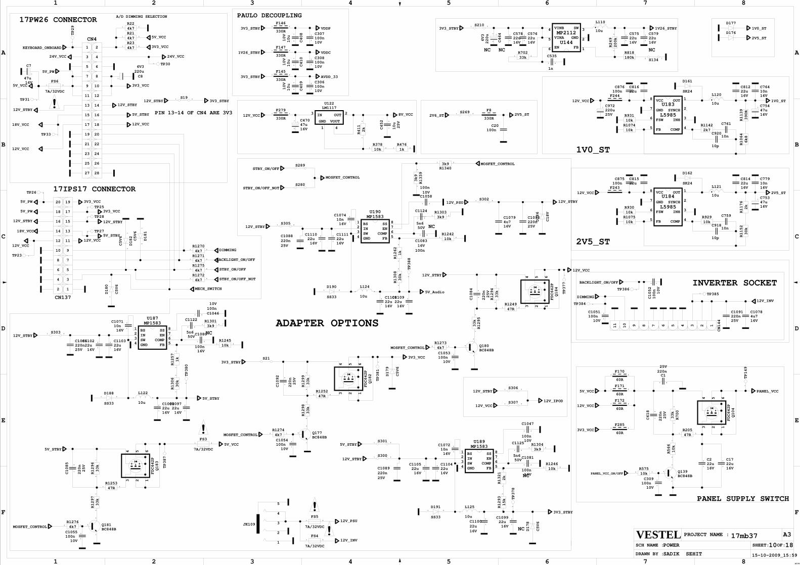
C410
10u
10V
21
C409
10u
10V
21
D180
C5V6
21
D181
C5V6
21
R12724k7
21
4k7R1275
21
R566
10k
21
3V3_STBY
C306100n 10V
2
1
STBY_ON/OFF
5V_PW
5V_PW
3V3_VCC
3V3_VCC
5V_STBY12V_VCC
4k7R1270
21
4k7R1271
21 BACKLIGHT_ON/OFF
2V5_ST2V6_STS269 21
17mb37
SADIK SEHIT
POWER 1810
15-10-2009_15:59
87654321
A
B
C
D
E
F
AX M
1 2 3 4 5 6 7 8
A
B
C
D
E
F
OF:
A3PROJECT NAME :VESTELSCH NAME :
DRAWN BY :
SHEET:
12V_VCC
MECH_SWITCH
STBY_ON/OFF_NOT
S1342 1
12V_VCC
12V_STBY
C5V6
D182
21
330R
F14521
PANEL_VCC_ON/OFFBC848BQ139
3
2
1
12V_VCC
5V_VCC
47RR205
21
C309100n 10V
2
1
330R
F27921
10kR575
2 1
1V26_STBY
3V3_STBY
DIMMING
12V_STBY
CN137
20 19
18 17
16 15
14 13
12 11
10 9
8 7
6 5
4 3
2 1
D179
C5V6
R1299
33k
21
C1092
220n
25V2
1
MOSFET_CONTROL
S280
S289
F170
60R
21
JK109
5
4
3
2
1
FS5
7A/32VDC
21
PANEL_VCC
10V100n C3082
1
330R
F14721
F146
330R
21
C408
10u
10V
21
10V100n C3072
1
12V_PSU
LM1117U122
4
3 2
1
GND
OUTIN
VOUT
8V_VCC
7A/32VDC
FS421
VDDP
VDDC
AVDD_33
MP2112
U1446
5
4 3
2
1FB
GND
SWVINB
VINA
EN
12V_INV
STBY_ON/OFF_NOT
25V220n C1093
16V22u C5792
1
16V22u C5752
1
16V22u C5762
1
60R
F17121
S302 21
12V_PSU 12V_STBY
16V22u C5782
1
C10794u7 16V
16V47u C470
2
1
1V0_ST
D177
2V5_ST
D186
C18V
STBY_ON/OFF
1n
C535
21
D176
R125247R
21
200k
R249
21
R70233k
21
Q177BC848B
3
2
1
3V3_STBY
10kR378
21
33k
R1298
21
Q182
FDC642P
2
6543 1
MOSFET_CONTROL
3V3_VCC
1kR476
21
TP381
1
4k7R1274
2 1
TP149
1
FDC642P
Q104
2
6543 1
C1054100n
10V
2
1
60R
F17221
C1220n 25V
21
R13013k9
21
25V
220n
C618 2
1
25V
10u
C452 2
1
2k
R411
21
R124510k
21
C1103
16V22u
2
1
3V3_STBY
C109822u 16V
2
122u 16V
C1097 2
1
S210 21
1V26_STBY
C1122
5n6 50V
21
C464
220u
6V3
21
10n 16V
C1071 2
1
100n 16V
C1080
21
100n 10V
C104621
D188
SS33
21
TP380
1
16V22u
C1102 2
1
U187MP1583
1234
8765FB
COMPENSS
GNDSWINBS
5V_STBY
S303 21
12V_STBY
R700
33k
21
30k
R1306
21
R1257
1k
21
C1086220n 25V 4k7
R12732 1
10u
L120
F285
60R
21
3V3_VCC
10u
L110
MOSFET_CONTROL
12V_VCC
R124947R
21
R1295
33k
21
33k
R1294
21
C1084
220n
25V2
1
Q180BC848B
3
2
1
12V_STBY
C1053100n
10V
2
1
TP377
1
Q184
FDC642P
2
6543 1
16V22u C11112
1
C110822u 16V
2
1
C110922u 16V
2
1
R13033k9
21
C1124
5n6 50V
21
C107410n 16V
2
1
C1083
100n 16V
21
C1058
100n 10V
21
D190
SS33
21
TP388
1
16V22u C1110 2
1
U190MP1583
1234
8765FB
COMPENSS
GNDSWINBS
5V_Audio
S305 21
12V_STBY
R124210k
21
R1308
30k
21
R1262
1k
21
10u
L12421
C1088220n 25V
3k9R1340
21
R1339
3k9
21
Q181BC848B
3
2
1C1055100n
10V
2
1
4k7R1276
2 1
TP387
5V_VCC5V_STBY
Q183
FDC642P
2
6543 1
33k
R1297
21
25V
220n
C1085 2
1
R1296
33k
21
47RR1253
21
7A/32VDC
FS321
MOSFET_CONTROL
12V_IPODS307 21
12V_VCC
S306 21
12V_STBY
S301 21
5V_STBY
C5V6
D178
R1321
2k
21
C1089220n 25V
10V100n
C1047
21
R1293
15k
21
12V_STBYS300 21
C110422u 16V
2
1
180kR818
16V22u C1100
2
1
16V22u C1099 2
1
3k9R1304
21
C1125
50V5n6
21
16V10n C1072 2
1
F244
16V100n
C1081
21
D191
SS33
21
TP378
1
C1105
16V22u
2
1
U189MP1583
1234
8765FB
COMPENSS
GNDSWINBS
3V3_STBY
R124610k
21
TP23 1
TP271
TP281
TP251
TP26 1
TP3851
4u7 16V
C1078
TP384 1
TP386 1
CN144
11
10 9 8 7 6 5 4 3 2 1
BACKLIGHT_ON/OFF
C1091220n 25V
DIMMING C1052
100n
10V
2 1
12V_INV
10kR931
C1051
10V100n
2
1
16V22u C22
1
16V22u C172
1
220u 6V3
C8
SK24
D161
1V0_ST
R107410k 2k7
R1142
10n
C761
10p
C920
390R
R1139
16V47u C754
L122
10u
21
10u
L12521
C7
47u 16V
5V_VCC
4k7R22
21
R214k7
21
4k7R23
21
24V_VCC
7A/32VDC
FS621
16V22u C812
3V3_VCC
24V_VCC
5V_VCC
TP29
1
16V10n C764
12V_STBY
12V_VCC
5V_STBY
3V3_VCC
KEYBOARD_ONBOARD
12V_STBY
CN4
2827
2625
2423
2221
2019
1817
1615
1413
1211
109
87
65
43
21
5V_PW
TP301
TP31 1 3V3_STBY12V_STBYS19 21
330R
F8
S21
12V_VCC
18V_VCC
18V_VCC
C20100n
TP33 1
L5985
U1838
7
6
5 4
3
2
1OUT
SYNCH
INH
COMPFB
FSW
GND
VCC12V_VCC
22u C816
25V220u C972
100n C876
MOSFET_CONTROL
U184
L5985
8
7
6
5 4
3
2
1OUT
SYNCH
INH
COMPFB
FSW
GND
VCCF243
C875100n
12V_VCC
C81522u
C81422u 16V
2V5_STC75347u 16V
10kR1075
D162
SK24
C918
10p
10kR929 C759
10n
R93010k
C77910n 16V
6k8
R1064
30k
R1152
2k
R1176
10u
L12117IPS17 CONNECTOR
NC
NC
ADAPTER OPTIONS
PAULO DECOUPLING
PANEL SUPPLY SWITCH
INVERTER SOCKET
NC
NC
NC NC
NC
!
!
!
17PW26 CONNECTORA/D DIMMING SELECTION
!PIN 13-14 OF CN4 ARE 3V3
1V0_ST
2V5_ST
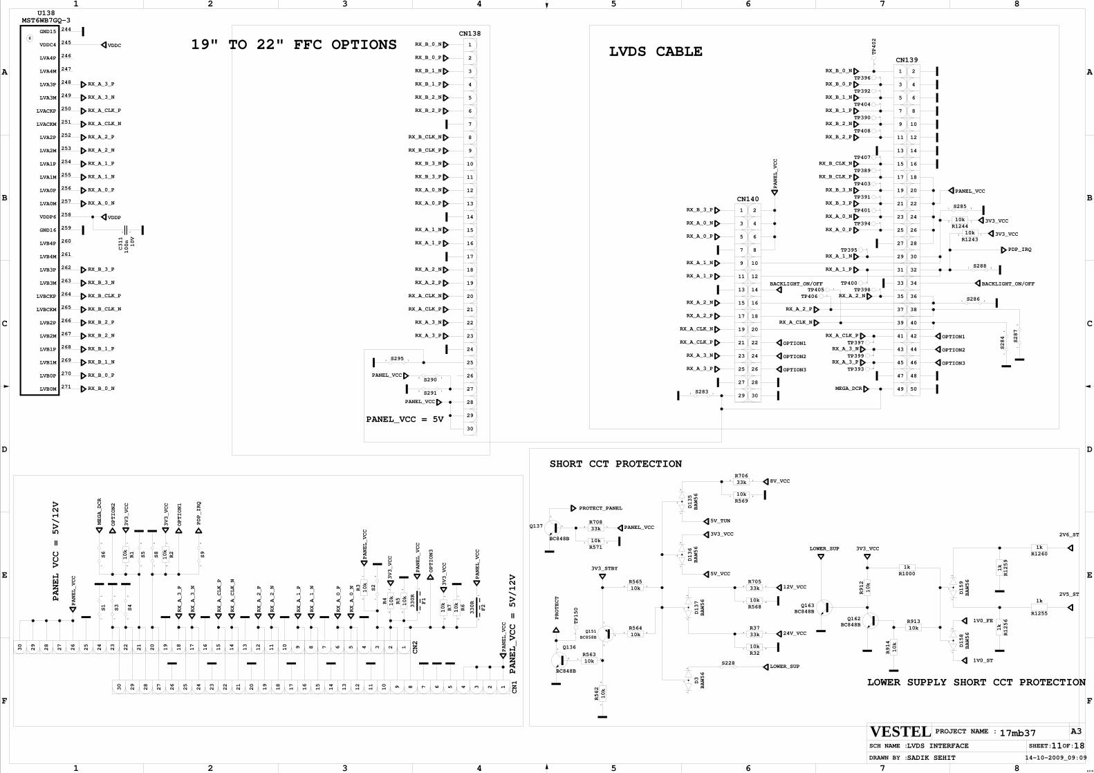
LOWER_SUP
BC848BQ163
BC848BQ162
3V3_VCC
10k
R912
10kR913
BAW56
D159
3
21
D158
BAW56
3
21
1kR1000
R914
10k
2V6_ST
2V5_ST
1V0_FE
1V0_ST
10kR571
21
33kR708
2 1
10kR569
21
D137
BAW56
3
21
R562
10k
21
R56310k
21
Q136
BC848B
3
2
1
BC858BQ151
3
2
1
1kR1260
R56410k
21
3V3_STBY
R1259
1k
5V_VCC
1k
R1255
R1256
1k
3V3_VCC
BAW56
D135
3
21
PDP_IRQ
3V3_VCCR124410k2 1
10kR1243
2 1 3V3_VCC
MEGA_DCR
S288 21
S287
21S284
21
TP406 1
RX_A_3_P
RX_A_3_N
RX_A_CLK_P
RX_A_CLK_N
RX_A_2_P
TP398 1
TP400 1
RX_A_2_N
BACKLIGHT_ON/OFF
RX_A_1_P
RX_A_1_N
TP394 1
PANEL_VCC
TP396 1
TP402
1
S285 21
S2902 1
RX_B_0_N
S2952 1
RX_A_3_N
RX_A_CLK_P
RX_A_2_P
RX_A_2_N
RX_A_1_P
RX_A_1_N
RX_A_0_P
CN138
30
29
28
27
26
25
24
23
22
21
20
19
18
17
16
15
14
13
12
11
10
9
8
7
6
5
4
3
2
1
RX_A_0_N
RX_A_CLK_N
RX_A_3_P
RX_B_3_P
RX_B_3_N
RX_B_CLK_P
RX_B_CLK_N
RX_B_2_P
RX_B_1_P
RX_B_1_N
RX_B_0_P
PANEL_VCC
PANEL_VCC
S2912 1
RX_B_2_N
PANEL_VCC
CN139
5049
4847
4645
4443
4241
4039
3837
3635
3433
3231
3029
2827
2625
2423
2221
2019
1817
1615
1413
1211
109
87
65
43
21
S2832 1
BACKLIGHT_ON/OFF
CN140
3029
2827
2625
2423
2221
2019
1817
1615
1413
1211
109
87
65
43
21
OPTION3
OPTION2
OPTION1
RX_B_0_N
RX_A_0_P
RX_A_0_N
RX_B_3_P
RX_B_3_N
RX_B_CLK_P
RX_B_CLK_N
RX_B_2_P
RX_B_2_N
RX_B_1_P
RX_B_1_N
RX_B_0_P
RX_B_3_P
RX_A_3_P
RX_A_CLK_N
RX_A_0_N
RX_A_0_P
RX_A_1_N
RX_A_1_P
RX_A_2_N
RX_A_2_P
RX_A_CLK_P
RX_A_3_N
OPTION1
OPTION2
OPTION3
S286 21
TP392 1
TP404 1
TP390 1
TP408 1
TP407 1
TP389 1
TP403 1
TP391 1
TP401 1
TP395 1
TP393 1
TP399 1
TP397 1
TP405 1
10kR565
2 1
R70533k
2 1 12V_VCC
R56810k 21
R70633k
2 1
5V_TUN
D136
BAW56
3
21
17mb37
SADIK SEHIT
LVDS INTERFACE 181114-10-2009_09:09
87654321
A
B
C
D
E
F
AX M
1 2 3 4 5 6 7 8
A
B
C
D
E
F
OF:
A3PROJECT NAME :VESTELSCH NAME :
DRAWN BY :
SHEET:
RX_A_3_P
RX_A_3_N
RX_A_CLK_P
RX_A_CLK_N
RX_A_2_P
RX_A_2_N
RX_A_1_P
RX_A_1_N
RX_A_0_P
RX_A_0_N
RX_B_3_P
RX_B_3_N
RX_B_CLK_P
RX_B_CLK_N
RX_B_2_P
RX_B_2_N
RX_B_1_P
RX_B_1_N
RX_B_0_P
RX_B_0_N
PANEL_VCC
PROTECT_PANEL
BC848B
Q137
3
2
1
8V_VCC
PROTECT
TP150
1
S9
21
LOWER_SUPS228
VDDP
VDDC
10V
100n
C311
2 1
PDP_IRQ
S6
21
MEGA_DCR
MST6WB7GQ-3U138
271
270
244
245
246
247
248
249
250
251
252
253
254
255
256
257
258
259
260
261
262
263
264
265
266
267
268
269LVB1M
LVB1P
LVB2M
LVB2P
LVBCKM
LVBCKP
LVB3M
LVB3P
LVB4M
LVB4P
GND16
VDDP6
LVA0M
LVA0P
LVA1M
LVA1P
LVA2M
LVA2P
LVACKM
LVACKP
LVA3M
LVA3P
LVA4M
LVA4P
VDDC4
GND15
LVB0P
LVB0M
6
PANEL_VCC
R3
10k
21
RX_A_2_N
RX_A_3_P
F2
330R
21
OPTION3
OPTION1
OPTION2
10k
R1
21
R7
10k
21
R5
10k
21S2
21
PANEL_VCC
PANEL_VCC
10k
R4
21
3V3_VCCS8
21
3V3_VCC
R2
10k
21
RX_A_CLK_N
RX_A_3_N
RX_A_CLK_P
RX_A_2_P
RX_A_1_P
RX_A_1_N
RX_A_0_P
3V3_VCC
S3
21
S1
21
RX_A_0_N
PANEL_VCC
S5
21
10k
R6
21
S4
21
CN2
30
29
28
27
26
25
24
23
22
21
20
19
18
17
16
15
14
13
12
11
10 9 8 7 6 5 4 3 2 1
CN1
30
29
28
27
26
25
24
23
22
21
20
19
18
17
16
15
14
13
12
11
10 9 8 7 6 5 4 3 2 1
PANEL_VCC
3V3_VCC
330R
F1
21
24V_VCC
R3210k 21
R3733k
2 1
D3
BAW56
3
21
PANEL VCC = 5V/12V
LVDS CABLE
SHORT CCT PROTECTION
19" TO 22" FFC OPTIONS
PANEL_VCC = 5V
PANEL_VCC = 5V/12V
LOWER SUPPLY SHORT CCT PROTECTION
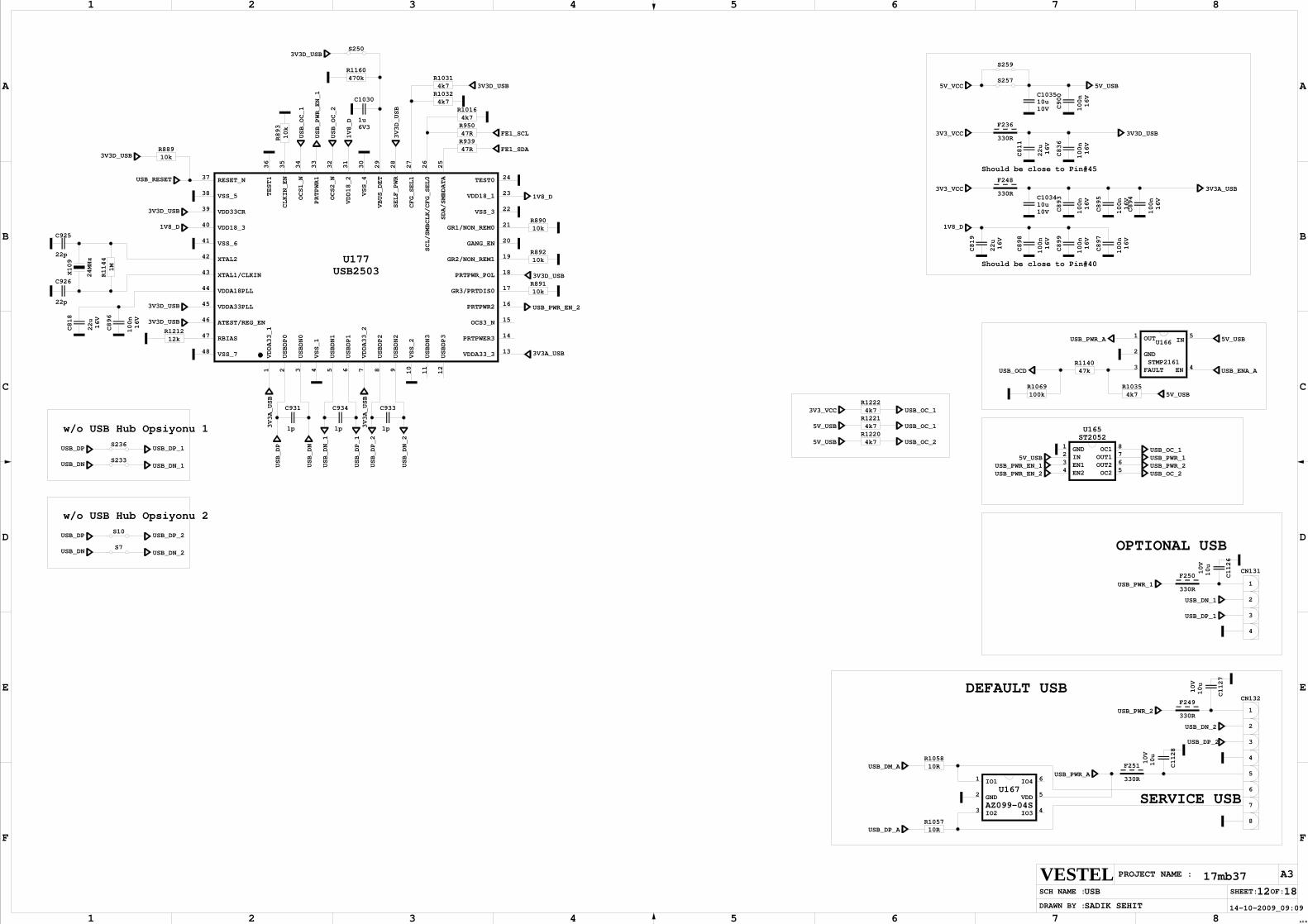
10u 10V
C1035
CN132
8
7
6
5
4
3
2
1
USB_OC_1R12214k7
4k7R1220
5V_USB
USB_OC_25V_USB
3V3_VCC 4k7R1222
USB_OC_1
10V
10u
C1126
C1127
10u
10V
10V
10u
C1128
17mb37
SADIK SEHIT
USB 1812
14-10-2009_09:09
87654321
A
B
C
D
E
F
AX M
1 2 3 4 5 6 7 8
A
B
C
D
E
F
OF:
A3PROJECT NAME :VESTELSCH NAME :
DRAWN BY :
SHEET:
S10
S7
USB_DP
USB_DN USB_DN_2
USB_DP_2
CN131
4
3
2
1
USB_DP_1
USB_DN_1USB_DN
USB_DP
1p
C931
1p
C933C934
1p
S233
S236
1V8_D
C897
100n
16V
16V
22u
C819
R10324k7
USB_DP_2
USB_DN_2
C811
22u
16V
3V3D_USB
16V
100n
C836
USB_DP_1
USB_DN_1
330R
F250
330R
F249
USB_PWR_2
USB_PWR_1
USB_OC_2USB_PWR_2USB_PWR_1USB_OC_1
USB_PWR_EN_2USB_PWR_EN_1
16V
100n
C899
5V_USB
ST2052U165
87654
321 GND
INEN1EN2 OC2
OUT2OUT1OC1
STMP2161
U1665
43
2
1 OUT
GND
FAULT EN
IN
USB_ENA_A
AZ099-04S
U1676
5
43
2
1 IO1
GND
IO2 IO3
VDD
IO4USB_PWR_A
3V3D_USB
R10164k7
FE1_SDA
FE1_SCL
F251
330R
USB_DM_A
USB_DP_A
10RR1058
R105710R
3V3_VCCR95047R
47RR939
5V_USBUSB_PWR_A
330R
F236
3V3D_USB
6V31u
C1030
470kR1160
4k7R1031
3V3D_USB
12kR1212
16V
100n
C896
C818
22u
16V
3V3D_USB
3V3D_USB
R89210k
3V3D_USB
10kR891
USB_PWR_EN_2
10k
R893
16V
100n
C894
C895
100n
16V
3V3_VCC 3V3A_USB330R
F248
16V
100n
C893
10V10u C1034
S259
16V
100n
C900
5V_USB
1V8_D
1V8_D
10kR889
3V3D_USB
USB_RESET
10kR890
C898
100n
16V
3V3D_USB
3V3A_USB
3V3A_USB
3V3A_USB
1M
R1144
22p
C926
22p
C925
24MHz
X109
5V_VCCS257
USB_OC_2
USB_OC_1
USB_PWR_EN_1
USB2503U177
12
11
10987654321
24
23
22
21
20
19
18
17
16
15
14
13
25
26
27
28
29
30
31
32
33
34
35
36
37
38
39
40
41
42
43
44
45
46
47
48 VSS_7
RBIAS
ATEST/REG_EN
VDDA33PLL
VDDA18PLL
XTAL1/CLKIN
XTAL2
VSS_6
VDD18_3
VDD33CR
VSS_5
RESET_N
TEST1
CLKIN_EN
OCS1_N
PRTPWR1
OCS2_N
VDD18_2
VSS_4
VBUS_DET
SELF_PWR
CFG_SEL1
SCL/SMBCLK/CFG_SEL0
SDA/SMBDATA
VDDA33_3
PRTPWER3
OCS3_N
PRTPWR2
GR3/PRTDIS0
PRTPWR_POL
GR2/NON_REM1
GANG_EN
GR1/NON_REM0
VSS_3
VDD18_1
TEST0
VDDA33_1
USBDP0
USBDN0
VSS_1
USBDN1
USBDP1
VDDA33_2
USBDP2
USBDN2
VSS_2
USBDN3
USBDP3
USB_DN_2
USB_DP_2
USB_DP_1
USB_DN_1
USB_DN
USB_DP
1V8_D
S250
USB_OCD
5V_USB
47kR1140
4k7R1035
100kR1069
w/o USB Hub Opsiyonu 2
OPTIONAL USB
Should be close to Pin#45
w/o USB Hub Opsiyonu 1
SERVICE USB
Should be close to Pin#40
DEFAULT USB
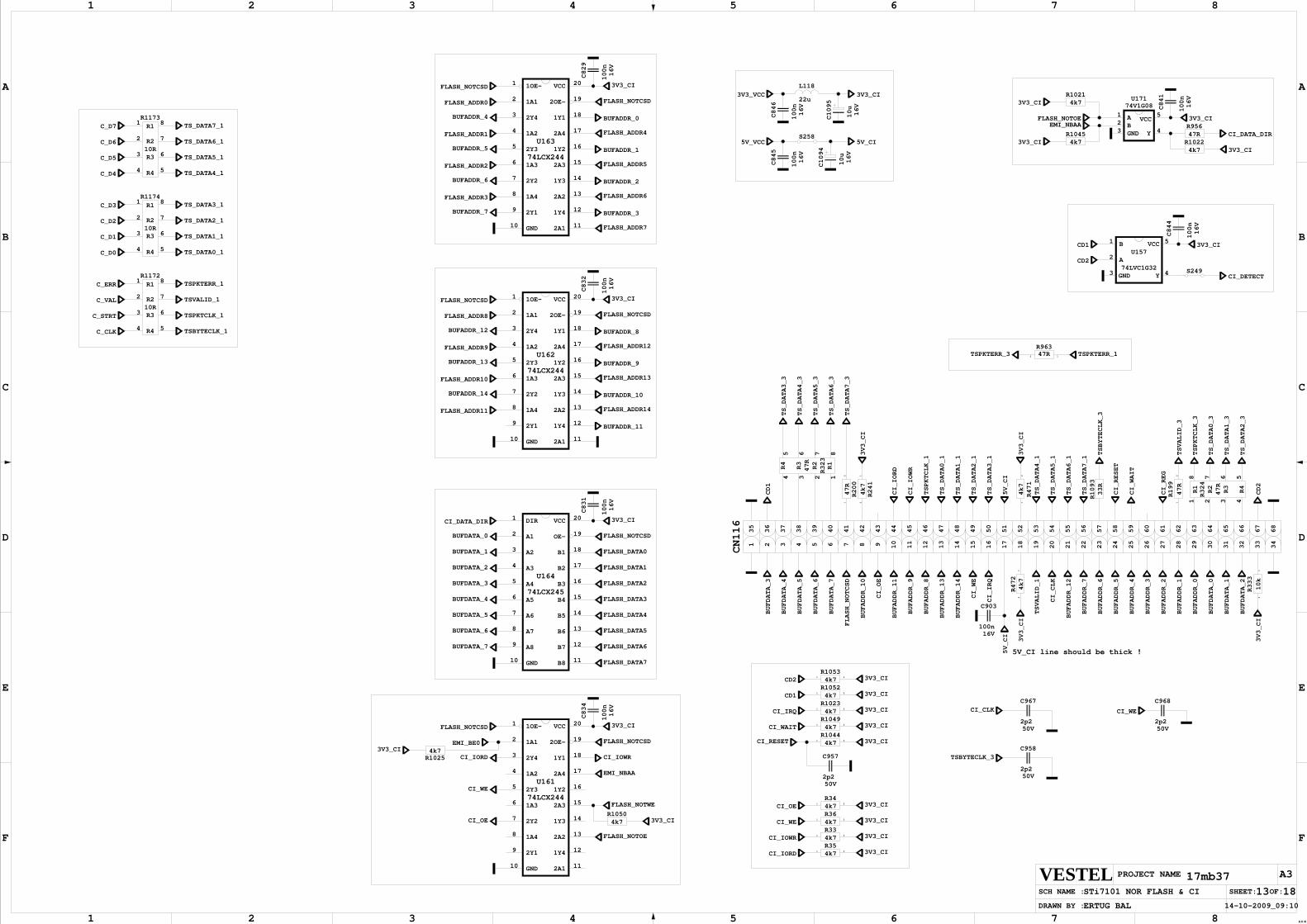
CI_OE
16V
10u
C1094
CI_IOWR
EMI_NBAA
CI_WE
CI_IOWR
CI_IORD 3V3_CI
3V3_CI
3V3_CI
3V3_CIR344k7
21
4k7R36
21
R334k7
21
4k7R35
21
74LVC1G32
U157
5
43
2
1 B
A
GND Y
VCC
16V100n
C903
CI_WE
STi7101 NOR FLASH & CI
ERTUG BAL
17mb371813
87654321
A
B
C
D
E
F
AX M
1 2 3 4 5 6 7 8
A
B
C
D
E
F
OF:
A3PROJECT NAME :VESTELSCH NAME :
DRAWN BY :
SHEET:
14-10-2009_09:10
74LCX244
U163
20
19
18
17
16
15
14
13
12
1110
9
8
7
6
5
4
3
2
1 1OE-
1A1
2Y4
1A2
2Y3
1A3
2Y2
1A4
2Y1
GND 2A1
1Y4
2A2
1Y3
2A3
1Y2
2A4
1Y1
2OE-
VCC
74LCX244
U161
20
19
18
17
16
15
14
13
12
1110
9
8
7
6
5
4
3
2
1 1OE-
1A1
2Y4
1A2
2Y3
1A3
2Y2
1A4
2Y1
GND 2A1
1Y4
2A2
1Y3
2A3
1Y2
2A4
1Y1
2OE-
VCC
74LCX244
U162
20
19
18
17
16
15
14
13
12
1110
9
8
7
6
5
4
3
2
1 1OE-
1A1
2Y4
1A2
2Y3
1A3
2Y2
1A4
2Y1
GND 2A1
1Y4
2A2
1Y3
2A3
1Y2
2A4
1Y1
2OE-
VCC
CI_IRQR10234k7
21
3V3_CI
BUFADDR_0
3V3_CI
74LCX245
U164
20
19
18
17
16
15
14
13
12
1110
9
8
7
6
5
4
3
2
1 DIR
A1
A2
A3
A4
A5
A6
A7
A8
GND B8
B7
B6
B5
B4
B3
B2
B1
OE-
VCC
16V
100n
C829
16V
100n
C832
16V
100n
C831
3V3_CI
16V
100n
C834
3V3_CI
FLASH_ADDR7
FLASH_ADDR6
FLASH_ADDR5
FLASH_ADDR4
FLASH_NOTCSD
BUFADDR_1
BUFADDR_2
BUFADDR_3
R323
47R
87654 3 2 1
R2
R3
R1
R4
10k
R333
21
47R
R324
8 7 6 54321
R2
R3
R1
R4
47R
R199
21
TSBYTECLK_3
CI_RESET
4k7
R472
21
4k7
R471
21
R200
47R
21
CN116
1 2 3 4 5 6 7 8 9 10
11
12
13
14
15
16
17
18
19
20
21
22
23
24
25
26
27
28
29
30
31
32
33
34
35
36
37
38
39
40
41
42
43
44
45
46
47
48
49
50
51
52
53
54
55
56
57
58
59
60
61
62
63
64
65
66
67
68
CI_CLK
3V3_CI
5V_CI
CI_IRQ
3V3_CI
5V_CI
R241
4k7
21
3V3_CI
TS_DATA7_3
TS_DATA6_3
TS_DATA5_3
TS_DATA4_3
TS_DATA3_3
3V3_CI
BUFADDR_12
TSVALID_1
3V3_CI
TSBYTECLK_3
TSVALID_3
TSPKTCLK_3
BUFDATA_3
4k7R1044
21
TS_DATA3_1
TSPKTCLK_1
TS_DATA0_3
TS_DATA1_3
TS_DATA2_3
TS_DATA1_1
TS_DATA0_1
TS_DATA2_1
TS_DATA4_1
TS_DATA5_1
TS_DATA6_1
TS_DATA7_1
CI_REG
CI_RESET
CI_IOWR
CI_WAIT
C958
2p2 50V
CD1
FLASH_NOTCSD
BUFDATA_6
BUFADDR_9
BUFDATA_2
CI_IORD
BUFDATA_0
BUFADDR_1
BUFADDR_3
BUFADDR_7
BUFDATA_1
BUFADDR_0
BUFADDR_2
BUFADDR_4
BUFADDR_6
CI_WE
BUFADDR_13
CI_OE
BUFDATA_4
BUFADDR_14
BUFADDR_8
BUFADDR_11
BUFADDR_10
BUFDATA_7
BUFDATA_5
BUFADDR_5
FLASH_NOTCSD
FLASH_NOTCSD
FLASH_NOTCSD
FLASH_NOTCSD
FLASH_NOTCSD
BUFADDR_7
FLASH_ADDR3
FLASH_ADDR2
FLASH_ADDR0
FLASH_ADDR1
BUFADDR_6
BUFADDR_5
BUFADDR_4
FLASH_ADDR14
BUFADDR_11
BUFADDR_8
BUFADDR_14
FLASH_ADDR13
FLASH_ADDR12
BUFADDR_9
BUFADDR_10
FLASH_ADDR10
FLASH_ADDR9
FLASH_ADDR8
FLASH_ADDR11
BUFDATA_0
BUFADDR_13
BUFADDR_12
BUFDATA_1
BUFDATA_2
BUFDATA_3
BUFDATA_4
BUFDATA_5
BUFDATA_6
BUFDATA_7
CI_DATA_DIR
FLASH_NOTCSD
FLASH_DATA0
FLASH_DATA1
FLASH_DATA4
FLASH_DATA3
FLASH_DATA2
FLASH_DATA7
FLASH_DATA6
FLASH_DATA5
FLASH_NOTOE
FLASH_NOTWE
4k7R1050
3V3_CI
EMI_BE0
CI_OE
CI_IORD4k7
R1025
3V3_CI
CI_WE
74V1G08U171
5
4321 A
BGND Y
VCCFLASH_NOTOEEMI_NBAA
3V3_CI
3V3_CI
4k7R1021
4k7R1045
3V3_CI
16V
100n
C841
47RR956
CI_DATA_DIR
4k7R1022
3V3_CI
3V3_CI3V3_VCC
C1095
10u
16V
22u
L118
50V2p2
C968
5V_VCC 5V_CIS258
16V
100n
C846
16V
100n
C845
CD1
CD2
16V
100n
C844
3V3_CI
CI_DETECTS249
3V3_CI
50V2p2
C957
CI_WAIT 3V3_CI4k7R1049
21
CD2
33R
R1093
50V2p2
C967
CI_CLK
10R
R11738
7
6
54
3
2
1
R2
R3
R1
R4
10R
R11748
7
6
54
3
2
1
R2
R3
R1
R4
10R
R11728
7
6
54
3
2
1
R2
R3
R1
R4
C_D7 TS_DATA7_1
C_D6
C_D5
C_D4
C_D3
C_D2
C_D1
C_D0
TS_DATA6_1
TS_DATA5_1
TS_DATA4_1
TS_DATA3_1
TS_DATA2_1
TS_DATA1_1
TS_DATA0_1
C_CLK
C_STRT
C_VAL
C_ERR
TSBYTECLK_1
TSPKTCLK_1
TSVALID_1
TSPKTERR_1
R96347R2 1 TSPKTERR_1TSPKTERR_3
3V3_CI4k7R1052
21
CD1
CD2 3V3_CIR10534k7
21
5V_CI line should be thick !
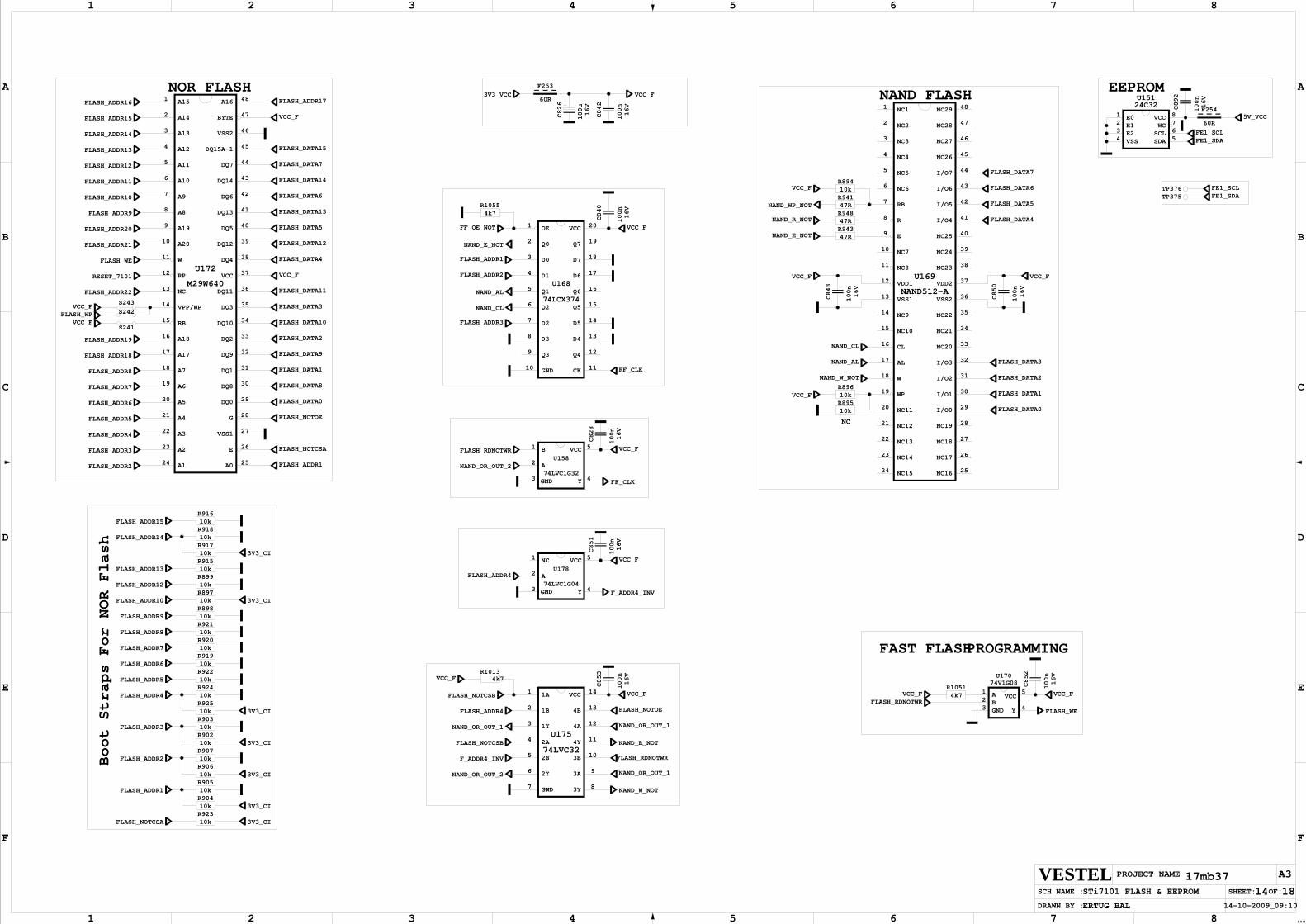
3V3_CI
3V3_CI
3V3_CI
3V3_CI
3V3_CI
3V3_CI
FE1_SDAFE1_SCLTP376
TP375
FLASH_WP S242
VCC_F
16V
100n
C828
47RR941
3V3_CI
FLASH_NOTCSA 10kR923
STi7101 FLASH & EEPROM
ERTUG BAL
17mb371814
87654321
A
B
C
D
E
F
AX M
1 2 3 4 5 6 7 8
A
B
C
D
E
F
OF:
A3PROJECT NAME :VESTELSCH NAME :
DRAWN BY :
SHEET:
14-10-2009_09:10
FF_CLK
74LVC1G32
U158
5
43
2
1 B
A
GND Y
VCC
74LCX374
U168
20
19
18
17
16
15
14
13
12
1110
9
8
7
6
5
4
3
2
1 OE
Q0
D0
D1
Q1
Q2
D2
D3
Q3
GND CK
Q4
D4
D5
Q5
Q6
D6
D7
Q7
VCC
NAND512-A
U169
48
47
46
45
44
43
42
41
40
39
38
37
36
35
34
33
32
31
30
29
28
27
26
2524
23
22
21
20
19
18
17
16
15
14
13
12
11
10
9
8
7
6
5
4
3
2
1 NC1
NC2
NC3
NC4
NC5
NC6
RB
R
E
NC7
NC8
VDD1
VSS1
NC9
NC10
CL
AL
W
WP
NC11
NC12
NC13
NC14
NC15 NC16
NC17
NC18
NC19
I/O0
I/O1
I/O2
I/O3
NC20
NC21
NC22
VSS2
VDD2
NC23
NC24
NC25
I/O4
I/O5
I/O6
I/O7
NC26
NC27
NC28
NC29
FE1_SDAFE1_SCL
C892
100n
16V
5V_VCC
24C32U151
78
654
321 E0
E1E2VSS SDA
SCL
VCCWC
FLASH_ADDR1 10kR905
10kR904
FLASH_ADDR2
FLASH_ADDR3
FLASH_ADDR4
FLASH_ADDR5
10kR907
10kR906
10kR903
10kR902
10kR925
FLASH_ADDR6
FLASH_ADDR7
FLASH_ADDR8
FLASH_ADDR9
FLASH_ADDR10
FLASH_ADDR12
FLASH_ADDR13
FLASH_ADDR14
FLASH_ADDR15
10kR922
10kR924
10kR920
10kR919
10kR898
10kR921
10kR899
10kR91810kR916
10kR897
10kR917
10kR915
FLASH_ADDR1
FLASH_NOTCSA
FLASH_NOTOE
VCC_F
VCC_F3V3_VCC
16V
100n
C842
FLASH_ADDR22
RESET_7101
FLASH_WE
FLASH_ADDR21
FLASH_ADDR19
FLASH_ADDR18
FLASH_ADDR8
FLASH_ADDR7
FLASH_ADDR6
FLASH_ADDR5
FLASH_ADDR4
FLASH_ADDR3
FLASH_DATA0
FLASH_DATA8
FLASH_DATA1
FLASH_DATA9
FLASH_DATA2
FLASH_DATA10
FLASH_DATA3
FLASH_DATA11
FLASH_DATA4
FLASH_DATA12
FLASH_DATA5
FLASH_DATA13
FLASH_DATA6
FLASH_DATA14
FLASH_DATA7
FLASH_DATA15
VCC_F
FLASH_ADDR11
FLASH_ADDR10
FLASH_ADDR9
FLASH_ADDR20
FLASH_ADDR12
FLASH_ADDR13
FLASH_ADDR17
FLASH_ADDR2
FLASH_ADDR14
FLASH_ADDR15
FLASH_ADDR16
M29W640
U172
48
47
46
45
44
43
42
41
40
39
38
37
36
35
34
33
32
31
30
29
28
27
26
2524
23
22
21
20
19
18
17
16
15
14
13
12
11
10
9
8
7
6
5
4
3
2
1 A15
A14
A13
A12
A11
A10
A9
A8
A19
A20
W
RP
NC
VPP/WP
RB
A18
A17
A7
A6
A5
A4
A3
A2
A1 A0
E
VSS1
G
DQ0
DQ8
DQ1
DQ9
DQ2
DQ10
DQ3
DQ11
VCC
DQ4
DQ12
DQ5
DQ13
DQ6
DQ14
DQ7
DQ15A-1
VSS2
BYTE
A16
VCC_F
S241
S243
VCC_F
NAND_CL
NAND_R_NOT
NAND_WP_NOT
10kR894
R94847R
NAND_E_NOT 47RR943
VCC_FFLASH_RDNOTWR
NAND_OR_OUT_2
FF_CLK
VCC_F
C840
100n
16V
NAND_AL
FF_OE_NOT
4k7R1055
FLASH_ADDR2
FLASH_ADDR3
FLASH_ADDR1
NAND_CL
NAND_E_NOT
VCC_F
60R
F253
16V
100n
C843
NAND_AL
NAND_W_NOT
R89610k
10kR895
VCC_F
FLASH_DATA0
FLASH_DATA1
FLASH_DATA2
FLASH_DATA3
FLASH_DATA6
74LVC32
U175
1
2
3
4
5
6
7
14
13
12
11
10
9
83Y
3A
3B
4Y
4A
4B
VCC
GND
2Y
2B
2A
1Y
1B
1A
FLASH_DATA5
FLASH_DATA4
FLASH_DATA7
VCC_F
C850
100n
16V
16V
100u
C826
VCC_F
C853
100n
16V
FLASH_NOTCSB
FLASH_ADDR4
FLASH_NOTCSB
F_ADDR4_INV
FLASH_NOTOE
NAND_OR_OUT_1
FLASH_RDNOTWR
NAND_OR_OUT_1
NAND_R_NOT
74V1G08U170
5
4321 A
BGND Y
VCCVCC_FFLASH_RDNOTWR
FLASH_WE
VCC_F
16V
100n
C852
4k7R1051
74LVC1G04
U178
5
43
2
1 NC
A
GND Y
VCC
C851
100n
16V
VCC_F
FLASH_ADDR4
F_ADDR4_INV
NAND_W_NOT
NAND_OR_OUT_1
NAND_OR_OUT_2
4k7R1013
VCC_F
60R
F254
NAND FLASHNOR FLASH
NC
EEPROM
FAST FLASHPROGRAMMING
Boot Straps For NOR Flash
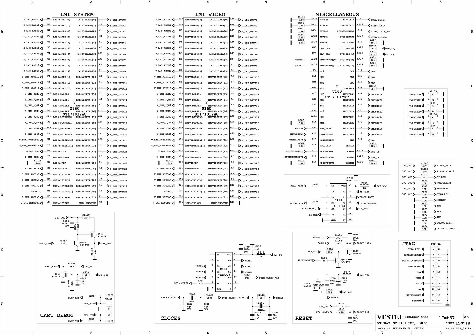
TMDSTX0P
TMDSTX1P
TMDSTX1N
TMDSTX2P
TMDSTX2N
TMDSTXCP
TMDSTXCN
TMDSTXCP
TMDSTXCN
TMDSTX2P
TMDSTX2N
TMDSTX1P
TMDSTX1N
TMDSTX0P
TMDSTX0N
27k
R1072
C94033p 50V
16V100n C854
BC847BQ167
Q165BC847B
Q168BC847B
UART_TXD
RXD_CON
UART_RXDR10663k3 3V3_VCC
R10334k7UART_TXD
R9701k
R1067
3k3
CN135
3
2
1
75RR1119
2k2
R1129
TXD_CON
RXD_CON
UART_RXD
TXD_CON
12V_VCC
S245
S238TP365
TP366
LM809U159
2
3
1
GNDVCC
RST
PONRST
3k9R1071
3V3_VCC
F24721
3V3_VCC
16V100u C821
10V100n C738
NOTJTAGRST 1kR998
BC847BQ169
10kR870
Q166BC847B
3V3_VCC
RESET_7101
C737100n 10V
10kR886
33RR185
2 1 RESET_DVB
10V100n C2512
1
10kR375
21
3V3_VCC
DVB_RESET
STi7101 LMI, MISC
HUSEYIN E. CETIN
17mb371815
87654321
A
B
C
D
E
F
AX M
1 2 3 4 5 6 7 8
A
B
C
D
E
F
OF:
A3PROJECT NAME :VESTELSCH NAME :
DRAWN BY :
SHEET:
14-10-2009_09:10
S_LMI_DATA0
S_LMI_DATA1
STI7101YWC
U160
R2
P1
P2
N1
N2
M1
M2
L1
L2
AG2
AG1
AF2
AF1
AE2
AE1
AD2
AD1
H1
H2
G1
G2
F1
F2
E1
E2
AA2
AA1
Y2
Y1
W2
W1
V2
V1
J5
K5
M5
L4
U2
J4
H5
R1
Y5
U1
L5
K4
K1
AC2
J2
AB1
K2
AC1
J1
AB2
T4
T5
P4
U5
W4
W5
V4
V5
U4
P5
N4
N5
M4 LMISYSADD[0]
LMISYSADD[1]
LMISYSADD[2]
LMISYSADD[3]
LMISYSADD[4]
LMISYSADD[5]
LMISYSADD[6]
LMISYSADD[7]
LMISYSADD[8]
LMISYSADD[9]
LMISYSADD[10]
LMISYSADD[11]
LMISYSADD[12]
LMIS_DMASK0
LMIS_DMASK1
LMIS_DMASK2
LMIS_DMASK3
LMIS_DSTROBE0
LMIS_DSTROBE1
LMIS_DSTROBE2
LMIS_DSTROBE3
LMISYSBKSEL[0]
LMISYSBKSEL[1]
LMISYSCLK
LMISYSCLKEN
LMISYSREF
LMISYSVREF
NOTLMISYSCAS
NOTLMISYSCLK
NOTLMISYSCS[0]
NOTLMISYSCS[1]
NOTLMISYSRAS
NOTLMISYSWE
LMISYSDATA[0]
LMISYSDATA[1]
LMISYSDATA[2]
LMISYSDATA[3]
LMISYSDATA[4]
LMISYSDATA[5]
LMISYSDATA[6]
LMISYSDATA[7]
LMISYSDATA[8]
LMISYSDATA[9]
LMISYSDATA[10]
LMISYSDATA[11]
LMISYSDATA[12]
LMISYSDATA[13]
LMISYSDATA[14]
LMISYSDATA[15]
LMISYSDATA[16]
LMISYSDATA[17]
LMISYSDATA[18]
LMISYSDATA[19]
LMISYSDATA[20]
LMISYSDATA[21]
LMISYSDATA[22]
LMISYSDATA[23]
LMISYSDATA[24]
LMISYSDATA[25]
LMISYSDATA[26]
LMISYSDATA[27]
LMISYSDATA[28]
LMISYSDATA[29]
LMISYSDATA[30]
LMISYSDATA[31]
LMIS_GNDCOMP
3
S_LMI_DATA2
S_LMI_DATA3
S_LMI_DATA7
S_LMI_DATA6
S_LMI_DATA5
S_LMI_DATA4
S_LMI_DATA11
S_LMI_DATA10
S_LMI_DATA9
S_LMI_DATA8
S_LMI_DATA15
S_LMI_DATA14
S_LMI_DATA13
S_LMI_DATA12
S_LMI_DATA19
S_LMI_DATA18
S_LMI_DATA17
S_LMI_DATA16
S_LMI_DATA23
S_LMI_DATA22
S_LMI_DATA21
S_LMI_DATA20
S_LMI_DATA27
S_LMI_DATA26
S_LMI_DATA25
S_LMI_DATA24
S_LMI_DATA31
S_LMI_DATA30
S_LMI_DATA29
S_LMI_DATA28
S_LMI_ADDR0
S_LMI_ADDR1
S_LMI_ADDR2
S_LMI_ADDR3
S_LMI_ADDR7
S_LMI_ADDR6
S_LMI_ADDR5
S_LMI_ADDR4
S_LMI_ADDR11
S_LMI_ADDR10
S_LMI_ADDR9
S_LMI_ADDR8
S_LMI_ADDR12
1MR1143
S_LMI_DQM0
S_LMI_DQM1
S_LMI_DQM2
S_LMI_DQM3
S_LMI_DQS3
S_LMI_DQS2
S_LMI_DQS1
S_LMI_DQS0
S_LMI_NOTBANK0
S_LMI_NOTBANK1
S_LMI_CKEN
120kR1150
S_LMI_CLK
S_LMI_VREF
S_LMI_NOTCLK
S_LMI_NOTCAS
S_LMI_NOTCS0
TP251
S_LMI_NOTRAS
S_LMI_RDNOTWR V_LMI_RDNOTWR
V_LMI_NOTRAS
V_LMI_NOTCAS
TP250
V_LMI_NOTCS0
V_LMI_NOTCLK
V_LMI_VREF
V_LMI_CKEN
R1151120k
V_LMI_CLK
V_LMI_NOTBANK1
V_LMI_NOTBANK0
V_LMI_DQS3
V_LMI_DQS2
V_LMI_DQS1
V_LMI_DQS0
V_LMI_DQM3
V_LMI_DQM2
V_LMI_DQM1
V_LMI_DQM0
V_LMI_ADDR12
V_LMI_ADDR11
V_LMI_ADDR10
V_LMI_ADDR9
V_LMI_ADDR8
V_LMI_ADDR7
V_LMI_ADDR6
V_LMI_ADDR5
V_LMI_ADDR4
V_LMI_ADDR3
V_LMI_ADDR2
V_LMI_ADDR1
V_LMI_ADDR0 V_LMI_DATA0
V_LMI_DATA31
V_LMI_DATA30
V_LMI_DATA29
V_LMI_DATA28
V_LMI_DATA27
XTAL1 XTAL2
50V22p C923
V_LMI_DATA26
V_LMI_DATA25
V_LMI_DATA24
V_LMI_DATA23
R88010k
10kR888
R88510k
V_LMI_DATA22
V_LMI_DATA21
V_LMI_DATA20
V_LMI_DATA19
V_LMI_DATA18
V_LMI_DATA17
V_LMI_DATA16
V_LMI_DATA15
V_LMI_DATA14
V_LMI_DATA13
V_LMI_DATA12
V_LMI_DATA11
V_LMI_DATA10
V_LMI_DATA9
V_LMI_DATA8
V_LMI_DATA7
V_LMI_DATA6
V_LMI_DATA5
V_LMI_DATA4
V_LMI_DATA3
V_LMI_DATA2
V_LMI_DATA1
STI7101YWC
U160
B11
A11
A10
B10
A9
B9
A8
B8
A7
B23
A23
B22
A22
B21
A21
B20
A20
B5
A4
B4
A3
B3
A2
B2
A1
B17
A17
B16
A16
B15
A15
B14
A14
E15
E14
E11
D11
B13
D15
C11
B12
D13
A13
E13
D14
B7
B19
A5
A18
A6
A19
B6
B18
D7
E8
D8
E7
D4
E5
D5
E6
D6
D9
E9
D10
E10 LMIVIDADD[0]
LMIVIDADD[1]
LMIVIDADD[2]
LMIVIDADD[3]
LMIVIDADD[4]
LMIVIDADD[5]
LMIVIDADD[6]
LMIVIDADD[7]
LMIVIDADD[8]
LMIVIDADD[9]
LMIVIDADD[10]
LMIVIDADD[11]
LMIVIDADD[12]
LMIV_DMASK0
LMIV_DMASK1
LMIV_DMASK2
LMIV_DMASK3
LMIV_DSTROBE0
LMIV_DSTROBE1
LMIV_DSTROBE2
LMIV_DSTROBE3
LMIVIDBKSEL[0]
LMIVIDBKSEL[1]
LMIVIDCLK
LMIVIDCLKEN
LMIVIDREF
LMIVIDVREF
NOTLMIVIDCAS
NOTLMIVIDCLK
NOTLMIVIDCS[0]
NOTLMIVIDCS[1]
NOTLMIVIDRAS
NOTLMIVIDWE
LMIVIDDATA[0]
LMIVIDDATA[1]
LMIVIDDATA[2]
LMIVIDDATA[3]
LMIVIDDATA[4]
LMIVIDDATA[5]
LMIVIDDATA[6]
LMIVIDDATA[7]
LMIVIDDATA[8]
LMIVIDDATA[9]
LMIVIDDATA[10]
LMIVIDDATA[11]
LMIVIDDATA[12]
LMIVIDDATA[13]
LMIVIDDATA[14]
LMIVIDDATA[15]
LMIVIDDATA[16]
LMIVIDDATA[17]
LMIVIDDATA[18]
LMIVIDDATA[19]
LMIVIDDATA[20]
LMIVIDDATA[21]
LMIVIDDATA[22]
LMIVIDDATA[23]
LMIVIDDATA[24]
LMIVIDDATA[25]
LMIVIDDATA[26]
LMIVIDDATA[27]
LMIVIDDATA[28]
LMIVIDDATA[29]
LMIVIDDATA[30]
LMIVIDDATA[31]
LMIV_GNDCOMP
4
STI7101YWC
U160
AM25
AN25
AP25
E18
E21
U33
U34
P33
P34
R33
R34
T33
T34
T32
E22
D22
D21
AK28
AK27
AK26
AK25
E17
AN27
E27
AP27
C1
E19
D18
D17
D16
D19
E20
D20
E16
AM31
L31
C30
A29
AP9
AN9
AM5
AL6
G5
AL22
AN22
AP5
AN5
AN30
AP30
AN31
AP31
AM30 ATAREF
ATARXN
ATARXP
ATATXN
ATATXP
DAA_C1A
DAA_C2A
EMIDMAREQ[0]
EMIDMAREQ[1]
NC1
NC2
NC3
NC4
NC5
NC6
NC7
NC8
NC9
NMI
NOT_TRST
NOTASEBRK
NOTRESETIN
RTCCLKIN
TRIGGERIN
TRIGGEROUT
WDOGRSTOUT
SYSACLKIN
SYSBCLKIN
SYSBCLKINALT
SYSBCLKOSC
SYSCLKOUT
SYSITRQ[0]
SYSITRQ[1]
SYSITRQ[2]
SYSITRQ[3]
TCK
TDI
TDO
TMDSREF
TMDSTX0N
TMDSTX0P
TMDSTX1N
TMDSTX1P
TMDSTX2N
TMDSTX2P
TMDSTXCN
TMDSTXCP
TMS
TMUCLK
USBDM
USBDP
USBREF
5
SYSA_CLKIN
SYSB_CLKIN_ALT
SYSB_CLKIN
SYSB_CLKOSC
10kR887
10kR879
10kR882
TDO
TMDSTX0N
100RR1076
DVB_IRQ
47RR957
CI_IRQ
TCK
75RR1124
TDI
10k
R11558
7
6
54
3
2
1
R2
R3
R1
R4
10k
R11548
7
6
54
3
2
1
R2
R3
R1
R4
TMS
10kR884
USB_DN
USB_DP
12kR1005
470RR1130
TP262
TP261
R88310k
NOTRST
NOTASEBRK
RESET_7101
10kR881
DCUTRIGGERIN
DCUTRIGGEROUT
R87810k
3k3R1065
PONRST
R10683k3RESET_DVB
47RR966
SYSB_CLKIN_ALT
XTAL2
XTAL2
XTAL1
2V5_ST
10u C992
10V100n C739
F274
1k
R96547RSYSA_CLKIN
XTAL2
XTAL2
XTAL1
30MHz
X106
C92422p 50V
X107
30MHzC92122p 50V
SYSB_CLKOSC SYSB_CLKIN120RR1169
50V22p C922
JTAG_PIN1
NOTASEBRK
S231
S232
TSBYTECLK_1
CI_CLK
CI_WAIT
100n C742
F258
1k3V3_VCC
FLASH_ADDR18
FLASH_WAIT
CI_REG
4k7R1054
3V3_VCC FLASH_ADDR18
CI_REGR10484k73V3_VCC
FLASH_WAITR10204k73V3_VCC
10kR871
3V3_VCC NOTJTAGRST
NOTASEBRKR90110k3V3_VCC
JTAG_PIN110kR900
3V3_VCC
R87510k NOTRST
TDI10kR877
TCKR87310k
TMS10kR872
DCUTRIGGERINR87610k
DCUTRIGGEROUT10kR874
NOTRST
TDO
NOTJTAGRST
TDI
TCK
TMS
NOTASEBRK
DCUTRIGGEROUT
DCUTRIGGERIN
JTAG_PIN1
74HCU04
U181
1
2
3
4
5
6
7
14
13
12
11
10
9
84Y
4A
5Y
5A
6Y
6A
VCC
GND
3Y
3A
2Y
2A
1Y
1A
74HCU04
U180
1
2
3
4
5
6
7
14
13
12
11
10
9
84Y
4A
5Y
5A
6Y
6A
VCC
GND
3Y
3A
2Y
2A
1Y
1A
CN136
2019
1817
1615
1413
1211
109
87
65
43
21
UART DEBUG
LMI SYSTEM MISCELLANEOUSLMI VIDEO
CLOCKS RESET
JTAG
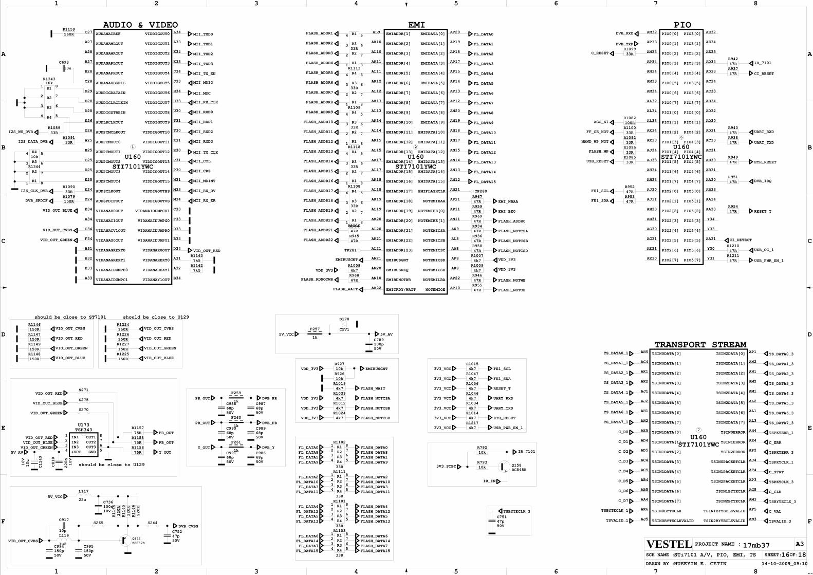
USB_PWR_EN_1R12174k73V3_VCC
VID_OUT_BLUE
VID_OUT_RED
VID_OUT_GREEN
R1226150R
150RR1227
S271
S275
S270
VID_OUT_RED
VID_OUT_BLUE
VID_OUT_GREEN
33RR1089
I2S_WS_DVB
16V
10u
C1149
R1225150R
150RR1224
VID_OUT_CVBS
R121047R
STI7101YWC
U160
Y31
Y30
AA31
Y33
Y34
AA33
AA34
AB33
AA30
AB31
AB30
AC31
AC30
AD31
AD30
AD32
AB34
AC33
AC34
AD33
AD34
AE33
AE34
AE32
AE30
AE31
AG31
AG30
AH31
AH30
AJ31
AJ30
AH33
AH34
AJ33
AJ34
AK33
AK34
AL33
AL34
AL32
AM34
AM33
AN34
AP34
AN33
AP33
AM32 PIO0[0]
PIO0[1]
PIO0[2]
PIO0[3]
PIO0[4]
PIO0[5]
PIO0[6]
PIO0[7]
PIO1[0]
PIO1[1]
PIO1[2]
PIO1[3]
PIO1[4]
PIO1[5]
PIO1[6]
PIO1[7]
PIO2[0]
PIO2[1]
PIO2[2]
PIO2[3]
PIO2[4]
PIO2[5]
PIO2[6]
PIO2[7]
PIO3[0]
PIO3[1]
PIO3[2]
PIO3[3]
PIO3[4]
PIO3[5]
PIO3[6]
PIO3[7]
PIO4[0]
PIO4[1]
PIO4[2]
PIO4[3]
PIO4[4]
PIO4[5]
PIO4[6]
PIO4[7]
PIO5[0]
PIO5[1]
PIO5[2]
PIO5[3]
PIO5[4]
PIO5[5]
PIO5[6]
PIO5[7]
6
VID_OUT_GREEN
VID_OUT_CVBS
IR_7101
IR_IN
3V3_STBY
10kR792
10kR793
BC848BQ158
R1146150R
50V47p C751
TSBYTECLK_3
STi7101 A/V, PIO, EMI, TS
HUSEYIN E. CETIN
17mb371816
87654321
A
B
C
D
E
F
AX M
1 2 3 4 5 6 7 8
A
B
C
D
E
F
OF:
A3PROJECT NAME :VESTELSCH NAME :
DRAWN BY :
SHEET:
14-10-2009_09:10
TSH343U173
5
876
4321 IN1
IN2IN3+VCC
OUT3OUT2OUT1
GND
50V68p C988
F259
1kC98768p 50V
DVB_PR
50V100p C789
PR_OUT
PB_OUT
C99068p 50V
1k
F260
50V68p C989
DVB_PB
DVB_Y
C98668p 50V
F261
1k
50V68p C991
Y_OUT
50V47p C752
C_VAL
TSBYTECLK_3
C_CLK
TSPKTCLK_3
C_STRT
TSPKTCLK_1
TSPKTERR_3
C_ERR
TSPKTERR_1
TS_DATA7_3
TS_DATA6_3
TS_DATA5_3
TS_DATA4_3
TS_DATA3_3
TS_DATA2_3
TS_DATA1_3
10V
220n
C810
VID_OUT_REDVID_OUT_BLUEVID_OUT_GREEN
5V_AV
1k
F257
5V_VCC 5V_AV
TS_DATA0_3
PR_OUT
PB_OUT
Y_OUT
75RR1157
R115875R
75RR1156
TSVALID_3TSVALID_1
TSBYTECLK_1
C_D7
C_D6
C_D5
C_D4
C_D3
C_D2
C_D1
C_D0
TS_DATA7_1
TS_DATA6_1
TS_DATA5_1
TS_DATA4_1
TS_DATA3_1
TS_DATA2_1
TS_DATA1_1
TS_DATA0_1
STI7101YWCU160
AN3
AF5
AM3
AG5
AP3
AF4
AJ4
AP2
AE4
AH4
AL3
AL1
AL2
AM1
AM2
AN1
AN2
AP1
AJ5
AK6
AA4
AB5
AB4
AC5
AC4
AD5
AD4
AE5
AH2
AH1
AJ2
AJ1
AK2
AK1
AG4
AH5 TSIN0DATA[0]
TSIN0DATA[1]
TSIN0DATA[2]
TSIN0DATA[3]
TSIN0DATA[4]
TSIN0DATA[5]
TSIN0DATA[6]
TSIN0DATA[7]
TSIN1DATA[0]
TSIN1DATA[1]
TSIN1DATA[2]
TSIN1DATA[3]
TSIN1DATA[4]
TSIN1DATA[5]
TSIN1DATA[6]
TSIN1DATA[7]
TSIN0BYTECLK
TSIN0BYTECLKVALID
TSIN2DATA[0]
TSIN2DATA[1]
TSIN2DATA[2]
TSIN2DATA[3]
TSIN2DATA[4]
TSIN2DATA[5]
TSIN2DATA[6]
TSIN2DATA[7]
TSIN0ERROR
TSIN1ERROR
TSIN2ERROR
TSIN0PACKETCLK
TSIN1PACKETCLK
TSIN2PACKETCLK
TSIN1BYTECLK
TSIN2BYTECLK
TSIN1BYTECLKVALID
TSIN2BYTECLKVALID
7
STI7101YWC
U160
C27
A27
A28
B27
B28
C28
D29
E28
D28
E26
D26
A25
B25
C25
D25
E25
E24
D24
E34
A34
C34
F34
B31
B32
E33
A33
L34
L33
K34
K33
J34
J33
H34
H33
U30
T31
T30
R31
R30
P31
P30
N31
M33
M34
C33
F33
D33
B33
D34
A31
A32
B34VIDANAY1OUT
VIDANAREXT1
VIDANAREXT0
VIDANAR0OUT
VIDANAIDUMPY1
VIDANAIDUMPR0
VIDANAIDUMPG0
VIDANAIDUMPCV1
VIDDIGOUTVS
VIDDIGOUTHS
VIDDIGOUT15
VIDDIGOUT14
VIDDIGOUT13
VIDDIGOUT12
VIDDIGOUT11
VIDDIGOUT10
VIDDIGOUT9
VIDDIGOUT8
VIDDIGOUT7
VIDDIGOUT6
VIDDIGOUT5
VIDDIGOUT4
VIDDIGOUT3
VIDDIGOUT2
VIDDIGOUT1
VIDDIGOUT0
VIDANAIDUMPC1
VIDANAIDUMPB0
VIDANAGREXT1
VIDANAGREXT0
VIDANAG0OUT
VIDANACV1OUT
VIDANAC1OUT
VIDANAB0OUT
AUDSPDIFOUT
AUDSCLKOUT
AUDPCMOUT4
AUDPCMOUT3
AUDPCMOUT2
AUDPCMOUT1
AUDPCMOUT0
AUDPCMCLKOUT
AUDLRCLKOUT
AUDDIGSTRBIN
AUDDIGLRCLKIN
AUDDIGDATAIN
AUDANAVBGFIL
AUDANAPROUT
AUDANAPLOUT
AUDANAMROUT
AUDANAMLOUT
AUDANAIREF
1
STI7101YWC
U160
AP10
AP22
AK8
AP8
AM8
AL8
AK9
AN11
AP11
AP21
AN21
AN12
AN13
AN14
AN15
AN17
AN18
AN19
AN20
AP12
AP13
AP14
AP15
AP17
AP18
AP19
AP20
AK22
AN10
AM20
AM21
AL21
AK21
AL20
AK20
AL19
AK19
AL18
AK18
AL17
AK17
AL15
AK15
AL14
AK14
AL13
AK13
AL12
AK12
AL11
AK11
AL10
AK10
AL9 EMIADDR[1]
EMIADDR[2]
EMIADDR[3]
EMIADDR[4]
EMIADDR[5]
EMIADDR[6]
EMIADDR[7]
EMIADDR[8]
EMIADDR[9]
EMIADDR[10]
EMIADDR[11]
EMIADDR[12]
EMIADDR[13]
EMIADDR[14]
EMIADDR[15]
EMIADDR[16]
EMIADDR[17]
EMIADDR[18]
EMIADDR[19]
EMIADDR[20]
EMIADDR[21]
EMIADDR[22]
EMIADDR[23]
EMIBUSGNT
EMIBUSREQ
EMIRDNOTWR
EMITRDY/WAIT
EMIDATA[0]
EMIDATA[1]
EMIDATA[2]
EMIDATA[3]
EMIDATA[4]
EMIDATA[5]
EMIDATA[6]
EMIDATA[7]
EMIDATA[8]
EMIDATA[9]
EMIDATA[10]
EMIDATA[11]
EMIDATA[12]
EMIDATA[13]
EMIDATA[14]
EMIDATA[15]
EMIFLASHCLK
NOTEMIBAA
NOTEMIBE[0]
NOTEMIBE[1]
NOTEMICSA
NOTEMICSB
NOTEMICSC
NOTEMICSD
NOTEMICSE
NOTEMILBA
NOTEMIOE
2
560RR1159
10u
C693
R1344
10k
8
7
6
54
3
2
1
R2
R3
R1
R4
R109033R
R109133R
VID_OUT_BLUE
DVB_SPDIF 100RR1079
150RR1148
VID_OUT_GREEN
VID_OUT_BLUE
I2S_DATA_DVB
I2S_CLK_DVB
VID_OUT_RED
R1149150R
150RR1147
VID_OUT_CVBS
VID_OUT_RED
7k5R1163
R11627k5
FL_DATA0
FL_DATA1
FL_DATA2
FL_DATA3
FL_DATA4
FL_DATA5
FL_DATA6
FL_DATA7
FL_DATA8
FL_DATA9
FL_DATA10
FL_DATA11
FL_DATA12
FL_DATA13
FL_DATA14
FL_DATA15
33R
R11138
7
6
54
3
2
1
R2
R3
R1
R4FLASH_ADDR1
FLASH_ADDR2
FLASH_ADDR3
FLASH_ADDR4
FLASH_ADDR8
FLASH_ADDR7
FLASH_ADDR6
FLASH_ADDR5
R1109
33R
8
7
6
54
3
2
1
R2
R3
R1
R4
33R
R11188
7
6
54
3
2
1
R2
R3
R1
R4
R1108
33R
8
7
6
54
3
2
1
R2
R3
R1
R4
33R
R11108
7
6
54
3
2
1
R2
R3
R1
R4
FLASH_ADDR16
FLASH_ADDR15
FLASH_ADDR14
FLASH_ADDR13
FLASH_ADDR12
FLASH_ADDR11
FLASH_ADDR10
FLASH_ADDR9
FLASH_ADDR20
FLASH_ADDR19
FLASH_ADDR18
FLASH_ADDR17
47RR944
47RR945
FLASH_ADDR21
FLASH_ADDR22
TP281
10kR927
10kR926
EMIBUSGNT
4k7R1008
VDD_3V3
EMIBUSGNTVDD_3V3
R96847RFLASH_RDNOTWR
R10194k7
FLASH_WAIT
FLASH_WAIT
TP280
R96747R EMI_NBAA
47RR959
EMI_BE0R96947R FLASH_ADDR0
47RR934
FLASH_NOTCSA
4k7R1039
FLASH_NOTCSAVDD_3V3
FLASH_NOTCSBR93647R
FLASH_NOTCSDR95847R
FLASH_NOTCSBR10124k7VDD_3V3
VDD_3V34k7R1007
VDD_3V3R10094k7
47RR946
FLASH_NOTWER95547R FLASH_NOTOE
33R
R110287654
321
R4R3R2R1FL_DATA0
FL_DATA8FL_DATA1FL_DATA9
FLASH_DATA0FLASH_DATA8FLASH_DATA1FLASH_DATA9
FLASH_DATA11FLASH_DATA3FLASH_DATA10FLASH_DATA2
FL_DATA11FL_DATA3
FL_DATA10FL_DATA2
R1111
33R
87654
321
R4R3R2R1
33R
R110187654
321
R4R3R2R1FL_DATA4
FL_DATA12FL_DATA5
FL_DATA13
FLASH_DATA4FLASH_DATA12FLASH_DATA5FLASH_DATA13
R1103
33R
87654
321
R4R3R2R1FL_DATA6
FL_DATA14FL_DATA7
FL_DATA15
FLASH_DATA6FLASH_DATA14FLASH_DATA7FLASH_DATA15
DVB_RXD
DVB_TXD
33RR1099
C_RESET
10kR1343
8
7
6
54
3
2
1
R2
R3
R1
R4AGC_S1 100R
R1082
47RR952
R95347R
FE1_SCL
FE1_SDA
4k7R1015
3V3_VCC FE1_SCL
3V3_VCCR10474k7 FE1_SDA
R94247R IR_7101
47RR937
CI_RESET
R94047R
47RR938
R95147R
UART_RXD
UART_TXD
DVB_IRQ
R10464k7
47RR954
RESET_T
3V3_VCC RESET_T4k7R1056
CI_DETECT
47RR1211
VID_OUT_CVBS
50V150p C9941u2
L11910p
C917
C995150p 50V
BC857BQ172
220R
R1165
R1166
220R
220R
R1164
10V100n C736
22u
L117
5V_VCC
S244DVB_CVBS
UART_RXD3V3_VCC
UART_TXD4k7R1034
3V3_VCC
R110033RFF_OE_NOT
33RR1092
NAND_WP_NOT
R109533RFLASH_WP
33RR1085
USB_RESET ETH_RESETR94947R
3V3_VCCR10144k7 ETH_RESET
USB_OC_1
USB_PWR_EN_1
VDD_3V3 4k7R1024
FLASH_NOTCSD
MII_TXD0
MII_RX_CLK
MII_TXD1
MII_TXD2
MII_TXD3
MII_TX_EN
MII_MDIO
MII_MDC
MII_RXD0
MII_RXD1
MII_RXD2
MII_RXD3
MII_TX_CLK
MII_COL
MII_CRS
MII_MDINT
MII_RX_DV
MII_RX_ER
S265
C5V1
D170
should be close to U129
should be close to U129should be close to ST7101
TRANSPORT STREAM
AUDIO & VIDEO EMI PIO
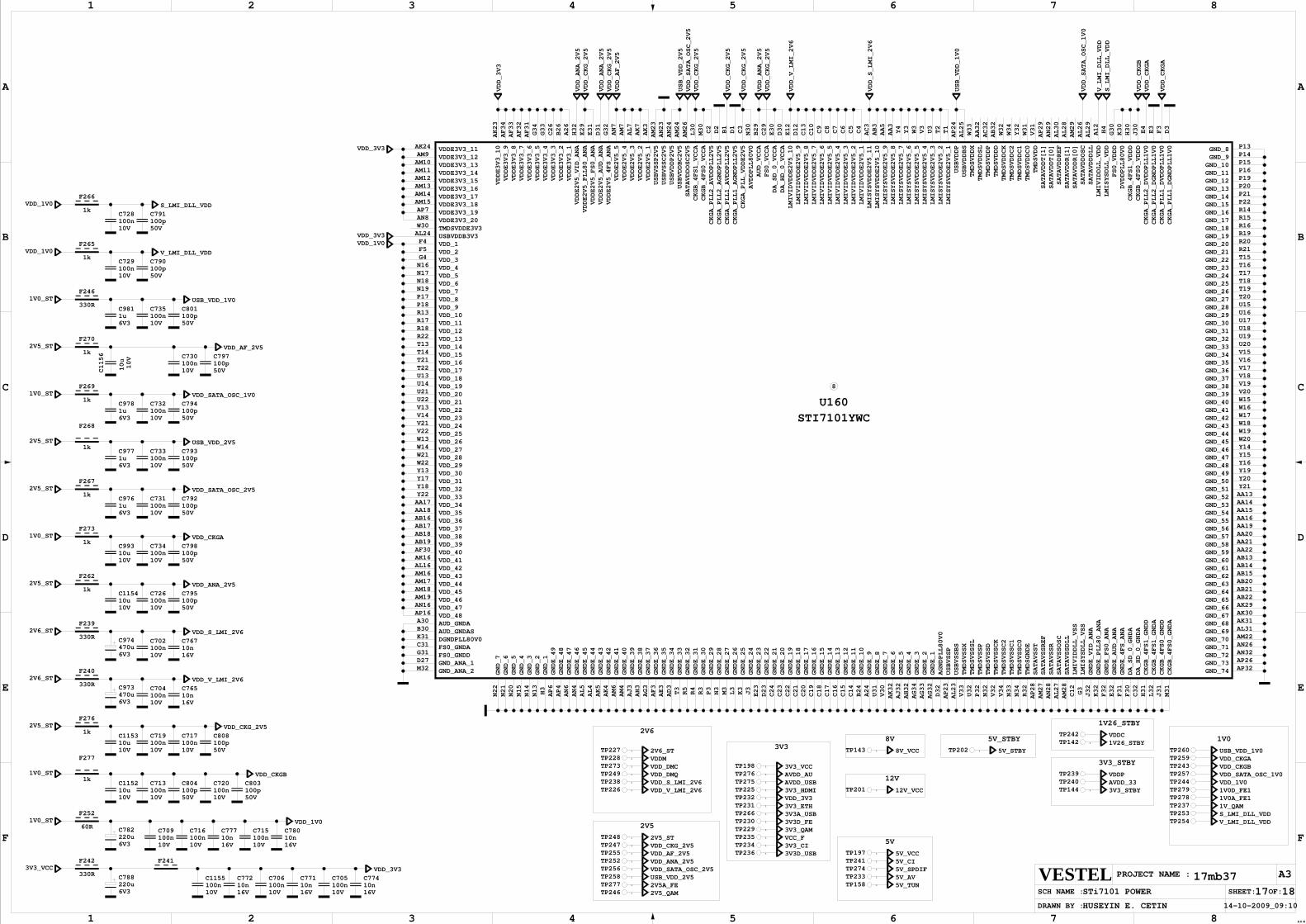
TP158 1
5V_STBY
12V_VCC 3V3_STBY
TP143 1
5V_VCC
3V3_VCC
C1153
10V10u
6V3220u C782
TP238 1
TP237
3V3D_USBTP236 1 TP197 1
5V_CI
10V
10u
C1156
STi7101 POWER
HUSEYIN E. CETIN
17 18
17mb37
87654321
A
B
C
D
E
F
AX M
1 2 3 4 5 6 7 8
A
B
C
D
E
F
OF:
A3PROJECT NAME :VESTELSCH NAME :
DRAWN BY :
SHEET:
14-10-2009_09:10
STI7101YWCU160
AP32AP26AN32AN26AM22AL31AK31AK30AK29AB22AB21AB20AB15AB14AB13AA22AA21AA20AA19AA16AA15AA14AA13Y21Y20Y19Y16Y15Y14W20W19W18W17W16W15V20V19V18V17V16V15U20U19U18U17U16U15T20T19T18T17T16T15R21R20R19R16R15R14P22P21P20P19P16P15P14P13
N22
N21
N20
N15
N14
N13
H3
AP6
AP4
AN6
AN4
AL5
AL4
AK5
AK4
AM6
AM4
AJ3
AH3
AG3
AF3
AE3
AD3
T3
R5
R4
R3
P3
N3
M3
L3
K3
J3
E23
D23
C24
C23
C22
C21
C20
C19
C18
C17
C16
C15
C14
B24
A24
U31
V30
AK32
AJ32
AH32
AG34
AG33
AG32
D32
AP23
AL23
V33
U32
P32
N32
V32
V34
N33
N34
R32
AP28
AM27
AN28
AL27
AM28
C12
G3
J32
K32
F32
E32
F31
F30
C32
H31
L32
J31
M31
M32D27G31C31K31B30A30AP16AN16AM19AM18AM17AM16AL16AK16AF30AB19AB18AB17AB16AA18AA17Y22Y18Y17Y13W22W21W14W13V22V21V14V13U22U21U14U13T22T21T14T13R22R18R17R13P18P17N19N18N17N16G4F5F4
AL24W30AN8AP7AM15AM14AM13AM12AM11AM10AM9AK24
AK23
AF34
AF33
AF32
AF31
G34
G33
C26
B26
A26
H32
E29
E31
D31
G32
AN7
AM7
AL7
AK7
AK3
AM23
AN23
AN24
AM24
AM26
L30
M30
C2D2B1D1C3
N30
B29
C29
E30
D30
E12
D12
C13
C10
C9C8C7C6C5C4
AC3
AB3
AA5
AA3
Y4Y3W3V3U3T2T1
AP24
AL25
W33
AA32
AC32
AB32
W32
W34
Y32
W31
V31
AP29
AN29
AL30
AL28
AM29
AL26
AL29
A12
H4
G30
K30
H30
J30
E4E3F3D3
CKGA_PLL1_DGNDPLL1V0
CKGA_PLL1_DVDDPLL1V0
CKGA_PLL2_DGNDPLL1V0
CKGA_PLL2_DVDDPLL1V0
CKGB_4FS0_VDDD
CKGB_4FS1_VDDD
DVDDPLL80V0
FS0_VDDD
LMISYSDLL_VDD
LMIVIDDLL_VDD
SATAVDDDLL
SATAVDDOSC
SATAVDDR[0]
SATAVDDR[1]
SATAVDDREF
SATAVDDT[0]
SATAVDDT[1]
TMDSVDD
TMDSVDDC0
TMDSVDDC1
TMDSVDDC2
TMDSVDDCK
TMDSVDDD
TMDSVDDP
TMDSVDDSL
TMDSVDDX
USBVDDBS
USBVDDP
LMISYSVDDE2V5_1
LMISYSVDDE2V5_2
LMISYSVDDE2V5_3
LMISYSVDDE2V5_4
LMISYSVDDE2V5_5
LMISYSVDDE2V5_6
LMISYSVDDE2V5_7
LMISYSVDDE2V5_8
LMISYSVDDE2V5_9
LMISYSVDDE2V5_10
LMISYSVDDE2V5_11
LMIVIDVDDE2V5_1
LMIVIDVDDE2V5_2
LMIVIDVDDE2V5_3
LMIVIDVDDE2V5_4
LMIVIDVDDE2V5_5
LMIVIDVDDE2V5_6
LMIVIDVDDE2V5_7
LMIVIDVDDE2V5_8
LMIVIDVDDE2V5_9
LMIVIDVDDE2V5_10
DA_HD_0_VCCA
DA_SD_0_VCCA
FS0_VCCA
AUD_VCCA
AVDDPLL80V0
CKGA_PLL_VDDE2V5
CKGA_PLL1_AGNDPLL2V5
CKGA_PLL1_AVDDPLL2V5
CKGA_PLL2_AGNDPLL2V5
CKGA_PLL2_AVDDPLL2V5
CKGB_4FS0_VCCA
CKGB_4FS1_VCCA
SATAVDDOSC2V5
USBVDDBC2V5
USBVDDP2V5
USBVSSC2V5
USBVSSP2V5
VDDE2V5_1
VDDE2V5_2
VDDE2V5_3
VDDE2V5_4
VDDE2V5_5
VDDE2V5_4FS_ANA
VDDE2V5_AUD_ANA
VDDE2V5_FS0_ANA
VDDE2V5_PLL80_ANA
VDDE2V5_VID_ANA
VDDE3V3_1
VDDE3V3_2
VDDE3V3_3
VDDE3V3_4
VDDE3V3_5
VDDE3V3_6
VDDE3V3_7
VDDE3V3_8
VDDE3V3_9
VDDE3V3_10VDDE3V3_11
VDDE3V3_12VDDE3V3_13VDDE3V3_14VDDE3V3_15VDDE3V3_16VDDE3V3_17VDDE3V3_18VDDE3V3_19VDDE3V3_20TMDSVDDE3V3USBVDDB3V3VDD_1VDD_2VDD_3VDD_4VDD_5VDD_6VDD_7VDD_8VDD_9VDD_10VDD_11VDD_12VDD_13VDD_14VDD_15VDD_16VDD_17VDD_18VDD_19VDD_20VDD_21VDD_22VDD_23VDD_24VDD_25VDD_26VDD_27VDD_28VDD_29VDD_30VDD_31VDD_32VDD_33VDD_34VDD_35VDD_36VDD_37VDD_38VDD_39VDD_40VDD_41VDD_42VDD_43VDD_44VDD_45VDD_46VDD_47VDD_48AUD_GNDAAUD_GNDASDGNDPLL80V0FS0_GNDAFS0_GNDDGND_ANA_1GND_ANA_2 C
KGB_4FS0_GNDA
CKGB_4FS0_GNDD
CKGB_4FS1_GNDA
CKGB_4FS1_GNDD
DA_HD_0_GNDA
DA_SD_0_GNDA
GNDE_4FS_ANA
GNDE_AUD_ANA
GNDE_FS0_ANA
GNDE_PLL80_ANA
GNDE_VID_ANA
LMISYSDLL_VSS
LMIVIDDLL_VSS
SATAVSSDLL
SATAVSSOSC
SATAVSSR
SATAVSSREF
SATAVSST
TMDSGNDE
TMDSVSSC0
TMDSVSSC1
TMDSVSSC2
TMDSVSSCK
TMDSVSSD
TMDSVSSP
TMDSVSSSL
TMDSVSSX
USBVSSBS
USBVSSP
AGNDPLL80V0
GNDE_1
GNDE_2
GNDE_3
GNDE_4
GNDE_5
GNDE_6
GNDE_7
GNDE_8
GNDE_9
GNDE_10
GNDE_11
GNDE_12
GNDE_13
GNDE_14
GNDE_15
GNDE_16
GNDE_17
GNDE_18
GNDE_19
GNDE_20
GNDE_21
GNDE_22
GNDE_23
GNDE_24
GNDE_25
GNDE_26
GNDE_27
GNDE_28
GNDE_29
GNDE_30
GNDE_31
GNDE_32
GNDE_33
GNDE_34
GNDE_35
GNDE_36
GNDE_37
GNDE_38
GNDE_39
GNDE_40
GNDE_41
GNDE_42
GNDE_43
GNDE_44
GNDE_45
GNDE_46
GNDE_47
GNDE_48
GNDE_49
GND_1
GND_2
GND_3
GND_4
GND_5
GND_6
GND_7
GND_8GND_9GND_10GND_11GND_12GND_13GND_14GND_15GND_16GND_17GND_18GND_19GND_20GND_21GND_22GND_23GND_24GND_25GND_26GND_27GND_28GND_29GND_30GND_31GND_32GND_33GND_34GND_35GND_36GND_37GND_38GND_39GND_40GND_41GND_42GND_43GND_44GND_45GND_46GND_47GND_48GND_49GND_50GND_51GND_52GND_53GND_54GND_55GND_56GND_57GND_58GND_59GND_60GND_61GND_62GND_63GND_64GND_65GND_66GND_67GND_68GND_69GND_70GND_71GND_72GND_73GND_74
8
50V100p C790
1k
F265
S_LMI_DLL_VDDVDD_1V0
V_LMI_DLL_VDDVDD_1V0
10V100n C729
F266
1kC728100n 10V
C791100p 50V
100n 10V
C1155
330R
F2402V6_ST
6V3470u C973 C765
10n 16V
C704100n 10V
VDD_V_LMI_2V6
VDD_CKGA
VDD_CKGA
VDD_1V0VDD_3V3
VDD_3V3
VDD_3V3
VDD_ANA_2V5
VDD_CKG_2V5
VDD_ANA_2V5
VDD_CKG_2V5
VDD_AF_2V5
USB_VDD_2V5
VDD_SATA_OSC_2V5
VDD_CKG_2V5
VDD_S_LMI_2V6
VDD_CKG_2V5
2V6_STF239
330R C974470u 6V3 16V
10n C767
10V100n C702
VDD_CKG_2V5
VDD_ANA_2V5
VDD_CKG_2V5
VDD_V_LMI_2V6
VDD_S_LMI_2V6
USB_VDD_1V0
VDD_SATA_OSC_1V0
VDD_CKGB
V_LMI_DLL_VDD
S_LMI_DLL_VDD
3V3_VCCF242
330R
6V3220u C788
F241
VDD_3V3
C77210n 16V 10V
100n C706
16V10n C771 C774
10n 16V
C705100n 10V
VDD_1V01V0_ST
C709100n 10V 16V
10n C777
10V100n C716
60R
F252
C78010n 16V
C715100n 10V
USB_VDD_2V5
1k
F2672V5_ST VDD_SATA_OSC_2V5
10u 10V
C1154
6V31u C976
10V100n C731
50V100p C792
F268
1k2V5_ST
C9771u 6V3
C733100n 10V
C793100p 50V
VDD_SATA_OSC_1V01k
F2691V0_ST
6V31u C978
10V100n C732
50V100p C794
VDD_ANA_2V52V5_STF262
1k
50V100p C795
10V100n C726
VDD_AF_2V52V5_STF270
1kC730100n 10V
C797100p 50V
VDD_CKGB1V0_ST
F277
1k
10u 10V
C1152
50V100p C804
10V100n C713 C803
100p 50V
C720100n 10V
VDD_CKG_2V5
C719100n 10V
1k
F2762V5_ST
50V100p C808
10V100n C717
1k
F2731V0_ST VDD_CKGA
10V10u C993
50V100p C798
10V100n C734
USB_VDD_1V01V0_ST
6V31u C981
10V100n C735
50V100p C801
F246
330R
1V_QAM1V0A_FE1TP278
TP279
1V26_STBY
TP240 AVDD_33
TP239 VDDP
1V0D_FE1VDD_1V0TP244
TP257 VDD_SATA_OSC_1V0VDD_CKGBTP243
TP259 VDD_CKGA
TP260 USB_VDD_1V0
TP254 V_LMI_DLL_VDD
TP253 S_LMI_DLL_VDD
TP242 VDDCTP142 1
TP241 1
TP201 1
TP202 1
TP198 1
TP144 1
2V5_QAM2V5A_FEUSB_VDD_2V5VDD_SATA_OSC_2V5VDD_ANA_2V5VDD_AF_2V5VDD_CKG_2V52V5_STTP248 1
TP247 1
TP255 1
TP252 1
TP256 1
TP258 1
TP277 1
TP246 1
VDD_S_LMI_2V6
TP249 1
TP273 1
TP228 1
TP227 1 2V6_STVDDMVDD_DMCVDD_DMQ
VDD_V_LMI_2V6TP226 1
AVDD_AUTP276 1
TP275 1 AVDD_USB3V3_HDMITP225 1
VDD_3V3TP232 1
TP231 1 3V3_ETH3V3A_USBTP266 1
TP230 1 3V3D_FE3V3_QAMTP229 1
TP235 1 VCC_F3V3_CITP234 1
TP274 1 5V_SPDIFTP233 1 5V_AV
5V_TUN
8V_VCC
3V3_STBY
1V26_STBY
1V0
5V
5V_STBY
12V
3V3
2V5
2V68V
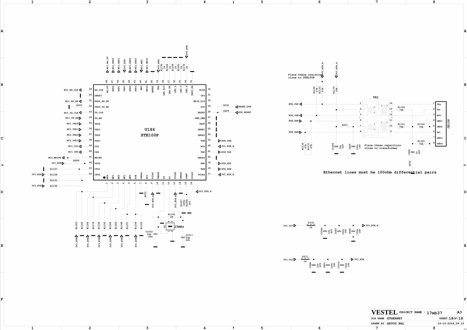
47R
R1132
10R
R1170
R1133
47R
TR1
16
15
1413
12
11
10
98
7
65
4
3
2
1
X1
2
41
3
ETHERNET
ERTUG BAL
18 18
17mb37
87654321
A
B
C
D
E
F
AX M
1 2 3 4 5 6 7 8
A
B
C
D
E
F
OF:
A3PROJECT NAME :VESTELSCH NAME :
DRAWN BY :
SHEET:
14-10-2009_09:10
JK108
8
7
6
5
4
3
2
1TX+
TX-
RX+
GND1
GND2
RX-
GND3
GND4
75RR1121 R1126
75R
S263
50V22p C1017
S262
16V
100n
C1014
75RR1125
1kV
1n
C996
75RR1120
MII_RXD1
MII_TX_EN
MII_CRS
MII_RXD2
MII_RX_ER
MII_RX_CLK
MII_RXD3
MII_RX_DV
MII_MDIO
3V3_ETH_A
6V3
10u
C1004
MII_MDC
MII_COL
MII_TXD3
MII_TXD2
3V3_ETH
MII_TXD1
MII_TXD0
MII_TX_CLK
3V3_ETH
R1183
R1192
R1191
3V3_ETH R1188
R1187
3V3_ETH
RESET_DVB
MII_MDINTR999
220k
R1207
5k1
R1208
ETH_RESET
S230
S229
1k
R1181
R1189
1k
MII_RXD0
ETH_RXP
ETH_RXN
ETH_TXP
ETH_TXN
R1134
47R
47R
R1131
1MR1145
C101622p 50V
ETH_TXP
ETH_TXN
3V3_ETH_A
ETH_RXP
ETH_RXN
3V3_ETH_A
S247
16V
100n
C890
3V3_ETH_A
50V
15n
C1005
S255
3V3_ETH_A
3V3_ETH_A
3V3_ETH_A
R1182
R1180
R1179
R1185
3V3_ETH
3V3_ETH
R1196
R1195
R1184
3V3_ETH
3V3_ETH
3V3_ETH
R1198
R1197
3V3_ETH
R1194
R1193
1k
F278
STE100PU186
16
15
14
13
12
11
10987654321
32
31
30
29
28
27
26
25
24
23
22
21
20
19
18
17
33
34
35
36
37
38
39
40
41
42
43
44
45
46
47
48
49
50
51
52
53
54
55
56
57
58
59
60
61
62
63
64 CFG0
CFG1
VDD2
MDINT
CRS
COL
TXD3
TXD2
TXD1
TXD0
TX_EN
TX_CLK
TXD4_TX_ER
RXD4_RX_ER
GNDE3
RX_CLK
RX_DV
RXD0
RXD1
VDD1
RXD2
RXD3
MDC
MDIO
GNDE2
VDD
LED_R10
LED_TR
LED_L
LED_C
LED_S
TEST_SE
VCCA4
RXN
RXP
GNDA4
TXP
NC2
TXN
GNDA5
GNDE1
TEST
PWR_DWN
RESET
RIP
MDIX_DIS
CF2
SCLK
MF4
MF3
MF2
MF1
MF0
FDE
GNDA1
NC1
VCCA1
GNDA2
X2
X1
VCCA2
GNDA3
IREF
VCCA3
R1178
1k
1k
R1186
3V3_VCC
16V
100n
C891
3V3_ETH
6V3
10u
C998
F271
1k
3V3_VCC
R1190
1k
16V
100n
C859
C866
100n
16V
3V3_ETH
3V3_ETH
3V3_ETH_A25MHz
close to STE100PPlace these resistors
close to transformerPlace these capacitors
Ethernet lines must be 100ohm differential pairs
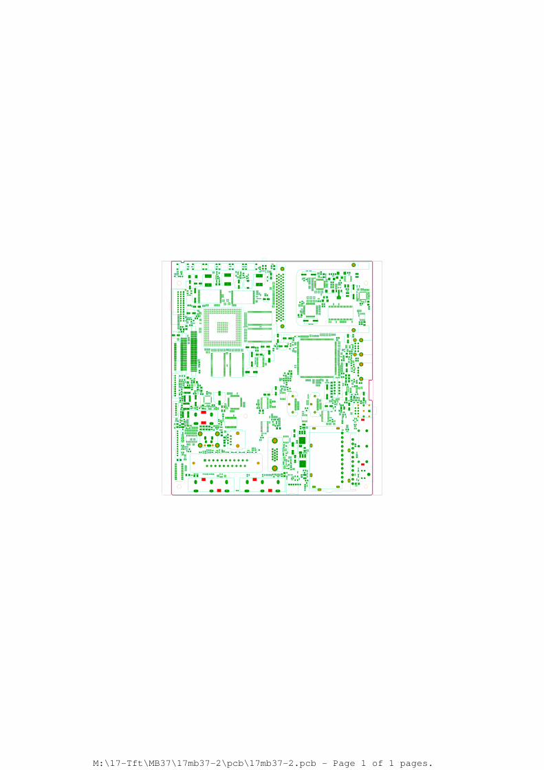
M:\17-Tft\MB37\17mb37-2\pcb\17mb37-2.pcb - Page 1 of 1 pages.
G
G
G
DB
C1029
C1020
C1024
R1342
CN130
C1055
R1276
R1102
C1075
C1137
C1034
R939
C893
C897
R890
R892
R891
C836
F248
R1217
JK106
C1030
R1210
R1212
C900
U177
C894
C895
R1221
U165
C1127R211
C624Q134
C625
C112
D114
D113
F236
F287
R1057
R1058
R562
D136
C368
D3
C123 U128
C502
C626
TU101
F254
U151
C892
X109
C896
C1077
C1128
R564
R565
C369
C361
C632
C633
R212C538
D126
C386
R545
Q135
R1300
C213
R964
R268
R271
F187
R228
C660
C659
L104
R125
R623
TU102
C1159
U174
R1337
F157
C202
R357
C194
S220
C178 F125
C155
R270
R229
R757
R288
C661
C499
R419
R686
F120
C149
C145
C510
C148
F186
C546
L101
Q144
S308
C1064
R264
R1312
R110
R473
C721
F238
C1162
F256
C446
D145
R111
C586
C136
C1023
C1161
R1309
R351
C435
R664
R18R12
R10
R1063
R1062
R1116 R1341
C221
F127
F128
U138
R140
R14
R13R15
R11
R17
R908C906
R1141
R1042
C305
C152
C420
R16
S105
C1027
R909
R1083
C908 R911
R910
C1019
S266
R1077
C1025
S267
R1172R1173
R427
C157
R1316
R293
R133
R632
R476
R1018
C206
R331
R394
U123
R163
R298
R1060
C224
C658
D174
R289
R389
R391
R390
R386
R385
R388
R387
R1282
C1069
U122
R408
D150
CN121
R1265
C182
R1165
R1129
C1076
C1045
D155
R724
S244
R629
U112
C972
R506
R970
C940
S120 R164
C174
F188
R167
U159
Q147
R507
C116
R1065
R1071
D147
U110
C383
R349
R242
U157
C1036
D178
R1093
C903
C1094 R241
R200
C1149
Q126
S194
C531
R1044
R199
R1049
C967
R472
R471
R1023
C968R36
R957
R34R35R33
C1151
C529
R234
S217
R907
C989
C1006
F208
R1052S249
R902
R906
R903
R921
R898
R899
R915
F239
F274
C445
R663
F260
F151
D167
R281
Q128
D111R120 R646
F209
SW3
R193
X106
C973
C103
R640
R1252
R448
R1289
R1298
U155
S262
R644D117
F215
R969
R440
C790
R318
R1131
R1331
R1101
R182
R999
R1192
C866
TR1
R643
SC101
C793
R1112 R432
R1273
C1079
R1249
C107
R638
R1332
C850
S241
S243
R217
C1053
R1294
C1084
R1295
Q184
D104
R888
R1159
R433
R28
R596
SW5
R1089
C14
C489
C1093
S302
R213
C475
F194 F198
R1085
C1142
C365
C754
R1082
S242
F242
F241
R1318
S298
R1319
C1131
R1233
S281
R639
FS6
C1133
L3
R793
L2
C1113
R1288
R1330
R1251
R1292 R1333
R1271
C842
C788
R1270
R22
R21R23
R705
S20
S291
S295
S283
R1317
F5
R1223
R792
R381
R531
S125
R1287Q148
R1235
S294
S293
U194
S277
C1049
R1268
C1139
C1059
R1250
C1060
C1061
S306 R682
R265
CN4
C1078
C1116
C3
F290
F288
S280
S289
S193
Q125R608
D182
S23
C753
R552
R422
CN106 C1114
CN3
R41
C5
R276
R421
R43
R1285
F289
F291
F292
R1254
C1035
R950
R1031
R1032
R1016
C541
JK110
C933
F191
JK102
R1222
R1220
S250
R1160
CN132
CN131
C899
S236
C934
C931
S233
S259
S257
C1126
C122
R237
R423
C503
R800
R1211
C819
R893
C925
C926
D125
D185
C473
C532
F159
R504
R889
C898
R1144
F249
S228
F250
C665
R544
F216
F211
C113
F212
C474
R624
S104
C111
C359
R563
D135
R801
C520
C1068
U167
F251
Q136
Q151
R569
R706
C537
R1290
R1291
C818
U166
C469
R238
F185
C540
C811
R1335
R1336
R1069
R1035
R1140C611
C129
R424
R384
C914
C913
L116
Q175
C1062
R1313
R1036
C555
R599
L114
R38
R680
D166
Q176
U195
R1324
R1338
C1067
R1315
R1314
R1334R295
R296
R269
R420
C554
R598
R519
R520
S106
C142
C498
Z102
C547
R735
R483
R252
C135
C545
L111
F237
R1059
C849
R858
R857
R474
R928
C945
R1209
C1063
R253
Z101
Q140
R210
D121
R505
R595
R1266
D165
C1160
R1310
C363
R231
C467
R209
R594
Q116
C1157
C1065
C1066
C364
C448
C128
R254
C587
R127
R1153
C1031
C723
R1311
R748
U115
C1032C695
C1026
C1021
C750
C283
D164
C447
X104
R126
F255
C799
U152
C916
R239
R314
R1323
C425
C416
C433
R649
R9
R8
C137
C1022
S235
S234
R171
R313
R1098
C1041
R141
R859
CN122
R1322
C423
C422
C419
R652
R653
C910
R1117
C188
R119
C173
R499
R134
R145
R144
R1167
R1043
U109
C304
C151
C150
C1028
X108
C907
R1084
R1168
C909
C941
R1078
C937
R1174
R426
X101
Q171
R412
C159
R494
C452
C134
R503
Q115
R501
Q102
TH101
R502
F234
R803
R524
R286
R279
R287
R493
D193
U193
R378
R411
C360
R460
R622
F231
R332
R482
Q170
C225
C904
R1061
C657
C929
R294
R290
F279
C1158
C598
F286
C183
F116
C176
R278
C311
R356
C154
C308
R1248
C470
C600
R1072
D152
U130
R1164
C138
R1119
Q168
R1067
C409
F145
C306
C752
Q123
R396
R511
C854
Q167
Q165
CN114
R1166
L119
R393
R392
D146
C439
C438
C437
S238
CN116
C1129
Q172
S265
L117
C736
R491
R492
R584
D102
R712
R711
D101
S245
R1033
D172
C366
C1007
CN118
C994
C153
C530
R355
F118
C821
R1224
C995
C917
R257
R233
R745
R354
S123
R352
R353
C602
R464
R324
C738
F247
C453
R1345
C1163
C1037
R323
F261
F259
S121
R232
Q127
R752
Q117
C1095
C958
C974
C443
S196
F280
R1053R333
C957
R683
R662
C444
C986
R661
C987
S18
S195
C180
C229
S192
R400
C739
R965
U127
CN142
C845
S258
R966
U129
R284
C479
C115
L118
C846
L125
R904
R905
C992
R282
R280
C844
R897
U156
R315
U154
U180
C147
JK104
R1143
C923
C924
R128
D112
C1054
L110
R1274
C782
C106
C480
S21
R451
R434
R445
R442
R439
R435
R1181
R1305
Q177
U172
R452
R441
R186
R443
R438
R1189
R1190
R1186
R1178
D115
C1092
R1299
C464
R449
SW1
Q182
JK108
D179
R955
R968
R1007
R1114
U186
R1132
R1133
R1170
R641
L124
R1151
R447
R1134
R1039
R1103
R1187
R1188
R1191
D116
R1111
R453
R1145
C1005
C890
R1121
R1125
R1120
C104
C105
C442
SW4
U160
R189
C1016
X1
C1017
S247
C996
R1126
S255
R637
R1253
FS3
R946
R967
C12
F207
D106
C108
C441
Q181
C1085
Q183
U153
C488
Q180
R1296
C735
C977
R436
R44
R1297
D184 F204
R216
D186
D140
L122
U169
R1130
C706
C1155
U1
R30
R255
C140
JK109
R1091
R1090
R29
R26
S13
F205
D183
S19
F196
C477
JK101
R1099
R885
R1162
R1163
C484
F195
R886
R880
R1320
C13 S16
JK111
FS5
R219
C478
C7
R937
R1154
S2
R3
R6
R5
F2
C1130
C1042
C1056
Q2
S282
SW6
R1100
R1055
R1095
C774
R1124
R942
R1155
F1
C1132
U192
S17
FS4
R1284
F197
CN1
R1328
X107
D137
CN2
D2C1057
U191
C1134
C1115
R1230
R1228
C1141
C8
R568
C1043
F3
S279
S12
R20
C1120
C1118
R1232
S276
R1229
R1231
S292
S278
R1325
C440
C826
S22
S290
S1S3
D1
C668
C1119
R1234
R1237
R1239
Q178
D181
D180
C1052
F253
R37 R32
S4
L4
L1
F4
Q149
R528
C1143
R1236
C1144
R1238
R1327
R1326
R1240
R277
R39
C1117
S117
Q158
D194
C1121
R1286
SW2
C1051
C1091
CN138
D148
D149
R526
S119
R527
S118
F6
R382
C1044
C1135
R1267
C1050
C1136
R1269C1140
S299
R1329C1138
F293
CN137
CN144
S6S5
CN140
CN139
Q131
Q130
C1090
CN141
R267
C20
D130
F228
F230
F229
C608
F225
C6CN119 R42
R40
C19
C18
C4
F7
FS1
CN143
S307
R1275
CN115
R1272
D187
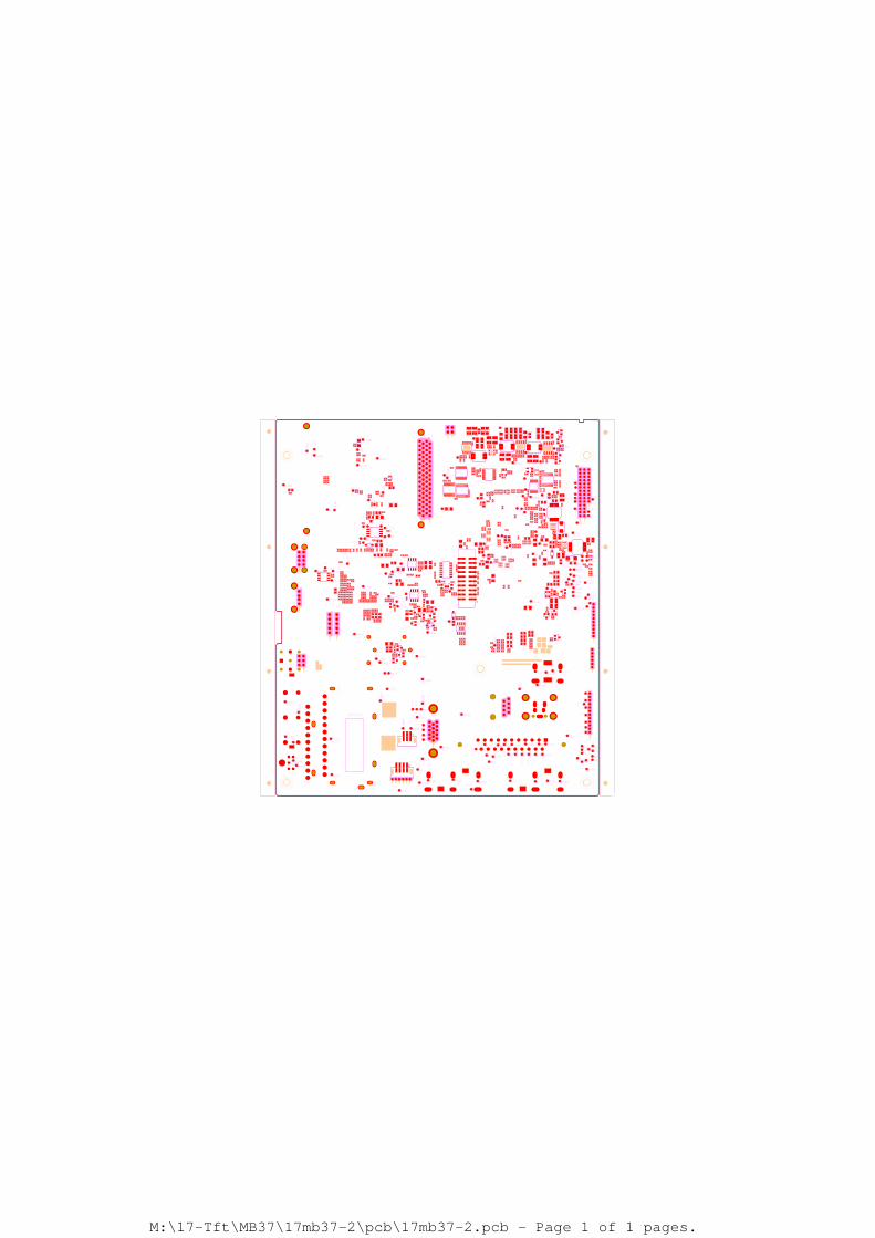
M:\17-Tft\MB37\17mb37-2\pcb\17mb37-2.pcb - Page 1 of 1 pages.
G
BARKOD
CN122
1
1
1
1
1
1
1
TOP
TOP
1
1
CN116
1
1
1
1
1
1
1
1
1
1
1
1
DB
TP295
TP291
TP283
TP158
TP236
TP110
TP112
TP276
TP278
TP116TP228
TP106
TP119
TP225
TP410
CN145
TP159
TP239
TP133
TP111
TP304
TP305
TP274
TP303
TP289
TP301
U163
TP238
TP299
TP144
D191
TP259
TP227
TP302
TP281
TP387
U175
TP280
TP243
TP380
TP260
TP28
TP256
TP391
TP385
TP201
TP33
U178
U184
TP406
TP394
TP347
TP292
TP397
TP401
TP395
TP13
TP26
TP30
TP29
TP389
TP407
TP396
TP12
TP10
TP19
TP8
TP18
TP266
TP298
TP282
TP297
TP290
TP375
TP273
TP109
U103
TP229
TP118
TP277
TP237
TP117
D169
TP279
TP160
TP296
TP246
Q103
TP275
TP242
TP409
TP383
U182
TP113
TP115
Q179
TP411
TP143
TP101
CN135
TP240
TP365
U117
U118
TP353
TP384
TP306
TP197
U181
Q166
TP288
TP241
Q120
D127
D124
CN136
TP350
TP378
TP300
U173
TP142
U162
TP356
U144
U164
TP231
TP360
TP253
U171
U190
TP235
TP377
TP388
TP262
TP261
TP257
Q104
TP357
TP362
U187D188
TP258
TP149
U158
TP247
TP252
C2
TP348
Q157
Q139
TP284
Q162
TP198
TP24
TP390
TP17
TP25
TP23
TP400
TP392
TP202
TP6
TP4
TP408
TP402
TP3
TP1
TP16
TP376
TP150
TP249
TP151
TP108
TP230
U132
TP161
TP412
TP114
Q154
Q119
TP132
Q150
TP366
Q133
Q146
Q132
TP103
TP104
TP102
TP105
TP134
Q121
TP234
TP307
U161
TP233
Q169
D170
U189
TP361
TP255
TP287
TP346
TP244
TP15
TP251
TP355
D190
TP250
TP354
TP351
TP254
TP352
TP294
TP359
TP358
U170
TP363
TP226
TP232
TP336
TP293
TP334
D177
D176
TP335
U168
U183
Q137
TP248
D158
TP21
TP403
Q163
TP381
D159
L120
Q1
TP386
TP22
TP11
TP405
TP404
TP14
TP31
TP399
TP398
TP7
L121
TP27
TP382
TP2
TP393
TP20
TP5
TP9
TP288
TP258
TP400
TP406
TP394
TP290
TP266
TP283
TP295
TP236
TP150 TP110
TP158
TP273
TP112
TP276
TP151
TP278
TP229
TP160TP116
TP106
TP117
TP132
TP409
TP383
TP230
TP239
TP133
TP410
TP301
TP134
TP353
TP101TP103
TP366
TP350
TP378
TP241
TP238
TP233
TP142
TP227
TP356
TP361
TP302
TP255
TP388
TP280
TP262
TP257
TP254
C1110
TP387
TP235
TP261
TP250
TP359TP360
TP354 TP363TP358
TP248
TP260
TP252
TP292
TP381
TP380
TP256
C1153
C1145
Q137
TP347TP385
TP335TP336
TP362
TP33
TP201
TP26TP198
TP397
TP395
TP396
TP202
TP24
TP31
TP23
L121
TP393
TP398
TP401
TP389
TP407
TP404
TP390
TP392
TP386
TP13
TP20
TP11
S10
TP298
S7
TP297
TP291TP282
TP375
TP376
TP109
R261
U103
R262
TP108
C201
R227
C495C645
C642
C636
R1277
R395
R415
C551
C494C644
C497
C493
C655
C656
R514
TP279
TP228
R650
C427
R655
TP296
C912
TP277
C700
C748
R463
R469
C1112
C434R142
R147
F264
C215
F124
C430
R659
C214C223
TP237TP246
F150
C605
C501
C612R773
R829
TP113
R467C378
Q154
R1037
C1033
R365
R1283R1280
C156
R1279
TP242
TP225
R1264
R620
TP412TP411
TP143
Q146
TP240
Q133
TP365
U118TP159
R738
R737
R736
R729
R402
C121 C375
C631
R750
S128
Q132
TP304
TP104
TP306
C374
C120
C372
R751
R521
R522
C371
D127
R541
R1241
TP384
TP102
TP303
TP305
TP197
TP274
TP289
C834
S126
C742F258
R1068
S127
R1321
U163
R998
S275
TP300
R1293
C829
U162
C676
S231
D170
F257
U173
C1104
C1047
R917
R1025
R873
R876
R874
TP299
D191
R925
C832
C993
R877
R872
C798
TP259
C704
C675
S229
TP287
C535
R1024
C730
TP244
C891
C1014
TP346
TP15
TP294
C1109
R1045
TP253
F265TP251
R1195
R1207S263
TP144
S210
C1099
C831
R1109 R1118
C729
R1106
R1115
R1107
C998
F271
R1182F278R1179
R1208R1193
R1185 C1004R1197
TP355TP351
C1074
C1083
R1008
R1019
R884
C780
F277
C1111
U190
C853
R1110
R926
R927
C794
TP281
C777
R1343
C247
C677
TP352
U178
R940 C772
R954
R1139
TP247
C795
C693
TP232
TP226
C1102
C1103
D188
C840
U175
F267
R879
R1015
C705
R938
R951
R949
C771
R1064
C808
TP243C1152
TP334
TP348
TP357
D159
D158
C1046
F276 C759
R1149
Q1
TP284
R914
C816
R929F262
C1
TP149
R19
TP21
TP391
TP403
TP405
R7
TP6
TP1
TP4
TP17TP2
TP30
TP29
C814
S9
TP399R2
R1243
S285
TP408
TP402
TP27
TP382
TP12
TP10
TP14
TP19
TP8TP16
TP18
C935C384
C181
C756
C936
C757
C356
TP249
R840
F184
C552R223
R515
C131
C130
C132
R1278
R1261
R283
R414
R413
C548R222
C549
R627
R224
R225
R226 R417
C550
R416
R516
R518
C643 R600
C496
R513
C492
R418
R605
R517
C597
C620
C758
C199
C200
C553
R603
R601
R607
R606
R654
C927
C911
C946
C749
C699
R312
R311
R761
C197
C198
R146
C424
C160
TP118
C216
R407
R117
C905
R651
R666
C490
C428
C426
R656
R657
Q103C227
D169
R536
R535
C196
R139
C417
C143
R687
C432R143
R403
R149
R148
TP275
C228
C725
R665
C429
C431
C491
R660
R404
R658
C207
C217
C930
U132
C184
C193
C195
R667
R138
C418
R137
C421
R830
R831
TP161
TP119
TP115
TP111
C220
R291
F119
S239
S240
C830
R742
R292
C410
C158
TP114
Q179
R161
F147
R1263
R221
U182
C743
R1038
S256
C928
R162
C307
C175
C177
C144
R630
R1281 R258
C666 R674
R777
R753
C649
C367
C408
F146
Q119
CN145
R722
C385
R739
C650
C662
C663
CN135
R678
U117
R677
F217
C119
R676
R675
C118
R153R689
R236
S296
R542
Q150
F219
TP105
R692
R685
C646
R684
R691
R690
R155
C630
R546
R1048
Q120
R1020
Q121
R1054
D124
Q166
R185
R274
R870
R375
C251
TP234
TP307
R1050
U161
U181
Q169
C289
C737
R901
R900
R871
S270
C810
R1227
C789
C991
R918
S232
R1156
C1125
R1246
C1081
C249
R1001
CN136
R1225
R1226
S271
C990
C988
U189
R1304
C248
R1157
R1158
C1105
R1003
C1072
R924
R922
R919
R920
S300
C1089
C575
F270
C1156
R446
C579
R956
R923
R916
C797
R450
F273
F252
R875
F8
S301
C576
U164
R963
R188
C734
R183
C765
C273
S230
S134
R818
R249
U144
R958
R936
R934
C751
R437
R1150
R444
F240
S269
R1004
C578
R1022
R1196TP231
C859
R702
R1113
C702
C767
C250
C791
C709
R1104
R1183
R1180
R1184
R1194
R1198
C1108
R1021
R1009
C716
F266
C266
R1002
C1100
D190
U171
R959
C728
R1105
R1242
C1124
R1262
C841
R883
R887
R881
R1308
R1303
R1108
C715
R190
TP377
S305
R1339
R1340
C1058
R944
R945
R878
C15
R1344
C10
C11
C16
C1097
C733
R1046
R1056
R1079
C9
R27
C1088
U170
C852
R1051
R1005
R1076
C732
C731
C976
R1034
R1014
R1066
C713
C720
C803
C804
S15
R25S14
R31
R24R123
TP293
C1098
C851
R1012
R953
U158
C828
R1013
C792
R1047
R882
R952
R1074
C726
R1257
C1122
R1245
C1080
F268
C1154
R1146
Q104
R571
S303
U187
R1306
R1301
U168
D177
C761
C920
R1142
C719
C717
R708
R1255
C1071
R1260
R943
C981
C801
C978
L120
R1152
R1147
D176
R1148
R205
R566
C1086
R1256
R1259
R948
R894
C843
R896
C921
R895
F269
F246
U183
C876
R931
R1176
F172
R1F285
F170
F171
C618R
700
C17
C2
R575
Q139
C309
S11
Q162Q163
R913
R1000
R941
R1169
C812
C764
C918
F243
R794
R912
C922
R1092
D161
F244
U184
R930
C875
R1075
C815
Q157
S216
R4
D162
TP22
TP28
TP25
TP3
C779
S8
S287R795
TP7
TP5
S284
S286
S288
R1244
TP9