Embed Size (px)
Citation preview
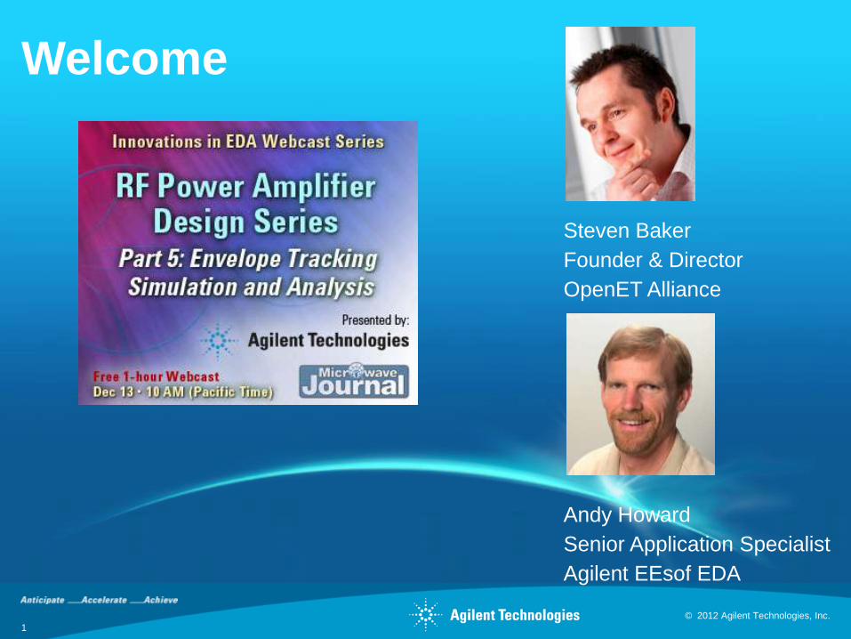
Welcome
1
© 2012 Agilent Technologies, Inc.
Andy Howard
Senior Application Specialist
Agilent EEsof EDA
Steven Baker
Founder & Director
OpenET Alliance
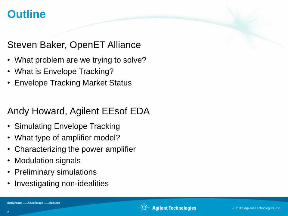
Outline
Steven Baker, OpenET Alliance
• What problem are we trying to solve?
• What is Envelope Tracking?
• Envelope Tracking Market Status
Andy Howard, Agilent EEsof EDA
• Simulating Envelope Tracking
• What type of amplifier model?
• Characterizing the power amplifier
• Modulation signals
• Preliminary simulations
• Investigating non-idealities
2
© 2012 Agilent Technologies, Inc.
Envelope Tracking—An Introduction
Steven Baker, OpenET Alliance
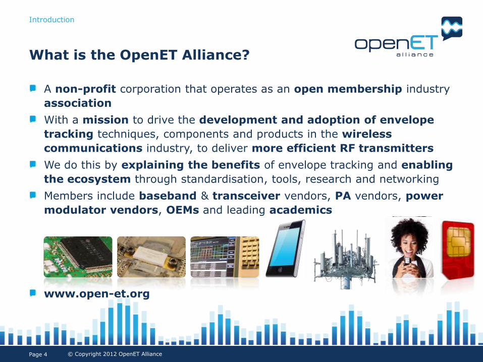
What is the OpenET Alliance?
A non-profit corporation that operates as an open membership industry
association
With a mission to drive the development and adoption of envelope
tracking techniques, components and products in the wireless
communications industry, to deliver more efficient RF transmitters
We do this by explaining the benefits of envelope tracking and enabling
the ecosystem through standardisation, tools, research and networking
Members include baseband & transceiver vendors, PA vendors, power
modulator vendors, OEMs and leading academics
www.open-et.org
Page 4
Introduction
© Copyright 2012 OpenET Alliance
What’s the problem?
What’s envelope tracking and how does it help?
Market status
© Copyright 2012 OpenET Alliance Page 5
Outline
Introduction
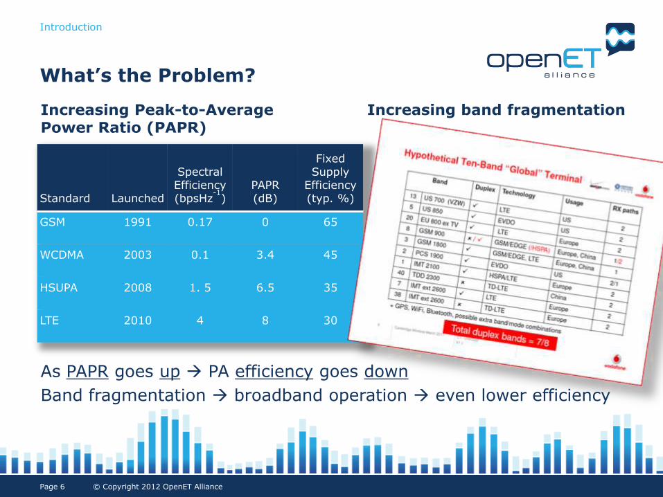
Increasing Peak-to-Average Power Ratio (PAPR)
© Copyright 2012 OpenET Alliance Page 6
Standard Launched
Spectral Efficiency (bpsHz
-1)
PAPR (dB)
Fixed Supply
Efficiency (typ. %)
GSM 1991 0.17 0 65
WCDMA 2003 0.1 3.4 45
HSUPA 2008 1. 5 6.5 35
LTE 2010 4 8 30
What’s the Problem?
Introduction
Increasing band fragmentation
As PAPR goes up PA efficiency goes down
Band fragmentation broadband operation even lower efficiency
© Copyright 2012 OpenET Alliance Page 7
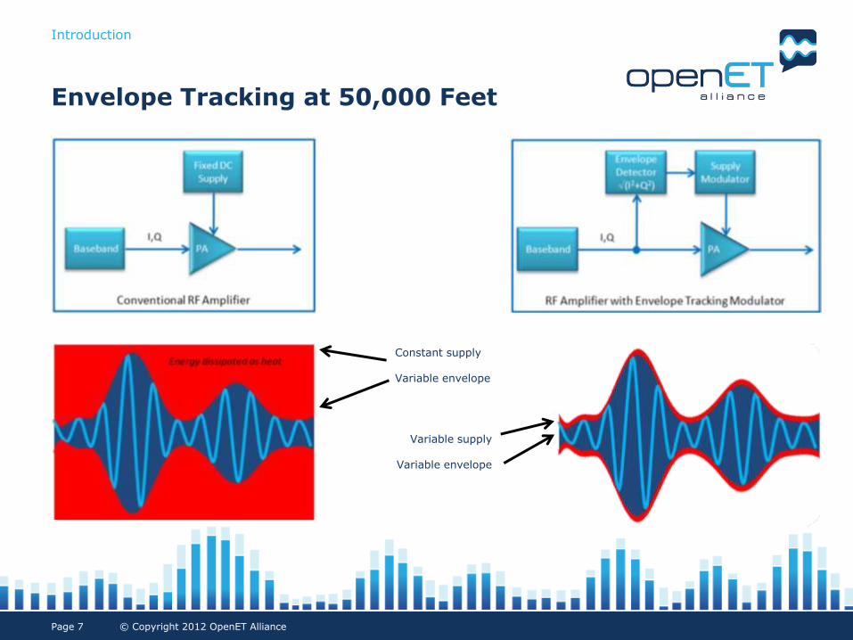
Envelope Tracking at 50,000 Feet
Introduction
Constant supply Variable envelope
Variable supply
Variable envelope
© Copyright 2012 OpenET Alliance Page 8
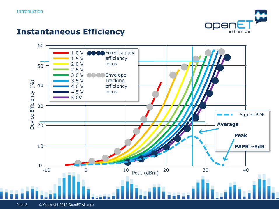
Instantaneous Efficiency
Introduction
60
50
40
30
20
10
0
Devic
e E
ffic
iency (
%)
Pout (dBm) 40 30 20 10 0 -10
1.0 V 1.5 V 2.0 V 2.5 V 3.0 V 3.5 V 4.0 V 4.5 V 5.0V
Fixed supply efficiency locus Envelope Tracking efficiency locus
Signal PDF
Average
Peak
PAPR ~8dB
© Copyright 2012 OpenET Alliance Page 9
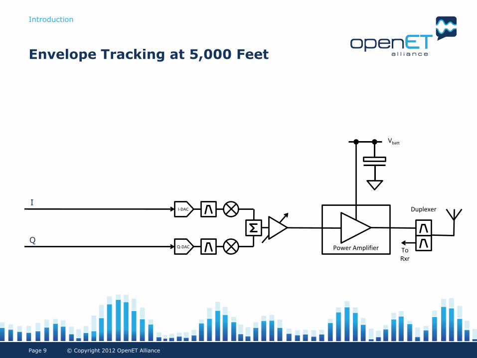
Power Amplifier Q-DAC
I-DAC
To Rxr
Duplexer I
Q
Vbatt
Envelope Tracking at 5,000 Feet
Introduction
© Copyright 2012 OpenET Alliance Page 10
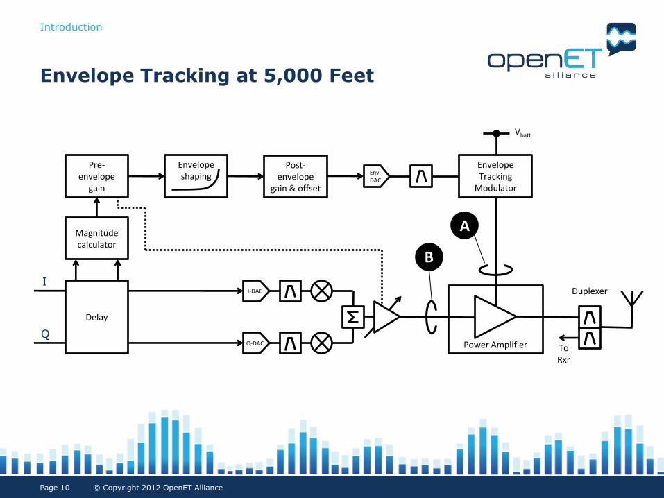
Power Amplifier Q-DAC
I-DAC
To Rxr
Duplexer I
Q
Env- DAC
Magnitude calculator
Pre-envelope
gain
Envelope shaping
Envelope Tracking
Modulator
Vbatt
Post-envelope
gain & offset
Delay
B
A
Envelope Tracking at 5,000 Feet
Introduction
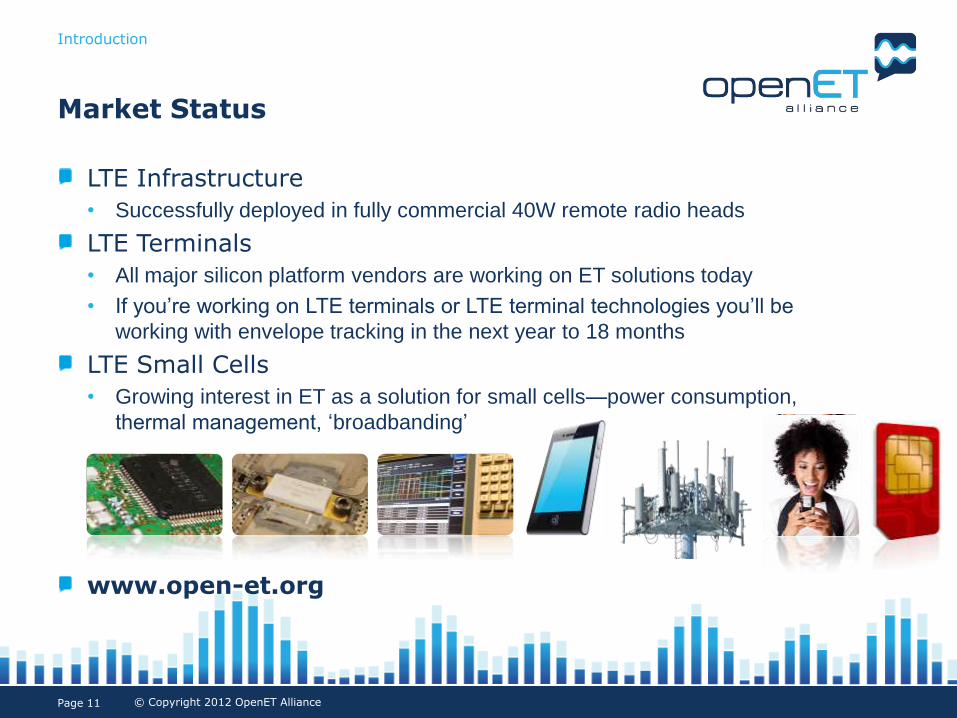
Market Status
LTE Infrastructure
• Successfully deployed in fully commercial 40W remote radio heads
LTE Terminals
• All major silicon platform vendors are working on ET solutions today
• If you’re working on LTE terminals or LTE terminal technologies you’ll be
working with envelope tracking in the next year to 18 months
LTE Small Cells
• Growing interest in ET as a solution for small cells—power consumption,
thermal management, ‘broadbanding’
www.open-et.org
Page 11
Introduction
© Copyright 2012 OpenET Alliance
Outline
Steven Baker, OpenET Alliance
• What problem are we trying to solve?
• What is Envelope Tracking?
• Envelope Tracking Market Status
Andy Howard, Agilent EEsof EDA
• Simulating Envelope Tracking
• What type of amplifier model?
• Characterizing the power amplifier
• Modulation signals
• Preliminary simulations
• Investigating non-idealities
12
© 2012 Agilent Technologies, Inc.
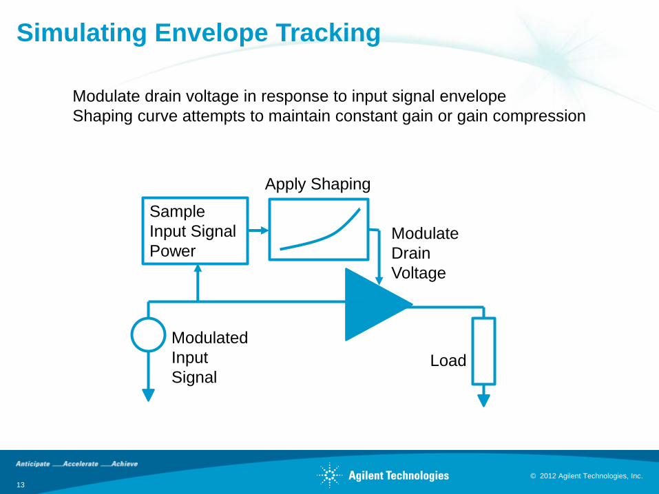
Simulating Envelope Tracking
13
Sample
Input Signal
Power
Apply Shaping
Load
Modulated
Input
Signal
Modulate
Drain
Voltage
Modulate drain voltage in response to input signal envelope
Shaping curve attempts to maintain constant gain or gain compression
© 2012 Agilent Technologies, Inc.
Outline
Simulating Envelope Tracking
What type of amplifier model?
Characterizing the power amplifier
Modulation signals
Preliminary simulations
Investigating non-idealities
14
© 2012 Agilent Technologies, Inc.
What type of amplifier model?
15
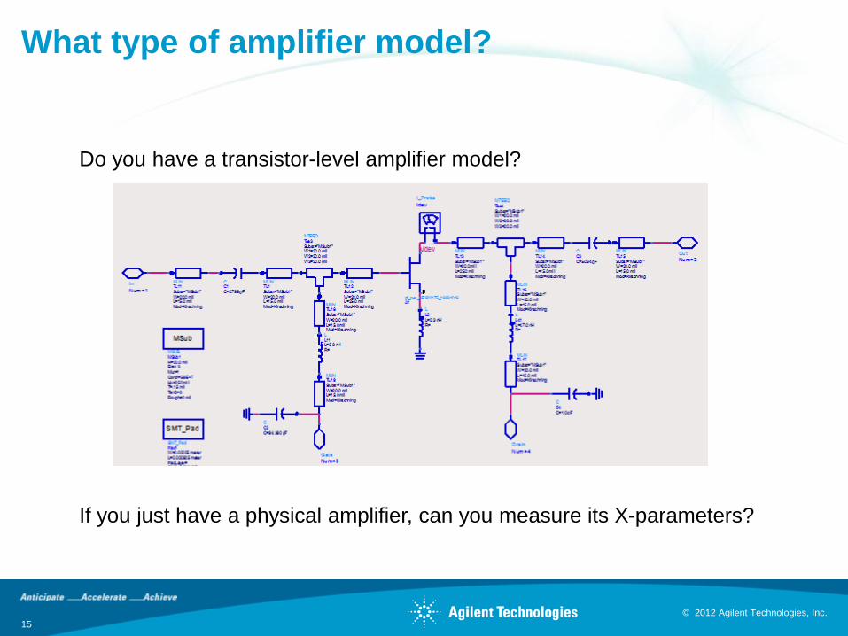
Do you have a transistor-level amplifier model?
If you just have a physical amplifier, can you measure its X-parameters?
© 2012 Agilent Technologies, Inc.

Outline
Simulating Envelope Tracking
What type of amplifier model?
Characterizing the power amplifier
Modulation signals
Preliminary simulations
Investigating non-idealities
16
© 2012 Agilent Technologies, Inc.
Characterizing the power amplifier
17
Checking for memory effects and bandwidth
Obtaining data for constant-gain shaping
Obtaining data for constant-gain-compression shaping
© 2012 Agilent Technologies, Inc.
Testing for memory effects
18
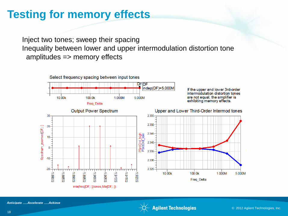
Inject two tones; sweep their spacing
Inequality between lower and upper intermodulation distortion tone
amplitudes => memory effects
© 2012 Agilent Technologies, Inc.
Testing for memory effects (a different amplifier)
19
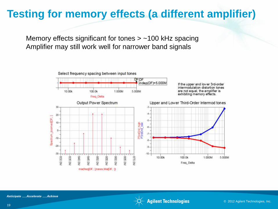
Memory effects significant for tones > ~100 kHz spacing
Amplifier may still work well for narrower band signals
© 2012 Agilent Technologies, Inc.
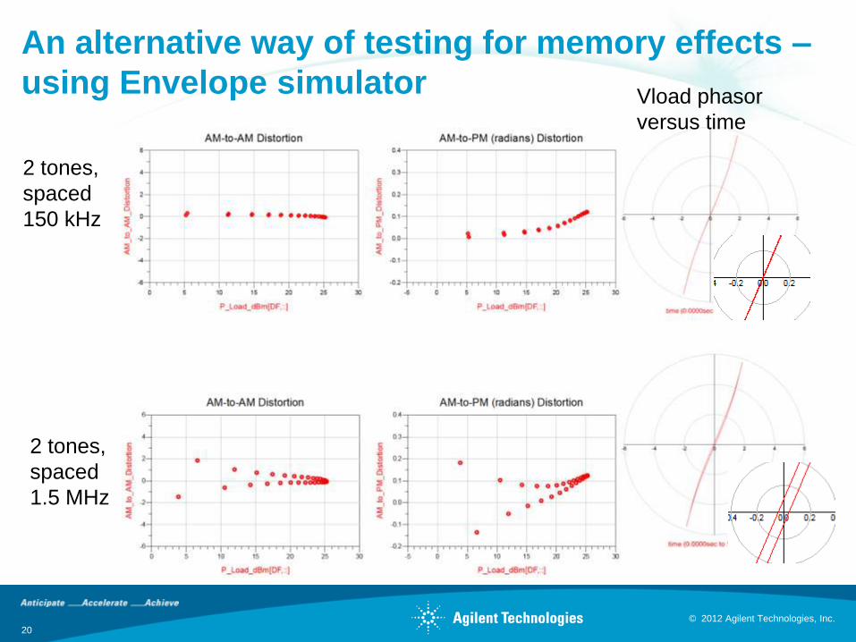
An alternative way of testing for memory effects –
using Envelope simulator
20
2 tones,
spaced
1.5 MHz
2 tones,
spaced
150 kHz
Vload phasor
versus time
© 2012 Agilent Technologies, Inc.
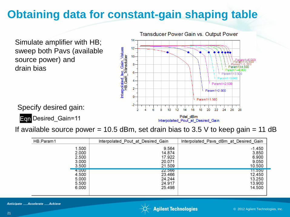
Obtaining data for constant-gain shaping table
21
Simulate amplifier with HB;
sweep both Pavs (available
source power) and
drain bias
Specify desired gain:
If available source power = 10.5 dBm, set drain bias to 3.5 V to keep gain = 11 dB
© 2012 Agilent Technologies, Inc.
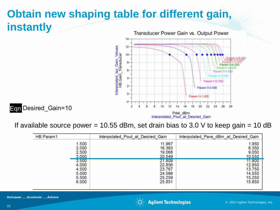
Obtain new shaping table for different gain,
instantly
22
If available source power = 10.55 dBm, set drain bias to 3.0 V to keep gain = 10 dB
© 2012 Agilent Technologies, Inc.
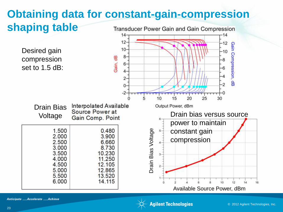
Obtaining data for constant-gain-compression
shaping table
23
Desired gain
compression
set to 1.5 dB:
Drain bias versus source
power to maintain
constant gain
compression
Available Source Power, dBm
Dra
in B
ias V
olta
ge
Drain Bias
Voltage
© 2012 Agilent Technologies, Inc.
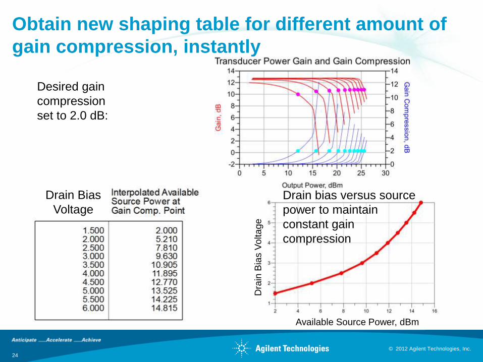
Obtain new shaping table for different amount of
gain compression, instantly
24
Desired gain
compression
set to 2.0 dB:
Drain bias versus source
power to maintain
constant gain
compression
Available Source Power, dBm
Dra
in B
ias V
olta
ge
Drain Bias
Voltage
© 2012 Agilent Technologies, Inc.
Outline
Simulating Envelope Tracking
What type of amplifier model?
Characterizing the power amplifier
Modulation signals
Preliminary simulations
Investigating non-idealities
25
© 2012 Agilent Technologies, Inc.
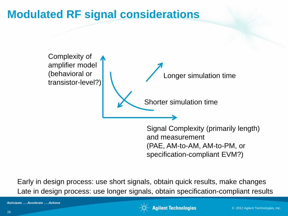
Modulated RF signal considerations
26
Complexity of
amplifier model
(behavioral or
transistor-level?)
Signal Complexity (primarily length)
and measurement
(PAE, AM-to-AM, AM-to-PM, or
specification-compliant EVM?)
Shorter simulation time
Longer simulation time
Late in design process: use longer signals, obtain specification-compliant results
Early in design process: use short signals, obtain quick results, make changes
© 2012 Agilent Technologies, Inc.
Obtaining modulated RF signals
27
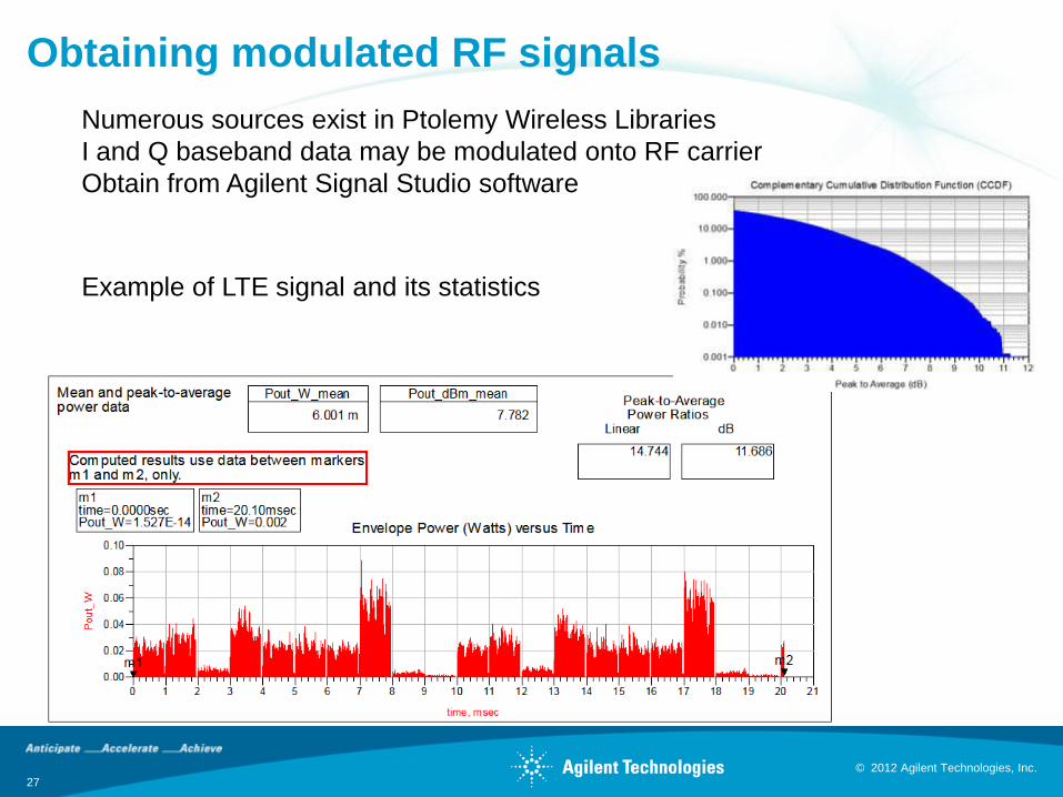
Numerous sources exist in Ptolemy Wireless Libraries
I and Q baseband data may be modulated onto RF carrier
Obtain from Agilent Signal Studio software
Example of LTE signal and its statistics
© 2012 Agilent Technologies, Inc.
Outline
Simulating Envelope Tracking
What type of amplifier model?
Characterizing the power amplifier
Modulation signals
Preliminary simulations
Investigating non-idealities
28
© 2012 Agilent Technologies, Inc.
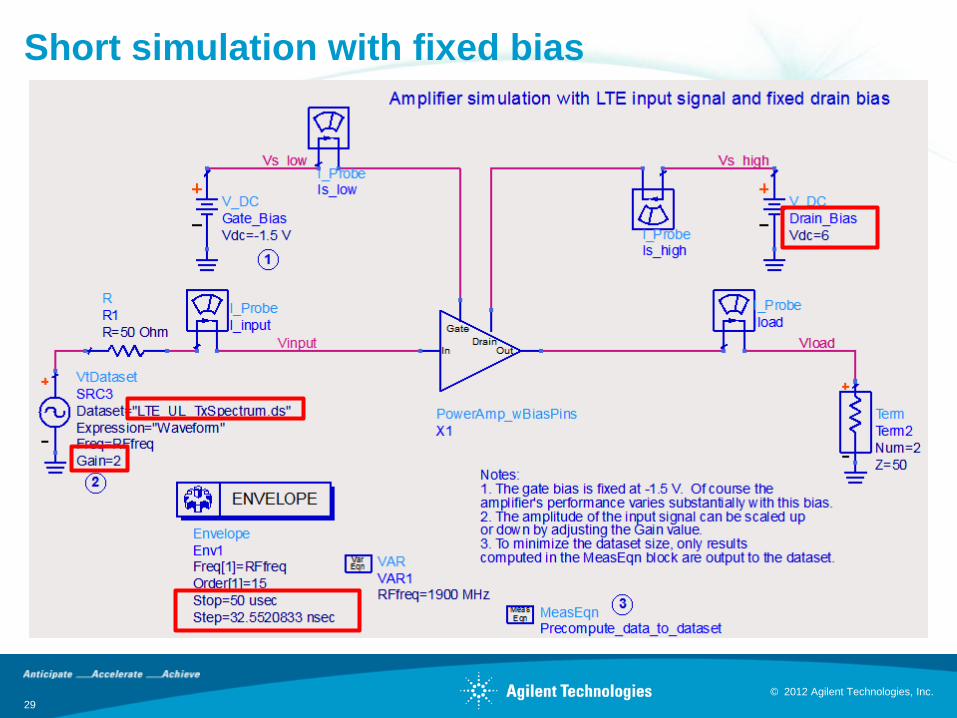
Short simulation with fixed bias
29
© 2012 Agilent Technologies, Inc.
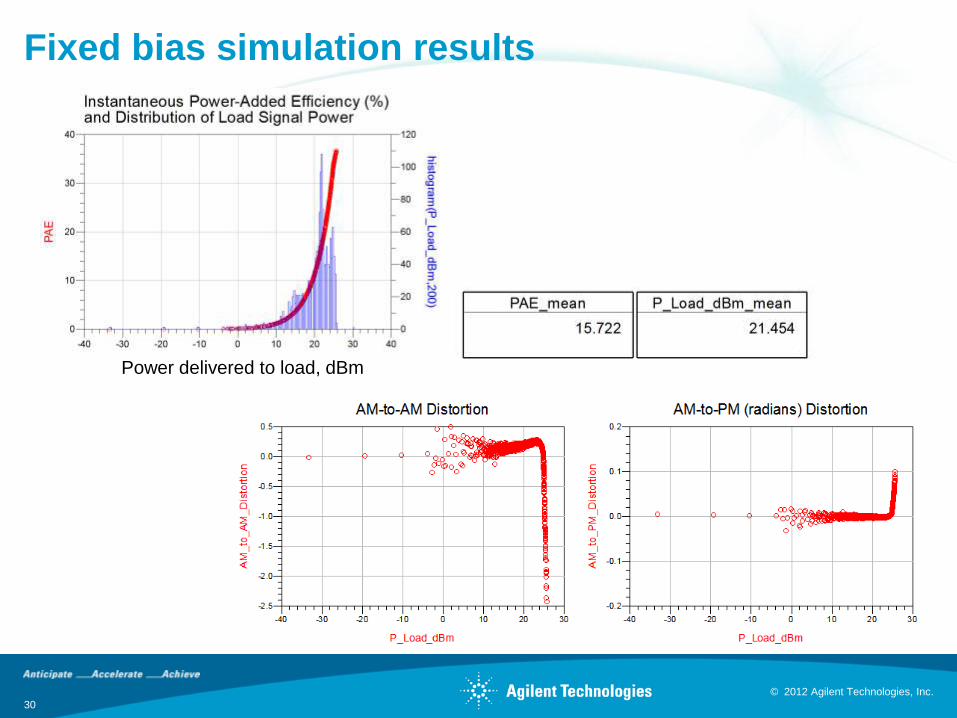
Fixed bias simulation results
30
Power delivered to load, dBm
© 2012 Agilent Technologies, Inc.
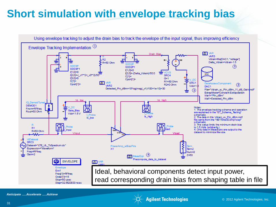
Short simulation with envelope tracking bias
31
Ideal, behavioral components detect input power,
read corresponding drain bias from shaping table in file
© 2012 Agilent Technologies, Inc.
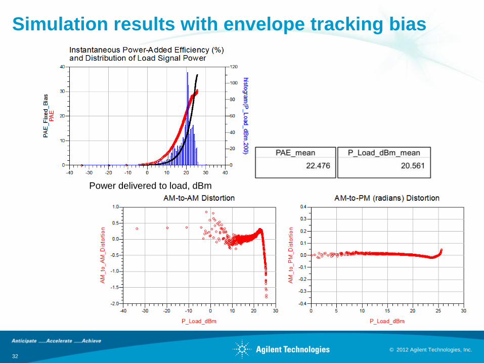
Simulation results with envelope tracking bias
32
Power delivered to load, dBm
© 2012 Agilent Technologies, Inc.
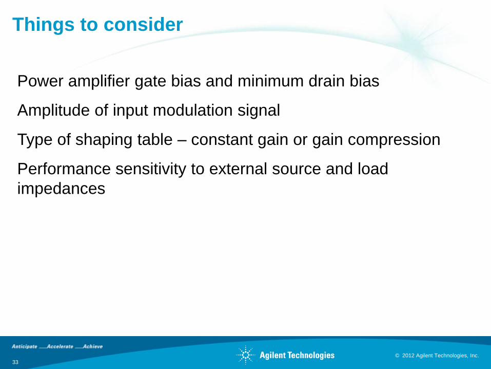
Things to consider
33
Power amplifier gate bias and minimum drain bias
Amplitude of input modulation signal
Type of shaping table – constant gain or gain compression
Performance sensitivity to external source and load
impedances
© 2012 Agilent Technologies, Inc.
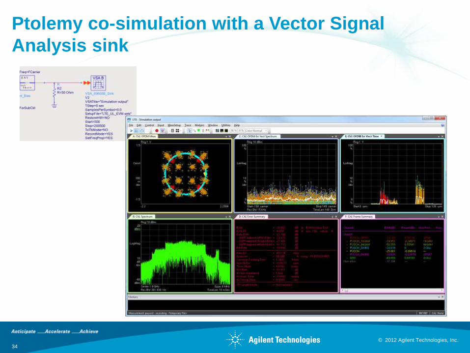
Ptolemy co-simulation with a Vector Signal
Analysis sink
34
© 2012 Agilent Technologies, Inc.
Outline
Simulating Envelope Tracking
What type of amplifier model?
Characterizing the power amplifier
Modulation signals
Preliminary simulations
Investigating non-idealities
35
© 2012 Agilent Technologies, Inc.
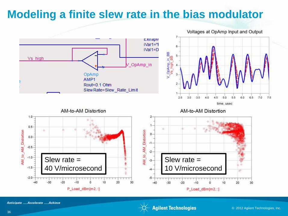
Modeling a finite slew rate in the bias modulator
36
Slew rate =
40 V/microsecond
Slew rate =
10 V/microsecond
© 2012 Agilent Technologies, Inc.
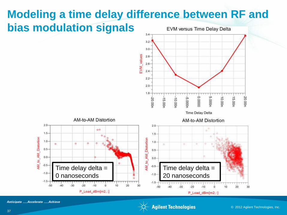
Modeling a time delay difference between RF and
bias modulation signals
37
Time delay delta =
0 nanoseconds
Time delay delta =
20 nanoseconds
© 2012 Agilent Technologies, Inc.
Summary
38
Agilent ADS – well suited for:
• Modeling power amplifiers
• Investigating power amplifier performance
• Generating and simulating modulated signals
• Investigating envelope tracking schemes
• Modeling various non-idealities
© 2012 Agilent Technologies, Inc.
For more information
39
Download these examples from the Agilent EEsof Knowledge Center: http://edocs.soco.agilent.com/display/eesofkcads/Applying+Envelope+Tracking+
to+Improve+Efficiency
Application note on envelope tracking simulation:
http://cp.literature.agilent.com/litweb/pdf/5991-1463EN.pdf
On envelope tracking:
http://www.open-et.org/
Or contact me directly: [email protected]
© 2012 Agilent Technologies, Inc.
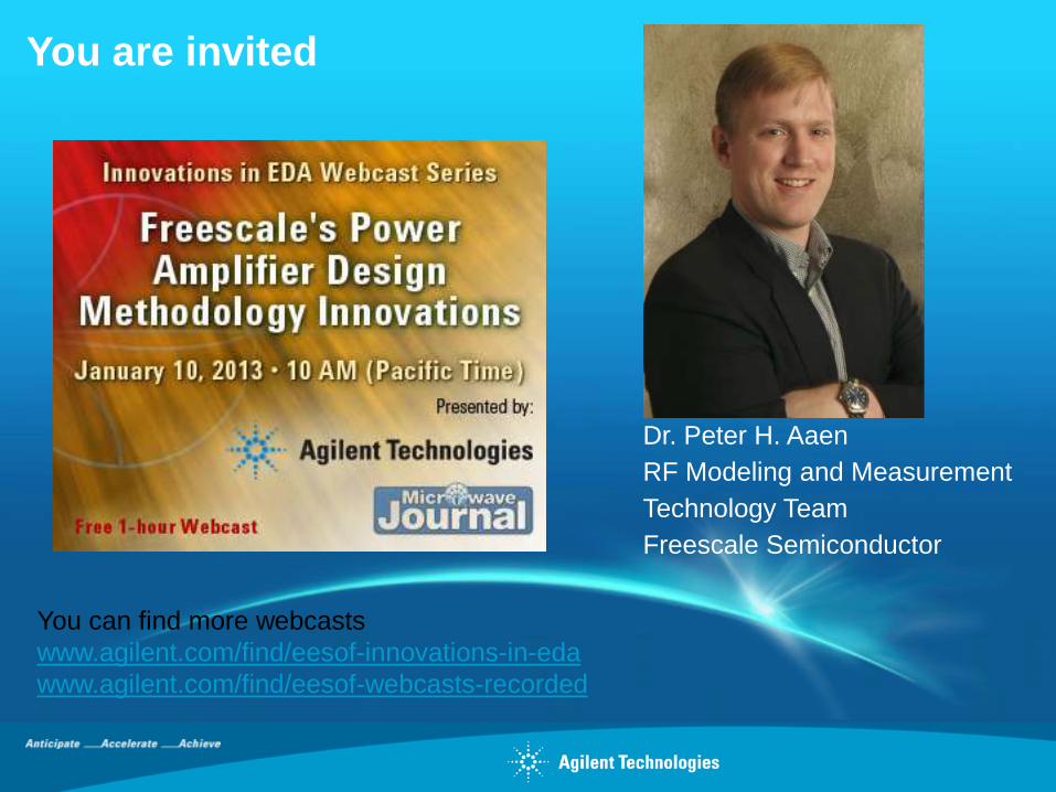
You are invited
Dr. Peter H. Aaen
RF Modeling and Measurement
Technology Team
Freescale Semiconductor
You can find more webcasts
www.agilent.com/find/eesof-innovations-in-eda
www.agilent.com/find/eesof-webcasts-recorded