Embed Size (px)
Citation preview
Stack up your chips: Betting on 3D integration toaugment Moores Law scaling
(Invited Paper)
Saurabh Sinha, Xiaoqing Xu, Mudit Bhargava, Shidhartha Das, Brian Cline and Greg YericArm Research, 5707 Southwest Parkway, Austin, Texas 78735
Email: [email protected]
Abstract—3D integration, i.e. stacking of integrated circuitlayers using parallel or sequential processing is gaining rapidindustry adoption with the slowdown of Moores Law scaling.3D stacking promises potential gains in performance, powerand cost but the actual magnitude of gains varies dependingon end-application, technology choices and design. In this talk,we will discuss some key challenges associated with 3D designand how design-for-3D will require us to break traditional silosof micro-architecture, circuit/physical design and manufacturingtechnology and work across abstractions to enable the gainspromised by 3D technologies.
This is an accepted version of the IEEE published articlepresented at IEEE S3S Conference 2019, San Jose, USA /http://s3sconference.org.
c©2020 IEEE. Personal use of this material is permitted.Permission from IEEE must be obtained for all other uses, inany current or future media, including reprinting/republishingthis material for advertising or promotional purposes, creatingnew collective works, for resale or redistribution to servers orlists, or reuse of any copyrighted component of this work inother works.
I. INTRODUCTION
The semiconductor industry has achieved unprecedentedgrowth in the last six decades owing to its incessant driveto fulfill the prophecy of Moore’s Law scaling [1]. Moore’slaw continued to provide value to the semiconductor industryas cost per transistor reduced with shrinking feature sizes.However, as we hit physical limits of transistor scaling andincreasing cost of lithography and patterning, the industryis transitioning to design-technology and system-technologyco-optimization (STCO) paradigms where added value isachieved through heterogenous integration of different tech-nologies targeted towards specific end-applications [2]. 2.5Dand 3D stacking techniques are key enablers of this newparadigm.
3D integration is a wide term encompassing technologiesthat enable vertical integration of more than one layer ofactive transistors and interconnects with the goal of increasingcompute density. Integrated circuit (IC) designs with naturalredundancy and regularity in 2D can be extended or stackedin the 3rd dimension with relative ease. CMOS image sensors[3], DRAM memories [4], and NAND Flash memories [5],are all examples of this type of IC, and these products havealready adopted 3D integration and achieved success in high-volume market adoption.
However, adoption of 3D stacking for logic applications hasbeen limited to advanced packaging techniques. Here func-tionally complete chips, commonly referred to as chip-lets,are stacked using package bumping technologies. The stackingconfiguration could be 2.5D, wherein, chip-lets are assembledin 2D but interconnected through an underlying substrate (e.g.,Silicon interposer) or redistribution layer (RDL), e.g., fan-out RDL. Alternatively, the stacking configuration could be3D, e.g., package-on-package (PoP) wherein DRAM packageddies are stacked on ASIC die [6] or two or more computedies stacked using through-silicon-via (TSV) and micro-bumptechnology [7]. A discussion of advanced 3D packaging usingbumping technologies is out of scope of this paper.
The trajectory of current adoption of 3D stacking technolo-gies points towards finer-pitch 3D connectivity in the form ofdie-stacking or sequential 3D integration, which, we refer toas high-density 3D integration. High-density 3D integrationtechniques open the possibility of designing systems wherefunctional units are partitioned and co-designed across sepa-rate 3D stacked tiers. The advantages of such 3D integrationis multi-fold:
• Systems can utilize the 3rd dimension to bring functionalblocks closer, reducing interconnect delay and power.
• Large die SoCs can be partitioned into smaller dies,improving yield and hence reducing cost.
• Dies from different process nodes or technologies (e.g.,non-volatile memory) can be integrated together enablingheterogenous integration and enables more flexible prod-uct migration to advanced nodes further reducing cost.
However one of the primary challenges/opportunities thatwill be required to fully access the above advantages willbe the re-design of design architecture to take advantage ofcomputing and memory density that is different than what wehave come to know in decades of 2D integration. The rest ofthe paper provides an overview of high-density 3D stackingtechnologies, state-of-the-art physical design studies and asso-ciated challenges. The paper concludes with a motivation for3D-aware architecture exploration that breaks the traditionalsilos of the semiconductor design ecosystem.
II. HIGH-DENSITY 3D TECHNOLOGIES
Current adoption of 3D stacking is mainly in the packagingdomain and 3D connection density is limited by bump pitchesat approximately 40 µm. However, wafer-level and die-levelstacking technologies such as hybrid-bonding allow precision
arX
iv:2
005.
1086
6v1
[cs
.AR
] 2
1 M
ay 2
020
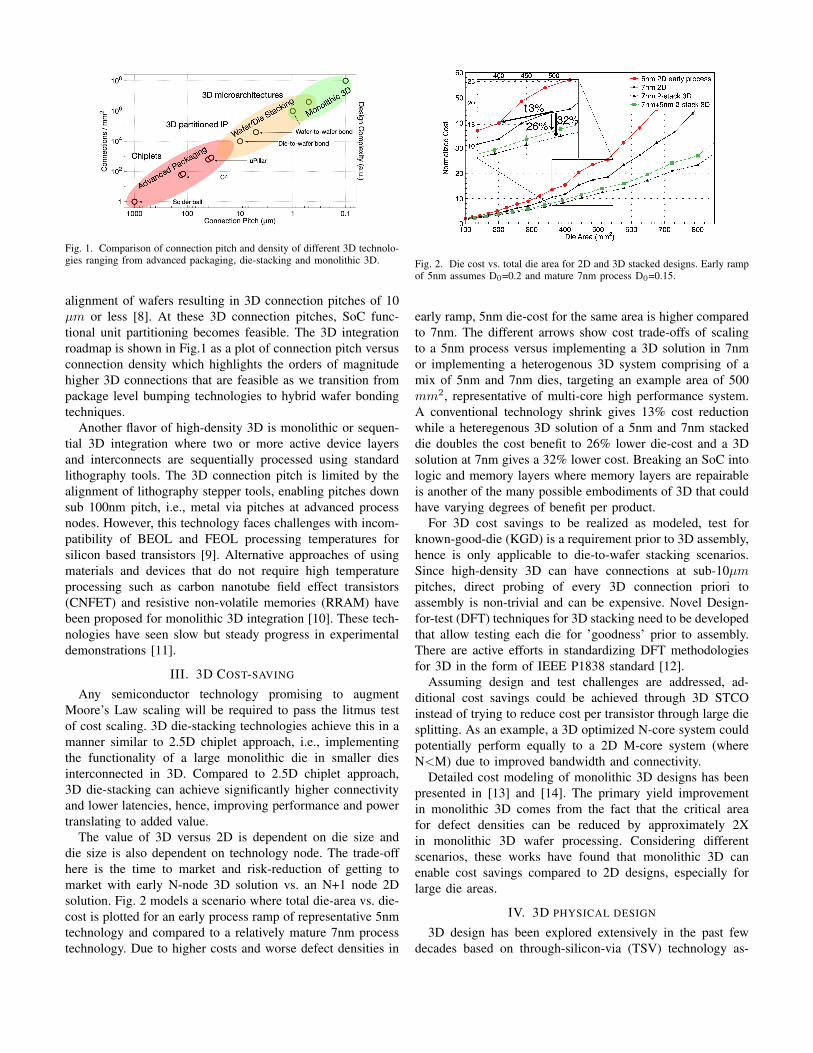
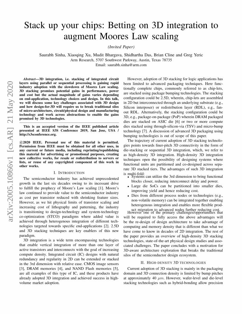
Fig. 1. Comparison of connection pitch and density of different 3D technolo-gies ranging from advanced packaging, die-stacking and monolithic 3D.
alignment of wafers resulting in 3D connection pitches of 10µm or less [8]. At these 3D connection pitches, SoC func-tional unit partitioning becomes feasible. The 3D integrationroadmap is shown in Fig.1 as a plot of connection pitch versusconnection density which highlights the orders of magnitudehigher 3D connections that are feasible as we transition frompackage level bumping technologies to hybrid wafer bondingtechniques.
Another flavor of high-density 3D is monolithic or sequen-tial 3D integration where two or more active device layersand interconnects are sequentially processed using standardlithography tools. The 3D connection pitch is limited by thealignment of lithography stepper tools, enabling pitches downsub 100nm pitch, i.e., metal via pitches at advanced processnodes. However, this technology faces challenges with incom-patibility of BEOL and FEOL processing temperatures forsilicon based transistors [9]. Alternative approaches of usingmaterials and devices that do not require high temperatureprocessing such as carbon nanotube field effect transistors(CNFET) and resistive non-volatile memories (RRAM) havebeen proposed for monolithic 3D integration [10]. These tech-nologies have seen slow but steady progress in experimentaldemonstrations [11].
III. 3D COST-SAVING
Any semiconductor technology promising to augmentMoore’s Law scaling will be required to pass the litmus testof cost scaling. 3D die-stacking technologies achieve this in amanner similar to 2.5D chiplet approach, i.e., implementingthe functionality of a large monolithic die in smaller diesinterconnected in 3D. Compared to 2.5D chiplet approach,3D die-stacking can achieve significantly higher connectivityand lower latencies, hence, improving performance and powertranslating to added value.
The value of 3D versus 2D is dependent on die size anddie size is also dependent on technology node. The trade-offhere is the time to market and risk-reduction of getting tomarket with early N-node 3D solution vs. an N+1 node 2Dsolution. Fig. 2 models a scenario where total die-area vs. die-cost is plotted for an early process ramp of representative 5nmtechnology and compared to a relatively mature 7nm processtechnology. Due to higher costs and worse defect densities in
Fig. 2. Die cost vs. total die area for 2D and 3D stacked designs. Early rampof 5nm assumes D0=0.2 and mature 7nm process D0=0.15.
early ramp, 5nm die-cost for the same area is higher comparedto 7nm. The different arrows show cost trade-offs of scalingto a 5nm process versus implementing a 3D solution in 7nmor implementing a heterogenous 3D system comprising of amix of 5nm and 7nm dies, targeting an example area of 500mm2, representative of multi-core high performance system.A conventional technology shrink gives 13% cost reductionwhile a heteregenous 3D solution of a 5nm and 7nm stackeddie doubles the cost benefit to 26% lower die-cost and a 3Dsolution at 7nm gives a 32% lower cost. Breaking an SoC intologic and memory layers where memory layers are repairableis another of the many possible embodiments of 3D that couldhave varying degrees of benefit per product.
For 3D cost savings to be realized as modeled, test forknown-good-die (KGD) is a requirement prior to 3D assembly,hence is only applicable to die-to-wafer stacking scenarios.Since high-density 3D can have connections at sub-10µmpitches, direct probing of every 3D connection priori toassembly is non-trivial and can be expensive. Novel Design-for-test (DFT) techniques for 3D stacking need to be developedthat allow testing each die for ’goodness’ prior to assembly.There are active efforts in standardizing DFT methodologiesfor 3D in the form of IEEE P1838 standard [12].
Assuming design and test challenges are addressed, ad-ditional cost savings could be achieved through 3D STCOinstead of trying to reduce cost per transistor through large diesplitting. As an example, a 3D optimized N-core system couldpotentially perform equally to a 2D M-core system (whereN<M) due to improved bandwidth and connectivity.
Detailed cost modeling of monolithic 3D designs has beenpresented in [13] and [14]. The primary yield improvementin monolithic 3D comes from the fact that the critical areafor defect densities can be reduced by approximately 2Xin monolithic 3D wafer processing. Considering differentscenarios, these works have found that monolithic 3D canenable cost savings compared to 2D designs, especially forlarge die areas.
IV. 3D PHYSICAL DESIGN
3D design has been explored extensively in the past fewdecades based on through-silicon-via (TSV) technology as-
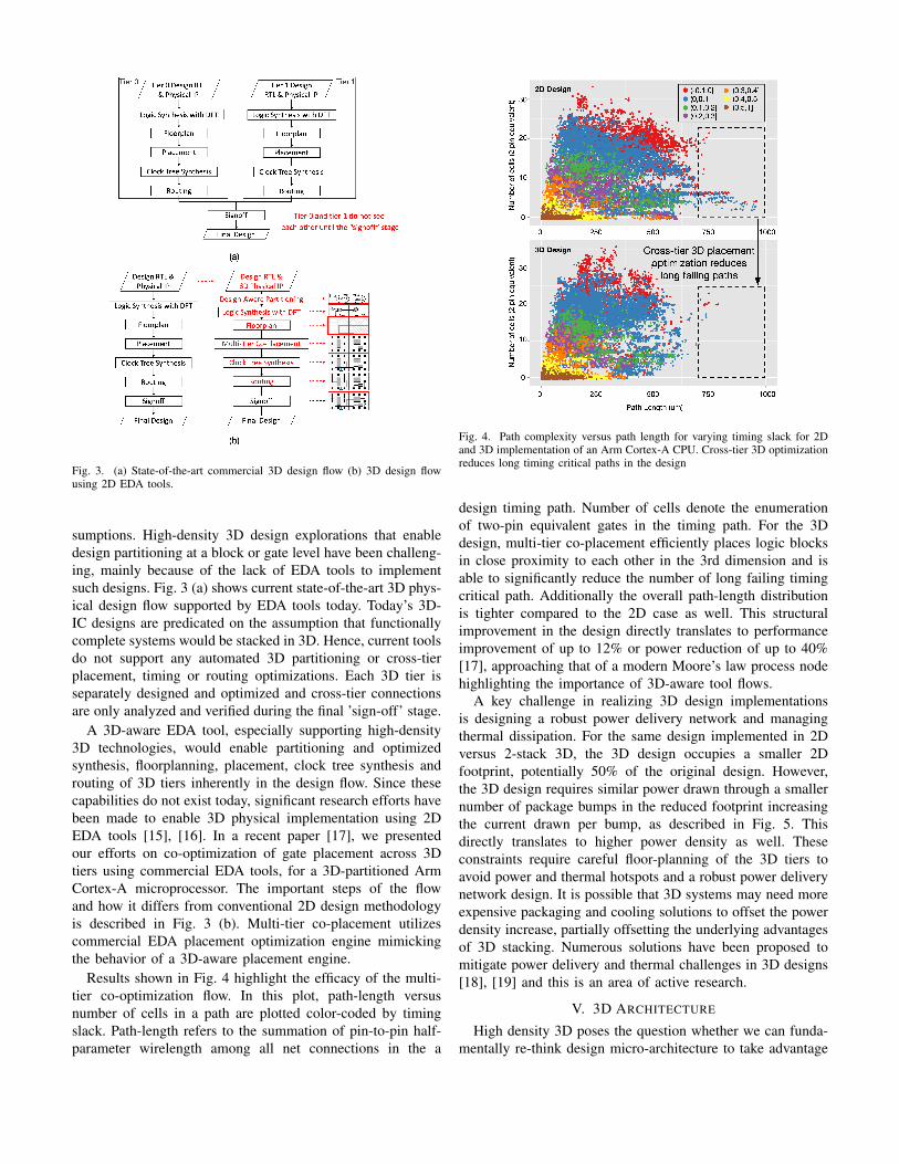
Fig. 3. (a) State-of-the-art commercial 3D design flow (b) 3D design flowusing 2D EDA tools.
sumptions. High-density 3D design explorations that enabledesign partitioning at a block or gate level have been challeng-ing, mainly because of the lack of EDA tools to implementsuch designs. Fig. 3 (a) shows current state-of-the-art 3D phys-ical design flow supported by EDA tools today. Today’s 3D-IC designs are predicated on the assumption that functionallycomplete systems would be stacked in 3D. Hence, current toolsdo not support any automated 3D partitioning or cross-tierplacement, timing or routing optimizations. Each 3D tier isseparately designed and optimized and cross-tier connectionsare only analyzed and verified during the final ’sign-off’ stage.
A 3D-aware EDA tool, especially supporting high-density3D technologies, would enable partitioning and optimizedsynthesis, floorplanning, placement, clock tree synthesis androuting of 3D tiers inherently in the design flow. Since thesecapabilities do not exist today, significant research efforts havebeen made to enable 3D physical implementation using 2DEDA tools [15], [16]. In a recent paper [17], we presentedour efforts on co-optimization of gate placement across 3Dtiers using commercial EDA tools, for a 3D-partitioned ArmCortex-A microprocessor. The important steps of the flowand how it differs from conventional 2D design methodologyis described in Fig. 3 (b). Multi-tier co-placement utilizescommercial EDA placement optimization engine mimickingthe behavior of a 3D-aware placement engine.
Results shown in Fig. 4 highlight the efficacy of the multi-tier co-optimization flow. In this plot, path-length versusnumber of cells in a path are plotted color-coded by timingslack. Path-length refers to the summation of pin-to-pin half-parameter wirelength among all net connections in the a
Fig. 4. Path complexity versus path length for varying timing slack for 2Dand 3D implementation of an Arm Cortex-A CPU. Cross-tier 3D optimizationreduces long timing critical paths in the design
design timing path. Number of cells denote the enumerationof two-pin equivalent gates in the timing path. For the 3Ddesign, multi-tier co-placement efficiently places logic blocksin close proximity to each other in the 3rd dimension and isable to significantly reduce the number of long failing timingcritical path. Additionally the overall path-length distributionis tighter compared to the 2D case as well. This structuralimprovement in the design directly translates to performanceimprovement of up to 12% or power reduction of up to 40%[17], approaching that of a modern Moore’s law process nodehighlighting the importance of 3D-aware tool flows.
A key challenge in realizing 3D design implementationsis designing a robust power delivery network and managingthermal dissipation. For the same design implemented in 2Dversus 2-stack 3D, the 3D design occupies a smaller 2Dfootprint, potentially 50% of the original design. However,the 3D design requires similar power drawn through a smallernumber of package bumps in the reduced footprint increasingthe current drawn per bump, as described in Fig. 5. Thisdirectly translates to higher power density as well. Theseconstraints require careful floor-planning of the 3D tiers toavoid power and thermal hotspots and a robust power deliverynetwork design. It is possible that 3D systems may need moreexpensive packaging and cooling solutions to offset the powerdensity increase, partially offsetting the underlying advantagesof 3D stacking. Numerous solutions have been proposed tomitigate power delivery and thermal challenges in 3D designs[18], [19] and this is an area of active research.
V. 3D ARCHITECTURE
High density 3D poses the question whether we can funda-mentally re-think design micro-architecture to take advantage
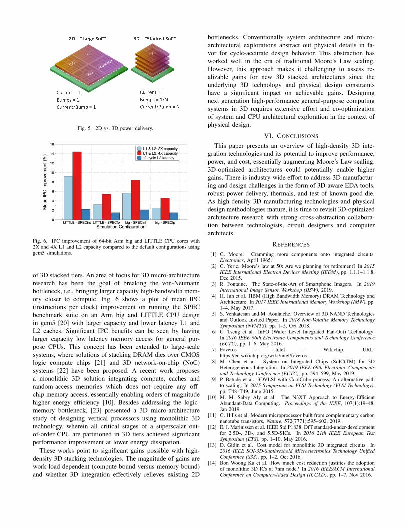
Fig. 5. 2D vs. 3D power delivery.
Fig. 6. IPC improvement of 64-bit Arm big and LITTLE CPU cores with2X and 4X L1 and L2 capacity compared to the default configurations usinggem5 simulations.
of 3D stacked tiers. An area of focus for 3D micro-architectureresearch has been the goal of breaking the von-Neumannbottleneck, i.e., bringing larger capacity high-bandwidth mem-ory closer to compute. Fig. 6 shows a plot of mean IPC(instructions per clock) improvement on running the SPECbenchmark suite on an Arm big and LITTLE CPU designin gem5 [20] with larger capacity and lower latency L1 andL2 caches. Significant IPC benefits can be seen by havinglarger capacity low latency memory access for general pur-pose CPUs. This concept has been extended to large-scalesystems, where solutions of stacking DRAM dies over CMOSlogic compute chips [21] and 3D network-on-chip (NoC)systems [22] have been proposed. A recent work proposesa monolithic 3D solution integrating compute, caches andrandom-access memories which does not require any off-chip memory access, essentially enabling orders of magnitudehigher energy efficiency [10]. Besides addressing the logic-memory bottleneck, [23] presented a 3D micro-architecturestudy of designing vertical processors using monolithic 3Dtechnology, wherein all critical stages of a superscalar out-of-order CPU are partitioned in 3D tiers achieved significantperformance improvement at lower energy dissipation.
These works point to significant gains possible with high-density 3D stacking technologies. The magnitude of gains arework-load dependent (compute-bound versus memory-bound)and whether 3D integration effectively relieves existing 2D
bottlenecks. Conventionally system architecture and micro-architectural explorations abstract out physical details in fa-vor for cycle-accurate design behavior. This abstraction hasworked well in the era of traditional Moore’s Law scaling.However, this approach makes it challenging to assess re-alizable gains for new 3D stacked architectures since theunderlying 3D technology and physical design constraintshave a significant impact on achievable gains. Designingnext generation high-performance general-purpose computingsystems in 3D requires extensive effort and co-optimizationof system and CPU architectural exploration in the context ofphysical design.
VI. CONCLUSIONS
This paper presents an overview of high-density 3D inte-gration technologies and its potential to improve performance,power, and cost, essentially augmenting Moore’s Law scaling.3D-optimized architectures could potentially enable highergains. There is industry-wide effort to address 3D manufactur-ing and design challenges in the form of 3D-aware EDA tools,robust power delivery, thermals, and test of known-good-die.As high-density 3D manufacturing technologies and physicaldesign methodologies mature, it is time to revisit 3D-optimizedarchitecture research with strong cross-abstraction collabora-tion between technologists, circuit designers and computerarchitects.
REFERENCES
[1] G. Moore. Cramming more components onto integrated circuits.Electronics, April 1965.
[2] G. Yeric. Moore’s law at 50: Are we planning for retirement? In 2015IEEE International Electron Devices Meeting (IEDM), pp. 1.1.1–1.1.8,Dec 2015.
[3] R. Fontaine. The State-of-the-Art of Smartphone Imagers. In 2019International Image Sensor Workshop (IISW), 2019.
[4] H. Jun et al. HBM (High Bandwidth Memory) DRAM Technology andArchitecture. In 2017 IEEE International Memory Workshop (IMW), pp.1–4, May 2017.
[5] S. Venkatesan and M. Aoulaiche. Overview of 3D NAND Technologiesand Outlook Invited Paper. In 2018 Non-Volatile Memory TechnologySymposium (NVMTS), pp. 1–5, Oct 2018.
[6] C. Tseng et al. InFO (Wafer Level Integrated Fan-Out) Technology.In 2016 IEEE 66th Electronic Components and Technology Conference(ECTC), pp. 1–6, May 2016.
[7] Foveros - Intel - Wikichip. URL:https://en.wikichip.org/wiki/intel/foveros.
[8] M. Chen et al. System on Integrated Chips (SoIC(TM) for 3DHeterogeneous Integration. In 2019 IEEE 69th Electronic Componentsand Technology Conference (ECTC), pp. 594–599, May 2019.
[9] P. Batude et al. 3DVLSI with CoolCube process: An alternative pathto scaling. In 2015 Symposium on VLSI Technology (VLSI Technology),pp. T48–T49, June 2015.
[10] M. M. Sabry Aly et al. The N3XT Approach to Energy-EfficientAbundant-Data Computing. Proceedings of the IEEE, 107(1):19–48,Jan 2019.
[11] G. Hills et al. Modern microprocessor built from complementary carbonnanotube transistors. Nature, 572(7771):595–602, 2019.
[12] E. J. Marinissen et al. IEEE Std P1838: DfT standard-under-developmentfor 2.5D-, 3D-, and 5.5D-SICs. In 2016 21th IEEE European TestSymposium (ETS), pp. 1–10, May 2016.
[13] D. Gitlin et al. Cost model for monolithic 3D integrated circuits. In2016 IEEE SOI-3D-Subthreshold Microelectronics Technology UnifiedConference (S3S), pp. 1–2, Oct 2016.
[14] Bon Woong Ku et al. How much cost reduction justifies the adoptionof monolithic 3D ICs at 7nm node? In 2016 IEEE/ACM InternationalConference on Computer-Aided Design (ICCAD), pp. 1–7, Nov 2016.
[15] S. Panth et al. Shrunk-2-D: A Physical Design Methodology toBuild Commercial-Quality Monolithic 3-D ICs. IEEE Transac-tions on Computer-Aided Design of Integrated Circuits and Systems,36(10):1716–1724, Oct 2017.
[16] K. Chang et al. Cascade2D: A design-aware partitioning approachto monolithic 3D IC with 2D commercial tools. In 2016 IEEE/ACMInternational Conference on Computer-Aided Design (ICCAD), pp. 1–8, Nov 2016.
[17] X. Xu et al. Enhanced 3D Implementation of an Arm R© Cortex R©-AMicroprocessor. In 2019 IEEE/ACM International Symposium on LowPower Electronics and Design (ISLPED), pp. 1–6, July 2019.
[18] M. Scheuermann et al. Thermal analysis of multi-layer functional3D logic stacks. In 2016 IEEE International 3D Systems IntegrationConference (3DIC), pp. 1–4, Nov 2016.
[19] K. Chang et al. System-Level Power Delivery Network Analysis andOptimization for Monolithic 3-D ICs. IEEE Transactions on Very LargeScale Integration (VLSI) Systems, 27(4):888–898, April 2019.
[20] N. Binkert et al. The Gem5 Simulator. SIGARCH Comput. Archit. News,39(2):1–7, August 2011.
[21] T. Carlson and M. Facchini. 3D Stacking of DRAM on Logic, pp. 187–210. Springer US, Boston, MA, 2011.
[22] I. Akgun et al. Network-on-Chip Design Guidelines for Monolithic 3DIntegration. IEEE Micro, pp. 1–1, 2019.
[23] B. Gopireddy and J. Torrellas. Designing Vertical Processors inMonolithic 3D. In Proceedings of the 46th International Symposium onComputer Architecture, ISCA ’19, pp. 643–656, New York, NY, USA,2019. ACM.