Embed Size (px)
Citation preview
ST7 FLASH STICKUser Manual
Release 1.2
October 2004
Ref: DOC-STICK-PP
INSTRUCTIONS FOR USE—WARNING
This product is conform to the 89/336/EEC Directive. It complies with the ITE EN55022 standard forEMC emissions and generic 50082-1 (1992 edition) immunity standards.
This product is an FCC Class-A apparatus. In a residential environment, it may causeradioelectrical disturbances.
In addition, this programming board is not contained in an outer casing; consequently, it cannot beimmune against electrostatic discharges (ESD). It should therefore be handled only in static safeworking areas. Please refer to Appendix A Safety Requirements on page 15 for relevant safetyinformation
USE IN LIFE SUPPORT DEVICES OR SYSTEMS MUST BE EXPRESSLY AUTHORIZED.
STMicroelectronics PRODUCTS ARE NOT AUTHORIZED FOR USE AS CRITICAL COMPONENTS INLIFE SUPPORT DEVICES OR SYSTEMS WITHOUT THE EXPRESS WRITTEN APPROVAL OFSTMicroelectronics. As used herein:
1. Life support devices or systems are thosewhich (a) are intended for surgical implant intothe body, or (b) support or sustain life, and whosefailure to perform, when properly used inaccordance with instructions for use providedwith the product, can be reasonably expected toresult in significant injury to the user.
2. A critical component is any component of a lifesupport device or system whose failure toperform can reasonably be expected to cause thefailure of the life support device or system, or toaffect its safety or effectiveness.
Table of Contents
3/26
Chapter 1: Introduction . . . . . . . . . . . . . . . . . . . . . . . . . . . . . . . . . . . . . . . . . . 4
1.1 About this manual... ...................................................................................... 51.2 Host PC system requirements ...................................................................... 6
1.3 Getting assistance ........................................................................................ 6
Chapter 2: Getting Started . . . . . . . . . . . . . . . . . . . . . . . . . . . . . . . . . . . . . . . . 7
2.1 Delivery checklist .......................................................................................... 7
2.2 Setting up the hardware ................................................................................ 7
2.3 In-circuit programming considerations .......................................................... 9
Chapter 3: Programming with STVD7 or STVP7 . . . . . . . . . . . . . . . . . . . . . 12
3.1 Start programming with STVD7 .................................................................. 12
3.2 Start programming with STVP7 .................................................................. 13
Appendix A Safety Requirements . . . . . . . . . . . . . . . . . . . . . . . . . . . . . . . . . . 15
Appendix B: Troubleshooting . . . . . . . . . . . . . . . . . . . . . . . . . . . . . . . . . . . . . . 16
B.1 Test pins ..................................................................................................... 16B.2 Error messages .......................................................................................... 17
B.3 “Problem on supply voltages” ..................................................................... 17
B.4 “Cannot communicate with the device” ....................................................... 18
Appendix C: Glossary . . . . . . . . . . . . . . . . . . . . . . . . . . . . . . . . . . . . . . . . . . . . 19
Appendix D: Schematics . . . . . . . . . . . . . . . . . . . . . . . . . . . . . . . . . . . . . . . . . . 21
Product Support . . . . . . . . . . . . . . . . . . . . . . . . . . . . . . . . . . . . . . . . . . . . . . . . . 23
Software updates ...................................................................................................... 23Hardware spare parts ............................................................................................... 23
Contact List ............................................................................................................... 24
Index . . . . . . . . . . . . . . . . . . . . . . . . . . . . . . . . . . . . . . . . . . . . . . . . . . . . . . . . . . . 25
1 - Introduction STICK User Manual
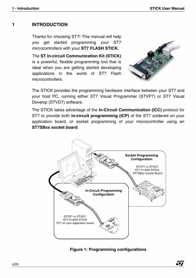
1 INTRODUCTION
The STICK provides the programming hardware interface between your ST7 andyour host PC, running either ST7 Visual Programmer (STVP7) or ST7 VisualDevelop (STVD7) software.
The STICK takes advantage of the In-Circuit Communication (ICC) protocol forST7 to provide both in-circuit programming (ICP) of the ST7 soldered on yourapplication board, or socket programming of your microcontroller using anST7SBxx socket board.
Thanks for choosing ST7! This manual will helpyou get started programming your ST7microcontrollers with your ST7 FLASH STICK.
The ST In-circuit Communication Kit (STICK)is a powerful, flexible programming tool that isideal when you are getting started developingapplications in the world of ST7 Flashmicrocontrollers.
Figure 1: Programming configurations
In-Circuit Programming Configuration
Socket Programming Configuration
STVP7 or STVD7,ST7 FLASH STICK
ST7 on your application board
STVP7 or STVD7,ST7 FLASH STICK,
ST7SBxx Socket Board
4/26
STICK User Manual 1 - Introduction
The STICK is delivered ”ready-to-use” for in-circuit programming of an MCU thathas been installed on a properly configured application board. However, socketprogramming of ST7 MCUs requires an additional ST7SBxx socket board. Formore information about socket programming with the STICK, you can refer to theST7SBxx Socket Board User Guide.
1.1 About this manual...
This manual will help you set up your STICK programming tool and connect it toyour PC. Here you will find:
• Setup instructions
• Detailed hardware information
• A trouble shooting guide for your programming tool
For more information about the hardware and software intended for use with yourSTICK, refer to the following documents:
ST7 Visual Programmer online help– information about the STVP7 programminginterface
ST7 Visual Develop User Manual– information about the STVD7 programminginterface
ST7SBxx Socket Board User Guide– setup information for socket programming
ST7xxxx Datasheet– includes information about ICC connection and micro-controller programming that is specific to your MCU
1.1.1 Revision history
Date Revision Description
Nov 2000 1.1 • Updated Section 1.2 – includes support of windows XP
Jun 2001 1.2 • Added Table 1 – Revision history table
• Added Section 2.3 – setting up ICP connection
• Added Section 3.1 – programming from STVD7
Table 1: STICK User Manual Revision History
5/26
1 - Introduction STICK User Manual
1.2 Host PC system requirements
Both hardware and software components of the STICK have been designed towork with PCs meeting the following requirements:
• One of the following operating systems: Microsoft® Windows® 98, 2000,
Millennium, NT® or XP®.
• Intel® Pentium (or compatible) processor with minimum speed of 133 MHz.
• Minimum RAM of 32 MB (64 MB recommended).
• 50 MB of free hard disk space to install all of the ST7 tools.
• Parallel port
Note: Windows® 2000, NT® and XP users must have administrator privileges to install the requiredsoftware.
1.3 Getting assistance
For more information, application notes, FAQs and software updates on all the STmicrocontroller families, check the CD-ROM or our website:
www.st.com/mcu
For assistance on all ST microcontroller subjects, for help using your programmingtools, refer to the contact list provided in Product Support on page 23. We’ll be gladto help you!
6/26
STICK User Manual 2 - Getting Started
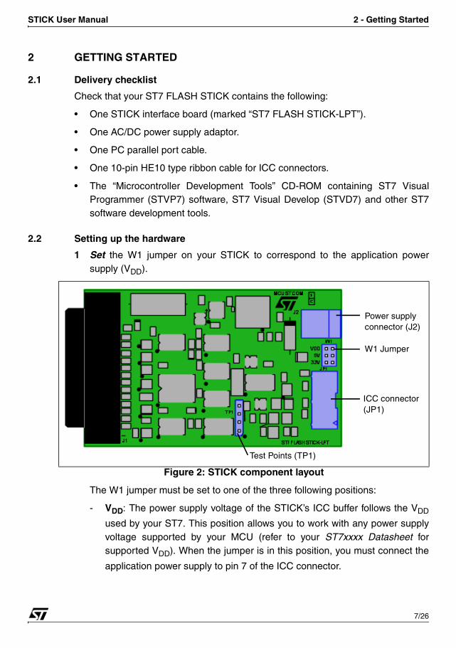
2 GETTING STARTED
2.1 Delivery checklist
Check that your ST7 FLASH STICK contains the following:
• One STICK interface board (marked “ST7 FLASH STICK-LPT”).
• One AC/DC power supply adaptor.
• One PC parallel port cable.
• One 10-pin HE10 type ribbon cable for ICC connectors.
• The “Microcontroller Development Tools” CD-ROM containing ST7 VisualProgrammer (STVP7) software, ST7 Visual Develop (STVD7) and other ST7software development tools.
2.2 Setting up the hardware
1 Set the W1 jumper on your STICK to correspond to the application powersupply (VDD).
The W1 jumper must be set to one of the three following positions:
- VDD: The power supply voltage of the STICK’s ICC buffer follows the VDD
used by your ST7. This position allows you to work with any power supplyvoltage supported by your MCU (refer to your ST7xxxx Datasheet forsupported VDD). When the jumper is in this position, you must connect the
application power supply to pin 7 of the ICC connector.
Figure 2: STICK component layout
Power supply connector (J2)
W1 Jumper
ICC connector (JP1)
Test Points (TP1)
7/26
2 - Getting Started STICK User Manual
- 5 V: The power supply voltage of the STICK’s ICC buffer is 5 V. You don’tneed to connect the application VDD to pin 7 of the ICC connector, but your
application must be powered by 5 V +/- 5%.
- 3.3 V: The power supply voltage of the STICK’s ICC buffer is 3.3 V. Youdon’t need to connect the application VDD to pin 7 of the ICC connector, but
your application must be powered by 3.3 V +/- 5%.
2 Connect the STICK to the parallel port of your host PC with the suppliedparallel cable.
Note: Be sure to use the provided PC parallel port cable—using a longer cable may causemalfunctions. Connect the cable directly between the host PC and the STICK—usingadditional cables or switch boxes between the host PC and the STICK may causemalfunctions.If a dongle is already connected to the PC’s parallel port, it should not interfere with theSTICK. However, if your STICK malfunctions, remove the dongle and restart the setup.
3 Power on the STICK using the provided AC/DC power supply, which you pluginto the J2 connector. Ensure that the power supply is adapted to the mainsvoltage and outlet type used in your country.
4 Connect the ICC cable to the ICC connectors on your STICK (JP1) and yourapplication board (for more information about installing an ICC connector onyour application board, refer to Section 2.3).
5 Power up your application board.
You are now ready to program your ST7. For more information about theprogramming sequence, refer to Chapter 3: Programming with STVD7 or STVP7on page 12, or refer to your software’s on-line help file.
8/26
STICK User Manual 2 - Getting Started
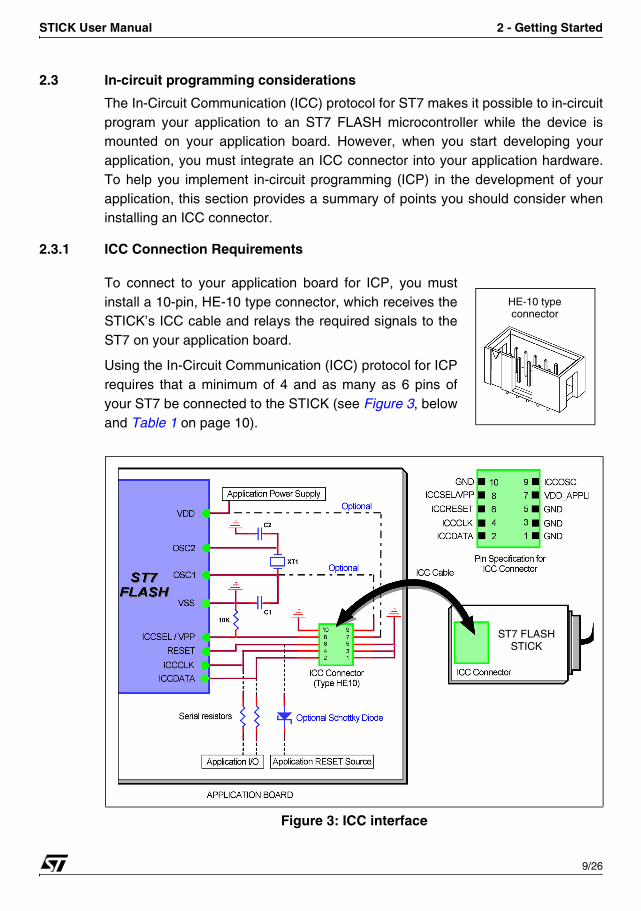
2.3 In-circuit programming considerations
The In-Circuit Communication (ICC) protocol for ST7 makes it possible to in-circuitprogram your application to an ST7 FLASH microcontroller while the device ismounted on your application board. However, when you start developing yourapplication, you must integrate an ICC connector into your application hardware.To help you implement in-circuit programming (ICP) in the development of yourapplication, this section provides a summary of points you should consider wheninstalling an ICC connector.
2.3.1 ICC Connection Requirements
To connect to your application board for ICP, you mustinstall a 10-pin, HE-10 type connector, which receives theSTICK’s ICC cable and relays the required signals to theST7 on your application board.
Using the In-Circuit Communication (ICC) protocol for ICPrequires that a minimum of 4 and as many as 6 pins ofyour ST7 be connected to the STICK (see Figure 3, belowand Table 1 on page 10).
Figure 3: ICC interface
HE-10 type connector
ST7 FLASH STICK
9/26
2 - Getting Started STICK User Manual
Isolation of ICCDATA and ICCCLK pins
As soon as your STICK is plugged into the application board the ICCDATA andICCCLK pins must not be used by other application devices, even if you are notprogramming your MCU. If the application uses these pins as inputs, isolation suchas a serial resistor must be implemented to prevent other application devices fromforcing a signal on either of these pins. The application board must not drivecurrent in excess of 1mA.
If the ICCDATA and ICCCLK pins are only used as outputs by the application, nosignal isolation is necessary.
For ST7 MCUs with no ICCSEL pin, during normal operation the ICCCLK pin mustbe pulled-up internally or externally (10KΩ pull-up required in noisy environments).This is to avoid entering ICC mode unintentionally during a reset. For moreinformation, refer to the ST7 ICC Protocol Reference Manual.
Isolation of the RESET pin
During a programming session, you must ensure that the programming toolcontrols the ST7’s RESET pin so that no external reset is generated by theapplication. This can lead to a conflict if the application reset circuitry signalexceeds 5mA (push-pull output or pull-up resistor <1k). To avoid such conflicts, aShottky diode can be used to isolate the application reset circuit.
ST7 pin Connects to
ICCDATA ICC input serial data pin ICCDATA
ICCCLK ICC output serial clock pin ICCCLK
RESET Device reset ICCRESET
ICCSEL/VPP Programming voltage ICCSEL/VPP
OSC1 or OSCIN * Main clock input for external ICCOSC
VDD * Device power supply VDD_APPLI
VSS Device power supply (ground) GND
* Optional connection for the STICK, see text.
Table 1: ICC connection requirements
10/26
STICK User Manual 2 - Getting Started
ICCSEL/VPP pin
The application pull-down resistor must not be lower than 10kΩ.
ICCOSC pin *
The ICCOSC pin of the ICC connector must be connected to the ST7’s OSC1 orOSCIN pin if the clock is not provided by the application, or if the application clocksource is not programmed in the option byte. This connection allows you to startyour ICP session using the ICP OPT Disable programming mode. In this mode,the STICK provides a clock source to initiate communication with the ST7 at afrequency of 8MHz.
For ST7 devices with multi-oscillator capability, when the ICCOSC pin isconnected, the OSC2 pin should be grounded.
If your application provides a clock signal and you are certain that it is programmedin the ST7’s option byte, you can start your ICP session using the ICP OPT Enableprogramming mode. In this mode, your application clock source provides the clocksignal for initiating communication with your ST7 and ICCOSC is not connected toyour ST7.
VDD_APPLI pin *
This pin is used by the programming tool’s power supply follower, which adapts thevoltage of the tool’s signals to your application’s VDD. If the application board VDDis equal to 5v or 3.3v, VDD_APPLI is not connected. However, the W1 jumper mustbe set to the appropriate position (5v or 3.3v). For all other VDD values supportedby your ST7 (refer to your ST7xxxx Datasheet), this pin must be connected and theW1 jumper set to the VDD position.
11/26
3 - Programming with STVD7 or STVP7 STICK User Manual
3 PROGRAMMING WITH STVD7 OR STVP7
You can configure and control the programming of your ST7 with ST7 VisualProgrammer (STVP7) or ST7 Visual Develop (STVD7) software running on yourhost PC. This chapter provides a brief procedure to help you get startedprogramming with each software. For more details refer to their respective on-linehelp files.
3.1 Start programming with STVD7
1 Launch STVD7.
2 Open the workspace and project that you used when developing yourapplication. You will have selected your MCU during the early stages ofapplication development.
3 Select Tools>Programmer.
4 Configure the options in the Settings tab:
- Board: STICK
- Port: LPT1 or LPT2
- Check Erase Before Programming if you are reprogramming an MCUwith HDFlash memory.
- Programming Mode:
If your ST7’s option byte does not include OSCTYPE, then ICP is the onlyin-circuit programming mode available to you.
Note: For some of the most recent circuits that include OSCTYPE, ICP programming mode isavailable instead of ICP OPT Disable or Enable.
If your ST7’s option byte includes OSCTYPE, then you can choose:
ICP OPT Disable– a safe mode that must be used if your application clockcircuitry doesn’t match the OSCTYPE option byte selection. In this mode,an external source with a square wave signal from 0 V to VDD must be
provided either by the STICK via the ICC connector pin 9 (ICCOSC safeclock), or your application.
ICP OPT Enable– used only if your application clock circuitry matches theOSCTYPE option byte selection. In this case, the ICC connector pin 9 isnot connected and the ICCOSC safe clock is not used.
5 Power on your application board and connect the ICC cable between yourSTICK and the application.
12/26
STICK User Manual 3 - Programming with STVD7 or STVP7
6 Select the Memory Area tab then select a memory area. Click on Add, thenuse the browse window to identify the file (.s19, .hex) to program the selectedmemory area with. Repeat this step as necessary for each memory area.
7 Select the Option Byte tab to configure any option byte settings.
8 Select the Program tab and click on Start to program your ST7.
3.2 Start programming with STVP7
The following describes a basic procedure for programming your application toyour MCU without creating a project in STVP7.
Note: Setting up a project is a way of configuring STVP7 so that you can use the sameconfiguration each time you run STVP7. For more information about projects, refer toSTVP7’s on-line help.
1 Launch STVP7
2 In the Configuration window specify:
- Hardware: STICK
- Port: LPT1 or LPT2
- Programming mode:
Select ICP mode if your ST7’s option byte does not include OSCTYPE. TheDevice field will change to show the list of devices that only use this mode.
Note: For some of the most recent circuits that include OSCTYPE, ICP programming mode isavailable instead of ICP OPT Disable or Enable.
If your ST7’s option byte does include OSCTYPE, you can choose one ofthe following options:
ICP OPT Disable– a safe mode that must be used if your application clockcircuitry doesn’t match the OSCTYPE option byte selection. In this mode,an external source with a square wave signal from 0 V to VDD must be
provided either by the STICK via the ICC connector pin 9 (ICCOSC safeclock), or your application.
ICP OPT Enable– used only if your application clock circuitry matches theOSCTYPE option byte selection. In this case, the ICC connector pin 9 isnot connected and the ICCOSC safe clock is not used.
When you choose one of the modes, the Device field will display the list ofdevices that support these modes.
13/26
3 - Programming with STVD7 or STVP7 STICK User Manual
- Device:
Select the name of your MCU from the list in the Device field. Keep in mindthat the list displayed for ICP mode is different from that displayed for theother two in-circuit programming modes.
3 Erase memory before reprogramming (HDFlash only) by selectingErase>Active sector(s). If you want the memory to be erased systematicallybefore programming, you can activate the Erase Device Memory BeforeProgramming feature (Edit>Preferences).
4 Select files (.s19, .sx, .hex) for programming to memory areas. Select the tabfor the memory area (for example, PROGRAM MEMORY or DATA MEMORY),then select File>Open. Locate the file using the resulting browse window andclick on Open.
5 Select the Option Byte tab. Option bytes can be configured using the list boxesin this tab or by loading a HEX or S19 file with the previously used option bytesettings. To program option bytes from a file, select the Option Byte tab, thenclick on File>Open to load the file containing the option byte settings.
6 Program your ST7 by selecting Program>All Tabs (on active sectors, if any).
7 Check the content by selecting Verify>All Tabs (on active sectors, if any). Ifyou want to check the programmed content systematically after programming,ensure that the Verify After Programming feature is activated(Edit>Preferences)
14/26

STICK User Manual Appendix A Safety Requirements
15/26
APPENDIX A SAFETY REQUIREMENTS
• Any tester, equipment, or tool used at any production step, or for anymanipulation of semiconductor devices, have its shield connected to ground.
• The product must be placed on a conductive table top, made of steel or cleanaluminum, or covered by an antistatic surface (superficial resistivity equal to or
higher than 0.5 MΩ/cm2), grounded through a ground cable (conductive cablefrom protected equipment to ground isolated with a 1 MΩ resistor placed inseries). All manipulation of finished goods must be done at such a groundedworktable.
• The worktable free of all non-antistatic plastic objects.
• An antistatic floor covering grounded through a conductive ground cable (withserial resistor between 0.9 and 1.5 MΩ) should be used.
• It is recommended that you wear an antistatic wrist or ankle strap, connected tothe antistatic floor covering or to the grounded equipment.
• If no antistatic wrist or ankle strap is worn, before each manipulation of thepowered-on tool, you touch the surface of the grounded worktable.
• It is recommended that antistatic gloves or finger coats be worn.
• It is recommended that nylon clothing be avoided while performing anymanipulation of parts.
Appendix B: Troubleshooting STICK User Manual
APPENDIX B: TROUBLESHOOTING
This appendix covers some of the problems that may occur, and how to solvethem.
B.1 Test pins
The STICK is equipped with test pins located at TP1 (see board layout in Figure 2on page 7). If you have problems with programming, these pins can help youpinpoint anomalies in the ICC communication by testing or checking the ICCsignals.
Pin Signal Description
1 GND This pin is marked with a white dot.
2 Power The external power supply value can be checked here. It is an unregulated 12 V DC power supply. Its value should be in the range 13.5 V to 23 V depending on the current load.
3 VCC The VCC is regulated at 5 V +/- 5%.
4 VCC_a This is the operational amplifier output that follows the voltage value selected by the W1 jumper. It should be equal to:
• your application VDD voltage value if W1 is inthe VDD position,
• 5 V if W1 is in the 5 V position,• 3.3 V if W1 is in the 3.3 V position.
5 ICCSEL_VPP This signal may be at 0 V, 5 V or 12 V. This test point is used during factory test. You do not have to check it.
Table 1 Test pins
16/26
STICK User Manual Appendix B: Troubleshooting
B.2 Error messages
The following sections explain the cause of some common error messages.
B.2.1 “PC parallel port cable not connected”
Most communication failures between the host PC and the STICK stem fromproblems in the parallel port connection. To prevent communication problems,when setting up your parallel port connection:
• Use the parallel cable provided with your STICK—using a longer parallel cablemay cause malfunctions.
• Connect the cable directly between the host PC and STICK interface board—the insertion of additional cables or switch boxes between the host PC and theinterface board may cause malfunctions.
• Remove any parallel port dongles.
• Ensure that the parallel port address is in the range 03BC-03BF or 0378-037For 0278-027F.
• Ensure that the parallel port is not disabled in your PC. For example, in the
IBM® ThinkPad™, you can select “infrared printing (LPT) port on”.
B.3 “Problem on supply voltages”
When you have supply voltage problems the green LED will not come on. To findthe cause of the problem:
• Check that the AC/DC power supply adaptor is firmly connected to both themain power supply and to the STICK interface board. To check that the mainpower supply is on, disconnect the ICC cable and measure the voltage on testpin 2 of TP1 (see Test pins on page 16). This pin should have an unregulatedDC value in the range 18 V to 21 V.
Note: Ground is on TP1 pin 1 (white dot mark).
• Check that the W1 jumper is set to one of the three positions, see Section 2.2on page 7. If it is set on the “VDD” position, check that the ICC cable isconnected properly and that your application’s VDD is connected to ICCconnector pin 7. Your application VDD must be in the range 2.4 V to 5 V. Thevoltage measured on test pin 4 of TP1 (see Test pins on page 16), must be thesame voltage value that you selected with the W1 jumper.
• Check that there is 5 V on test pin 3 of TP1 (see Test pins on page 16).
17/26
Appendix B: Troubleshooting STICK User Manual
If you have made all of these checks and you still get the “Problem on supplyvoltages” message, contact your ST distributor or sales office (see ProductSupport on page 23) in order to have your STICK repaired.
B.4 “Cannot communicate with the device”
Check that:
• The ICC cable is correctly connected.
• You have selected the right ST7 device.
• The ICC signals are clear and within the following ranges:
- ICCDATA: This application signal must not drive more than 1 mA.
- ICCCLK: This application signal must not drive more than 1 mA.
- ICCRESET: This application signal must not drive more than 5 mA.
- ICCSEL_VPP: The pull-down resistor must not be lower than 10 kOhm.
• You have selected the right programming mode (see Chapter 3 on page 12).Remember that:
- If you use ICP OPT Enable mode, check that your application clockcircuitry does match the CLOCK SOURCE and OSCTYPE options alreadyprogrammed in the ST7 Flash microcontroller option byte. For devices outof factory you have to check these values in datasheet. If you don’t knowthese values you have to select ICP OPT Disable.
- ICP OPT Disable mode, ensure that external source clock is a squarewave signal from 0 V to VDD. If not, you have to connect ICCOSC safeclock (ICC connector pin 9) to the OSC1 pin of the ST7Flashmicrocontroller in your application
18/26
STICK User Manual Appendix C: Glossary
APPENDIX C: GLOSSARY
This appendix gives a brief definition of acronyms and names used in this manual.
HDFlash
High density FLASH memory is based on FLASH technology. HDFlash is used formicrocontrollers with 4K up to 60Kbytes of FLASH memory. It is programmed byteby byte but erased by sector.
ICC protocol
In-Circuit Communication protocol is a way of exchanging data between anST7 Flash microcontroller and an external system (i.e. PC) using minimumhardware and ST7 I/Os in the user application. In the ST7 Flash microcontrollers,this protocol is handled by the ICC monitor.
ICC monitor
Software that handles the ICC protocol, embedded in a reserved memory area ofthe ST7 Flash microcontroller. At RESET, using specific signal sequence, the ST7jumps to this ICC monitor which allows it to download programs in RAM and toexecute them. This feature is used to implement the ICP functionality.
In-Circuit Programming (ICP)
This is programming the ST7 FLASH memory while ST7 Flash microcontroller isplugged into the application board.
In-Circuit Testing (ICT)
This is testing ST7 Flash micro and/or your application through the ST7 Flashmicrocontroller while it is plugged into the application board.
In-Circuit Debugging (ICD)
This is debugging your application while the ST7 Flash microcontroller is pluggedinto the application board.
ST7 Flash microcontroller
An ST7 microcontroller with electrically erasable memory that can be either XFlashor HDFlash memory.
STICK
ST In-circuit Communication Kit.
19/26
Appendix C: Glossary STICK User Manual
XFlash
Extended FLASH memory is based on EEPROM technology. XFlash providesextended features such as byte re-programming (by means of byte erasing) anddata EEPROM capability. XFlash microcontrollers are available between 1K to16 Kbytes.
20/26
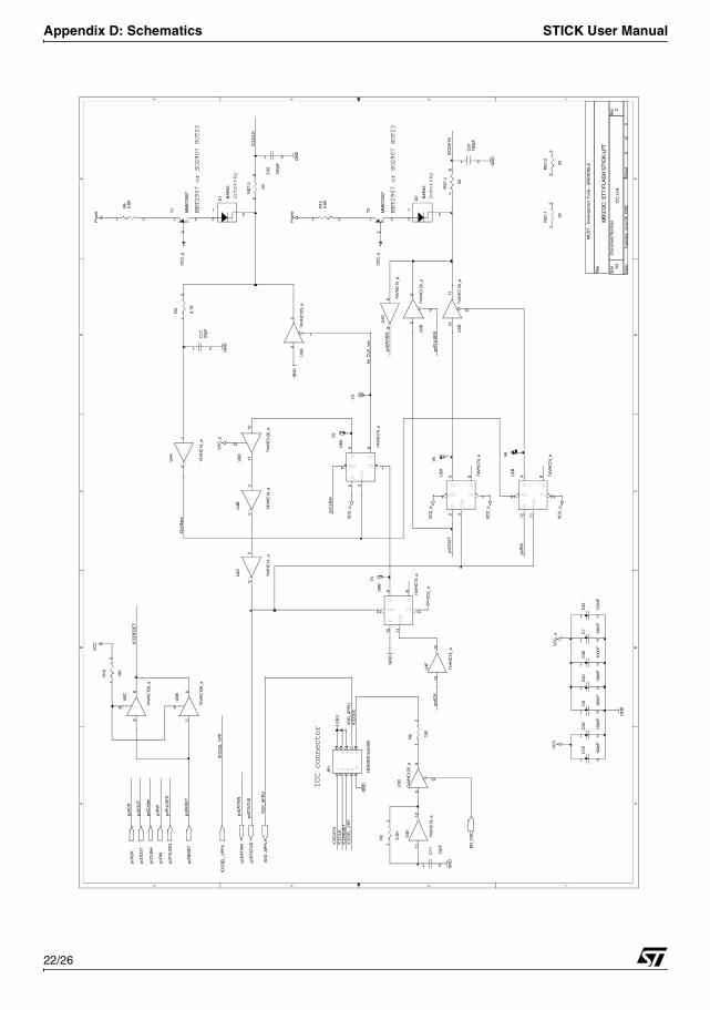
STICK User Manual Appendix D: Schematics
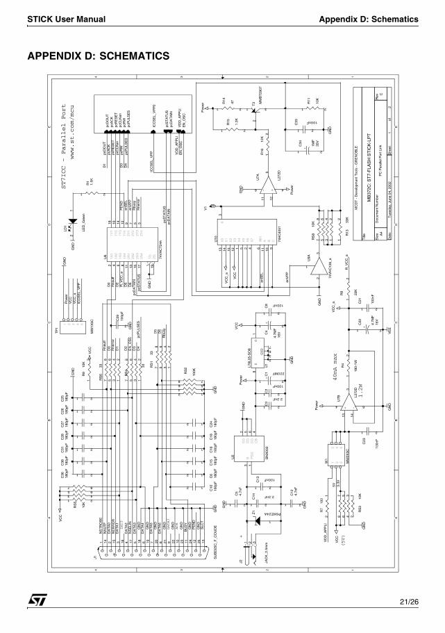
APPENDIX D: SCHEMATICSA A
B B
C C
D D
E E
44
33
22
11
DATA7
1.2W
40mA max
(5V)
ST7ICC - Parallel Port
www.st.com/mcu
+
35V
16V
16V
INIT
ACK
PC
Par
alle
l Por
t Lin
kC
MB
372C
: ST
7-F
LAS
H S
TIC
K-L
PT
A4
12
Tue
sday
, Jun
e 04
, 200
2
MC
DT
- D
evel
opm
ent T
ools
- G
RE
NO
BLE
Titl
e
Siz
eD
ocum
ent N
umbe
rR
ev
Dat
e:S
heet
of
pcD
AT
AIN
pcA
CK
pcD
OU
T
pcP
ULS
ES
pcR
Wpc
CLK
en
pcS
TA
TU
S
pcR
ES
ET
ICC
SE
L_V
PP
0
VD
D_A
PP
LIE
N_O
SC
Rne
rror
D2
D0
R_V
CC
_aD
5
pcD
OU
TD
1
Rbu
sy
pcC
LKen
pcA
CK
VD
D_A
PP
LI
pcP
ULS
ES
D4
D6
enS
EL
pcS
TA
TU
S
pcD
AT
AIN
pcD
AT
AIN
pcR
ES
ET
pcS
TA
TU
S
3.3V
enV
PP
enV
PP
enS
EL
EN
_OS
C
D1
Rna
utf
D5
D2
Rbu
syD6
EN
_OS
C
D3
Rne
rror
D4
pcP
ULS
ES
D0
Rna
utf
5V
Pow
erV
CC
VC
C_a
ICC
SE
L_V
PP
ICC
SE
L_V
PP
VD
D_A
PP
LI
D3
pcR
W
R_V
CC
_a
PE
ND
NS
TR
OB
E
NS
ELI
N
GN
D
GN
D
DA
TA
2
DA
TA
5
DA
TA
0
DA
TA
6G
ND
GN
DB
US
Y
GN
D
GN
D
GN
D
DA
TA
1
PE
ND
NE
RR
OR
DA
TA
3
DA
TA
4
GN
D
NA
UT
F
SLC
T
GN
D
GN
D
Pow
er
GN
D
VC
C
GN
D
VE
E
VC
C
VC
C_a
Pow
er
VC
C_a
VC
C
GN
D
VC
C
GN
D
GN
D
GN
D
GN
D
Pow
er
Pow
er
GN
D
GN
D
GN
D
GN
D
GN
D
GN
D
VC
C
GN
DC
3118
0pF
1 2
U10
74H
C40
51
13 14 15 121 5 2 4 6
11 109
3X
0X
1X
2X
3X
4X
5X
6X
7
INH
A B C
X
C33 100nF
1 2
C5
4.7n
F
1 2
R7
100
12
J1 SU
BD
25C
_F_C
OU
DE
13251224112310229218207196185174163152141
+-
U7A
L272
D
12115
46
C21
100n
F
1 2
V1
R9
10K
12
+C
4
4.7M
F
1 2
RS
133
26
1357
48
RS
4
3326
1357
48
LD1
LED
_Gre
en
12
C23
100n
F
1 2
U9A
74V
HC
126_
a
23
1
C25
180p
F
1 2
R8
22K
12
C14 2.2nF
1 2
C18
180p
F
12
I
GND
O
U1
L78L
05-S
O8
8
2
1
367
C12
4.7n
F
1 2
C2
100nF
1 2
C28
180p
F
1 2
W1
MW
2X3C
12
34
56
RS
2
100K
2
6
1357
4
8
J2 JAC
K_2
.5m
m2 31
+ -
U7B L2
72D
13 143
4 6
U6
74V
HC
T24
4
2 4 6 811 13 15 17
119
18 16 14 12 9 7 5 3
1A1
1A2
1A3
1A4
2A1
2A2
2A3
2A4
1G 2G
1Y1
1Y2
1Y3
1Y4
2Y1
2Y2
2Y3
2Y4
C3
2.2nF
1 2
+C
34
1MF
1 2
C24
180p
F
12
C29
100p
F
1 2
R14
47
1 2
R16
12K
12
R1
1.5K
1 2
C13 100nF
1 2
C6
180p
F
12
RS
5
10K
2
6
1357
4
8
Z1 P6KE24A
12
RS
810
K
26
1357
48
C8 100nF
1 2
C36
180p
F
1 2
C27
180p
F
1 2
+C
1 220MF
1 2
C10
180p
F
12
T3 M
MB
T29
07
2
1 3
RS
633
26
1357
48
TP
1
MW
1X5C1 2 3 4 5
R4
180-
1W
12
R11
10K
1 2
RS
310
K
26
1357
48
+C
22
4.7M
F
1 2
C38
180p
F
1 2
C15
180p
F
12
R13
33K
12
C26
180p
F
1 2
R15
1.2K
1 2
U2
BN
X00
2
3 1
2 5 6 4
B PS
G
CG
CG
CG
CB
C16
180p
F
12
21/26
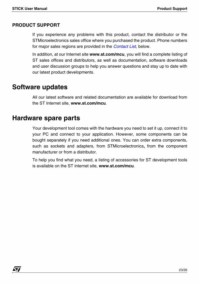
Appendix D: Schematics STICK User Manual
A A
B B
C C
D D
E E
44
33
22
11
MBT2907 or SO2907 SOT23
Schottky
Schottky
MBT2907 or SO2907 SOT23
ICC connector
ICC
Lin
kC
MB
372C
: ST
7-F
LAS
H S
TIC
K-L
PT
A3
22
Tue
sday
, Jun
e 04
, 200
2
MC
DT
- D
evel
opm
ent T
ools
- G
RE
NO
BLE
Titl
e
Siz
eD
ocum
ent N
umbe
rR
ev
Dat
e:S
heet
of
pcD
AT
AIN
pcC
LKen
pcA
CK
pcD
OU
T
pcR
W
CLK
INic
c
pcD
AT
AIN
pcA
CK
pcC
LKen
pcP
ULS
ES
pcP
ULS
ES
pcR
W
pcD
OU
T
pcS
TA
TU
S
VD
D_A
PP
LI
ICC
SE
L_V
PP
tie_C
LK_l
ow
pcR
ES
ET
ICC
OS
C
ICC
RE
SE
TIC
CC
LK
ICC
SE
L_V
PP
VD
D_A
PP
LI
ICC
DA
TA
ICC
DA
TA
ICC
CLK
ICC
RE
SE
T
GN
D
GN
D
GN
D
VC
C
VC
C_a
GN
D
VC
C_a
VC
C_a
Pow
er
GN
D
VC
C_a
VC
C_a
VC
C_a
VC
C_a
VC
C_a
VC
C_a
Pow
er
VC
C
GN
D
GN
D
GN
D
GN
D
U9C
74V
HC
126_
a
98
10
RS
7-1
33
12
V5
JP1
HE
AD
ER
5x2
/SM
12
34
56
78
910
U4E
74V
HC
14_a
1110
C35
180p
F
1 2
V3
C39
100n
F
1 2
T2
MM
BT
2907
2
1 3
U4C
74V
HC
14_a
56
RS
7-4
33
78
D2 BA
R42
23
1
RS
7-2
33
34
R6 10
0
12
U9D
74V
HC
126_
a1211
13
U4D
74V
HC
14_a
98
U3B
74V
HC
125_
a
56
4
V2
V4
C20
100n
F
1 2
D1 BA
R42
23
1
V6
U4A
74V
HC
14_a
12
U5A
74V
HC
74_a
2 3
5 6
4 1
D CLK
Q Q
PR CL
C37
180p
F
1 2
U8B
74V
HC
74_a
12 11
9 8
10 13
D CLK
Q Q
PR CL
C7
100n
F
1 2
C19
100n
F
1 2
R5
5.6K
1 2
C17
22pF
1 2
T1
MM
BT
2907
2
1 3
RS
7-3
33
56
U3C
74V
HC
125_
a
98
10
C9
100n
F
1 2
R2
3.3K
12
C11
33pF
1 2
R10
10K
12
U9B
74V
HC
126_
a
56
4
U3D
74V
HC
125_
a
1211
13
R3
4.7K
12
U4B
74V
HC
14_a
34
U3A
74V
HC
125_
a
23
1
U8A
74V
HC
74_a
2 3
5 6
4 1
D CLK
Q Q
PR CL
C32
100n
F
1 2
U5B
74V
HC
74_a
12 11
9 8
10 13
D CLK
Q Q
PR CL
R12
5.6K
1 2
U4F
74V
HC
14_a
1312
C30
100n
F
1 2
pcA
CK
pcD
OU
T
pcC
LKen
pcR
W
pcS
TA
TU
S
pcP
ULS
ES
pcR
ES
ET
pcD
AT
AIN
ICC
SE
L_V
PP
0
VD
D_A
PP
LI
EN
_OS
C
22/26
STICK User Manual Product Support
PRODUCT SUPPORT
If you experience any problems with this product, contact the distributor or theSTMicroelectronics sales office where you purchased the product. Phone numbersfor major sales regions are provided in the Contact List, below.
In addition, at our Internet site www.st.com/mcu, you will find a complete listing ofST sales offices and distributors, as well as documentation, software downloadsand user discussion groups to help you answer questions and stay up to date withour latest product developments.
Software updatesAll our latest software and related documentation are available for download fromthe ST Internet site, www.st.com/mcu.
Hardware spare partsYour development tool comes with the hardware you need to set it up, connect it toyour PC and connect to your application. However, some components can bebought separately if you need additional ones. You can order extra components,such as sockets and adapters, from STMicroelectronics, from the componentmanufacturer or from a distributor.
To help you find what you need, a listing of accessories for ST development toolsis available on the ST internet site, www.st.com/mcu.
23/26

Product Support STICK User Manual
Contact List
North America
Canada and East Coast
STMicroelectronicsLexington Corporate Center10 Maguire Road, Building 1, 3rd floorLexington, MA 02421Phone: (781) 402-2650
Mid West
STMicroelectronics1300 East Woodfield Road, Suite 410Schaumburg, IL 60173Phone: (847) 585-3000
West coast
STMicroelectronics, Inc.1060 E. Brokaw RoadSan Jose, CA 95131Phone: (408) 452-8585
Note: For American and Canadian customers seeking technical support the US/Canada is split in 3 territories. According to your area, contact the appropriatesales office from the list above and ask to be transferred to an 8-bitmicrocontroller Field Applications Engineer.
Europe
France +33 (0)1 47 40 75 75Germany +49 89 46 00 60U.K. +44 162 889 0800
Asia/Pacific Region
Japan +81 3 3280 4120Hong-Kong +85 2 2861 5700Sydney +61 2 9580 3811Taipei +88 6 2 2378 8088
24/26
Index
25/26
A
applicationICP connection........................................ 9voltage selection ..................................... 7
B
board schematics.......................................... 21
C
circuitry.......................................................... 21configurations
programming hardware........................... 4
D
definitions...................................................... 19delivery checklist............................................. 7
E
error messages ............................................. 17
F
finished goodsmanipulation of...................................... 15safety requirements .............................. 15
G
glossary......................................................... 19
H
hardwareICP .......................................................... 4setting up ................................................ 7socket programming ............................... 4supplied................................................... 7
I
ICCconnector pinout ......................................9definition of protocol ..............................19
ICPapplication requirements .........................9configuration............................................4
P
parallel connectionrestrictions/requirements .........................8
programming boardsetting up .................................................7
programming softwareSTVD7...................................................12STVP7 ...................................................12
S
schemas ........................................................21setting up the STICK .......................................7socket programming
accessories..............................................4configuration............................................4
software updates ...........................................23STVD7
start programming .................................12STVP7
start programming .................................13support
for programming board ..........................23
T
terminology ....................................................19test pins .........................................................16
V
voltagesetting with W1 jumper ............................7
Index

Information furnished is believed to be accurate and reliable. However, STMicroelectronics assumes no responsibility for theconsequences of use of such information nor for any infringement of patents or other rights of third parties which may result from its use.No license is granted by implication or otherwise under any patent or patent rights of STMicroelectronics. Specifications mentioned in thispublication are subject to change without notice. This publication supersedes and replaces all information previously supplied.STMicroelectronics products are not authorized for use as critical components in life support devices or systems without the express writtenapproval of STMicroelectronics.
The ST logo is a registered trademark of STMicroelectronics
©2004 STMicroelectronics - All Rights Reserved.
Purchase of I2C Components by STMicroelectronics conveys a license under the Philips I2C Patent. Rights to use these components in an I2C system is granted provided that the system conforms to the I2C Standard Specification as defined by Philips.
STMicroelectronics Group of CompaniesAustralia - Belgium - Brazil - Canada - China - Czech Republic - Finland - France - Germany - Hong Kong - India - Israel - Italy - Japan -
Malaysia - Malta - Morocco - Singapore - Spain - Sweden - Switzerland - United Kingdom - United States of America
www.st.com
26
26


![News St7 8-2010[1]](https://img.pdfslide.us/doc/110x75/577cc9b51a28aba711a46240/news-st7-8-20101.jpg)