Embed Size (px)
Citation preview
St. Joseph college of Engineering Sriperumbudur
Department of ECE
Prepared by K.DELPHINE ESTHER AP/ ECE EC6601 VLSI DESIGN
EC6601/VLSI DESIGN
TWO MARK WITH ANSWER
Unit-I
MOS TRANSISTOR PRINCIPLE
1. Define Threshold voltage
The threshold voltage VT for a MOS transistor can be defined as the voltage between the gate and
the source terminals below which the drain to source current effectively drops to zero.
2. Define body effect or substrate bias effect. The threshold voltage VT is not a constant with respect to the voltage difference between the
substrate and the source of the MOS transistor. This effect is called the body effect or substrate bias effect.
3. Give the different modes of operation of MOS transistor Cut off mode
Linear mode
Saturation mode
4. What are the different regions of operation of a MOS transistor?
a. Cut off region Here the current flow is essentially zero (accumulation mode)
b. Linear region It is also called weak inversion region where the drain current is dependent on the gate and the
drain voltage w. r. to the substrate. c. Saturation region Channel is strongly inverted and the drain current flow is ideally independent of the drain-source
voltage (strong-inversion region).
5. Give the expressions for drain current for different modes of operation of MOS transistor. a. Cut off region
ID =0 b. Linear region
ID = kn [(VGS – VT) VDS – VDS2/2] c. Saturation region
ID = (kn /2) (VGS – VT)2
St. Joseph college of Engineering Sriperumbudur
Department of ECE
Prepared by K.DELPHINE ESTHER AP/ ECE EC6601 VLSI DESIGN
6. Mention MOS transistor characteristics ?
Metal Oxide Semiconductor is a three terminal device having source, drain and gate.
The resistance path between the drain and the source is controlled by applying a voltage to the gate.
The Normal conduction characteristics of an MOS transistor can be categorized as cut-off region Non
saturated region and saturated region.
7. Define accumulation mode.
The initial distribution of mobile positive holes in a p type silicon substrate of a mos transistor for a
voltage much less than the threshold voltage
8. What are the secondary effects of MOS transistor? a. Threshold voltage variations
b. Source to drain resistance
c. Variation in I-V characteristics
d. Subthreshold conduction
e. CMOS latchup
9. What is CMOS latchup? How it can be prevented? The MOS technology contains a number of intrinsic bipolar transistors.These are especially
troublesome in CMOS processes, where the combination of wells and subtrates results in the formation of p-n-p-n structures. Triggering these thyristor like devices leads to a shorting of VDD & VSS lines, usually resulting in a destruction of the chip.
10.The remedies for the latch-up problem include: (i) An increase in substrate doping levels with a consequent drop in the value of Rpsubs. (ii) Reducing Rnwell by control of fabrication parameters and ensuring a low contact
resistance to VDD. (iii) by introducing guard rings.
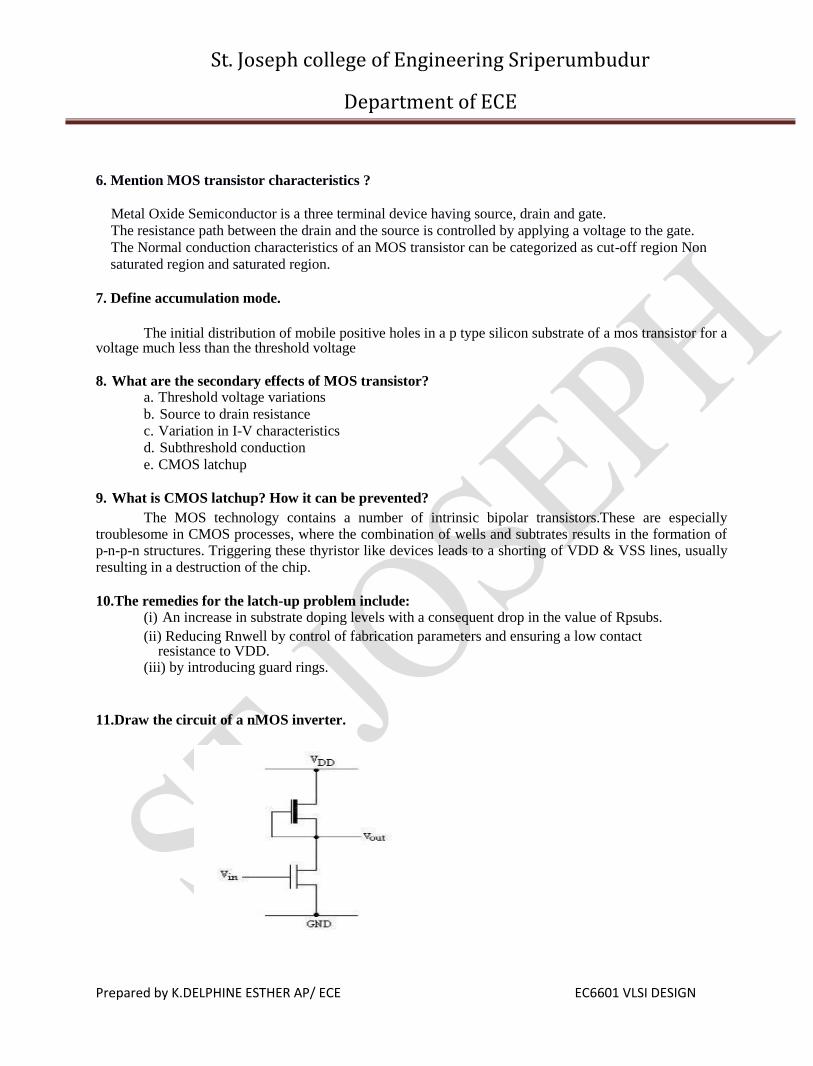
11.Draw the circuit of a nMOS inverter.
St. Joseph college of Engineering Sriperumbudur
Department of ECE
Prepared by K.DELPHINE ESTHER AP/ ECE EC6601 VLSI DESIGN
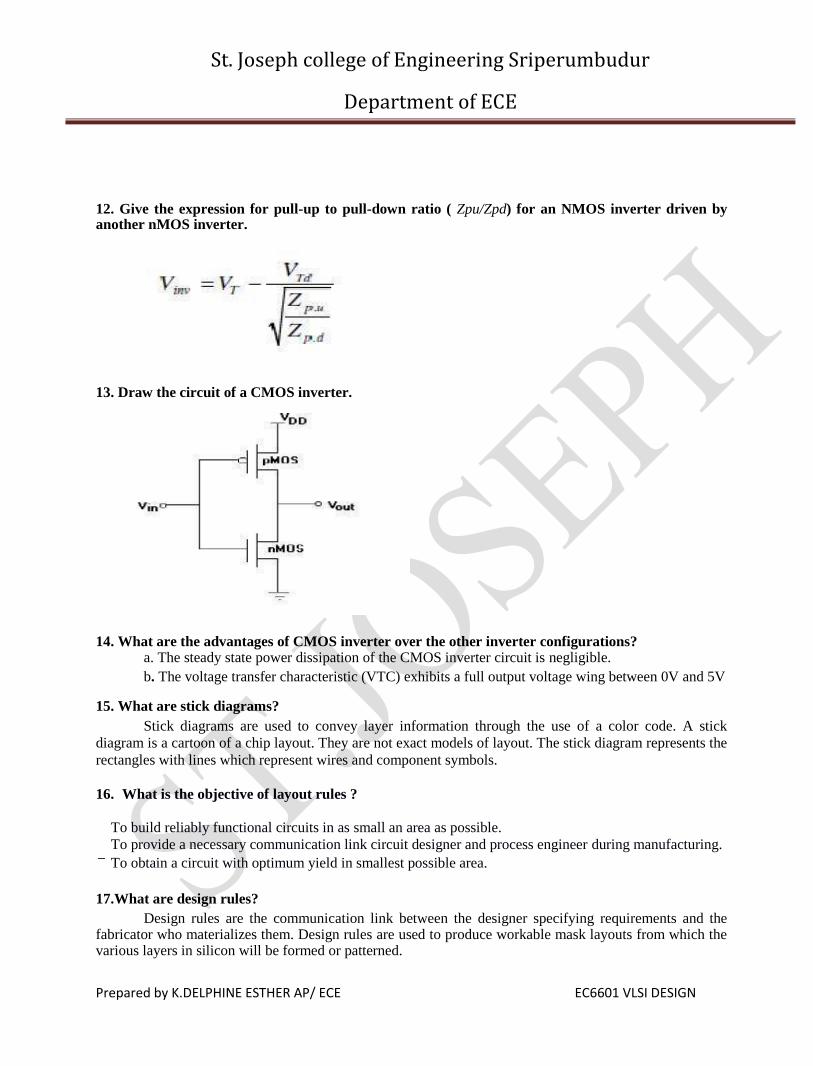
12. Give the expression for pull-up to pull-down ratio ( Zpu/Zpd) for an NMOS inverter driven by another nMOS inverter.
13. Draw the circuit of a CMOS inverter.
14. What are the advantages of CMOS inverter over the other inverter configurations?
a. The steady state power dissipation of the CMOS inverter circuit is negligible. b. The voltage transfer characteristic (VTC) exhibits a full output voltage wing between 0V and 5V
15. What are stick diagrams?
Stick diagrams are used to convey layer information through the use of a color code. A stick
diagram is a cartoon of a chip layout. They are not exact models of layout. The stick diagram represents the
rectangles with lines which represent wires and component symbols.
16. What is the objective of layout rules ?
To build reliably functional circuits in as small an area as possible.
To provide a necessary communication link circuit designer and process engineer during manufacturing.
To obtain a circuit with optimum yield in smallest possible area.
17.What are design rules? Design rules are the communication link between the designer specifying requirements and the
fabricator who materializes them. Design rules are used to produce workable mask layouts from which the various layers in silicon will be formed or patterned.
St. Joseph college of Engineering Sriperumbudur
Department of ECE
Prepared by K.DELPHINE ESTHER AP/ ECE EC6601 VLSI DESIGN
18.What is Moore’s law?
Moore’s law states that the number of transistor would double every 18 months.
19.What is CMOS technology?
Complementary Metal Oxide Semiconductor (CMOS)in which both n-channel MOS and p-channel
MOS are fabricated in the same IC.
20.What are the advantages of CMOS over NMOS technology ?
In CMOS technology the aluminum gates of the transistor are replaced by poly silicon gate.
The main advantage of CMOS over NMOS is low power consumption. In CMOS technology the device
sizes can be easily scalable than NMOS.
The advantages of CMOS technology
Low power consumption.
High performance. Scalable threshold voltage.
High noise margin.
Low output drive current.
PART –B
1. Discuss in detail with a neat layout, the design rules for a CMOS inverter.
2. Discuss in detail with necessary equation the operation of MOSFET and its current voltage
characteristics.
3. Draw and explain the D.C and transfer characteristics of a CMOS inverter with a necessary
conditions for the different regions of operation.
4. Discuss the principle of constant field scaling and also write its effect on device characteristics.
5. Explain the small signal model of MOS transistors with neat diagram and expression.
Draw the stick diagram and layout of a NMOS inverter.
St. Joseph college of Engineering Sriperumbudur
Department of ECE
Prepared by K.DELPHINE ESTHER AP/ ECE EC6601 VLSI DESIGN
UNIT-II
COMBINATIONAL LOGIC CIRCUIT
1. What are two components of Power dissipation? There are two components that establish the amount of power dissipated in a CMOS circuit.
These are: i) Static dissipation due to leakage current or other current drawn continuously from the power supply. ii) Dynamic dissipation due to
- Switching transient current - Charging and discharging of load capacitances.
2. What are the static properties of complementary CMOS Gates? They exhibit rails-to-rail swing with VOH = VDD and VOL = GND.
The circuits have no static power dissipation, since the circuits are designed such that The pull-down and pull-up networks are mutually exclusive.
The analysis of the DC voltage transfer characteristics and the noise margins is more complicated than for the inverter, as these parameters depend upon the data input patterns applied to the gate.
3.What is meant by ratioed logic? In ratioed logic, a gate consists of an nMOS pull-down network that realizes the logic function and a simple load device, which replace the entire pull-up network. A ratioed logic which uses a grounded pMOS load is referred to as a pseudo-nMOS gate.
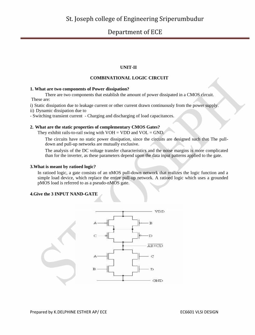
4.Give the 3 INPUT NAND-GATE
St. Joseph college of Engineering Sriperumbudur
Department of ECE
Prepared by K.DELPHINE ESTHER AP/ ECE EC6601 VLSI DESIGN
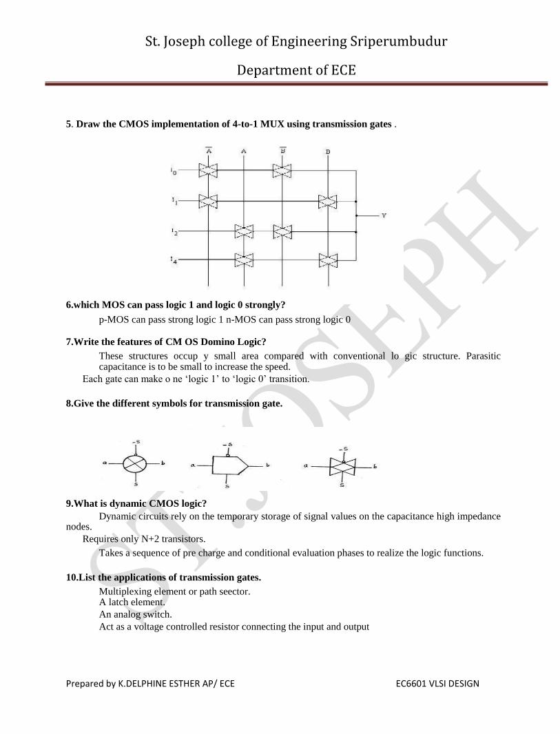
5. Draw the CMOS implementation of 4-to-1 MUX using transmission gates .
6.which MOS can pass logic 1 and logic 0 strongly?
p-MOS can pass strong logic 1 n-MOS can pass strong logic 0 7.Write the features of CM OS Domino Logic?
These structures occup y small area compared with conventional lo gic structure. Parasitic capacitance is to be small to increase the speed.
Each gate can make o ne ‘logic 1’ to ‘logic 0’ transition.
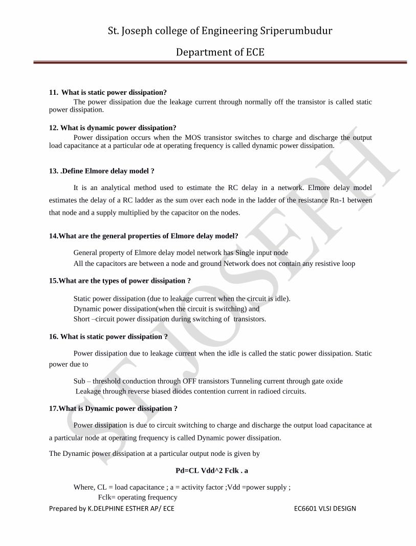
8.Give the different symbols for transmission gate.
9.What is dynamic CMOS logic? Dynamic circuits rely on the temporary storage of signal values on the capacitance high impedance
nodes. Requires only N+2 transistors.
Takes a sequence of pre charge and conditional evaluation phases to realize the logic functions.
10.List the applications of transmission gates.
Multiplexing element or path seector. A latch element. An analog switch. Act as a voltage controlled resistor connecting the input and output
St. Joseph college of Engineering Sriperumbudur
Department of ECE
Prepared by K.DELPHINE ESTHER AP/ ECE EC6601 VLSI DESIGN
11. What is static power dissipation? The power dissipation due the leakage current through normally off the transistor is called static
power dissipation.
12. What is dynamic power dissipation? Power dissipation occurs when the MOS transistor switches to charge and discharge the output
load capacitance at a particular ode at operating frequency is called dynamic power dissipation.
13. .Define Elmore delay model ?
It is an analytical method used to estimate the RC delay in a network. Elmore delay model
estimates the delay of a RC ladder as the sum over each node in the ladder of the resistance Rn-1 between
that node and a supply multiplied by the capacitor on the nodes. 14.What are the general properties of Elmore delay model?
General property of Elmore delay model network has Single input node All the capacitors are between a node and ground Network does not contain any resistive loop
15.What are the types of power dissipation ?
Static power dissipation (due to leakage current when the circuit is idle).
Dynamic power dissipation(when the circuit is switching) and
Short –circuit power dissipation during switching of transistors.
16. What is static power dissipation ?
Power dissipation due to leakage current when the idle is called the static power dissipation. Static
power due to
Sub – threshold conduction through OFF transistors Tunneling current through gate oxide
Leakage through reverse biased diodes contention current in radioed circuits.
17.What is Dynamic power dissipation ?
Power dissipation is due to circuit switching to charge and discharge the output load capacitance at
a particular node at operating frequency is called Dynamic power dissipation. The Dynamic power dissipation at a particular output node is given by
Pd=CL Vdd^2 Fclk . a
Where, CL = load capacitance ; a = activity factor ;Vdd =power supply ; Fclk= operating frequency
St. Joseph college of Engineering Sriperumbudur
Department of ECE
Prepared by K.DELPHINE ESTHER AP/ ECE EC6601 VLSI DESIGN
18.What are the methods to reduce dynamic power dissipation ?
1. Reducing the product of capacitance and its switching frequency .
2. Eliminate logic switching that is not necessary for computation.
3. Reduce activity factor Reduce supply voltage
19.What are the methods to reduce static power dissipation ?
1. By selecting multi threshold voltages on circuit paths with low-Vt transistors while leakage on
other paths with high-Vt transistors.
2. By using two operating modes, active and standby for each function blocks.
3. By adjusting the body bias (i.e) adjusting FBB (Forward Body Bias) in active mode to increase performance and RBB (Reverse Body Bias) in standby mode to reduce leakage.
4. By using sleep transistors to isolate the supply from the block to achieve significant leakage power
savings. 20.What is short circuit power dissipation ?
During switching, both NMOS and PMOS transistors will conduct simultaneously and provide a
direct path between Vdd and the ground rail resulting in short circuit power dissipation
PART – B
1. Discuss in detail about the ratioed circuit and dynamic circuit CMOS logic configurations
2. Describe the basic principle of operation of dynamic CMOS ,domino and NP domino logic with
neat diagrams.
3. Explain the static and dynamic power dissipation in CMOS circuits with necessary diagrams and
expressions.
4. Discuss the design techniques to reduce switching activity in a static and dynamic CMOS circuits.
5. Briefly discuss about the classification of circuit families and comparison of circuit families.
St. Joseph college of Engineering Sriperumbudur
Department of ECE
Prepared by K.DELPHINE ESTHER AP/ ECE EC6601 VLSI DESIGN
UNIT-III
SEQUENTIAL LOGIC CIRCUITS
1. Give the classifications of timing control?
Methods of timing control:
Delay-based timing control
Event-based timing control Level-sensitive timing control
Types of delay based timing control
Regular delay control
Intra-assignment delay control Zero delay control
Types of event-based timing control
Regular event control
Named event control
Event OR control
Level-sensitive timing control
2.What is true single phase clocked register? The True single-phase clocked register (TSPCR) uses a single clock, CLK. For the positive latch,
when CLK is high, the latch is in the transparent mode and corresponds to two cascaded inverters; the latch is non-inverting, and propagates the input to the output. On the other hand, when
CLK=0, both inverters are disabled, and the latch is in the hold mode.
3.what is static CMOS design? In static CMOS,the output is tied to VDD or gnd via a low resistance path and this leads to circuit
implementation robust with good noise immunity.
4.List the important properties of static CMOS design?
Contains a pull up network and pull down network. PDN networks consist of nMOS transistor PUP networks consist of pMOS transistor Each network is the dual of the other network.
5.List the advantages of static CMOS design.
Robust in construction. Good noise immunity Low power consumption.
6.List the limitation of static CMOS design. Increased gate capacitance due to the presence of both pMOS and nMOS transistors.
Output dependence on the previous cycle inputs due to the charges that may be present at internal
inputs. Multiple switching of the output within a cycle depending on the input switching pattern.
St. Joseph college of Engineering Sriperumbudur
Department of ECE
Prepared by K.DELPHINE ESTHER AP/ ECE EC6601 VLSI DESIGN
7.What is dynamic CMOS design? A dynamic logic gate uses clocking and charge storage properties of MOSFETs to implement logic
operations. The clock provides a synchronized data flow in the circuit. 8.what are the properties of dynamic logic design?
Logic function is implemented by the puldown network only. Full swing outputs (VOL=GND and VOH=VDD) Faster switching speeds.
9.What are the limitations of dynamic circuit?
Monotonicitty Leakage Charge sharing Very sensitive to noise.
10.Differnce between synchronous and asynchronous design?
Synchronous Sequential Circuit: Output changes at discrete interval of time. It is a circuit based on an equal state time or a state time defined by external means such as clock. Examples of synchronous sequential circuit are Flip Flops, Synchronous Counter.
Asynchronous Sequential Circuit: Output can be changed at any instant of time by changing the input. It is a circuit whose state time depends solely upon the internal logic circuit delays. Example of asynchronous sequential circuit is Asynchronous Counter.
11.Define latches. A logic circuit that transfers the input states to the output states when signalled, the output there after remaining insensitive to changes in input status until signalled again
12.what are all the difference between latches and registers. Latches are level sensitive i.e they are transparent for certain level .Positive latches let the input
propagate to the output as long as the clock(or enable) is high and hold their previous state when clock(or enable) is low (and vice versa for negative latches) .
Registers on the other hand are edge triggered i.e they transfer input to the output at clock's edges .You
can have a register of a master-slave topology by placing a negative latch after a positive latch (that's what
is usually done for static CMOS registers at digital ICs) .
13.What is the characteristics of Static CMOS design ?
A static CMOS circuit is a combination of two networks – the pull-up network (PUN) and the pull-
down network (PDN) in which at every point in time, each gate output is connected to either VDD or VSS
via a low resistance line. 14.List the important properties of Static CMOS design ?
At any instant of time, the output of the gate is directly connected to VDD and VSS. The function
of the PUN is provide a connection between the output and VDD.
The function of the PDN is provide a connection between the output and VSS .
St. Joseph college of Engineering Sriperumbudur
Department of ECE
Prepared by K.DELPHINE ESTHER AP/ ECE EC6601 VLSI DESIGN
Both PDN and PUN are constructed in mutually exclusive way such that one and only one of the
networks is conducting in steady state. That is, the output node is always a low-impedance node in
steady state. 15.What is Dynamic CMOS logic ?
Dynamic circuits rely on the temporary storage of signal values on the capacitance of high
impedance node.
Requires only N+2 transistors.
Takes a sequence of pre charge and conditional evaluation phases to realizes logic functions.
16.What are the properties of Dynamic logic ?
Logic function is implemented by pull-down network only.
Full swing outputs (VOL= GND and VOH = VDD).
Non-ratioed. Faster switching speeds. Needs a pre charge clock.
17.What are the disadvantages of dynamic CMOS technology ?
A fundamental difficulty with dynamic circuits is a loss of noise immunity and a serious timing
restriction on the inputs of the gate.
Violate monotonicity during evaluation phase.
18.What is CMOS Domino logic ?
A static CMOS inverter placed between dynamic gates which eliminate the monotonicity problem
in dynamic circuits are called CMOS Domino logic. 19.What is called static and dynamic sequencing element ?
A sequencing element with static storage employs some sort of feedback to retain its output value
indefinitely.
A sequencing element with dynamic storage generally maintain its value as charge on a capacitor
that will leak away if not refreshed for a long period of time. 20.What is clock skew ?
In reality clocks have some uncertainty in their arrival times that can cut into the time available for
useful computation is called clock skew.
St. Joseph college of Engineering Sriperumbudur
Department of ECE
Prepared by K.DELPHINE ESTHER AP/ ECE EC6601 VLSI DESIGN
PART – B
1. Write a brief note on sequencing dynamic circuits.
2. Explain in detail about the principle concepts used in sequential circuits.
3. How do you achieve low power in memory circuits? Explain in detail.
4. Discuss in detail about dynamic RAM.
5. Illustrate the principles of synchronizer and arbiter.
St. Joseph college of Engineering Sriperumbudur
Department of ECE
Prepared by K.DELPHINE ESTHER AP/ ECE EC6601 VLSI DESIGN
UNIT-IV
DESIGNING ARITHMETIC BLOCKS
1.What are the advantages of data path operators? To implement the logic function using n-identical circuits.
Data may be arranged to flow in one direction, while any control signals are introduced in an orthogonal direction to the data flow.
2.Define ripple carry adder.
When multiple full adders are used with the carry ins and carry outs chained together then this is called a ripple carry adder.
3.what are the different types of high speed adder?
Carry skip addition. Carry select adder Carry save adder
4.What are the different types if multipliers available?
Array multiplier Booth multiplier Wallace tree multiplier
5.Define booth encoding.
Pipelining reduces cycle time but doesn’t reduce the total time required for multiplication, to speed up
the multiplying process booth encoding is used. Booth’s algorithm takes advantage of the fact that an
adder-subtractor is nearly as fast and small as a simple adder.
6.What is meant by Wallace tree multiplier? Optimized column adder tree Combines all partial products into 2 vectors
Carry and sum outputs combined using a conventional adder Delay is log(n) Irregular routing.
7. What is array multiplier? Each product terms are the implemented using an array structure of AND and OR gate hence it
is called array multiplier.
8.What is meant by barrel shifter? A barrel shifter is a digital circuit that can shift a data word by a specified number of bits in one clock
cycle. It can be implemented as a sequence of multiplexers (mux.), and in such an implementation the
output of one mux is connected to the input of the next mux in a way that depends on the shift distance. 9.Define accumulator
An accumulator is a register in which intermediate arithmetic and logic results are stored. Without a register like an accumulator, it would be necessary to write the result of each calculation (addition, multiplication, shift, etc.) To main memory, perhaps only to be read right back again for use in the next operation.
St. Joseph college of Engineering Sriperumbudur
Department of ECE
Prepared by K.DELPHINE ESTHER AP/ ECE EC6601 VLSI DESIGN
10.How path can be implemented in VLSI system?
A data path is best implemented in a bit –sliced fashion. A single layout is used respectively for
every bit in the data word. This regular approach eases the design effort and results in fast and dense
layouts.
11.Comment on performance of ripple carry adder.
A ripple carry adder has a performance that is linearly proportional to the number of bits. Circuit
optimizations concentrate on reducing the delay of the carry path. A number of circuit topologies exist
providing that careful optimization of the circuit topology and the transistor sizes helps to reduce the
capacitance on the carry bit. 12.What is the logic of adder for increasing its performance ?
Other adder structures use logic optimizations to increase the performance (carry bypass, carry
select, carry look ahead). Performance increase comes at the cost area. 13.What is multiplier circuit ?
A multiplier is nothing more than a collection of cascaded adders. Critical path is far more
complex and optimizations are different compared to adders. 14.Which factors dominate the performance of programmable shifter ?
The performance and the area of a programmable shifter are dominated by the wiring.
15.What is meant by data path ?
A data path is a functional units, such as arithmetic logic units or multipliers, that perform data
processing operations, registers and buses. Along with the control unit it composes the central processing
unit. 16.Write down the expression for worst-case delay for RCA.
t = (n-1)tc+ts
17.Write down the expression to obtain delay for N-bit carry bypass adder.
tadder = tsetup +Mtcarry +(N/M-1)tbypass +(M-1)tcarry + tsum
18.Define Braun multiplier.
The simplest multiplier is the Braun multiplier. All the partial products are computed in parallel,
and then collected through a cascade of Carry Save Adders. The completion time is limited by the depth of
the carry save array, and by the carry propagation in the adder. This multiplier is suitable for positive
operands.
St. Joseph college of Engineering Sriperumbudur
Department of ECE
Prepared by K.DELPHINE ESTHER AP/ ECE EC6601 VLSI DESIGN
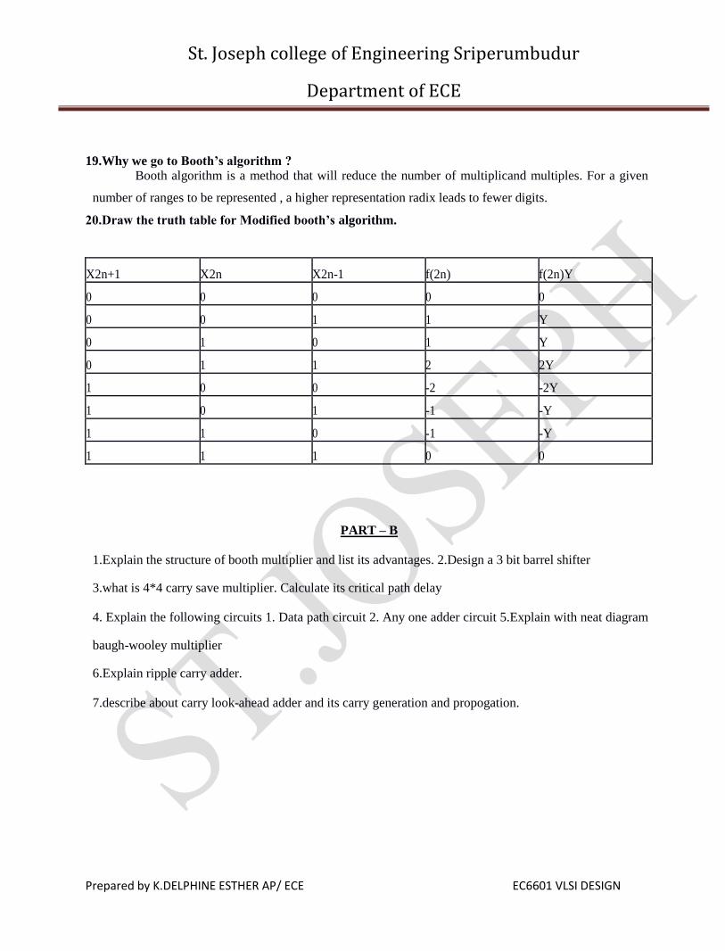
19.Why we go to Booth’s algorithm ?
Booth algorithm is a method that will reduce the number of multiplicand multiples. For a given
number of ranges to be represented , a higher representation radix leads to fewer digits.
20.Draw the truth table for Modified booth’s algorithm.
X2n+1 X2n X2n-1 f(2n) f(2n)Y
0 0 0 0 0
0 0 1 1 Y
0 1 0 1 Y
0 1 1 2 2Y
1 0 0 -2 -2Y
1 0 1 -1 -Y
1 1 0 -1 -Y
1 1 1 0 0
PART – B
1.Explain the structure of booth multiplier and list its advantages. 2.Design a 3 bit barrel shifter
3.what is 4*4 carry save multiplier. Calculate its critical path delay
4. Explain the following circuits 1. Data path circuit 2. Any one adder circuit 5.Explain with neat diagram
baugh-wooley multiplier
6.Explain ripple carry adder.
7.describe about carry look-ahead adder and its carry generation and propogation.
St. Joseph college of Engineering Sriperumbudur
Department of ECE
Prepared by K.DELPHINE ESTHER AP/ ECE EC6601 VLSI DESIGN
UNIT-V
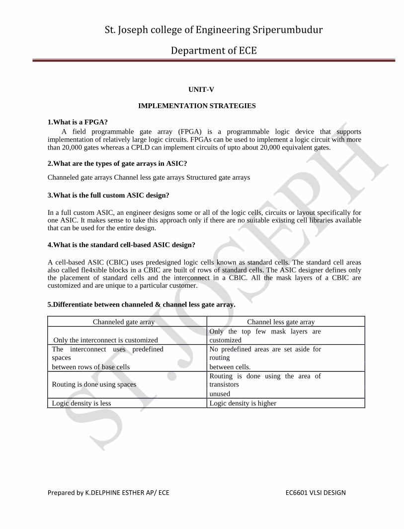
IMPLEMENTATION STRATEGIES 1.What is a FPGA?
A field programmable gate array (FPGA) is a programmable logic device that supports implementation of relatively large logic circuits. FPGAs can be used to implement a logic circuit with more than 20,000 gates whereas a CPLD can implement circuits of upto about 20,000 equivalent gates.
2.What are the types of gate arrays in ASIC? Channeled gate arrays Channel less gate arrays Structured gate arrays
3.What is the full custom ASIC design?
In a full custom ASIC, an engineer designs some or all of the logic cells, circuits or layout specifically for one ASIC. It makes sense to take this approach only if there are no suitable existing cell libraries available that can be used for the entire design.
4.What is the standard cell-based ASIC design?
A cell-based ASIC (CBIC) uses predesigned logic cells known as standard cells. The standard cell areas also called fle4xible blocks in a CBIC are built of rows of standard cells. The ASIC designer defines only the placement of standard cells and the interconnect in a CBIC. All the mask layers of a CBIC are customized and are unique to a particular customer.
5.Differentiate between channeled & channel less gate array.
Channeled gate array Channel less gate array
Only the interconnect is customized
Only the top few mask layers are
customized
The interconnect uses predefined
spaces
No predefined areas are set aside for
routing
between rows of base cells between cells.
Routing is done using spaces
Routing is done using the area of
transistors
unused
Logic density is less Logic density is higher
St. Joseph college of Engineering Sriperumbudur
Department of ECE
Prepared by K.DELPHINE ESTHER AP/ ECE EC6601 VLSI DESIGN
6.Give the constituent of I/O cell in 22V10. 2V10
I/O cell consists of a register
an output 4:1 mux a tristate buffer
a 2:1 input mux It has the following characteristics:
* 12 inputs * 10 I/Os
* product time 9 10 12 14 16 14 12 10 8 * 24 pins
7.Give the different types of ASIC.
Full custom ASICs Semi-custom ASICs o standard cell based ASICs o gate-array based ASICs Programmable ASICs o Programmable Logic Device (PLD)
Field Programmable Gate Array (FPGA).
8.How path can be implemented in VLSI system?
A data path is best implemented in a bit –sliced fashion. A single layout is used respectively for every bit
in the data word. This regular approach eases the design effort and results in fast and dense layouts.
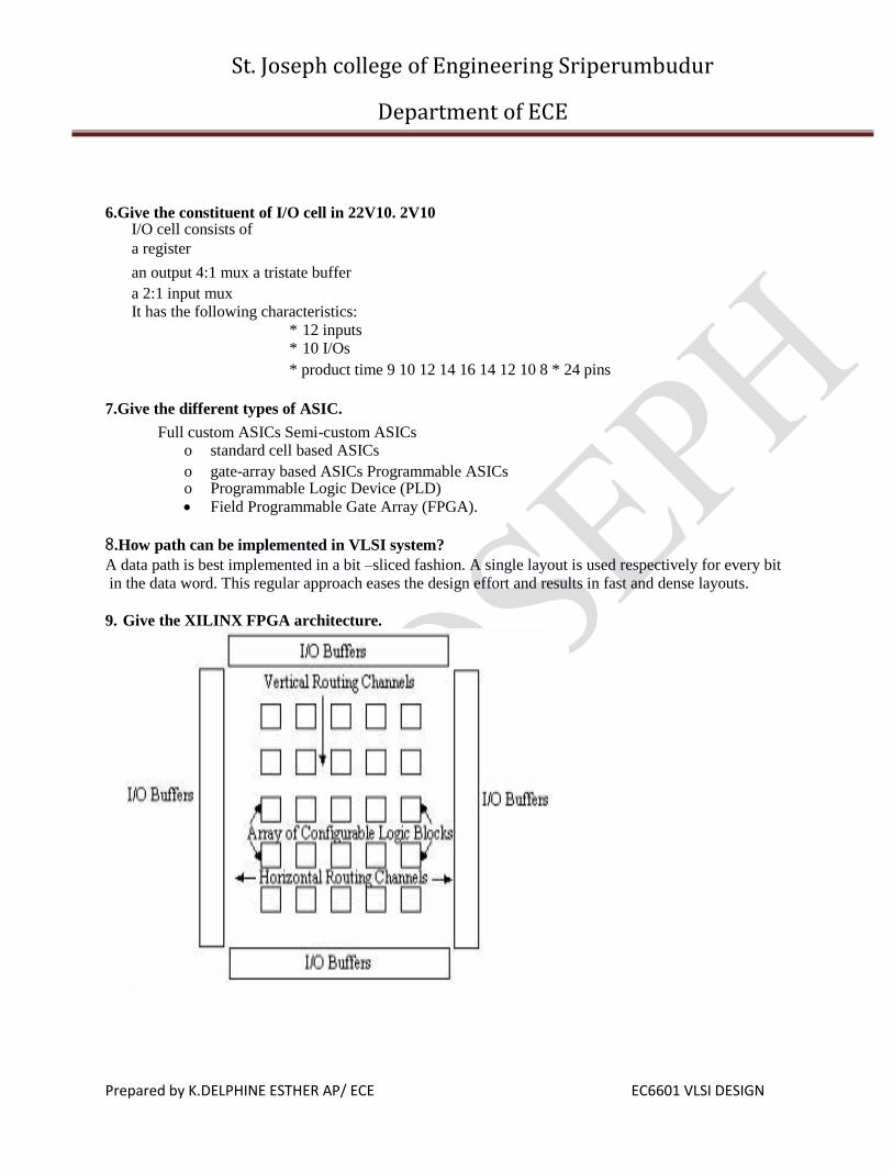
9. Give the XILINX FPGA architecture.
St. Joseph college of Engineering Sriperumbudur
Department of ECE
Prepared by K.DELPHINE ESTHER AP/ ECE EC6601 VLSI DESIGN
10.Give the steps inASIC design flow. o Design entry
o Logic synthesis System partitioning o Prelayout simulation.
o Floorplanning
o Placement o Routing o Extraction
11.What are the different levels of design abstraction at physical design.
Architectural or functional unit Register Transfer-level (RTL)
Logic level Circuit level
12.What are macros.
The logic cells in a gate-array are often called macros.
13.What are programmable Interconnects ?
In a PAL, the device is programmed by changing the characteristics if the switching element. An
alternative would be to program the routing.
14.What are the types of ASICs ?
Types of ASICs are
Full custom ASICs
Semi custom ASICs
15.What are the types of programmable devices ?
Types of programmable devices are
Programmable logic structure
Programmable Interconnect
Reprogrammable Gate Array
16.What are the features of standard celled ASICs ?
All mask layers are customized-transistors and interconnect.
Custom blocks can be embedded
Manufacturing lead time is about eight weeks.
St. Joseph college of Engineering Sriperumbudur
Department of ECE
Prepared by K.DELPHINE ESTHER AP/ ECE EC6601 VLSI DESIGN
17.What are the characteristics of FPGA ?
None of the mask layers are customized A method of programming the basic logic cells and the interconnect. The core is a array of programmable basic logic cells that can implement combinational as well as
sequential logic (flip-flops).
A matrix of programmable interconnect surrounds the basic logic cells. Design turn around is a few
hours.
18.What is programmable logic array ?
A programmable logic array (PLA) is a programmable device used to implement combinational
logic circuits. The PLA has a set of programmable AND planes, which link to a programmable OR planes,
which can then be conditionally complemented to produce an output. This layout allows for a large number
of logic functions to be synthesized in the sum of products (sometimes product of sums) canonical forms. 19.What is meant by programmable logic plane ?
The programmable logic plane is programmable read only memory (PROM) array that allows the
signals present on the devices pins to be routed to an output logic macro cell. 20.Give the application of PLA and the different types of ASIC.
Design and testing of digital circuits.
The different types of ASIC.
1. Full custom ASICs
2. Semicustom ASICs
Standard cell based ASICs
Gate-array based ASICs
3. Programmable ASICs
Programmable Logic Device (PLD) Field Programmable Gate Array (FPGA).
St. Joseph college of Engineering Sriperumbudur
Department of ECE
Prepared by K.DELPHINE ESTHER AP/ ECE EC6601 VLSI DESIGN
PART – B
1.Explain the general architecture of FPGA and bring about different programmable blocks used.
2.Discuss in detail about full custom design and semi custom design.
3.describe about Gate-Array Based ASICs.
4.write short note on programmable Logic Devices.
5.Write short notes on standard cell design and cell libraries.
6.Write the significance of PLA/FSM in VLSI design.
7.Explain the programmable interconnects and I/O blocks used in FPGA.